design methodology for high voltage insulators including ... · pdf fileinsulators including...
TRANSCRIPT

ANSYS, Inc. Proprietary© 2006 ANSYS, Inc.
Design Methodology for High Voltage Insulators Including Effects of Surface Charging
Design Methodology for High Voltage Insulators Including Effects of Surface ChargingRobert TresederEngineering Manager
James BoyeSenior Engineer
Varian Medical SystemsX-ray Products
ANSYS, Inc. Proprietary© 2006 ANSYS, Inc.
History of X-ray Generation
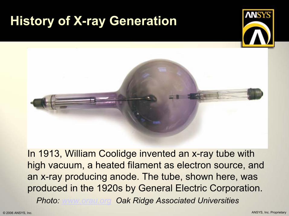
In 1913, William Coolidge invented an x-ray tube with high vacuum, a heated filament as electron source, and an x-ray producing anode. The tube, shown here, was produced in the 1920s by General Electric Corporation.
Photo: www.orau.org Oak Ridge Associated Universities

ANSYS, Inc. Proprietary© 2006 ANSYS, Inc.
History of X-ray Generation
Early x-ray equipment posed risk of high voltage shock and unregulated x-ray dose.
ANSYS, Inc. Proprietary© 2006 ANSYS, Inc.
History of X-ray Generation
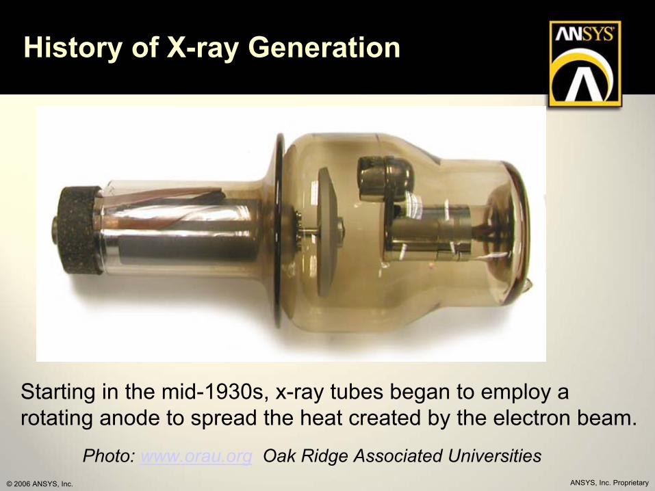
Photo: www.orau.org Oak Ridge Associated Universities
Starting in the mid-1930s, x-ray tubes began to employ a rotating anode to spread the heat created by the electron beam.

ANSYS, Inc. Proprietary© 2006 ANSYS, Inc.
History of X-ray Generation
Shown here are typical metal-centered tubes for mammography and medical CT.
In the 1980s Varian pioneered the metal-centered x-ray tube. Replacing the glass bulb with a metal frame results in a tube able to withstand the stresses of modern medical equipment.

ANSYS, Inc. Proprietary© 2006 ANSYS, Inc.
History of X-ray Generation
Modern CT gantries spin at 2~3 revolutions/second. The imaging system rotates around the patient providing several thousand views per revolution for 3-D image reconstruction. Each view uses grayscale data from as many as 50,000 x-ray detectors.
ANSYS, Inc. Proprietary© 2006 ANSYS, Inc.
History of X-ray Generation
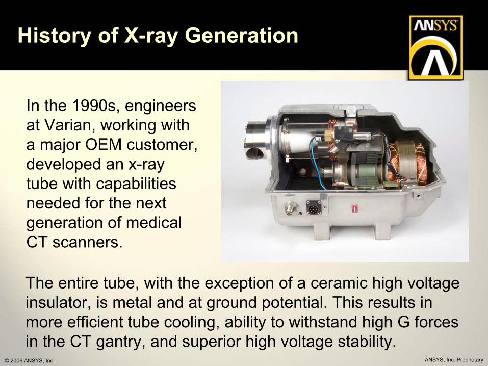
In the 1990s, engineers at Varian, working with a major OEM customer, developed an x-ray tube with capabilities needed for the next generation of medical CT scanners.
The entire tube, with the exception of a ceramic high voltage insulator, is metal and at ground potential. This results in more efficient tube cooling, ability to withstand high G forces in the CT gantry, and superior high voltage stability.

ANSYS, Inc. Proprietary© 2006 ANSYS, Inc.
X-ray Tube High Voltage Insulator
Insulator roles:
•High voltage stand-off
•Vacuum wall
•Structural support
•Heat conduction
ANSYS, Inc. Proprietary© 2006 ANSYS, Inc.
The Old Way to Design
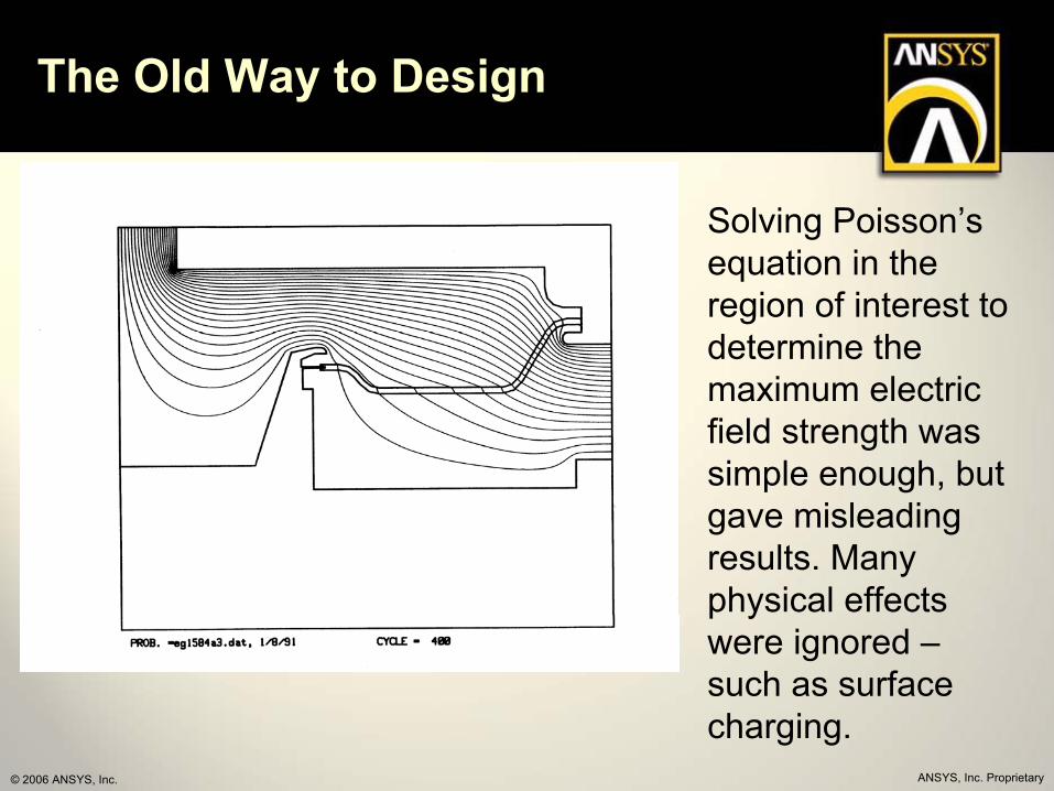
Solving Poisson’s equation in the region of interest to determine the maximum electric field strength was simple enough, but gave misleading results. Many physical effects were ignored –such as surface charging.
ANSYS, Inc. Proprietary© 2006 ANSYS, Inc.
The OBC (Oblique Boundary Condition) Method
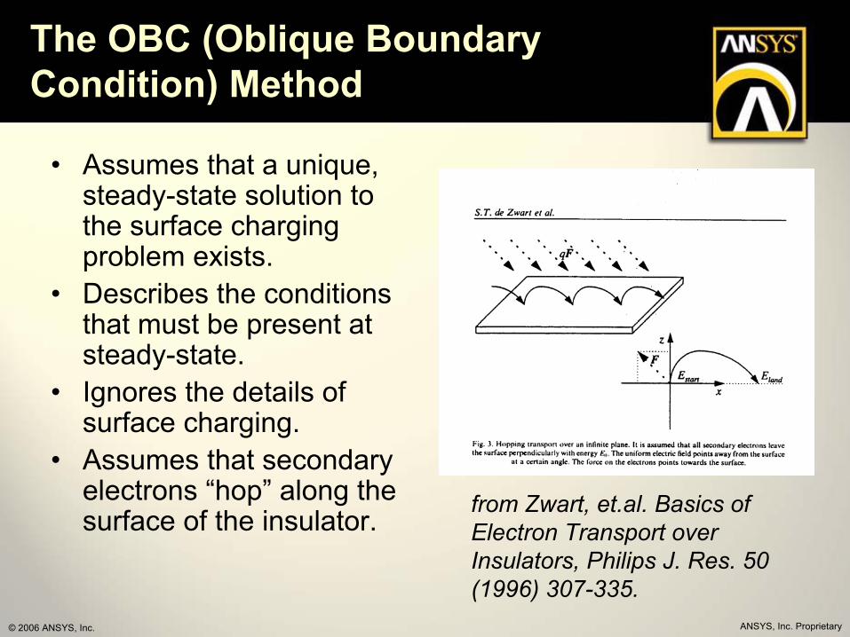
• Assumes that a unique, steady-state solution to the surface charging problem exists.
• Describes the conditions that must be present at steady-state.
• Ignores the details of surface charging.
• Assumes that secondary electrons “hop” along the surface of the insulator. from Zwart, et.al. Basics of
Electron Transport over Insulators, Philips J. Res. 50 (1996) 307-335.

ANSYS, Inc. Proprietary© 2006 ANSYS, Inc.
The OBC (Oblique Boundary Condition) Method
• Ratio of the perpendicular to normal electric field depends on material properties only.
from Zwart, et.al. Basics of Electron Transport over Insulators, Philips J. Res. 50 (1996) 307-335.

ANSYS, Inc. Proprietary© 2006 ANSYS, Inc.
The OBC (Oblique Boundary Condition) Method
3
1 (4)4
v S
dv r dSr r r
ϕϕ ρ ϕπε
′ ′ ′∇ ′ ′= + − ⋅ ∫ ∫rr rGeneral potential solution with surface
BCs and volume charges:
Divide the charge surface into a finite number of small areas: 1
(5)N
n nn
ρ α ρ=
=∑
Each small area (n=1 to N) will contribute to the potential solution:
1 (6)4
nn n
Sv
dv dSr r
ϕϕ ρπε
′ ′′ ∇ = + ⋅ ∫ ∫r
r
The n=0 load case is subject to BCspresent with no charges absent:
00 0 3 (7)
S
r dSr r
ϕϕ ϕ ′′∇′= − ⋅ ∫
rr r
ANSYS, Inc. Proprietary© 2006 ANSYS, Inc.
The OBC (Oblique Boundary Condition) Method
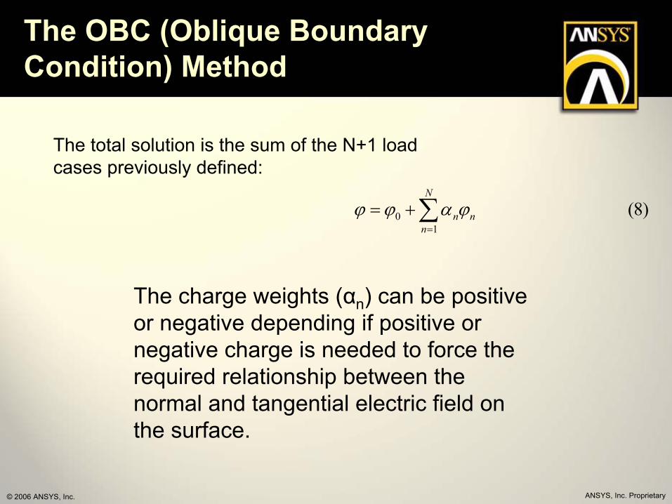
The total solution is the sum of the N+1 load cases previously defined:
01
(8)N
n nn
ϕ ϕ α ϕ=
= +∑
The charge weights (αn) can be positive or negative depending if positive or negative charge is needed to force the required relationship between the normal and tangential electric field on the surface.

ANSYS, Inc. Proprietary© 2006 ANSYS, Inc.
The OBC (Oblique Boundary Condition) Method
( )1
0 0 (13)F F F Fρ ρα µ µ−⊥ ⊥ = − − ⋅ −
For each load case, ANSYS calculates the electric fields, APDL commands write the F vectors to a text file. An external program calculates the charge weights. This program outputs the weights in the form of ANSYS SFE commands on element edges.
The OBC solution is a load superposition of the N+1 cases:
0
0
(14 )
(14 )
F F F a
F F F bρ
ρ
α
α
⊥ ⊥ ⊥= + ⋅
= + ⋅

ANSYS, Inc. Proprietary© 2006 ANSYS, Inc.
Enloe Diode Test Case
2-D plane parallel cathode and anode surfaces with the vacuum gap partially filled with a dielectric insulator.
C.L. Enloe, “The equilibrium charge distribution and electric field at a vacuum/dielectric interface” J. Appl. Phys. Vol 65, No 9, pp3329-3334, 1989.

ANSYS, Inc. Proprietary© 2006 ANSYS, Inc.
Enloe Diode Test Case
Good agreement with Enloe with regards to the computed potential along the dielectric surface without charging…

ANSYS, Inc. Proprietary© 2006 ANSYS, Inc.
Enloe Diode Test Case
… and with surface charging.

ANSYS, Inc. Proprietary© 2006 ANSYS, Inc.
Brainard and Jensen ‘Neutron Tube’Test Case
J.P. Brainard and D. Jensen, “Electron avalanche and surface charging on alumina insulators during pulsed high-voltage stress” J. Appl. Phys. Vol 45, No 8, pp3260-3265, 1974.
Electric fields in a neutron tube with ceramic insulator subject to surface charging.

ANSYS, Inc. Proprietary© 2006 ANSYS, Inc.
Brainard and Jensen ‘Neutron Tube’Test Case
Comparison of results:
charged
uncharged

ANSYS, Inc. Proprietary© 2006 ANSYS, Inc.
Brainard and Jensen ‘Neutron Tube’Test Case
Comparison of results: charge density
ANSYS, Inc. Proprietary© 2006 ANSYS, Inc.
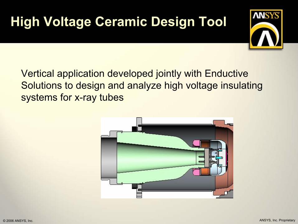
High Voltage Ceramic Design Tool
Vertical application developed jointly with EnductiveSolutions to design and analyze high voltage insulating systems for x-ray tubes

ANSYS, Inc. Proprietary© 2006 ANSYS, Inc.
High Voltage Ceramic Design Tool
•Create model within the SolidWorksenvironment
ANSYS, Inc. Proprietary© 2006 ANSYS, Inc.
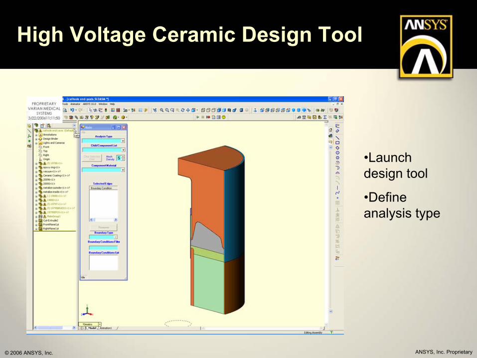
High Voltage Ceramic Design Tool
•Launch design tool
•Define analysis type
ANSYS, Inc. Proprietary© 2006 ANSYS, Inc.
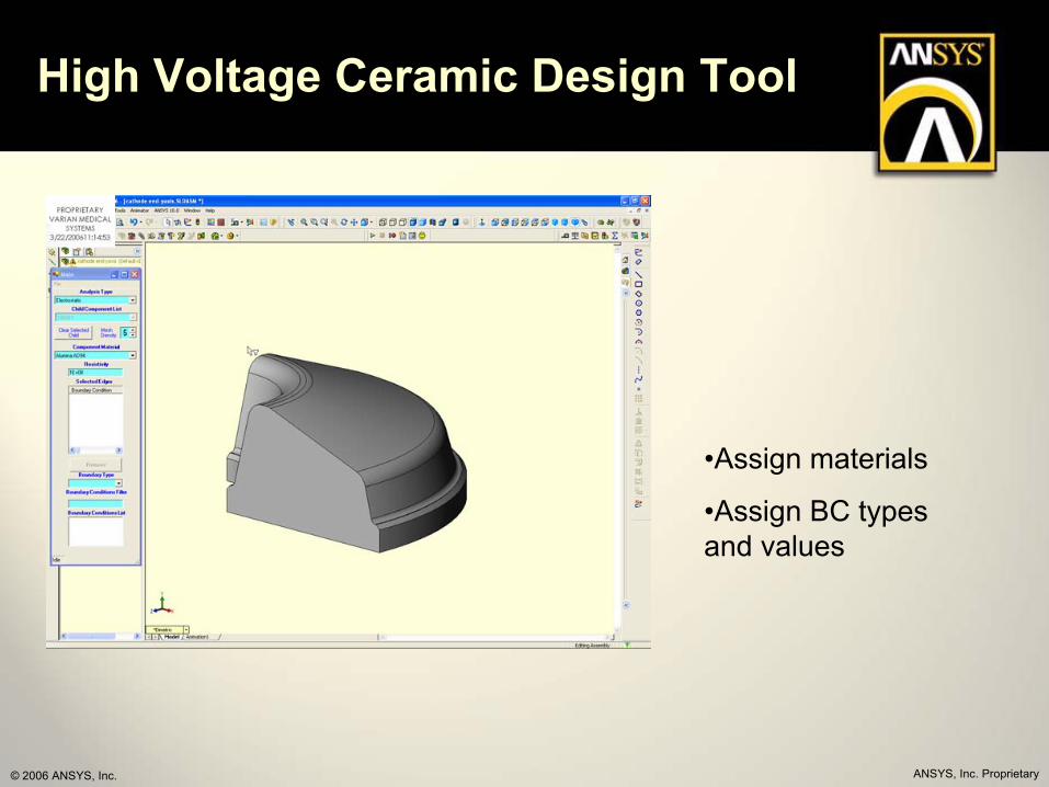
High Voltage Ceramic Design Tool
•Assign materials
•Assign BC types and values

ANSYS, Inc. Proprietary© 2006 ANSYS, Inc.
High Voltage Ceramic Design Tool
Create files for ANSYS:
•Materials file
•SolidWorksassembly file
•ANSYS input command file
•IGES solid model file
Launch ANSYS

ANSYS, Inc. Proprietary© 2006 ANSYS, Inc.
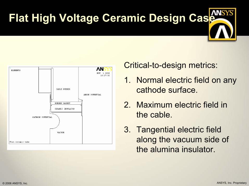
Flat High Voltage Ceramic Design Case
•Axisymmetric geometry
•Inner electrode at cathode (negative) potential
•Outer electrode at ground potential
•Electrostatic solution, with and without surface charging
•Electrical conduction solution
ANSYS, Inc. Proprietary© 2006 ANSYS, Inc.
Flat High Voltage Ceramic Design Case
Critical-to-design metrics:
1. Normal electric field on any cathode surface.
2. Maximum electric field in the cable.
3. Tangential electric field along the vacuum side of the alumina insulator.

ANSYS, Inc. Proprietary© 2006 ANSYS, Inc.
Flat High Voltage Ceramic Design Case
Electrostatic solution equipotentials, with and without charging

ANSYS, Inc. Proprietary© 2006 ANSYS, Inc.
Flat High Voltage Ceramic Design Case
Conduction solution equipotentials

ANSYS, Inc. Proprietary© 2006 ANSYS, Inc.
Flat High Voltage Ceramic Design Case
Charge distribution along the vacuum side of the alumina insulator
ANSYS, Inc. Proprietary© 2006 ANSYS, Inc.
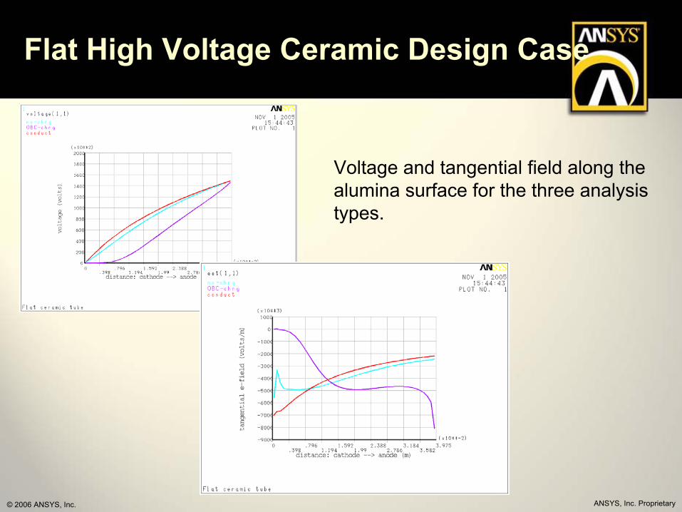
Flat High Voltage Ceramic Design Case
Voltage and tangential field along the alumina surface for the three analysis types.
ANSYS, Inc. Proprietary© 2006 ANSYS, Inc.
Conclusions
• Presence of surface charge on the vacuum side of the insulator will significantly alter the critical-to-design electric field metrics.
• OBC method for estimating the surface charge is in good agreement with published test cases.
• The vertical application developed jointly by Varian Medical Systems and EnductiveSolutions using the OBC method and the ANSYS solver is an easy-to-use, practical design tool.

ANSYS, Inc. Proprietary© 2006 ANSYS, Inc.
Thank You
www.varian.com/xray