design of low power level-converting retention flip … · design of low power level-converting...
TRANSCRIPT

International Conference on Emerging Engineering Trends and Science (ICEETS – 2016)
ISSN : 2348 – 8549 http://www.internationaljournalssrg.org Page 44
Design of Low Power Level-Converting Retention Flip-Flop using LSSR technique for Zigbee SoCs
Muthu Lakshmi R1, Muthuviji K2, Sridevi N3 (student)
Karpagadevi T4 (Asst.professor)
Dept of ECE, P.S.R.Rengasamy College of Engineering for Women, Sivakasi.
Abstract:
In this paper, we propose the design of low power level-converting retention flip-flop
(RFF)using LSSR technique for Zigbee System-on-chips (SoCs).The proposed retention flip-flop allows
the voltage regulator which generates the core
supply voltage (VDD, core) is turned off during the standby mode and thus reduces the standby power
and dc current of the Zigbee SoCs. This method is
the combination of the feature of both, LECTOR approach and the forced stack technique. In
LECTOR approach, the gate terminal is controlled by the source of the other. In forced stack
technique, Transistors in PULL UP and PULL
DOWN networks are replaced as two half sized transistors. In the proposed technique, two leakage
control transistors will be added between the PULL
UP and PULL DOWN networks. It will provide the limitation of area to preserve the circuit state during
sleep mode. This technique will provide good
leakage.
Index Terms: retention flip-flop (RFF), standby
mode, sleep mode.
I. INTRODUCTION:
Power consumption has become the major concern of VLSI circuit design over launching of battery
operated applications. In today’s Electronic
industries, Low Power has emerged as basic theme. The need of low power has caused a major shift
where power dissipation has become as important
consideration as performance and area. Static power
and Dynamic power determine the power consumption in CMOS circuit. Static power includes
sub-threshold leakage, junction leakage and gate
Leakage due to tunneling. Dynamic power includes charging and discharging power and short circuit
Power. VLSI fabrication technology is leading to
smaller feature size and threshold voltages have been scaling down for decades in order to achieve high
performance. Scaling down the feature size and
threshold voltage increases sub-threshold leakage current. This leads to short channel effect which
increases sub-threshold leakage current exponentially. This ultimately increases the leakage
power. There are several VLSI techniques for
reducing the leakage power. These techniques provide an efficient way to reduce leakage power but
the major drawback is that they limit their
applications. In this paper, we propose Lector Stack State Retention technique that reduces not only
leakage power but also dynamic power. We have compared our technique with the previous techniques
existing.
II. REVIEW OF EARLIER LOW LEAKAGE
POWER TECHNIQUES
State Preserving and State Reserving are the two techniques involved in Leakage Power reduction. The
Circuit state is retained in state preserving technique.
The Current output Boolean value of the circuit might be lost in state reserving technique. The most
commonly used approach is the Sleep Approach. In

International Conference on Emerging Engineering Trends and Science (ICEETS – 2016)
ISSN : 2348 – 8549 http://www.internationaljournalssrg.org Page 45
this approach, a sleep PMOS transistor is placed
between Vdd and the pull-up network of a circuit and a sleep NMOS transistor is placed between pull-down
network and Gnd. The sleep transistors turn off the
circuit by cutting of the Power rails. These transistors are turned on when the circuit is active and they are
turned off when the circuit is idle. This technique can reduce leakage power effectively by cutting off the
power source. Another technique for leakage power
reduction is the Stack Approach. It forces a stack effect by breaking down an existing transistor into
two equal half transistors. These half transistors
replace the transistors in pull-up and pull-down networks. The Sleepy stack approach is the
combination of Sleep and Stack approach. It is similar to that of the stack approach. During Sleep
mode, stacked transistors suppress leakage current in
saving state and sleep transistors are turned off. These sleep transistors are placed in parallel to one of
the stacked transistors. This reduces the resistance of
the path so that delay is decreased during the active mode.
Figure 1: Sleepy Stack
Dual stack Approach is compared with well-known previous approaches, i.e., the sleepy stack, dual sleep
and sleep transistor methods. In sleep mode, the sleep
transistors are off, i.e. transistor N5 and P5 are off. We do so by making S=0 and hence S=1. Now we
see that the other 4 transistors P6, P7 and N6, N7 connect the main circuit with power rail. Here we use
2 pmos in the pull-down network and 2 nmos in the
pull up network. The advantage is that nmos degrades
the high logic level while pmos degrades the low logic level. The pass transistors decreases the voltage
applied across the main circuit.
Figure 2: Dual Stack Approach
Power Gating and Multi-Threshold CMOS: The most natural way of lowering the leakage power
dissipation of a VLSI circuit in the STANDBY state
is to turn off its supply voltage. This can be done by using one PMOS transistor and one NMOS transistor
in series with the transistors of each logic block to Create a virtual ground and a virtual power supply.
But in practice only one transistor is necessary.
Because of their lower on-resistance, NMOS transistors are usually used. In the ACTIVE state, the
sleep transistor is on. Therefore, the circuit functions
as usual. In the STANDBY state, the transistor is turned off, which disconnects the gate from the
ground.
III. PROPOSED LOW POWER STATE
RETENTION TECHNIQUE
A novel leakage power reduction technique is proposed in this work i.e. LSSR [LECTOR (Leakage
Control TransistOR (LECTOR)) Stacked State

International Conference on Emerging Engineering Trends and Science (ICEETS – 2016)
ISSN : 2348 – 8549 http://www.internationaljournalssrg.org Page 46
Retention]. The LECTOR method inserts two extra
Leakage Control Transistors (a P-type and an N-type) within the gate, in which the gate terminal of each
Leakage Control Transistor is controlled by the
source of the other. This technique has very good low leak operation but there is no provision of sleep mode
of operation, to overcome this problem extra retention transistors are connected to the output so
that during sleep mode the logic state is maintained.
Hence we combine the advantages of LECTOR method and the Forced Stack Technique to reduce the
overall power dissipation without compromise with
the loss of state (state destructive). So, we call this as a state-preserving technique; where circuit state is
retained.
A. LECTOR Technique:
The LECTOR method inserts two extra Leakage Control Transistors (a P-type and an N-type) within
the gate, in which the gate terminal of each Leakage
Control Transistor is controlled by the source of the other. This is stated based on the observation that a
state is far less leaky with more than one OFF
transistor in a path from supply voltage to ground compared to a state with only one OFF transistor in
the path. The number of OFF transistors is related to leakage power as shown in Figure 3, the arrangement
of LECTOR is shown in Figure 4.
Figure 3: Stack Effect on leakage Current
Figure 4: LECTOR technique
B. Forced Stack Technique:
Another technique to reduce leakage current is
Forced stack technique, in which a transistor is replace by two half size transistors, as shown in
Figure 5, both pmos and nmos. Transistors in PULL
UP and PULL DOWN networks are replaced as two half sized transistors. When the two transistors are
turned off together induced reverse bias between the two transistors results in sub threshold leakage
current reduction. However divided transistors
increase delay significantly.
Figure 5: Forced Stack technique

International Conference on Emerging Engineering Trends and Science (ICEETS – 2016)
ISSN : 2348 – 8549 http://www.internationaljournalssrg.org Page 47
C. Proposed LSSR: In this section we introduce a new leakage current
reduction technique for CMOS circuit design. Figure
7 shows the LECTOR stack technique which is the combination of LECTOR and Forced stack
techniques. As it combines the features of the above mentioned techniques, two gated leakage transistors
are introduced between pull up and pull down
networks with high threshold voltage, then stack effect is added to pull up and pull down networks by
dividing each transistor in to half size transistors (i.e.,
W/2). As more stack effect can be introduced, due to high threshold voltage gated leakage transistors and
half size stacked transistors, ultimately more leakage current reduction can be achieved with the proposed
technique. Though the leakage reduction techniques
discussed in above section 2 could achieve leakage current reduction with the penalty of delay but the
proposed technique can achieve more leakage current
reduction without delay penalty. From Figure 6 we can explain modes of operation of LSSR. The LSSR
logic gate has four modes of operation.
a) Active Mode: Both sleep control signals slp = 0
and slpb = 1 are used to switch on the sleep transistors in leakage control block. Thus the virtual
ground node VG is at ground potential and the virtual
power node VP is at VDD. The gate thus sees good potential difference across nodes VP and VG. The
gate functions as per the truth table with good output
logic levels.
Figure 6: LSSR logic
Figure 7: LSSR stack technique
b) Deep Sleep Mode: The sleep signals are held at slp
= 1 and slpb = 0 states to switch off all the sleep
transistors in both pull up and pull down leakage control blocks. Thus the actual power and ground
path are broken and the circuit experiences lower voltage across the nodes VP and VG. A very high
resistance low leakage current with the output at
good logic 0 level. A path is established between VDD and ground due to the parallel combination of
the off resistance of sleep transistors and the leakage
current flowing through the circuit reduces significantly and hence lowest power dissipation.
c) State Retention Mode 1: The sleep signals are
maintained at slp = 0 and slpb = 0. The circuit sees a
higher than ground voltage at the node VG and full VDD at the node VP. The state retention takes place
with low leakage current with the output at good
logic 1 level.
d) State Retention Mode 0: The sleep control
signals are maintained at slp = 1 and slpb = 1. The connection to actual ground is complete, the node VP
is at lower VDD. Thus the state retention takes place with low leakage current with the output at good
logic 0 level.

International Conference on Emerging Engineering Trends and Science (ICEETS – 2016)
ISSN : 2348 – 8549 http://www.internationaljournalssrg.org Page 48
Figure 8: Level converting retention flip flop using MTCMOS technique
Figure 9: Transient Analysis
Figure 10: Level converting retention flip flop
using Pull-down Network
Figure 11: Transient Analysis
Figure 12: Power and delay analysis using
MTCMOS technique
Figure 13: Power and delay analysis using Pull-down Network
International Conference on Emerging Engineering Trends and Science (ICEETS – 2016)
ISSN : 2348 – 8549 http://www.internationaljournalssrg.org Page 49
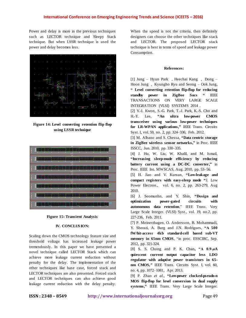
Power and delay is more in the previous techniques
such as LECTOR technique and Sleepy Stack technique. But when LSSR technique is used the
power and delay becomes less.
Figure 14: Level converting retention flip flop
using LSSR technique
Figure 15: Transient Analysis
IV. CONCLUS ION: Scaling down the CMOS technology feature size and
threshold voltage has increased leakage power
tremendously. In this paper we have presented a novel technique called LECTOR Stack which can
achieve more leakage current reduction without penalty for the delay. The implementation of the
other techniques like base case, forced stack and
LECTOR techniques are also presented. Forced stack and LECTOR techniques can also achieve good
leakage current reduction with the delay penalty.
When the speed is not the criteria, then definitely
designers can choose the other techniques like stack and LECTOR. The proposed LECTOR stack
technique is best in terms of speed and leakage power
Consumption.
References:
[1] Jung – Hyun Park , Heechai Kang , Dong – Hoon Jung , Kyungho Ryu and Seong – Ook Jung,
“ Level converting retention flip-flop for reducing
standby power in ZigBee Socs “ IEEE TRANSACTIONS ON VERY LARGE SCALE
INTEGRATION (VLSI) SYSTEMS 2014 . [2] Y.-I. Kwon, S.-G. Park, T.-J. Park, K.-S. Cho and
H.-Y. Lee, “An ultra low-power CMOS
transceiver using various low-power techniques for LR-WPAN applications ,” IEEE Trans. Circuits
Syst. I, vol. 59, no. 2, pp. 324–336, Feb. 2012.
[3] M. Albano and S. Chessa, “Data centric storage in ZigBee wireless sensor networks ,” in Proc. IEEE
ISSCC, Jun. 2010, pp. 330–335.
[4] J. Hu, W. Liu, W. Khalil, and M. Ismail, “Increasing sleep-mode efficiency by reducing
battery current using a DC-DC converter,” in Proc. IEEE Int. MWSCAS, Aug. 2010, pp. 53–56.
[5] H. Jiao and V. Kursun, “Low-leakage and
compact registers with easy-sleep mode “J. Low Power Electron., vol. 6, no. 2, pp. 263-279, Aug
2010.
[6] J. Seomunhn, and Y. Shin, “Design and optimization power-gated circuits with
autonomous data retention,” IEEE Trans. Very
Large Scale Integer. (VLSI) Syst., vol. 19, no.2, pp.
227-236, Feb. 2011.
[7] P. Meinerzhagen, O. Andersson, B. Mohammadi, Y. Sherazi, A. Burg and J.N. Rodrigues, “A 500
fW/bit-access 4kb standard-cell based sub-VT
memory in 65nm CMOS , “in proc. ESSCIRC, Sep. 2012, pp. 321-324. [8] S. S. Chong and P. K. Chan, “A 0.9-μA
quiescent current output capacitor less LDO regulator with adaptive power transistors in 65-nm CMOS,” IEEE Trans. Circuits Syst. I, vol. 60,
no. 4, pp. 1072–1081, Apr. 2013.
[9] P. Zhao et al., “Low-power clocked-pseudo-n
MOS flip-flop for level conversion in dual supply systems,” IEEE Trans. Very Large Scale Integer.

International Conference on Emerging Engineering Trends and Science (ICEETS – 2016)
ISSN : 2348 – 8549 http://www.internationaljournalssrg.org Page 50
(VLSI) Syst., vol. 17, no. 9, pp. 1196–1202, Sep.
2009. [10] Anu Tonk, Shilpa Goyal, and “A Literature
Review on Leakage and Power Reduction
Techniques in CMOS VLSI DESIGN, “International Journal on Recent and Innovation
Trends in Computing and Communication ISSN: 2321-8169 Volume: 3 Issue: 2 554 – 558.