design of pipeline analog to digital converter · design of pipeline analog to digital converter...
TRANSCRIPT

1 | P a g e
Design of Pipeline Analog to Digital Converter
Vivek Tripathi, Chandrajit Debnath, Rakesh Malik
STMicroelectronics
The pipeline analog-to-digital converter (ADC) architecture is the most popular topology for video processing,
telecommunications, digital imaging etc. designs because its speed is comparable to the parallel or flash
architecture, whereas the implementation area and power dissipation are significantly smaller.
Both advantages stem from the concurrent operation of the stages, that is, at any time, the first stage operates on
the most recent sample while all other stages operate on residues from previous samples. Once the pipeline is
primed, converted digital data are always available at every clock cycle.
Also, since the stages operate concurrently, the number of stages used to obtain a given resolution is not
constrained by the required throughput rate. Therefore, under some constraints (such as the total resolution), the
number of stages may be chosen to minimize the required die area.
Like other ADC architectures, the pipeline ADC power consumption increases with required signal bandwidth,
thus making it one of the major contributors to power consumption in a wideband digital video receiver
subsystem. Pipeline ADC’s are used in high Speed(10 MSPS -500 MSPS) data acquisition systems e.g. Low
power mobile, cable front end, medical equipment, WiFi, Set Top Box, WLAN etc. SAR ADCs are used for
Low speed (1MSPS- 10MSPS) data acquisition systems e.g. Automotive, Battery management,
Microcontrollers etc. Sigma-Delta ADCs are used in audio applications. For sensor applications, Industrial
control & DC measurements either SAR or Sigma delta ADCs are used depending upon the accuracy & speed.
For RF applications (GHz data acquisition), Flash ADC is used. This paper will focus on the design technique
& concerns of Pipeline ADC.
Fig. 1 shows a block diagram of a general pipelined ADC with k stages. Each stage contains a sample-and-hold
amplifier (SHA), a low-resolution analog-to-digital sub-converter (ADSC), a low-resolution digital-to-analog
converter (DAC), and a subtractor. To begin a conversion, the input is sampled and held. The held input is then
converted into a digital code by the first-stage low-resolution flash A/D converter and back into an analog
signal by the first-stage low-resolution D/A converter. The difference between the D/A converter output and the
held input is the residue that is amplified and sent to the next stage where this process is repeated. At any
instant, while the first stage processes the current input sample, the second stage processes the amplified residue
of the previous input sample from the first stage. Because sequential stages simultaneously work on residues
from successively sampled inputs, the digital outputs from each stage correspond to input samples at different
times. Digital latches are needed to synchronize the outputs from different stages.
Fig.1: Block diagram of Pipeline ADC
Vin
Stage 1
Stage 2
Stage k
m1
m2
mk
DAC ADADCC
2𝑚 + +
-
Vout
mi bits
Vin
ADC DAC

2 | P a g e
2 BIT/STAGE PIPELINE ARCHITECTURE:
Fig 2: Ideal Transfer Function of a 2-bit Pipelined Stage
The stage gain is 4x to maximize the dynamic range of the subsequent stage, and to allow for reuse of the
reference voltages.
An error in the stage ADC threshold (due to an offset) alters the transfer function as shown in Fig. 3
00 01 10 11
Vout
Vin
+VR
-VR
-3VR/4 -V
R/2 -V
R/4 0 V
R/4 V
R/2 3V
R/4 -V
R
2BIT DAC
Vout X4
+
-
2BIT
ADC
Vin
2 BITS
+

3 | P a g e
Fig. 3: Transfer function with errors in sub-ADC
Thus threshold errors lead to stage outputs that exceed the full-scale input to the subsequent stage. This will
saturate the second stage and cause missing information. To eliminate this problem, one can increase the range
of the second stage sub-ADC or equivalently reduce the inter-stage gain of the first stage to tolerate sub-ADC
error.
When the inter stage gain is reduced to 2, the transfer function becomes as shown in Fig. 4.
00 01 10 11
Vout
Vin
+VR
-VR
-3VR/4 -V
R/2 -V
R/4 0 V
R/4 V
R/2 3V
R/4 -V
R
00 01 10 11
Vout
Vin
+VR
-VR
-3VR/4
-VR/2
-VR/4 0 V
R/4 V
R/2 3V
R/4
+VR/2
-VR/2

4 | P a g e
Fig.4: Transfer Function with Inter stage Gain of 2 and sub-ADC Error
This allows the sub-ADC error to be as large as VR/4 and the output is still in the input range of the following
stage. However, when a sub-ADC error is present without digital correction, the error will appear in the final
digital output. Now, assume the first stage is ideal, with a full scale input to the first stage, the output is only
between –VR/2 & VR/2, leaving an extra bit on top and bottom of the per-stage resolution. Digital correction
simply utilizes the extra bit to correct the over ranging section from the previous stage.
For example, when one of the sub-ADC thresholds has an offset, the output of the first stage will exceeds VR/2.
The second stage, sensing the over ranging, will increase the output by one LSB. This bit will cause the first
stage output to increase by one LSB during the digital correction cycle. In the same way, when the output of the
first stage drops below –VR/2, the second stage will sense the over ranging and subtract one LSB during digital
correction cycle. With this method, the sub-ADC error, as large as VR/4 , in the stage can be corrected by the
following stage with digital correction( adding or subtracting a bit from the digital output depending on whether
the error was an over or under range error).
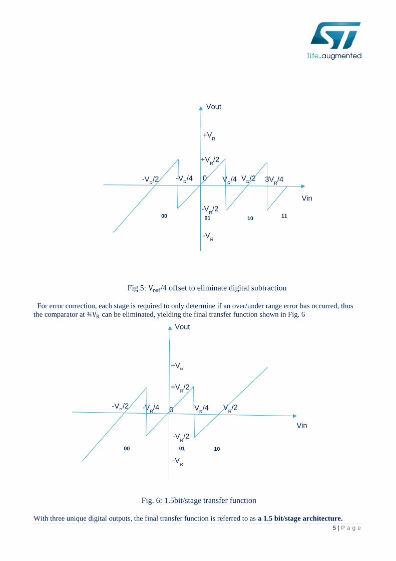
Subtraction can be eliminated by adding 1/2-leastsignificant-bit (LSB) offsets in both the ADC and DAC. The
ADSC offset uniformly shifts the location of the decision levels to the right by 1/2 LSB, and the DAC offset
shifts the x axis of the plot up by 1/2 LSB. If the DAC and SHA are ideal and the inter stage gain is 2, the
amplified residue (Fig. 5) remains within the conversion range of the next stage when the ADSC nonlinearity is
between ±1/2 LSB. Under these conditions, errors caused by the ADSC nonlinearity can be corrected, and the
correction requires either no change or addition. This is true because the offset introduced into the ADSC shifts
the decision levels to the right by 1/2 LSB, and if nonlinearity can shift them back to the left by no more than
this amount, the digital output is always less than or equal to its ideal value.
00 01 10 11
Vout
Vin
+VR
-VR
-3VR/4
-VR/2
-VR/4 0 V
R/4 V
R/2 3V
R/4
+VR/2
-VR/2
5 | P a g e
Fig.5: Vref/4 offset to eliminate digital subtraction
For error correction, each stage is required to only determine if an over/under range error has occurred, thus
the comparator at ¾VR can be eliminated, yielding the final transfer function shown in Fig. 6
Fig. 6: 1.5bit/stage transfer function
With three unique digital outputs, the final transfer function is referred to as a 1.5 bit/stage architecture.
00 01 10
Vin
+VR
-VR
-VR/2
-VR/4 0 V
R/4 V
R/2
+VR/2
-VR/2
11
3VR/4
Vout
00 01 10
Vin
+VR
-VR
-VR/2 -V
R/4 0 V
R/4 V
R/2
+VR/2
-VR/2
Vout

6 | P a g e
1.5 BIT/STAGE PIPELINE ARCHITECTURE:
1.5 bit/stage architecture requires only two comparators in the ADSC of each stage, and the comparator offset
up to ± VR/4 can be tolerated without degradation of the overall linearity or SNR. This is illustrated with
residue plots in Fig. 7. Input and output ranges of each stage are both ±VR. Fig. 7 shows ideal case with zero
comparator offsets and also the shifted residue plot due to the comparator offset ∆V. With the use of digital
correction algorithm in 1.5 b/stage pipeline architecture, the overflow of present stage output from the input
range of the following stage can be prevented even with the presence of a large comparator offset up to ± VR/4,
so that this offset error amplified down the pipeline can be detected for correction.
This large error correction range can also eliminate the dedicated input SH circuit. Instead, the input signal can
be sampled simultaneously by the switched capacitor amplifier and by the dynamic comparators of the flash
A/D section in the first stage. This is made possible by the fact that digital correction allows comparator errors
up to ± VR/4 without degradation of linearity or SNR.
Fig.7 Residue curve with & without comparator offset ∆V
Let us discuss the operation of pipeline ADC considering a 3 bit ADC. A 3 bit ADC consists of one 1.5 bit
ADC & one 2 bit FADC . The input range is ± V𝑅. The 1.5 bit ADC (First stage ADC) have 2 decision levels
(-V𝑅/4 & V𝑅/4 ) and 3 possible output codes, 00, 01, and 10 . The DACOUT is –V𝑅/2, 0, V𝑅/2 for DAC
I/P 00, 01 & 10 respectively. The Second Stage ADC (2 bit FADC) have 3 decision levels (-V𝑅/2, 0 &V𝑅/2) & 4
possible output codes 00, 01, 10 & 11.
Assuming Input = -0.2V𝑅 , The 1.5 bit ADC will provide o/p code 01 , The residue is 2(VIN-DACOUT) which
is equal to -0.4V𝑅, for this the FADC will provide o/p code 01.
The final o/p = 2(01) + 01=one bit left shift of the Ist stage O/P + 2nd stage O/P =010 + 01=01
00 01 10
Vin
+VR
-VR
-VR/2 -V
R/4 0 V
R/4 V
R/2
+VR/2
-VR/2
Vout

7 | P a g e
Consider a situation in which –V𝑅/4 threshold is shifted to –V𝑅/4 + V𝑅/8 due to offset of the comparator , Now
for i/p of -0.2V𝑅 ,the 1.5 bit ADC will provide o/p code 00, The residue is 2(-0.2V𝑅+0.5V𝑅)=0.6V𝑅 , for this
the FADC will provide O/P code 11.
The Final O/P =2(00) + 11=11 i.e. the correct output , ir-respective of the comparator offset as long as offset is
less than ½ LSB of the stage resolution.
The implementation of each pipeline stage is shown in Fig. 8. Although a single-ended configuration is shown
for simplicity, the actual implementation was fully differential. A common, switched-capacitor implementation
was chosen, which operates on a two-phase clock.
During the first phase, the input signal is applied to the input of the sub-ADC, which has thresholds at V𝑅/4 and
–V𝑅/4. The input signal ranges from –V𝑅 to V𝑅 (differential). Simultaneously, Vi is applied to sampling
capacitors 𝐶𝑠 and 𝐶𝑓 . At the end of the first clock phase, Vi is sampled across 𝐶𝑠 and 𝐶𝑓 , and the output of
the sub-ADC is latched. During the second clock phase, 𝐶𝑓 closes a negative feedback loop around the op-amp,
while the top plate of 𝐶𝑠 is switched to the digital-to-analog converter (DAC) output. This configuration
generates the stage residue at V𝑜 . For 1.5 bit per stage, 𝐶𝑠 =𝐶𝑓
-VR
-VR
/4
VR/4
VR
00
01
10
-VR
-VR
/2
VR/2
VR
00
01
10
11
0
-VR
/2
0
VR
/2
2 BIT FADC THRESHOLD DACOUT 1.5 BIT ADC THRESHOLD

8 | P a g e
Fig. 8. Switched capacitor implementation of each pipeline stage
V𝑜 =2Vin- V𝑅 for Vin > V𝑅/4
=2Vin for -V𝑅/4≤Vin≤V𝑅/4
=2Vin+ V𝑅 for Vin< -V𝑅/4
The D/A function is performed by two equal capacitors. When the input signal is applied, each stage samples
and quantizes the signal to its per stage resolution of 1.5b (i.e.. 2 decision levels and 3 possible output codes,
00, 01, and 10 excluding 1 l), subtracts the quantized analog voltage from the signal by connecting the
bottom plate of capacitor 𝐶𝑠 to VDAC ( ±V𝑅 or o), and passes the residue to the next stage with amplification
for finer conversion.
Approximate mathematical relations for the n-bit overall resolution, m.5 -bit inter-stage resolution pipeline
ADC component are given by
Number of stages (1.5bit) = n-1
Namplifier =(n − 2 )
m
Ncomparator =n ( 2m+1 −2)
m
SUB ADC
-VR
/4 VR
/4
MUX
-VR
/2 VR
/2 0
Cf
Cs V
out
Vin

9 | P a g e
The above equation provides an approximation of the total number of MDAC amplifiers required for the n-bit
m.5 bit-per-stage ADC & total number of comparators required for all sub-ADCs. For a 10-bit 1.5-bit/stage
ADC, eight amplifiers & 19 comparators are required.
A block diagram of a typical 10 bit pipeline A/D converter is shown in Fig. 9. It consists of a cascade of 9
identical stages in which each stage performs a coarse quantization, a D/A function on the quantization result,
subtraction, and amplification of the remainder.
Fig. 9: Block diagram of 10 bit pipeline ADC
Each stage resolves two bits with a sub-ADC, subtracts this value from its input, and amplifies the resulting
residue by a gain of two. The resulting 18 bits are combined with digital correction to yield ten bits at the output
of the ADC.
Stage 1 Vin
Stage 2 Stage 9
2 bits
X2
+
ADC
2 bits
+
DIGITAL CORRECTION
2 bits
Residue
10 bits digital output
2 bits
Vin -
DAC

10 | P a g e
The resolution of 1.5 b/stage is chosen in this pipeline implementation mainly for the following two reasons.
The first reason is to maximize the bandwidth of the SH/Gain SC circuit which limits the overall conversion
rate. In order to perform fast inter stage signal processing, the output of operational amplifier in the SC circuit
has to settle in half the clock period to the given accuracy of each stage prior to the next stage sampling
instance. Since the bandwidth of the SC inter stage amplifier depends on it’s inter stage gain, choosing the per-
stage resolution which allows the low closed-loop gain configuration for fast settling is essential. With the
resolution of 1.5 b/stage, the closed-loop gain of only 2 allows configuration for low load capacitance
(composed of only two sampling capacitors of the next stage and input capacitance of two comparators in the
flash A/D section) and large feedback factor (of about 1/3), and as a result a large inter stage amplifier
bandwidth can be achieved compared to that of larger per-stage resolution (2-3 b/stage).
Also, the resolution of 1.5 b/stage allows large correction range for comparator offsets in the flash A/D
section. Only two comparators are required in the flash A/D section of each stage, and the comparator offset
up to ± V𝑅/4 can be tolerated without degradation of the overall linearity or SNR. 1.5 bit/stage facilitates the
use of dynamic comparators with large input offset. However, it is not necessarily the optimal choice for power
consumption primarily because of the higher amplifier count and higher proportion of amplifier consumption in
comparison to the other blocks (eight amplifiers for a 10-bit 1.5-bit/stage ADC), and the fact that amplifier
power consumption in switched capacitor circuits actually increases at reduced supply voltages. As the supply
voltage is scaled down, the voltage available to represent the signal is reduced; therefore, dynamic range
becomes an important issue. To maintain the same dynamic range on a lower supply voltage, the thermal noise
in the circuit must also be proportionately reduced. There exists, however, a tradeoff between noise and power
consumption. Because of this strong tradeoff, it will be shown that under certain conditions, the power
consumption will actually increase as the supply voltage is decreased.
The power in the circuit is the static bias current times the voltage supply
P ∝ I Vdd
If the OTA can be modeled as a single transistor, then the bias current is proportional to the transconductance
times the gate overdrive
I ∝ gm (Vgs − Vt)
The closed-loop bandwidth of the circuit must be high enough to achieve the desired settling accuracy at the
given sampling rate gm
𝐶 ∝ 𝑓𝑠
The dynamic range (DR) is proportional to the signal swing squared over the sampled 𝐾𝑇/𝐶 thermal noise. α
represents what fraction of the available voltage supply is being utilized
DR ∝ (𝛼𝑉𝑑𝑑)2
𝐾𝑇/𝐶
From these assumptions, it follows that for a given dynamic range and sampling rate, the power will be
inversely proportional to the supply voltage. Furthermore, the power is inversely proportional to the square of
fractional signal swing. To minimize power consumption, it is important to use circuits that maximize the
available signal swing α
P ∝ 𝑘𝑇. 𝐷𝑅. 𝑓𝑠. (Vgs − Vt)
α2𝑉𝑑𝑑
Also P ∝ 𝑘𝑇. ( SNthR)
α𝑉𝑑𝑑

11 | P a g e
For a given SNthR , OTA power consumption is inversely proportional to supply voltage using the same
CMOS technology. For a fixed SNthR , power consumption increases for both larger geometry CMOS
processes (due to lower MOS transistor transconductance parameter and higher device parasitics requiring
more supply current) and smaller geometry CMOS technologies (due to lower operating supply voltages
necessitating larger sampling capacitors in order to still meet desired SNthR in spite of compromised input
voltage swing)
The sampling (𝐶𝑠) and feedback capacitor (𝐶𝑓) sizes are determined by kT/C noise constraints. The input
referred noise is given by:
𝑉2𝑖𝑛,𝑟𝑚𝑠 = KT.
𝐶𝑠 + 𝐶𝑓 + 𝐶𝑜𝑝𝑎𝑚𝑝
(𝐶𝑠 + 𝐶𝑓)2
Where 𝐶𝑜𝑝𝑎𝑚𝑝 is the input capacitance of the Op-Amp. The total noise will be four time (twice due to
sampling & residue calculation, further twice due to differential architecture) of the above defined.
Higher inter-stage resolutions seems to reduce the power consumption for low-voltage ADCs, since the
MDAC amplifier count is reduced, but With the resolution of 2.5 b/stage, the closed-loop gain of 4 requires
higher load capacitance (composed of four sampling capacitors of the next stage and input capacitance of six
comparators in the flash A/D section) and smaller feedback factor (of about 1/4), and as a result amplifier
bandwidth is reduced to half as compared to 1.5bit/stage. In order to have same order of BW, OPAMP current
will be increased by more than double. The unity gain frequency (𝑓𝑢) of opamp is related to 𝑓𝑠 , feedback factor
(β) & N bit settling and It is described as follows:
𝑓𝑢 =(N ln 2 )𝑓𝑠
𝛽𝜋
Where N ln2 is the Number of time constants for N bit settling.
For 3.5-bit/stage resolution, comparators will need to be preceded by continuous time preamplifiers to reduce
the effect of clock feed-through and switch charge injection on the signal and reference voltages. These
preamplifiers are designed for low gain (<10) and comparable SR with the inter-stage amplifiers. For 3.5-
bit/stage resolutions, auto-zeroing comparators are required to meet the higher accuracy requirements
consuming more power.
One approach to reduce power dissipation is to REDUCE THE CAPACITOR SIZES as the stage number
increases, since KT/C noise requirements become relaxed down the pipeline stages.
Another possible low-power approach is to reduce the number of amplifiers in a pipelined converter by
SHARING OF AMPLIFIER across stages using double sampling. Since, there is no requirement to sample
the amplifier offset when the input is sampled, as amplifier offset no longer cause linearity errors in the A/D
converter. Instead, they simply cause an input-referred offset voltage. As a result, the amplifier is idle during
sampling phase. Taking advantage of this, we can time-share the amplifier with the adjacent stage in the
pipeline.

12 | P a g e
Nonlinearities in Pipelined Analog to Digital Converters Sub-ADC nonlinearities and op-amp offset can be compensated by digital error correction techniques and offset
cancellation techniques, respectively. However, nonlinearity in the D/A sub converter and gain error in the
inter-stage amplifier remain as the main contributors to the converter’s overall nonlinearity.
To explain the effects of non-idealities on the pipelined A/D converter, we use a 2-b pipelined stage as an
example and assume the following stages have infinite resolution. Fig.10 shows the input-output relationship
and overall A/D conversion characteristic for an ideal 2-b pipelined stage.
The transition position is determined by the A/D sub-converter decision points, while the magnitude of the
transition at each code boundary is determined by the D/A sub-converter and the gain of the inter-stage
amplifier. The A/D sub-converter decision points are 0 and ±𝑉𝑅/2 and the corresponding D/A sub-converter
output levels are ±𝑉𝑅/4 and ±3𝑉𝑅/4 respectively. The stage gain is 4.
Gain error in the inter-stage amplifier causes the output to be either larger or smaller than the conversion range
of the following stage depending on whether the gain is larger or smaller, respectively, than the ideal gain. This
results in positive DNL (non-monotonicity) in the case of positive gain error and negative DNL (missing
codes) in the case of negative gain error. Fig. 10 shows the effect of the gain error on the pipelined input-output
relationship and overall A /D conversion characteristic.
-VR -V
R /2 0 V
R /2 V
R Vin
A/D converter o/p
Negative DNL(gain too small)

13 | P a g e
Fig. 10: Effects of inter-stage gain error.
For N bit linearity, the minimum required dc gain (A) of the OPAMP should be greater than (2)𝑁−1.
The opamp has to be stable with enough GM/PM at 20 log (1/β) not at 0dB. The available BW of the OPAMP
is also at 20 log (1/β) gain frequency.
Advantages & Limitations of the Pipeline ADC: The main advantages of pipelined ADC’s are that they can provide high throughput rates and occupy small die
areas. Both advantages stem from the concurrent operation of the stages; that is, at any time, the first stage
operates on the most recent sample while all other stages operate on residues from previous samples. The
associated latency is not a limitation in many applications. The main limitation of the pipelined ADC is the
power consumption. The main contributor of the power consumption is the opamp. The BW requirement
increases with the increase in Speed (𝑓𝑠) & decrease in feedback factor (β).In 1.5 bit per stage design for N bit
ADC, feedback factor is 1/2, and the number of amplifiers is N-2. If we choose 2.5 bit per stage architecture for
N bit ADC, the number of amplifiers is less i.e. (N-2)/2 but the feedback factor is now ¼ so the BW
requirement is doubled so current consumption is doubled. Also the number of comparators is increased. As a
result no power advantage in increasing number of bits per stage.
Amplifier sharing between stages is one of the techniques to reduce the power consumption. Design of High
gain (2)𝑁−1& High BW opamp with minimum power consumption is the most critical part of the pipelined
ADC. When the resolution increases, the cap sizes increases due to thermal noise limitation, as a result cap load
to opamp increases which results in more power required for OPAMP to achieve the performance.
Conclusion: The paper described about the Design of pipeline ADC starting from basic 2 bit per stage architecture with its
limitations, reason for choosing 1.5 bit per stage ,offset correction , concerns related to increase in number of
bits per stage, noise calculations, OPAMP gain & BW requirements, techniques to reduce power consumption
& its Nonlinearities .
-VR
-VR
/2
0 VR
/2 VR
Vin
A/D converter o/p
Positive DNL(gain too large)
-VR
/2