determination of the optical properties of individual gold
TRANSCRIPT

Determination of the Optical Properties of IndividualGold Nanorods Through Numerical Modelling andExperiment
Yevgeniy Davletshin1, Dr. Joseph C. Kumaradas1
1Ryerson University, Toronto, ON, Canada
Abstract
The optical scattering and absorption of gold nanorods (GNRs) depends on its size, shape, andsurroundings. This dependence is due to both intrinsic and extrinsic effects. A good understandingof this dependence is needed for applications of GNRs in photo-thermal therapy, optical and opto-acoustic imaging, biosensing, and other photonic areas. Extrinsic effects are caused by theproduction of localized and surface plasmons and are well understood through Mie theory forspherical particles and Maxwell's equations for arbitrary objects. Intrinsic effects become prominentat the nano-scale, when the cluster size becomes comparable or smaller than the bulk mean free pathof electrons between collisions and additional scattering of the conduction electrons from the clustersurface occur. The addition of this scattering will shorten the mean free path between collisions andincrease the damping constant. The increased damping is due to radiative losses in the case of goldnanoparticles larger than 20 nm in diameter and surface scattering in the case of smallernanoparticles. The surface scattering effect is quantified using a surface scattering parameter, A [1]and Leff=4V/S (V is the volume and S is the surface of the object) [2]. Surface scattering parameterA affects full width at half maximum of the surface plasmon resonance and usually used as a fittingparameter between theory and experiment. The surface scattering parameter for silica coated GNRsis not known. We will report on its measurement for silica coated GNRs using a combination ofspatial modulation spectroscopy (SMS) [3], transmission electron microscopy (TEM), and numericalmodeling using the finite element method (FEM). Individual silica coated gold GNRs weredeposited on a TEM grid (made of silica) (Figure 1a) and SMS (Figure 1b,c) was used toquantitatively determine the absorption cross-section of three individual GNRs. TEM was used toimage dimensions of the three GNRs (Figure 1d). The numerical model was built using COMSOLMultiphysics 3.5a to solve for the total electric field and to simulate the experimental setup of SMStechnique (Figure 2). The incident electric field, Einc, propagated in the downward direction (Figure2b) with a polarization in the left/right direction (along longitudinal axis of the nanorod). In order toobtain a stable solution, at least 10 linear elements per wavelength were used during meshing of thegeometries with further refinement inside of the nanorod (Figure 3a). The theoretical calculations ofthe absorption cross-section of the three GNRs were made using the modified bulk dielectricfunction of gold with inclusion of the electron surface scattering effect [2]. The experimental dataand numerical calculations were used to determine A for each GNR (Figure 4). The three valuesobtained were A1= 0.47, A2= 0.46 and A3 = 0.55, suggesting a universal value of A = 0.5 forsilica coated GNRs. The dependence of the dielectric function of gold nanoparticles on size/shape

can be quantitatively determined by combining SMS and correlated TEM of measurements ofsize/shape with numerical modeling, assuming Leff is quantitatively known.
Reference
1. Uwe Kreibig and Michael Vollmer, Optical Properties of Metal Clusters (Springer, 1995)2. Eduardo A. Coronado and George C. Schatz, “Surface plasmon broadening for arbitrary shapenanoparticles: A geometrical probability approach,” Journal of Chemical Physics 119, 3926–3934(2003)3. Otto L. Muskens, et. al., “Quantitative absorption spectroscopy of a single gold nanorod”,Journal of Physical Chemistry C 112, 8917–8921 (2008).
Figures used in the abstract
Figure 1: (a) TEM grid with 50e-6×50e-6 m windows, (b) an image of TEM window from SMSnanoscope, (c) a zoom-in view (1.5e-6×1.5e-6 m window) of a gold nanorod from the SMSnanoscope. Color bar is an arbitrary scale that corresponds to the light transmission change due tothe absorption of the light by the imaged particle. (d) 3 TEM images of single gold nanorods coatedwith silica shells.

Figure 2: (a) Schematic of single nanorod, showing the various dimensions obtained from TEMimaging; (b) a 2D projection of the 3D geometry and boundary conditions of the computationalmodel. The model was truncated at the top and bottom using an absorbing boundary condition(ABC), at the left and right with a perfect electric conductor (PEC), and at the front and back with aperfect magnetic conductor (PMC). The incident wave was polarized on the left-right direction,travelling downward. Therefore an additional absorbing layer, known as a perfectly matched layer(PML) was placed at the bottom of the domain. The medium inside the domain was air (n = 1), andthe TEM grid was modeled as a silica layer (n = 1.46). In the computational model a = 2.4e-6 m, b= 0.4e-6 m, c = 1.4e-6 m, and d = 40 nm. The domain in the front-to-back direction had a size equalto c.
Figure 3: Single silica coated GNR model. (a) Mesh quality; (b) Electric field distribution (log|E|);(c) Scattered Electric field distribution (log|Esca|).
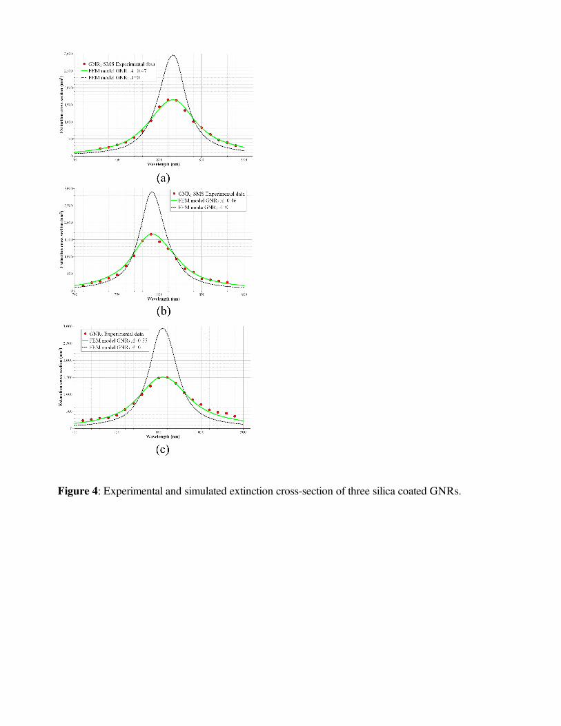
Figure 4: Experimental and simulated extinction cross-section of three silica coated GNRs.