development of an fmcw ladar source chip using mems
TRANSCRIPT
Development of an FMCW LADAR Source Chip using MEMS-Electronic-Photonic Heterogeneous Integration
Niels Quack1, James Ferrara1, Simone Gambini1, Sangyoon Han1, Christopher Keraly1, Pengfei Qiao2, Yi Rao1, Phillip Sandborn1, Li Zhu1, Shun-Lien Chuang2, Eli Yablonovitch1,
Bernhard Boser1, Connie Chang-Hasnain1, Ming C. Wu1 1University of California, Berkeley, USA, 2University of Illinois at Urbana-Champaign, USA
Abstract: We present a modular integration platform, combining active and passive photonic devices with CMOS integrated electronics. Based on this integration platform, an integrated Frequency Modulated Continuous Wave (FMCW) Laser Detection and Ranging (LADAR) source chip is being developed. Such a LADAR source chip can be used in miniaturized 3D imaging systems for defense and consumer electronics applications. In this paper, we discuss the integration approach, the performance of select individual components, and experimental results on a bench top LADAR model system.
Keywords: Frequency Modulated Continuous Wave (FMCW); Laser Detection and Ranging (LADAR); Light Detection and Ranging (LIDAR); Micro-Electro-Mechanical System (MEMS); III-V semiconductor; tunable Vertical Cavity Surface Emitting Laser (VCSEL); Optoelectronic Phase Locked Loop (OPLL); CMOS; Silicon Photonics; 3D Integration; 3D Imaging; Short Wavelength Infrared (SWIR).
Introduction 3D imaging systems have recently obtained increased publicity by their use in consumer electronics devices. In 2011, the Kinect motion sensor by Microsoft has become one of the fastest selling consumer electronics devices. 3D imaging systems, originally developed for military applications, are used in prototypes of civilian autonomous cars, such as the google self-driving car. While the Kinect uses stereoscopic imaging [1, 2], most LIDAR systems for autonomous cars are based on Time of Flight (TOF) measurement [3]. These systems are usually several cm3 in size and offer 10s of cm ranging resolutions at an object distance of 10m [4]. For better ranging resolutions, high speed detectors and electronics are required. A third approach consists in FMCW LADAR. Bench top systems have recently been demonstrated using MEMS tunable lasers [5]. This approach allows for better range resolution at smaller distances, without the need of high speed electronics. 31 µm range resolution at 1.5m has recently been reported [6].
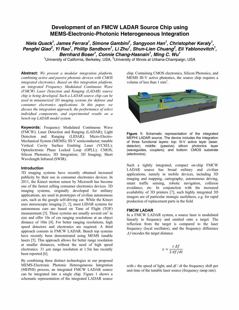
By combining three distinct technologies in our proposed MEMS-Electronic Photonic Heterogeneous Integration (MEPHI) process, an integrated FMCW LADAR source can be integrated into a single chip. Figure 1 shows a schematic representation of the integrated LADAR source
chip. Containing CMOS electronics, Silicon Photonics, and MEMS III-V active photonics, the source chip requires a volume of less than 1 mm3.
Figure 1: Schematic representation of the integrated MEPHI LADAR source. The device includes the integration of three functional layers: top: III-V active layer (laser, detector), middle: (passive) silicon photonics layer (waveguides, couplers); and bottom: CMOS substrate (electronics).
Such a tightly integrated, compact on-chip FMCW LADAR source has broad military and civilian applications, namely in mobile devices, including 3D imaging and mapping, cartography, autonomous driving, smart traffic sensing, robotic navigation, collision avoidance, etc. In conjunction with the increased availability of 3D printers [7], such highly integrated 3D imagers are of particular strategic usefulness, e.g. for rapid production of replacement parts in the field.
FMCW LADAR In a FMCW LADAR system, a source laser is modulated linearly in frequency and emitted onto a target. The reflection from the target is compared to the laser frequency (local oscillator), and the frequency difference f encodes the target distance
with c the speed of light, and df / dt the frequency shift per unit time of the tunable laser source (frequency ramp rate).
𝑥 =𝑐 𝛥𝑓
2 𝑑𝑓/𝑑𝑡

In the proposed LADAR chip, the frequency ramp is generated using an optoelectronic feedback loop, with a tunable MEMS VCSEL a center wavelength of 1.55um. In this short wavelength infrared (SWIR) range, high powers can be used for increased ranging distances and signal quality, while being eye safe, and imaging through humidity saturated environments such as clouds and fogs are possible.
Linear Frequency Sweep Generation In order to generate the FMCW LADAR source signal, a linear frequency sweep is generated using an optoelectronic feedback circuit, described by Satyan et al. [8].
The schematic representation of the operating principle of the FMCW LADAR source is shown in Fig. 3. The active III-V tunable VCSEL (red) generates a frequency swept signal, which is fed into a Silicon Photonics Mach-Zehnder-Interferometer (MZI) (blue). The linearly swept signal produces a sinusoidal output at the detector, which is beaten with a reference oscillator to produce a dc signal. In the CMOS circuit (black), the dc part is integrated to form a linear ramp, which is then squared (‘predistortion circuit’), in order to account for the nonlinear tuning characteristics of the electrostatically tuned MEMS VCSEL. A linear ramp is thus a self-consistent solution to this opto-electronic feedback circuit as described by Satyan et al. [8]. The loop integrator can be reset at the desired repetition frequency of the frequency chirp to produce a saw-tooth shaped output form, or using adequate signal processing, a triangular output waveform can be obtained. A separate feedback loop is implemented for amplitude control.
Integration Strategy The modular MEPHI integration platform is schematically depicted in Figure 2. Three distinct technologies are integrated into a single chip: active III-V (MEMS tunable VCSELs with high-index-contrast grating (HCG) mirrors) [9], Silicon Photonics (photodetectors, silicon photonic
waveguides, couplers, and interferometers) [10], and CMOS electronics (phase locked loop, temperature compensation, signal processing).
Figure 3: Circuit diagram representing the Optoelectronic Phase Locked Loop (OPLL) generating a broadband frequency chirp. The integration of the three different component system is represented in red (III-V), blue (Silicon Photonics) and black (CMOS electronics).
The advantage of this integration strategy is the optimization of the components individually, and the independence of the three technologies. With this strategy, the highly optimized capabilities for CMOS foundries can leveraged, as well as the increasingly available Silicon Photonics technology from foundries.
As shown in Figure 2, the integration requires wafer level bonding technologies [11] and Through Silicon Vias (TSV) for electrical and thermal interconnect between the three layers.
Figure 2: Fabrication process for system integration and cross section of the integrated MEPHI LADAR source.
Fabrication Process:
• Silicon Photonics (SiP) and integrated electronics (CMOS)
wafers from foundry shuttle runs and/or wafer runs
• III-V stack and MEMS HCG processed on Indium Phosphide
(InP) wafer in the Berkeley Marvell Nanolab
• Wafer bonding of Silicon Photonics to CMOS, backside CMP
• Through Silicon Via (TSV) and contact opening
• III-V wafer alignment and bonding to SiP/CMOS wafer stack,
electrical contacting, wirebonding

Tunable MEMS VCSEL The frequency modulated signal is generated using a MEMS tunable Vertical Cavity Surface Emitting Laser (VCSEL). Fig. 4 shows a schematic representation of the VCSEL structure.
Figure 4: Schematic representation of a MEMS tunable VCSEL. A suspended High Contrast Grating (HCG) serves as movable reflector. Electrostatic actuation allows tuning of the lasing wavelength.
The VCSEL frequency is controlled by changing the cavity length of the laser by electrostatic tuning of a MEMS high contrast grating (HCG). In this configuration, the HCG is designed to be a highly reflective mirror [9]. The low mass of such a sub wavelength grating reflector allows very high tuning speed. Resonance frequencies above MHz have been demonstrated [12]
Fig. 5 shows a SEM image of a tunable VCSEL fabricated for this project.
Figure 5: SEM image of a fabricated MEMS tunable VCSEL.
The VCSELs are typically tunable over a wide range: 15nm (mechanical tuning via electrostatic MEMS actuation), plus 11nm (current tuning) have been reported (Fig. 6).
Figure 6: Tuning characteristics of a tunable VCSEL using high contrast grating MEMS reflectors. Using both MEMS tuning and thermal (current) tuning, 26.3nm tuning has been achieved.
Linear Frequency Ramp using tunable VCSEL
Using the proposed MEPHI process allows integration of the optoelectronic phased lock loop (OPLL) generating a saw-tooth shaped VCSEL output frequency. Here, we report on the implementation of the optoelectronic feedback loop in a bench top model using an electrostatically actuated tunable VCSEL, fiber optic components and a Field Programmable Gate Array (FPGA) for signal processing, as represented in Figure 7. In essence, the FPGA contains mixing with a reference oscillator, an integrator and a pre distortion circuit. In difference to the OPLL presented in [8], we invert the ramp slope at the desired repetition frequency, in order to generate a triangular waveform, rather than a saw tooth shaped form. This configuration takes into account the continuous tuning characteristic of the MEMS HCG mirror.
Figure 7: Bench top model OPLL for LADAR frequency ramp generation using fiber optic and discrete components. Setting the interferometer delay to 200ps, using a 75kHz reference frequency, and setting the repetition rate to 0.8ms, the OPLL generated a linear frequency triangular ramp signal with a total VCSEL frequency excursion of 150 GHz. Figure 8 shows the OPLL in unlocked and locked state, generating the frequency swept FMCW LADAR signal.
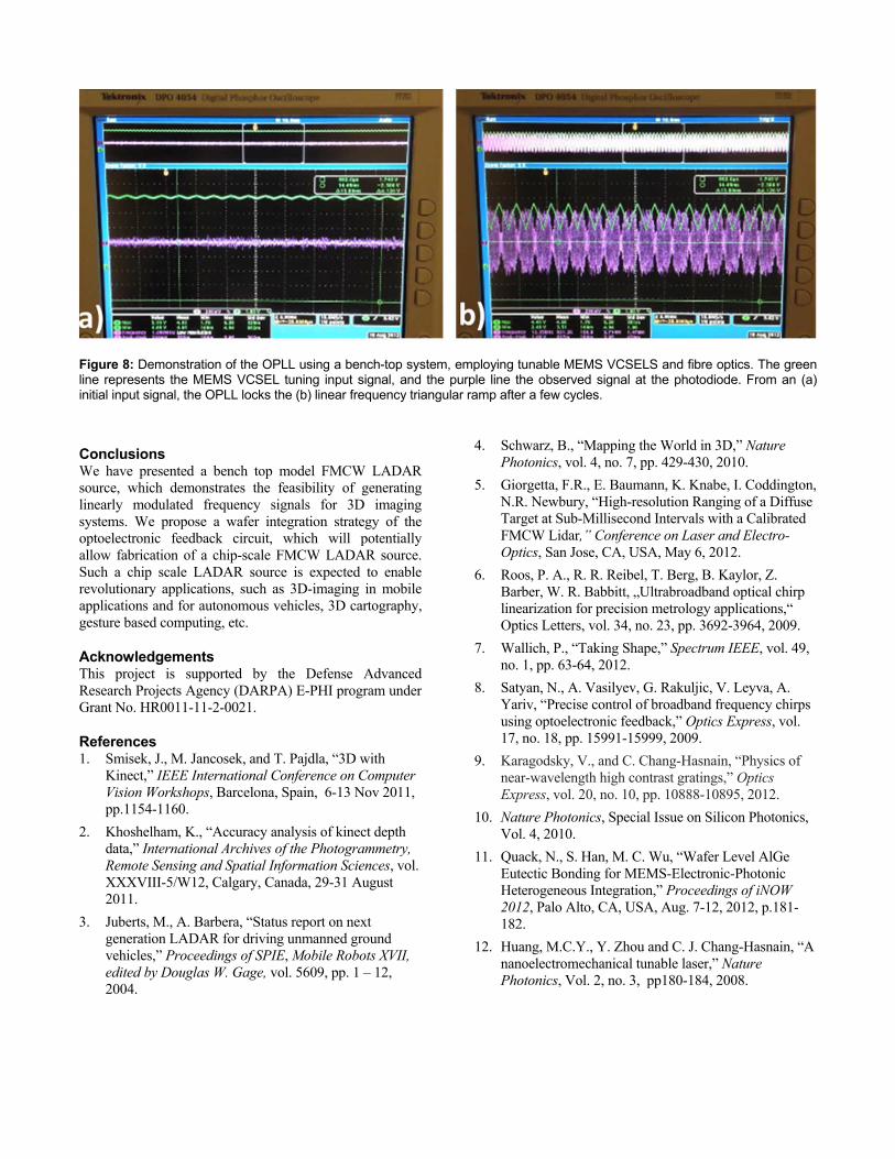
Figure 8: Demonstration of the OPLL using a bench-top system, employing tunable MEMS VCSELS and fibre optics. The green line represents the MEMS VCSEL tuning input signal, and the purple line the observed signal at the photodiode. From an (a) initial input signal, the OPLL locks the (b) linear frequency triangular ramp after a few cycles.
Conclusions We have presented a bench top model FMCW LADAR source, which demonstrates the feasibility of generating linearly modulated frequency signals for 3D imaging systems. We propose a wafer integration strategy of the optoelectronic feedback circuit, which will potentially allow fabrication of a chip-scale FMCW LADAR source. Such a chip scale LADAR source is expected to enable revolutionary applications, such as 3D-imaging in mobile applications and for autonomous vehicles, 3D cartography, gesture based computing, etc.
Acknowledgements This project is supported by the Defense Advanced Research Projects Agency (DARPA) E-PHI program under Grant No. HR0011-11-2-0021.
References 1. Smisek, J., M. Jancosek, and T. Pajdla, “3D with
Kinect,” IEEE International Conference on Computer Vision Workshops, Barcelona, Spain, 6-13 Nov 2011, pp.1154-1160.
2. Khoshelham, K., “Accuracy analysis of kinect depth data,” International Archives of the Photogrammetry, Remote Sensing and Spatial Information Sciences, vol. XXXVIII-5/W12, Calgary, Canada, 29-31 August 2011.
3. Juberts, M., A. Barbera, “Status report on next generation LADAR for driving unmanned ground vehicles,” Proceedings of SPIE, Mobile Robots XVII, edited by Douglas W. Gage, vol. 5609, pp. 1 – 12, 2004.
4. Schwarz, B., “Mapping the World in 3D,” Nature Photonics, vol. 4, no. 7, pp. 429-430, 2010.
5. Giorgetta, F.R., E. Baumann, K. Knabe, I. Coddington, N.R. Newbury, “High-resolution Ranging of a Diffuse Target at Sub-Millisecond Intervals with a Calibrated FMCW Lidar,” Conference on Laser and Electro-Optics, San Jose, CA, USA, May 6, 2012.
6. Roos, P. A., R. R. Reibel, T. Berg, B. Kaylor, Z. Barber, W. R. Babbitt, „Ultrabroadband optical chirp linearization for precision metrology applications,“ Optics Letters, vol. 34, no. 23, pp. 3692-3964, 2009.
7. Wallich, P., “Taking Shape,” Spectrum IEEE, vol. 49, no. 1, pp. 63-64, 2012.
8. Satyan, N., A. Vasilyev, G. Rakuljic, V. Leyva, A. Yariv, “Precise control of broadband frequency chirps using optoelectronic feedback,” Optics Express, vol. 17, no. 18, pp. 15991-15999, 2009.
9. Karagodsky, V., and C. Chang-Hasnain, “Physics of near-wavelength high contrast gratings,” Optics Express, vol. 20, no. 10, pp. 10888-10895, 2012.
10. Nature Photonics, Special Issue on Silicon Photonics, Vol. 4, 2010.
11. Quack, N., S. Han, M. C. Wu, “Wafer Level AlGe Eutectic Bonding for MEMS-Electronic-Photonic Heterogeneous Integration,” Proceedings of iNOW 2012, Palo Alto, CA, USA, Aug. 7-12, 2012, p.181-182.
12. Huang, M.C.Y., Y. Zhou and C. J. Chang-Hasnain, “A nanoelectromechanical tunable laser,” Nature Photonics, Vol. 2, no. 3, pp180-184, 2008.