development of the depfet sensor with signal compression ...€¦ · pietsch9, e. quartieri10, v....
TRANSCRIPT
1
SRI Workshop Zurich, 06.07.12
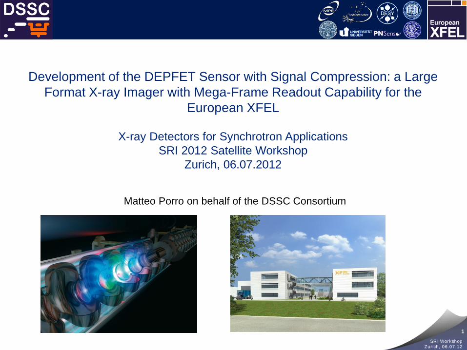
Development of the DEPFET Sensor with Signal Compression: a Large Format X-ray Imager with Mega-Frame Readout Capability for the
European XFEL
X-ray Detectors for Synchrotron Applications SRI 2012 Satellite Workshop
Zurich, 06.07.2012 Matteo Porro on behalf of the DSSC Consortium
2
SRI Workshop Zurich, 06.07.12
M. Porro1,2, L. Andricek2,3, S. Aschauer8, L. Bombelli4,5, A. Castoldi4,5, G. De Vita1,2, I. Diehl7, F. Erdinger6, S. Facchinetti4,5, C. Fiorini4,5, P. Fischer6, T. Gerlach6, H. Graafsma7, C. Guazzoni4,5, K. Hansen7, H. Hirsemann7, P. Kalavakuru7, A. Kugel6, P. Lechner8, G. Lutz8, M. Manghisoni10, D. Mezza4,5, D. Moch1,2, U. Pietsch9, E. Quartieri10, V. Re10, C. Reckleben7, C. Sandow8, S. Schlee1,2, J. Soldat6, L. Strueder1,2, A. Wassatsch2,3, G. Weidenspointner1,2, C. Wunderer7
1) Max Planck Institut fuer Extraterrestrische Physik, Garching, Germany 2) MPI Halbleiterlabor, Muenchen, Germany 3) Max Planck Institut fuer Physik, Muenchen, Germany 4) Dipartimento di Elettronica e Informazione, Politecnico di Milano, Milano, Italy 5) Sezione di Milano, Italian National Institute of Nuclear Physics (INFN), Milano, Italy 6) Zentrales Institut für Technische Informatik, Universitaet Heidelberg, Heidelberg, Germany 7) Deutsches Elektronen-Synchrotron DESY, Hamburg, Germany 8) PNSensor GmbH, Muenchen, Germany 9) Fachbereich Physik, Universitaet Siegen, Siegen, Germany 10) Dipartimento di ingegneria industriale, Università di Bergamo, Bergamo, Italy
DSSC Consortium
3
SRI Workshop Zurich, 06.07.12
Introduction
DSSC Concept overview • Requirements and Design Parameters • Focal Plane overview • Non-linear DEPFET working principle • Readout ASIC
Experimental results
System simulation Conclusions
Outline

4
SRI Workshop Zurich, 06.07.12
5
SRI Workshop Zurich, 06.07.12
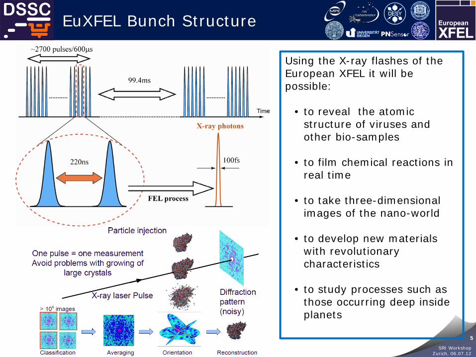
EuXFEL Bunch Structure
Using the X-ray flashes of the European XFEL it will be possible:
• to reveal the atomic
structure of viruses and other bio-samples
• to film chemical reactions in real time
• to take three-dimensional
images of the nano-world • to develop new materials
with revolutionary characteristics
• to study processes such as those occurring deep inside planets

6
SRI Workshop Zurich, 06.07.12
2D detectors for EuXFEL
Three Detector Developments at the European XFEL (coordinator: M. Kuster) Adaptive Gain Pixel integrating Pixel Detector Consortium (AGIPD)
(Project Leader: H. Graafsma) o DESY o PSI / SLS Villingen o Universität Hamburg o Universität Bonn
Large Pixel Detector Consortium (LPD)
(Project Leader: M. French) o Rutherford Appleton Laboratory / STFC o University of Glasgow
DEPFET Sensor with Signal Compression Consortium (DSSC)
(Project Leader: M. Porro) o Max Planck Halbleiterlabor Munich o DESY o Universität Heidelberg o Politecnico di Milano / INFN o Università di Bergamo o Universität Siegen

7
SRI Workshop Zurich, 06.07.12
DSSC – Design Parameters
Parameter
Energy range optimized for 0.5 … 6 keV
Number of pixels 1024 x 1024 Sensor Pixel Shape Hexagonal Sensor Pixel pitch ~ 204 x 236 µm2
Dynamic range / pixel / pulse
~5000 ph @ 0.5 keV > 10000 ph @ E≥1 keV
Resolution Single photon detection also @ 0.5 keV
Frame rate 0.9-4.5 MHz Stored frames per Macro bunch ≥ 640
Operating temperature
-20˚C optimum, RT possible
1 Mpixel camera with: • Single photon sensitivity
event at 0.5 keV
• high-dynamic range (>10000 ph/pixel)
• Frame rate up to 4.5 MHz (1 image every 220 ns)
All the properties have to be achieved simultaneously DSSC will be the first instrument to fulfill this requirement

8
SRI Workshop Zurich, 06.07.12
DSSC Overview - Concept
● DEPFET Active Pixel Sensor
● Readout Concept
Fast analog shaping Immediate 8 Bit digitization (9 bit for f ≤ 2.2 MHz) In-Pixel SRAM Readout during macro bunch gaps
● Power cycling
Focal Plane

9
SRI Workshop Zurich, 06.07.12
• 1024x 1024 pixels
• 16 ladders/hybrid boards
• 32 monolithic sensors 128x256 6.3x3 cm2
• DEPFET Sensor bump bonded to 8 Readout ASICs (64x64 pixels)
• 2 DEPFET sensors wire bonded to a hybrid board connected to regulator modules
• Dead area: ~15%
x-y Gap
128 x 256 Pixel Sensor
21 c
m (1
024
pixe
ls)
DSSC Overview- Focal Plane Overview
10
SRI Workshop Zurich, 06.07.12
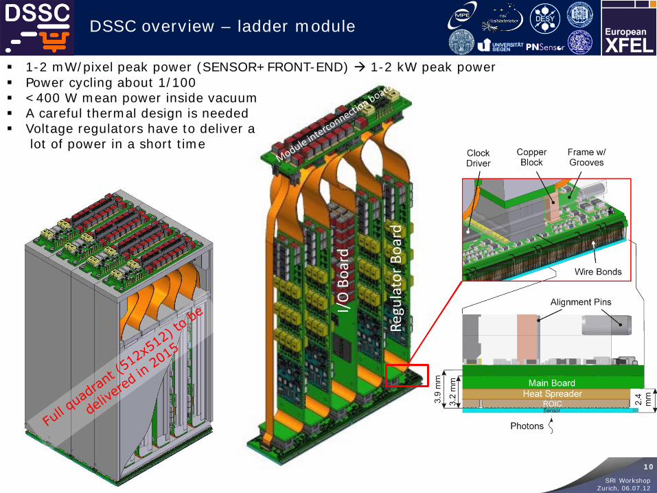
DSSC overview – ladder module
~3 mm
1-2 mW/pixel peak power (SENSOR+FRONT-END) 1-2 kW peak power Power cycling about 1/100 <400 W mean power inside vacuum A careful thermal design is needed Voltage regulators have to deliver a
lot of power in a short time
I/O
Boa
rd
Regu
lato
r Boa
rd
11
SRI Workshop Zurich, 06.07.12
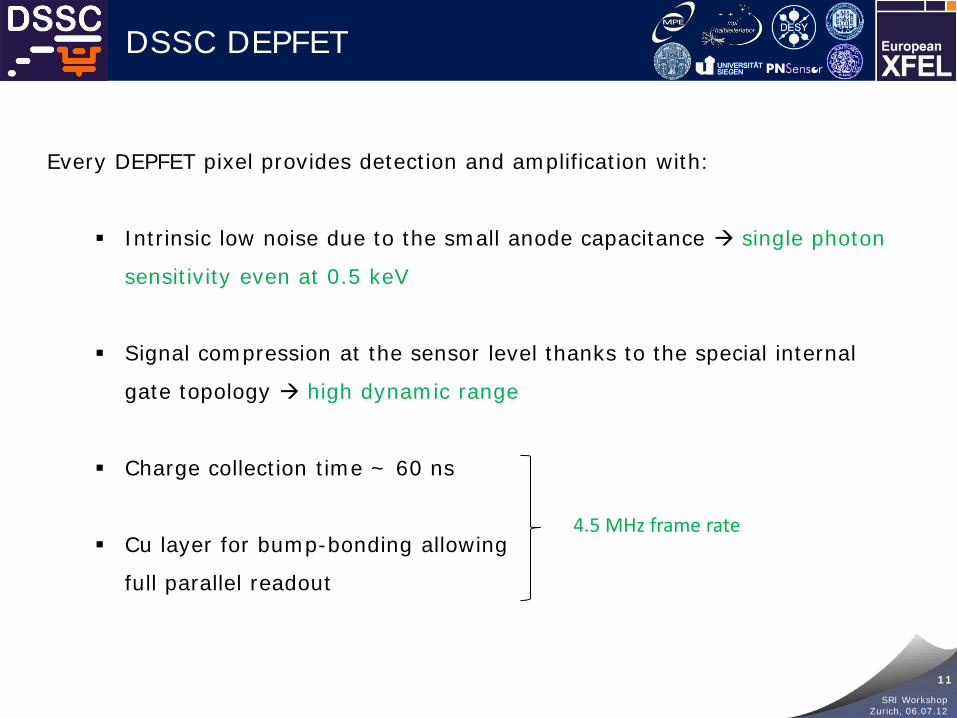
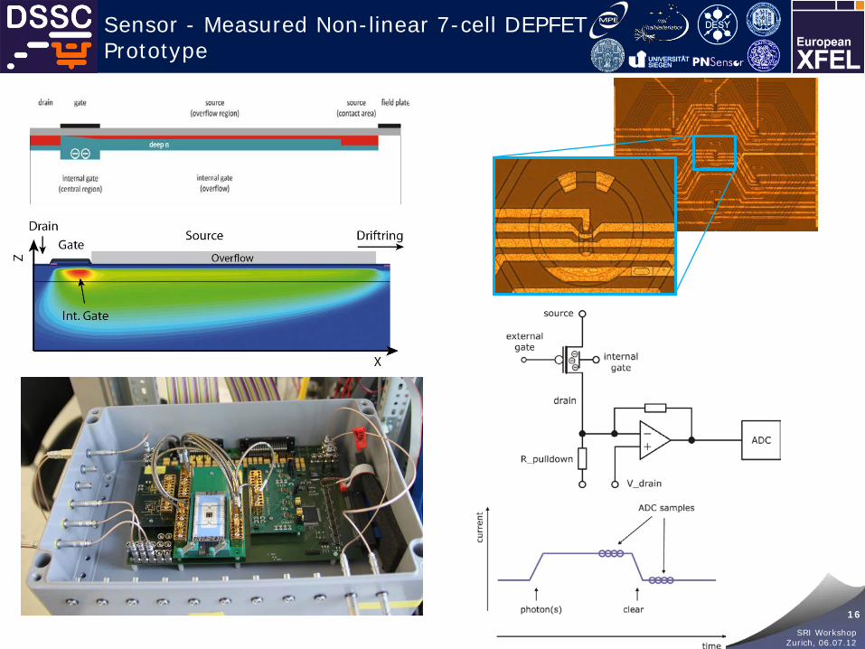
DSSC DEPFET
4.5 MHz frame rate
Every DEPFET pixel provides detection and amplification with:
Intrinsic low noise due to the small anode capacitance single photon
sensitivity even at 0.5 keV
Signal compression at the sensor level thanks to the special internal
gate topology high dynamic range
Charge collection time ~ 60 ns
Cu layer for bump-bonding allowing
full parallel readout
12
SRI Workshop Zurich, 06.07.12
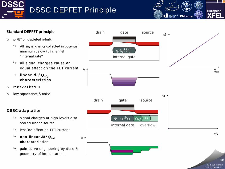
DSSC DEPFET Principle
Standard DEPFET principle
o p-FET on depleted n-bulk
All signal charge collected in potential minimum below FET channel
"internal gate"
all signal charges cause an equal effect on the FET current
linear ΔI/Qsig characteristics
o reset via ClearFET
o low capacitance & noise
DSSC adaptation
signal charges at high levels also stored under source
less/no effect on FET current
non-linear ΔI/Qsig characteristics
gain curve engineering by dose & geometry of implantations
13
SRI Workshop Zurich, 06.07.12
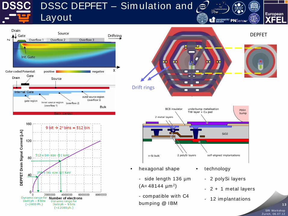
DSSC DEPFET – Simulation and Layout
236
µm
272 µm Pitchx: 204 µm Pitchy: 236 µm
DEPFET
Drift rings
• hexagonal shape
- side length 136 µm (A=48144 µm2)
- compatible with C4 bumping @ IBM
• technology
- 2 polySi layers
- 2 + 1 metal layers
- 12 implantations

14
SRI Workshop Zurich, 06.07.12
DSSC overview - ASIC
Every ASIC pixel comprises in 206 x 236 µm: • A trapezoidal analog filter (optimum filter for white series noise) • A single slope 8 bit ADC (9 bit for f≤2.2 MHz) • An SRAM able to store ≥640 frames
Gain and offset can be adjusted pixel-wise
Single slope ADC ASIC final format : 64 x 64 pixels 130 nm CMOS Process C4 Bumps

15
SRI Workshop Zurich, 06.07.12
MAIN ACHIEVEMENTS (on sensor and readout ASIC)
16
SRI Workshop Zurich, 06.07.12
Sensor - Measured Non-linear 7-cell DEPFET Prototype
17
SRI Workshop Zurich, 06.07.12
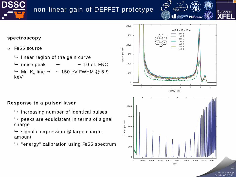
spectroscopy
o Fe55 source
linear region of the gain curve noise peak ~ 10 el. ENC Mn-Kα line ~ 150 eV FWHM @ 5.9
keV
Response to a pulsed laser
increasing number of identical pulses peaks are equidistant in terms of signal
charge signal compression @ large charge
amount "energy" calibration using Fe55 spectrum
non-linear gain of DEPFET prototype

18
SRI Workshop Zurich, 06.07.12
non-linear gain DEPFET (pxd-7)
signal compression
o seven cells of a cluster
o standard variant (W/L = 25/3)
o sensitivity in the linear region
gq ≈ 600 pA/el.
o compression factor
~ 17.5
o current dispersion
ΔI/I ≈ 10 %
non-linear vs. spectroscopy type DEPFET
o equal gate dimensions
W/L = 25/3
o performance at small energy
equal within sample-to-sample variation
o spectroscopy-type DEPFET stays linear
19
SRI Workshop Zurich, 06.07.12
13sep11
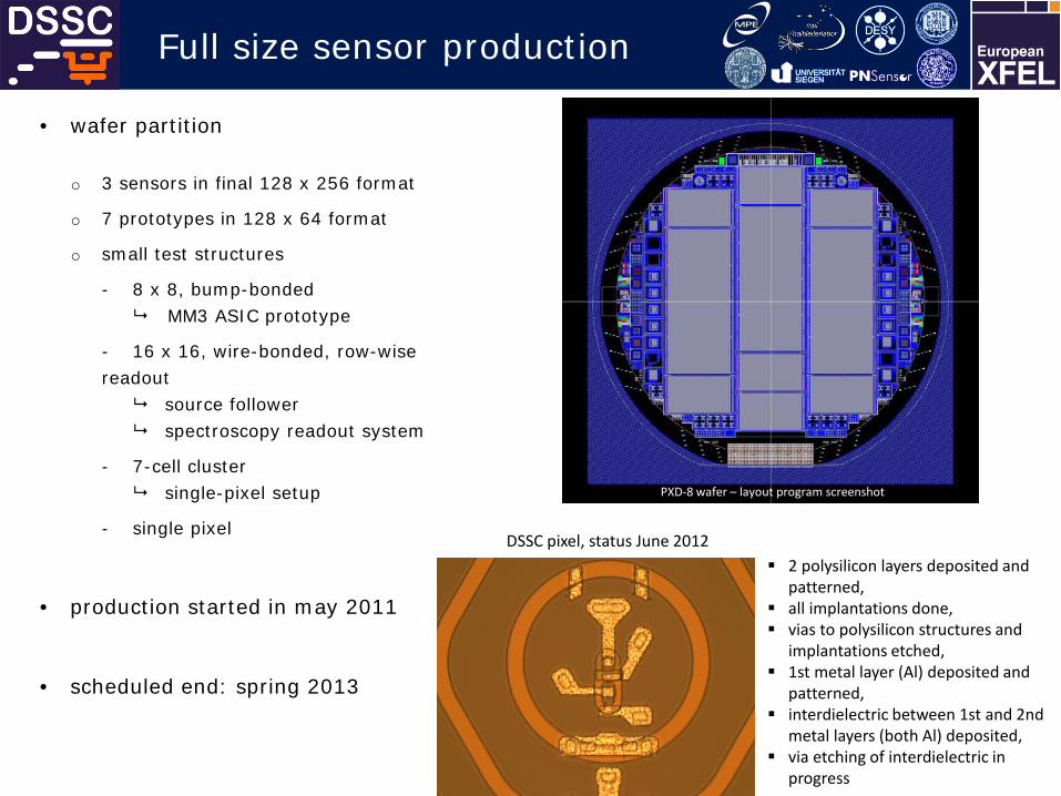
• wafer partition
o 3 sensors in final 128 x 256 format
o 7 prototypes in 128 x 64 format
o small test structures
- 8 x 8, bump-bonded MM3 ASIC prototype
- 16 x 16, wire-bonded, row-wise readout
source follower spectroscopy readout system
- 7-cell cluster single-pixel setup
- single pixel
• production started in may 2011
• scheduled end: spring 2013
PXD-8 wafer – layout program screenshot
Full size sensor production
DSSC pixel, status June 2012 2 polysilicon layers deposited and
patterned, all implantations done, vias to polysilicon structures and
implantations etched, 1st metal layer (Al) deposited and
patterned, interdielectric between 1st and 2nd
metal layers (both Al) deposited, via etching of interdielectric in
progress
20
SRI Workshop Zurich, 06.07.12
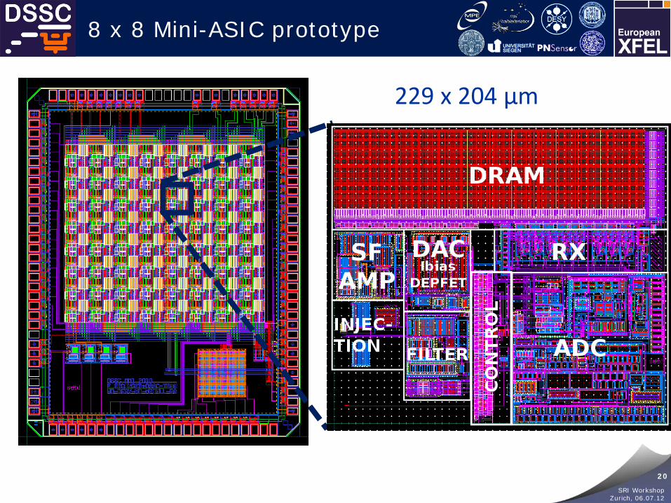
8 x 8 Mini-ASIC prototype
229 x 204 µm

21
SRI Workshop Zurich, 06.07.12
ASIC: test on individual blocks
● Individual test structures have been tested with dedicated setups
● Measurements on the analog front-end connected to a standard DEPFET have been performed
13.0 el
1 MHz
22
SRI Workshop Zurich, 06.07.12
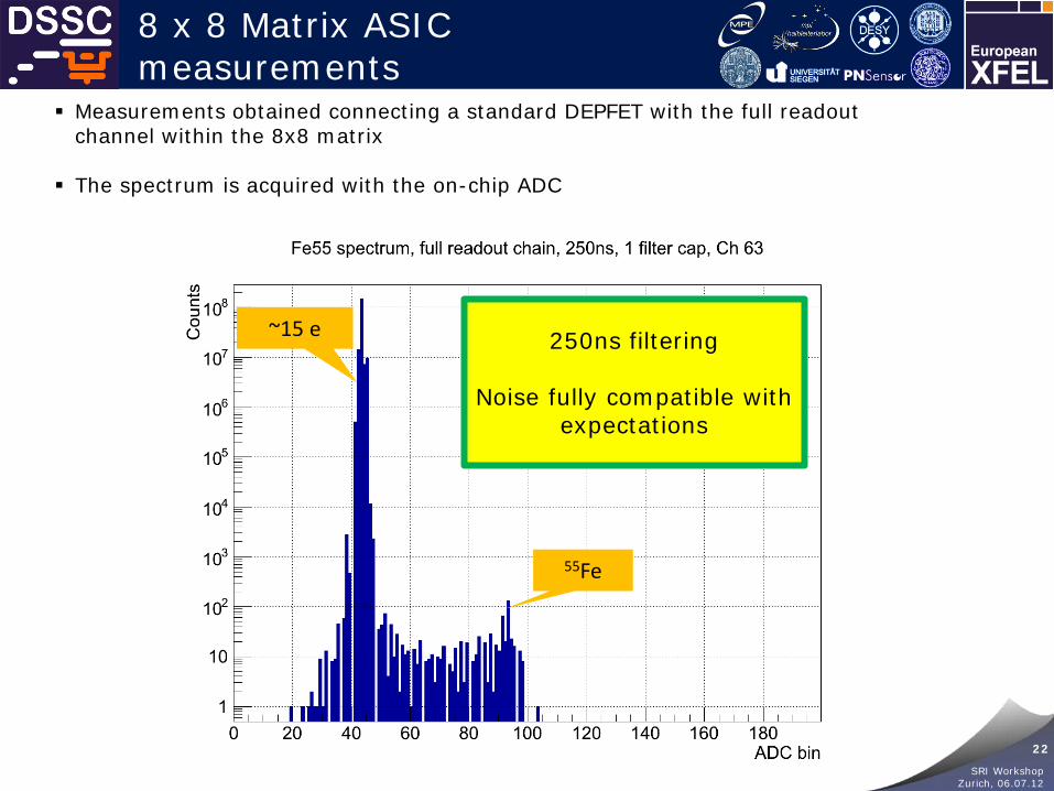
~15 e 250ns filtering
Noise fully compatible with expectations
55Fe
8 x 8 Matrix ASIC measurements
Measurements obtained connecting a standard DEPFET with the full readout channel within the 8x8 matrix
The spectrum is acquired with the on-chip ADC
23
SRI Workshop Zurich, 06.07.12
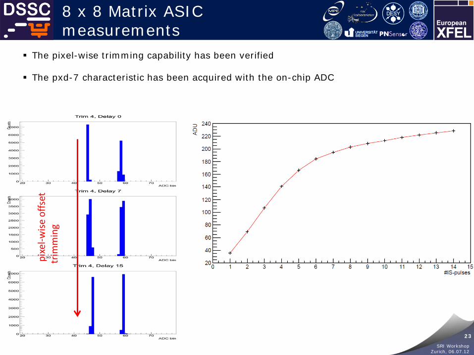
8 x 8 Matrix ASIC measurements
pix
el-w
ise o
ffset
tr
imm
ing
The pixel-wise trimming capability has been verified
The pxd-7 characteristic has been acquired with the on-chip ADC
24
SRI Workshop Zurich, 06.07.12
System Simulation
25
SRI Workshop Zurich, 06.07.12
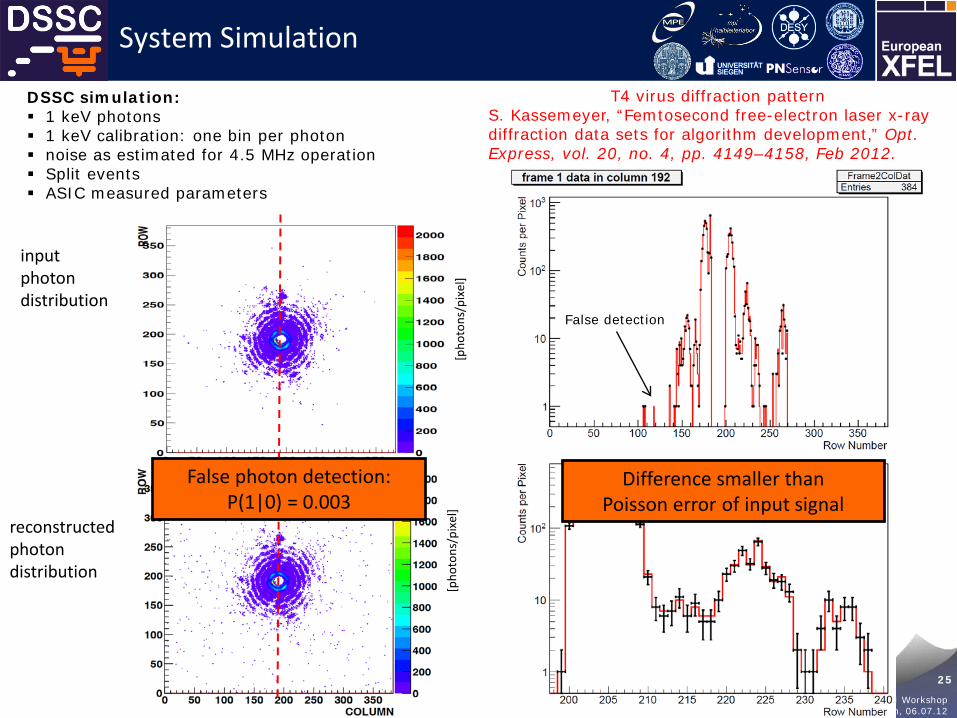
DSSC simulation: 1 keV photons 1 keV calibration: one bin per photon noise as estimated for 4.5 MHz operation Split events ASIC measured parameters
[pho
tons
/pix
el]
[pho
tons
/pix
el]
input photon distribution
reconstructed photon distribution
System Simulation
T4 virus diffraction pattern S. Kassemeyer, “Femtosecond free-electron laser x-ray diffraction data sets for algorithm development,” Opt. Express, vol. 20, no. 4, pp. 4149–4158, Feb 2012.
False photon detection: P(1|0) = 0.003
False detection
Difference smaller than Poisson error of input signal

26
SRI Workshop Zurich, 06.07.12
Increased single photon resolution with limited dynamic range
1 keV photons Number of
bins attributed to the first
photon
Frame Rate 0.9 MHz 2.2 MHz 4.5 MHz
8 bits 9 bits 8 bits 9 bits 8 bits 9 bits
1 2370 12080 2370 12080 2370 NA 2 453 2360 453 2360 NA NA 3 162 905 162 905 NA NA
1 keV photons Number of
bins attributed to the first
photon
Frame Rate 0.9 MHz 2.2 MHz 4.5 MHz
8 bits 9 bits 8 bits 9 bits 8 bits 9 bits
1 3.3x10⁻⁵ 2.1x10⁻² 3.3x10⁻⁵ 2.1x10⁻² 2.7x10⁻³ NA 2 3.8x10⁻¹⁴ 3.3x10⁻⁵ 1.4x10⁻¹⁰ 3.3x10⁻⁵ NA NA 3 1.5x10⁻²⁵ 2.0x10⁻⁹ 8.9x10⁻¹¹ 1.0x10⁻⁸ NA NA
Dynamic range in Photons
P (1|0)
At 1 keV with 2 bins/photon it is possible to achieve a dynamic range of about 500 ph. and a P(1|0)≈4x10-14
Gain settings can be switched on the fly during the experiment
27
SRI Workshop Zurich, 06.07.12
Summary & Conclusions
We are developing a Pixel Detector system for the European XFEL based on innovative non-linear DEPFET devices
In our fully parallel readout scheme, the signals coming from the pixels
are filtered, digitized and stored in the focal plane
The DEPFET signal compression principle has been experimentally verified
An 8x8 readout ASIC comprising the whole pixel readout chain has been produced and tested. The noise measured coupling the ASIC with a standard DEPFET is of 15 el. r.m.s. With an integration time of 250 ns. This value is fully compatible with the expected performance of the DSSC.
Estimations based on the first experimental result show that it will be
possible to achieve single photon detection and high dynamic range also for low energies.
The first DSSC Sensor production comprising full-size sensors has
started. One working quadrant (512 x 512 ) will be available in 2015
The full camera will be available in the middle of 2017

28
SRI Workshop Zurich, 06.07.12
Thank You