diffusion and intermetallics formation between pd ag...
TRANSCRIPT
Materials Science and Engineering B57 (1999) 116–126
Diffusion and intermetallics formation between Pd/Agmetallization and Sn/Pb/Ag solder in surface mount solder joints
G.Y. Li, Y.C. Chan *Department of Electronic Engineering, City Uni6ersity of Hong Kong, 83 Tat Chee A6enue, Kowloon, Hong Kong
Received 24 March 1998; received in revised form 12 September 1998
Abstract
Interdiffusion and intermetallics formation between metallization conductor Pd–Ag and solder 62Sn-36Pb-2Ag have beenstudied. Silver and palladium dot mapping images of solder joints demonstrate that the Pd–Ag metallization layer graduallydisappears after 11 days of ageing. It is observed that silver-rich areas exist in the bulk of the 62Sn-36Pb-2Ag solder after ageingbut palladium-rich areas are not evident. The diffusion coefficient of the silver in the solder joints for this material system wasmeasured. The activation energy and pre-exponential factor for the silver diffusion were found to be about 0.475 eV and0.56×10-10 m2 s−1, respectively for the configuration of surface mount thick film solder joints studied. X-ray diffraction resultsreveal the formation of the intermetallic compounds Ag5Sn, Ag3Sn, Pd3Sn2, Pd2Sn, PdSn2, PdSn4, PdSn, PbPd3, and Pb3Pd5.© 1999 Published by Elsevier Science S.A. All rights reserved.
Keywords: Interdiffusion; Intermetallics; Joint; Metallization; Solder
1. Introduction
Thick film hybrid circuit technology is widely used inhybrid microelectronics. In this technology, a metalliza-tion pattern is printed on the ceramic substrate to formthe circuit pattern. Ag/Pd-based conductors are proba-bly the most commonly used alloy systems in thick filmhybrid circuits [1]. The screen printing process is usedto apply the material for conductors, resistors, andsolder onto the ceramic substrate. The conductor mate-rial is held within an organic binder which contains aglass frit to bond the metallic conductor to the ceramicsubstrate during the sintering process. A similar processapplies for the resistors. The solder, which is in theform of a paste consisting of solder particles and a fluxbinder, is screen-printed over selected conductor pads.
Components to be soldered to the assembly are thenplaced on the solder-coated conductor pads. A reflow-soldering process is then used utilising condensation(vapour phase) or infra-red techniques. The conductormaterial should be wetted satisfactorily by the solder/flux combination, but should not be leached away(dissolved) into the solder.
One of the main factors that affects reliability of athick film solder joint is the interaction of the Pd/Agconductor metallization with Pb/Sn solder. Some inves-tigations of element diffusion, intermetallics formation,and the effects of temperature cycling tests on solderjoint adhesion strength have been done previously [2–6]. The results show that swelling in the conductor filmdue to the volume change associated with elementinterdiffusion between the solder and the conductorand formation of intermetallics during soldering andservice life, decreases the adhesion strength between thesolder and the conductor. However, the interface reac-tions between the conductor metallization layer and thesolder and especially the effects of thermal ageing at an* Corresponding author.
0921-5107/99/$ - see front matter © 1999 Published by Elsevier Science S.A. All rights reserved.
PII: S0921 -5107 (98 )00313 -4
G.Y. Li, Y.C. Chan / Materials Science and Engineering B57 (1999) 116–126 117
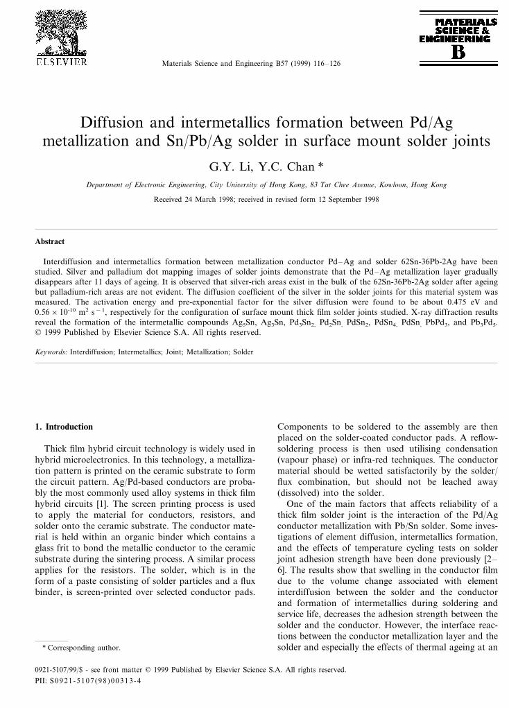
Fig. 1. Backscattered SEM picture and X-ray elements mapping of a cross sectional view of a solder joints before ageing.
elevated temperature for real industrial assemblies arenot yet well understood. Further understanding of thekinetics of the solid-state diffusion in the solder joints isvery important for the electronics industry. This investi-gation aims at observing the interfacial reactions be-tween the solder and metallisation layer and especiallythe effect of thermal ageing at an elevated temperatureon the solid-state diffusion between a Pd–Ag metallisedlayer and 62Sn-36Pb-2Ag solder alloy. The data mayfind useful application in industry.
2. Experimental procedure
Commercial DuPont Pd/Ag (weight ratio: 1:3) con-
ductor 6120 was printed on a 96% Al2O3 substrate(Kyocera, Japan) to form the electric circuit using thickfilm printing technology. After drying at 150°C for 10min, the samples were air fired in a belt furnace. Thetotal firing cycle time was 30 min with 10 min of peakfiring at a temperature of 850°C. Surface mount passivecomponents were then assembled on the substrates bymeans of standard infrared reflow using solder paste62Sn-36Pb-2Ag (Electro-Science Laboratories, USA).
Separate test samples were aged isothermally in anoven at 70, 100, and 150°C for periods of 0, 2, 5, 11, 20,32, and 47 days. The metallographic preparation of thesolder joints was done according to the method de-scribed in our previous work [7]. The microstructure ofthe solder joints of the specimens was investigated with
G.Y. Li, Y.C. Chan / Materials Science and Engineering B57 (1999) 116–126118
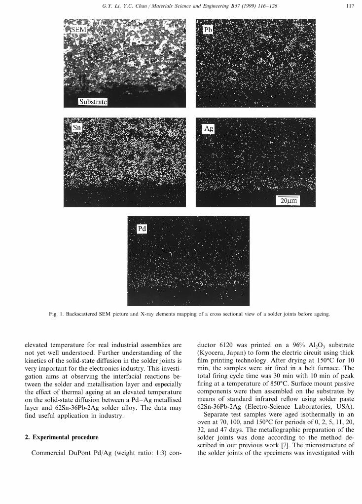
Fig. 2. Backscattered SEM picture and X-ray elements mapping of a cross sectional view of a solder joints after 2 days ageing at 150°C.
a scanning electron microscope (SEM JSM-820).X-ray element dot mapping was used to characterizethe element interdiffusion at the interface of theconductor metallization and solder. Element diffusiondepth measurements were taken from the samples, themean of 10 readings taken at different locations oneach sample being recorded. An X-ray diffractometer(XRD Siemens D500) was employed to investigatethe composition of the intermetallics.
3. Results and discussions
3.1. Microstructure of solder joints
Backscattered SEM micrographs and X-ray element
mapping for lead, tin, silver, and palladium of crosssections of a surface mount solder joint before ageingare shown in Fig. 1. The silver and palladium dotmapping demonstrates that a distinct layer of metalliza-tion conductor remains next to the ceramic substrate.The thickness of the metallization layer was approxi-mately 10 mm.
SEM micrographs and X-ray element mapping forsurface mount solder joints aged at 150°C for differenttimes are presented in Figs. 2–7. There is evident tindiffusion into the Pd/Ag conductor. It is observed thatthe diffusing tin reaches the conductor/substrate inter-face after 120 h of ageing. The silver and palladiumX-ray mapping reveals that the longer the ageing timethe more serious the silver and palladium diffusion intothe solder, with the silver diffusion rate somewhat lower
G.Y. Li, Y.C. Chan / Materials Science and Engineering B57 (1999) 116–126 119
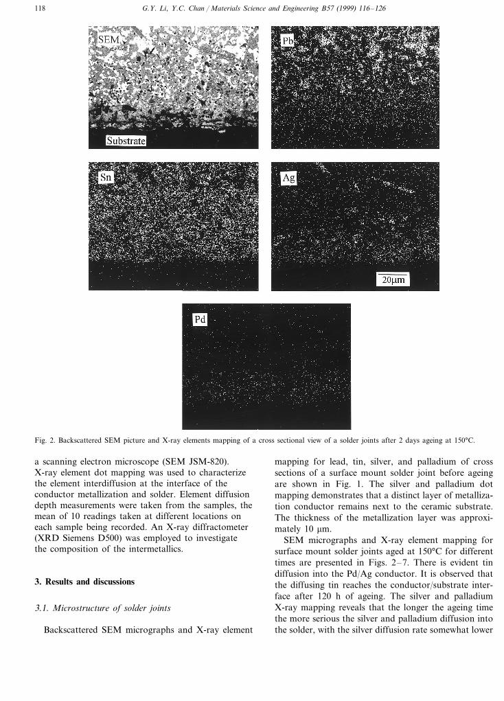
Fig. 3. Backscattered SEM picture and X-ray elements mapping of a cross sectional view of a solder joints after 5 days ageing at 150°C.
than the palladium. Further work is required to under-stand the diffusion mechanism for this.
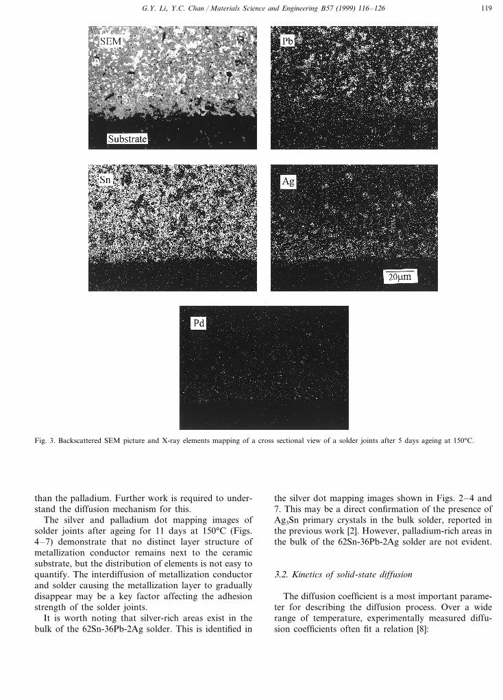
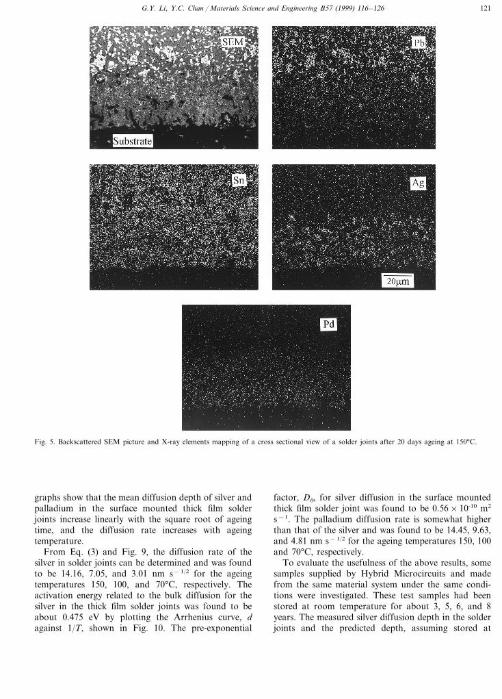
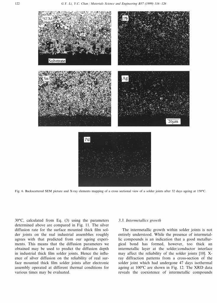
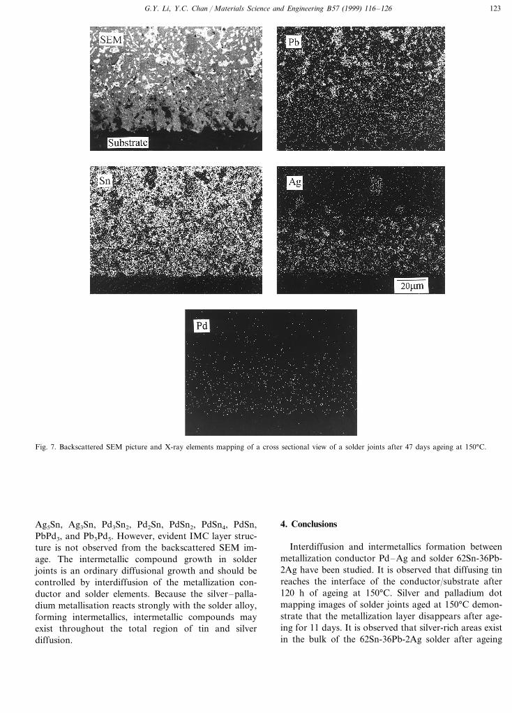
The silver and palladium dot mapping images ofsolder joints after ageing for 11 days at 150°C (Figs.4–7) demonstrate that no distinct layer structure ofmetallization conductor remains next to the ceramicsubstrate, but the distribution of elements is not easy toquantify. The interdiffusion of metallization conductorand solder causing the metallization layer to graduallydisappear may be a key factor affecting the adhesionstrength of the solder joints.
It is worth noting that silver-rich areas exist in thebulk of the 62Sn-36Pb-2Ag solder. This is identified in
the silver dot mapping images shown in Figs. 2–4 and7. This may be a direct confirmation of the presence ofAg3Sn primary crystals in the bulk solder, reported inthe previous work [2]. However, palladium-rich areas inthe bulk of the 62Sn-36Pb-2Ag solder are not evident.
3.2. Kinetics of solid-state diffusion
The diffusion coefficient is a most important parame-ter for describing the diffusion process. Over a widerange of temperature, experimentally measured diffu-sion coefficients often fit a relation [8]:

G.Y. Li, Y.C. Chan / Materials Science and Engineering B57 (1999) 116–126120
Fig. 4. Backscattered SEM picture and X-ray elements mapping of a cross sectional view of a solder joints after 11 days ageing at 150°C.
D=D0exp(−Q/kT) (1)
where: k is the Boltzmann constant and T is the abso-lute temperature. Both Q and the pre-exponential fac-tor D0 are independent of temperature. Q and D0
depend on the identity of the diffusing element andthe composition of the matrix crystal. External forcesand pressure can also affect Q and D0. Eq. (1) iscalled the Arrhenius equation for diffusion.By defini-tion, the experimental quantity Q is given by
Q= −k( ln D((1/T)
(2)
and is called the experimental activation energy.
The relationship between the diffusion depth andageing time for the one-dimensional diffusion is con-sidered to have the usual form [9]:
d=2Dt (3)
That is, the diffusion depth d is proportional tosquare root of time t.
To determine the diffusion parameters, the diffusiondepth of silver and palladium in all solder joints wasmeasured. The observed diffusional direction is alongthe direction perpendicular to the substrate. The rela-tionships between mean diffusion depth and squareroot of ageing time are plotted in Figs. 8 and 9. The
G.Y. Li, Y.C. Chan / Materials Science and Engineering B57 (1999) 116–126 121
Fig. 5. Backscattered SEM picture and X-ray elements mapping of a cross sectional view of a solder joints after 20 days ageing at 150°C.
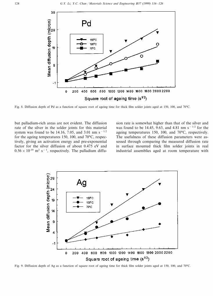
graphs show that the mean diffusion depth of silver andpalladium in the surface mounted thick film solderjoints increase linearly with the square root of ageingtime, and the diffusion rate increases with ageingtemperature.
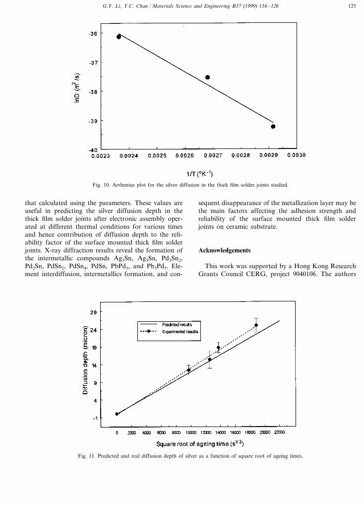
From Eq. (3) and Fig. 9, the diffusion rate of thesilver in solder joints can be determined and was foundto be 14.16, 7.05, and 3.01 nm s−1/2 for the ageingtemperatures 150, 100, and 70°C, respectively. Theactivation energy related to the bulk diffusion for thesilver in the thick film solder joints was found to beabout 0.475 eV by plotting the Arrhenius curve, dagainst 1/T, shown in Fig. 10. The pre-exponential
factor, D0, for silver diffusion in the surface mountedthick film solder joint was found to be 0.56×10⁻¹⁰ m2
s−1. The palladium diffusion rate is somewhat higherthan that of the silver and was found to be 14.45, 9.63,and 4.81 nm s−1/2 for the ageing temperatures 150, 100and 70°C, respectively.
To evaluate the usefulness of the above results, somesamples supplied by Hybrid Microcircuits and madefrom the same material system under the same condi-tions were investigated. These test samples had beenstored at room temperature for about 3, 5, 6, and 8years. The measured silver diffusion depth in the solderjoints and the predicted depth, assuming stored at
G.Y. Li, Y.C. Chan / Materials Science and Engineering B57 (1999) 116–126122
Fig. 6. Backscattered SEM picture and X-ray elements mapping of a cross sectional view of a solder joints after 32 days ageing at 150°C.
30°C, calculated from Eq. (3) using the parametersdetermined above are compared in Fig. 11. The silverdiffusion rate for the surface mounted thick film sol-der joints on the real industrial assemblies roughlyagrees with that predicted from our ageing experi-ments. This means that the diffusion parameters weobtained may be used to predict the diffusion depthin industrial thick film solder joints. Hence the influ-ence of silver diffusion on the reliability of real sur-face mounted thick film solder joints after electronicassembly operated at different thermal conditions forvarious times may be evaluated.
3.3. Intermetallics growth
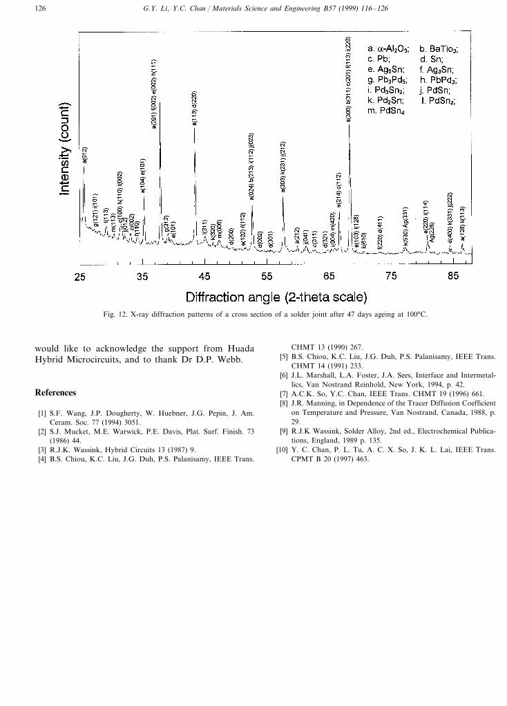
The intermetallic growth within solder joints is notentirely understood. While the presence of intermetal-lic compounds is an indication that a good metallur-gical bond has formed, however, too thick anintermetallic layer at the solder/conductor interfacemay affect the reliability of the solder joints [10]. X-ray diffraction patterns from a cross-section of thesolder joint which had undergone 47 days isothermalageing at 100°C are shown in Fig. 12. The XRD datareveals the coexistence of intermetallic compounds
G.Y. Li, Y.C. Chan / Materials Science and Engineering B57 (1999) 116–126 123
Fig. 7. Backscattered SEM picture and X-ray elements mapping of a cross sectional view of a solder joints after 47 days ageing at 150°C.
Ag5Sn, Ag3Sn, Pd3Sn2, Pd2Sn, PdSn2, PdSn4, PdSn,PbPd3, and Pb3Pd5. However, evident IMC layer struc-ture is not observed from the backscattered SEM im-age. The intermetallic compound growth in solderjoints is an ordinary diffusional growth and should becontrolled by interdiffusion of the metallization con-ductor and solder elements. Because the silver–palla-dium metallisation reacts strongly with the solder alloy,forming intermetallics, intermetallic compounds mayexist throughout the total region of tin and silverdiffusion.
4. Conclusions
Interdiffusion and intermetallics formation betweenmetallization conductor Pd–Ag and solder 62Sn-36Pb-2Ag have been studied. It is observed that diffusing tinreaches the interface of the conductor/substrate after120 h of ageing at 150°C. Silver and palladium dotmapping images of solder joints aged at 150°C demon-strate that the metallization layer disappears after age-ing for 11 days. It is observed that silver-rich areas existin the bulk of the 62Sn-36Pb-2Ag solder after ageing
G.Y. Li, Y.C. Chan / Materials Science and Engineering B57 (1999) 116–126124
Fig. 8. Diffusion depth of Pd as a function of square root of ageing time for thick film solder joints aged at 150, 100, and 70°C.
but palladium-rich areas are not evident. The diffusionrate of the silver in the solder joints for this materialsystem was found to be 14.16, 7.05, and 3.01 nm s−1/2
for the ageing temperatures 150, 100, and 70°C, respec-tively, giving an activation energy and pre-exponentialfactor for the silver diffusion of about 0.475 eV and0.56×10-10 m2 s−1, respectively. The palladium diffu-
sion rate is somewhat higher than that of the silver andwas found to be 14.45, 9.63, and 4.81 nm s−1/2 for theageing temperatures 150, 100, and 70°C, respectively.The usefulness of these diffusion parameters were as-sessed through comparing the measured diffusion ratein surface mounted thick film solder joints in realindustrial assemblies aged at room temperature with
Fig. 9. Diffusion depth of Ag as a function of square root of ageing time for thick film solder joints aged at 150, 100, and 70°C..
G.Y. Li, Y.C. Chan / Materials Science and Engineering B57 (1999) 116–126 125
Fig. 10. Arrhenius plot for the silver diffusion in the thick film solder joints studied.
that calculated using the parameters. These values areuseful in predicting the silver diffusion depth in thethick film solder joints after electronic assembly oper-ated at different thermal conditions for various timesand hence contribution of diffusion depth to the reli-ability factor of the surface mounted thick film solderjoints. X-ray diffraction results reveal the formation ofthe intermetallic compounds Ag5Sn, Ag3Sn, Pd3Sn2,Pd2Sn, PdSn2, PdSn4, PdSn, PbPd3, and Pb3Pd5. Ele-ment interdiffusion, intermetallics formation, and con-
sequent disappearance of the metallization layer may bethe main factors affecting the adhesion strength andreliability of the surface mounted thick film solderjoints on ceramic substrate.
Acknowledgements
This work was supported by a Hong Kong ResearchGrants Council CERG, project 9040106. The authors
Fig. 11. Predicted and real diffusion depth of silver as a function of square root of ageing times..
G.Y. Li, Y.C. Chan / Materials Science and Engineering B57 (1999) 116–126126
Fig. 12. X-ray diffraction patterns of a cross section of a solder joint after 47 days ageing at 100°C.
would like to acknowledge the support from HuadaHybrid Microcircuits, and to thank Dr D.P. Webb.
References
[1] S.F. Wang, J.P. Dougherty, W. Huebner, J.G. Pepin, J. Am.Ceram. Soc. 77 (1994) 3051.
[2] S.J. Mucket, M.E. Warwick, P.E. Davis, Plat. Surf. Finish. 73(1986) 44.
[3] R.J.K. Wassink, Hybrid Circuits 13 (1987) 9.[4] B.S. Chiou, K.C. Liu, J.G. Duh, P.S. Palanisamy, IEEE Trans.
CHMT 13 (1990) 267.[5] B.S. Chiou, K.C. Liu, J.G. Duh, P.S. Palanisamy, IEEE Trans.
CHMT 14 (1991) 233.[6] J.L. Marshall, L.A. Foster, J.A. Sees, Interface and Intermetal-
lics, Van Nostrand Reinhold, New York, 1994, p. 42.[7] A.C.K. So, Y.C. Chan, IEEE Trans. CHMT 19 (1996) 661.[8] J.R. Manning, in Dependence of the Tracer Diffusion Coefficient
on Temperature and Pressure, Van Nostrand, Canada, 1988, p.29.
[9] R.J.K Wassink, Solder Alloy, 2nd ed., Electrochemical Publica-tions, England, 1989 p. 135.
[10] Y. C. Chan, P. L. Tu, A. C. X. So, J. K. L. Lai, IEEE Trans.CPMT B 20 (1997) 463.
.