digital accelerometer data sheet adxl312 - analog · pdf filedigital accelerometer data sheet...
TRANSCRIPT
3-Axis, ±1.5 g/±3 g/±6 g/±12 g Digital Accelerometer
Data Sheet ADXL312
Rev. B Document Feedback Information furnished by Analog Devices is believed to be accurate and reliable. However, no responsibility is assumed by Analog Devices for its use, nor for any infringements of patents or other rights of third parties that may result from its use. Specifications subject to change without notice. No license is granted by implication or otherwise under any patent or patent rights of Analog Devices. Trademarks and registered trademarks are the property of their respective owners.
One Technology Way, P.O. Box 9106, Norwood, MA 02062-9106, U.S.A. Tel: 781.329.4700 ©2010–2017 Analog Devices, Inc. All rights reserved. Technical Support www.analog.com
FEATURES Ultralow power: as low as 57 µA in measurement mode and
0.1 µA in standby mode at VS = 3.3 V (typical) Power consumption scales automatically with bandwidth User-selectable resolution
Fixed 10-bit resolution Full resolution, where resolution increases with g range,
up to 13-bit resolution at ±12 g (maintaining 2.9 mg/LSB scale factor in all g ranges)
Embedded FIFO technology minimizes host processor load Built-in motion detection functions for activity/inactivity
monitoring Supply and I/O voltage range: 2.0 V to 3.6 V SPI (3- and 4-wire) and I2C digital interfaces Flexible interrupt modes mappable to either interrupt pin Measurement ranges selectable via serial command Bandwidth selectable via serial command Wide temperature range (−40 to +105°C) 10,000 g shock survival Pb free/RoHS compliant Small and thin: 5 mm × 5 mm × 1.45 mm LFCSP package Qualified for automotive applications
APPLICATIONS Car alarm Hill start aid (HSA) Electronic parking brake Data recorder (black box)
GENERAL DESCRIPTION The ADXL3121 is a small, thin, low power, 3-axis accelerometer with high resolution (13-bit) measurement up to ±12 g. Digital output data is formatted as 16-bit twos complement and is accessible through either a serial port interface (SPI) (3- or 4-wire) or I2C digital interface.
The ADXL312 is well suited for car alarm or black box applica-tions. It measures the static acceleration of gravity in tilt-sensing applications, as well as dynamic acceleration resulting from motion or shock. Its high resolution (2.9 mg/LSB) enables resolution of inclination changes of as little as 0.25°. A built-in FIFO facili-tates using oversampling techniques to improve resolution to as little as 0.05° of inclination.
Several special sensing functions are provided. Activity and inactivity sensing detects the presence or absence of motion and whether the acceleration on any axis exceeds a user-set level. These functions can be mapped to interrupt output pins. An integrated 32 level FIFO can be used to store data to minimize host processor intervention.
Low power modes enable intelligent motion-based power management with threshold sensing and active acceleration measurement at extremely low power dissipation.
The ADXL312 is supplied in a small, thin 5 mm × 5 mm × 1.45 mm, 32-lead, LFCSP package.
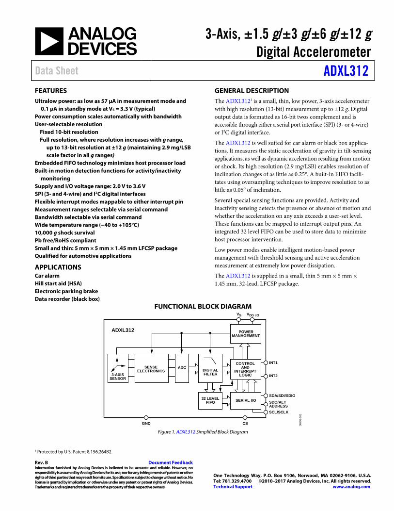
FUNCTIONAL BLOCK DIAGRAM
3-AXISSENSOR
SENSEELECTRONICS DIGITAL
FILTER
ADXL312 POWERMANAGEMENT
CONTROLAND
INTERRUPTLOGIC
SERIAL I/O
INT1
VS VDD I/O
INT2
SDA/SDI/SDIOSDO/ALTADDRESSSCL/SCLK
GND
ADC
32 LEVELFIFO
CS 0879
1-00
1
Figure 1. ADXL312 Simplified Block Diagram
1 Protected by U.S. Patent 8,156,264B2.
ADXL312 Data Sheet
Rev. B | Page 2 of 32
TABLE OF CONTENTS Features .............................................................................................. 1 Applications ....................................................................................... 1 General Description ......................................................................... 1 Functional Block Diagram .............................................................. 1 Revision History ............................................................................... 2 Specifications ..................................................................................... 3 Absolute Maximum Ratings ............................................................ 5
Thermal Resistance ...................................................................... 5 ESD Caution .................................................................................. 5
Pin Configuration and Function Descriptions ............................. 6 Typical Performance Characteristics ............................................. 7 Theory of Operation ...................................................................... 10
Power Sequencing ...................................................................... 10 Power Savings.............................................................................. 10
Serial Communications ................................................................. 12 SPI ................................................................................................. 12 I2C ................................................................................................. 15 Interrupts ..................................................................................... 17
FIFO ............................................................................................. 18 Self-Test ....................................................................................... 19
Register Map ................................................................................... 20 Register Definitions ................................................................... 21
Applications Information .............................................................. 25 Power Supply Decoupling ......................................................... 25 Mechanical Considerations for Mounting .............................. 25 Threshold .................................................................................... 25 Link Mode ................................................................................... 25 Sleep Mode vs. Low Power Mode............................................. 25 Using Self-Test ............................................................................ 26 Data Formatting of Upper Data Rates ..................................... 27 Noise Performance ..................................................................... 28 Axes of Acceleration Sensitivity ............................................... 29
Solder Profile ................................................................................... 30 Outline Dimensions ....................................................................... 31
Ordering Guide .......................................................................... 32 Automotive Products ................................................................. 32
REVISION HISTORY 4/2017—Rev. A to Rev. B Changes to Standby Mode Leakage Current Parameter, Table 1 ...... 3 Updated Outline Dimensions ....................................................... 31 Changes to Ordering Guide .......................................................... 32 7/2015—Rev. 0 to Rev. A Changes to Features Section............................................................ 1 Changes to Pin 22 Description, Table 4 ......................................... 6 Changes to Serial Communications Section, SPI Section, Figure 21, and Figure 22 ................................................................ 12
Added Serial Port I/O Default States Section ............................. 12 Added Preventing Bus Traffic Errors Section and Figure 23; Renumbered Sequentially ............................................................. 13 Changes to FIFO Section ............................................................... 18 Changes to Figure 41 ...................................................................... 31 12/2010—Revision 0: Initial Version
Data Sheet ADXL312
Rev. B | Page 3 of 32
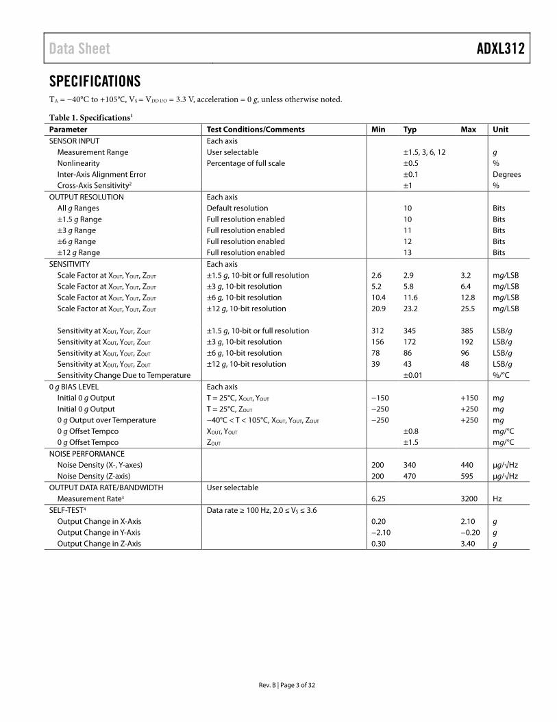
SPECIFICATIONS TA = −40°C to +105°C, VS = VDD I/O = 3.3 V, acceleration = 0 g, unless otherwise noted.
Table 1. Specifications1 Parameter Test Conditions/Comments Min Typ Max Unit SENSOR INPUT Each axis
Measurement Range User selectable ±1.5, 3, 6, 12 g Nonlinearity Percentage of full scale ±0.5 % Inter-Axis Alignment Error ±0.1 Degrees Cross-Axis Sensitivity2 ±1 %
OUTPUT RESOLUTION Each axis All g Ranges Default resolution 10 Bits ±1.5 g Range Full resolution enabled 10 Bits ±3 g Range Full resolution enabled 11 Bits ±6 g Range Full resolution enabled 12 Bits ±12 g Range Full resolution enabled 13 Bits
SENSITIVITY Each axis Scale Factor at XOUT, YOUT, ZOUT ±1.5 g, 10-bit or full resolution 2.6 2.9 3.2 mg/LSB Scale Factor at XOUT, YOUT, ZOUT ±3 g, 10-bit resolution 5.2 5.8 6.4 mg/LSB Scale Factor at XOUT, YOUT, ZOUT ±6 g, 10-bit resolution 10.4 11.6 12.8 mg/LSB Scale Factor at XOUT, YOUT, ZOUT ±12 g, 10-bit resolution 20.9 23.2 25.5 mg/LSB Sensitivity at XOUT, YOUT, ZOUT ±1.5 g, 10-bit or full resolution 312 345 385 LSB/g Sensitivity at XOUT, YOUT, ZOUT ±3 g, 10-bit resolution 156 172 192 LSB/g Sensitivity at XOUT, YOUT, ZOUT ±6 g, 10-bit resolution 78 86 96 LSB/g Sensitivity at XOUT, YOUT, ZOUT ±12 g, 10-bit resolution 39 43 48 LSB/g Sensitivity Change Due to Temperature ±0.01 %/°C
0 g BIAS LEVEL Each axis Initial 0 g Output T = 25°C, XOUT, YOUT −150 +150 mg Initial 0 g Output T = 25°C, ZOUT −250 +250 mg 0 g Output over Temperature −40°C < T < 105°C, XOUT, YOUT, ZOUT −250 +250 mg 0 g Offset Tempco XOUT, YOUT ±0.8 mg/°C 0 g Offset Tempco ZOUT ±1.5 mg/°C
NOISE PERFORMANCE Noise Density (X-, Y-axes) 200 340 440 µg/√Hz Noise Density (Z-axis) 200 470 595 µg/√Hz
OUTPUT DATA RATE/BANDWIDTH User selectable Measurement Rate3 6.25 3200 Hz
SELF-TEST4 Data rate ≥ 100 Hz, 2.0 ≤ VS ≤ 3.6 Output Change in X-Axis 0.20 2.10 g Output Change in Y-Axis −2.10 −0.20 g Output Change in Z-Axis 0.30 3.40 g
ADXL312 Data Sheet
Rev. B | Page 4 of 32
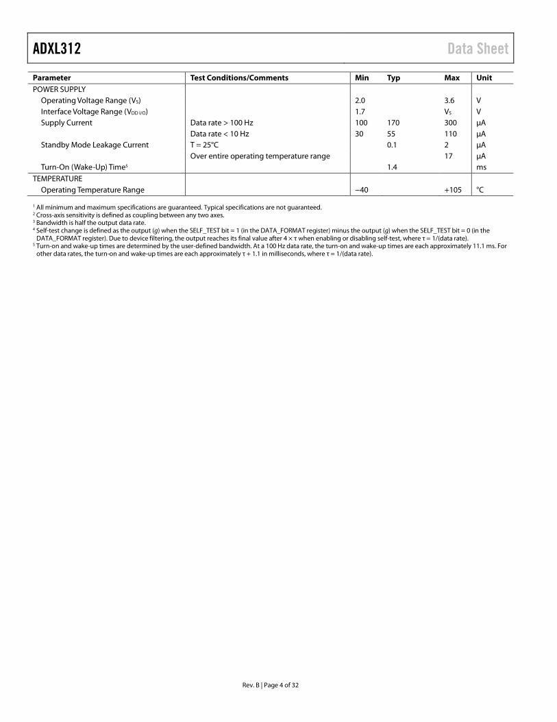
Parameter Test Conditions/Comments Min Typ Max Unit POWER SUPPLY
Operating Voltage Range (VS) 2.0 3.6 V Interface Voltage Range (VDD I/O) 1.7 VS V Supply Current Data rate > 100 Hz 100 170 300 µA Data rate < 10 Hz 30 55 110 µA Standby Mode Leakage Current T = 25°C 0.1 2 µA Over entire operating temperature range 17 µA Turn-On (Wake-Up) Time5 1.4 ms
TEMPERATURE Operating Temperature Range −40 +105 °C
1 All minimum and maximum specifications are guaranteed. Typical specifications are not guaranteed. 2 Cross-axis sensitivity is defined as coupling between any two axes. 3 Bandwidth is half the output data rate. 4 Self-test change is defined as the output (g) when the SELF_TEST bit = 1 (in the DATA_FORMAT register) minus the output (g) when the SELF_TEST bit = 0 (in the
DATA_FORMAT register). Due to device filtering, the output reaches its final value after 4 × τ when enabling or disabling self-test, where τ = 1/(data rate). 5 Turn-on and wake-up times are determined by the user-defined bandwidth. At a 100 Hz data rate, the turn-on and wake-up times are each approximately 11.1 ms. For
other data rates, the turn-on and wake-up times are each approximately τ + 1.1 in milliseconds, where τ = 1/(data rate).

Data Sheet ADXL312
Rev. B | Page 5 of 32
ABSOLUTE MAXIMUM RATINGS Table 2. Parameter Rating Acceleration
Any Axis, Unpowered 10,000 g Any Axis, Powered 10,000 g
VS −0.3 V to 3.9 V VDD I/O −0.3 V to 3.9 V All Other Pins −0.3 V to VDD I/O + 0.3 V or
3.9 V, whichever is less Output Short-Circuit Duration
(Any Pin to Ground) Indefinite
Temperature Range Powered −40°C to +125°C Storage −40°C to +125°C
Stresses at or above those listed under Absolute Maximum Ratings may cause permanent damage to the product. This is a stress rating only; functional operation of the product at these or any other conditions above those indicated in the operational section of this specification is not implied. Operation beyond the maximum operating conditions for extended periods may affect product reliability.
THERMAL RESISTANCE θJA is specified for the worst-case conditions, that is, a device soldered in a circuit board for surface-mount packages.
Table 3. Thermal Resistance Package Type θJA θJC Unit 32-Lead LFCSP Package 27.27 30 °C/W
ESD CAUTION

ADXL312 Data Sheet
Rev. B | Page 6 of 32
PIN CONFIGURATION AND FUNCTION DESCRIPTIONS
NOTES1. NC = NO CONNECT. DO NOT CONNECT TO THIS PIN.2. THE EXPOSED PAD MUST BE SOLDERED TO THE GROUND PLANE.
24 SDA/SDI/SDIO23 SPO/ALT ADDRESS22 RESERVED21 INT220 INT119 NC18 NC17 NC
12345678
GNDRESERVED
GNDGND
VSCS
RESERVEDNC
9 10 11 12 13 14 15 16
NC
NC
NC
NC
NC
NC
NC
NC
32 31 30 29 28 27 26 25
NC
V DD
I/ON
CN
CN
CN
CSC
L/SC
L KN
C
TOP VIEW(Not to Scale)
ADXL312
0879
1-00
2
Figure 2. Pin Configuration (Top View)
Table 4. Pin Function Descriptions Pin No. Mnemonic Description 1 GND This pin must be connected to ground. 2 Reserved Reserved. This pin must be connected to VS or left open. 3 GND This pin must be connected to ground. 4 GND This pin must be connected to ground. 5 VS Supply Voltage. 6 CS Chip Select.
7 Reserved Reserved. This pin must be left open. 8 to19 NC No Connect. Do not connect to this pin. 20 INT1 Interrupt 1 Output. 21 INT2 Interrupt 2 Output. 22 Reserved Reserved. This pin must be connected to GND. 23 SDO/ALT ADDRESS Serial Data Out, Alternate I2C Address Select. 24 SDA/SDI/SDIO Serial Data (I2C), Serial Data In (SPI 4-Wire), Serial Data In/Out (SPI 3-Wire). 25 NC No Connect. Do not connect to this pin. 26 SCL/SCLK Serial Communications Clock. 27 to 30 NC No Connect. Do not connect to this pin. 31 VDD I/O Digital Interface Supply Voltage. 32 NC No Connect. EP The exposed pad must be soldered to the ground plane.
Data Sheet ADXL312
Rev. B | Page 7 of 32
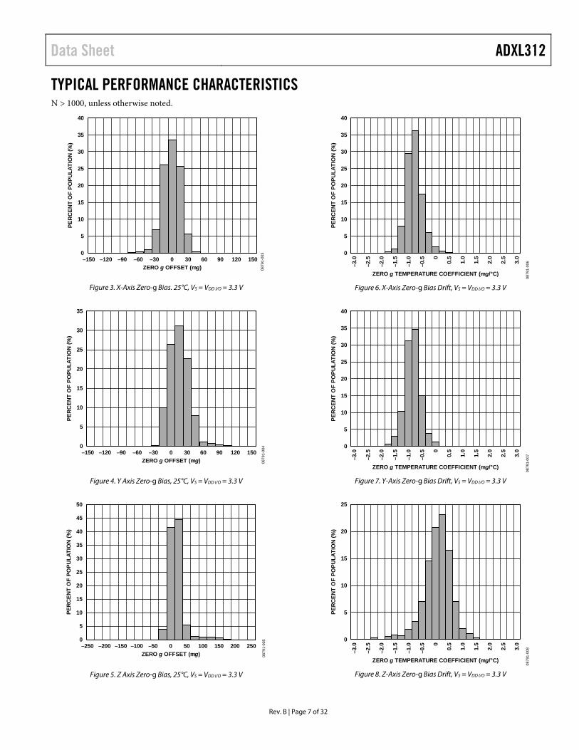
TYPICAL PERFORMANCE CHARACTERISTICS N > 1000, unless otherwise noted.
0
5
10
15
20
25
30
35
40
–150 –120 –60 –30–90 0 6030 90 120 150ZERO g OFFSET (mg)
PER
CEN
T O
F PO
PULA
TIO
N (%
)
0879
1-00
3
Figure 3. X-Axis Zero-g Bias. 25°C, VS = VDD I/O = 3.3 V
0
5
10
15
20
25
30
35
–150 –120 –60 –30–90 0 6030 90 120 150ZERO g OFFSET (mg)
PER
CEN
T O
F PO
PULA
TIO
N (%
)
0879
1-00
4
Figure 4. Y Axis Zero-g Bias, 25°C, VS = VDD I/O = 3.3 V
0
5
10
15
20
25
30
35
40
45
50
–250 –200 –100 –50–150 0 10050 150 200 250ZERO g OFFSET (mg)
PER
CEN
T O
F PO
PULA
TIO
N (%
)
0879
1-00
5
Figure 5. Z Axis Zero-g Bias, 25°C, VS = VDD I/O = 3.3 V
0
5
10
15
20
25
30
35
40
–3.0
–2.5
–2.0
–1.5
–1.0
–0.5 0
0.5
1.0
2.0
3.0
1.5
2.5
ZERO g TEMPERATURE COEFFICIENT (mg/°C)
PER
CEN
T O
F PO
PULA
TIO
N (%
)
0879
1-00
6
Figure 6. X-Axis Zero-g Bias Drift, VS = VDD I/O = 3.3 V
0
5
10
15
20
25
30
35
40
–3.0
–2.5
–2.0
–1.5
–1.0
–0.5 0
0.5
1.0
2.0
3.0
1.5
2.5
ZERO g TEMPERATURE COEFFICIENT (mg/°C)
PER
CEN
T O
F PO
PULA
TIO
N (%
)
0879
1-00
7
Figure 7. Y-Axis Zero-g Bias Drift, VS = VDD I/O = 3.3 V
0
5
10
15
20
25
–3.0
–2.5
–2.0
–1.5
–1.0
–0.5 0
0.5
1.0
2.0
3.0
1.5
2.5
ZERO g TEMPERATURE COEFFICIENT (mg/°C)
PER
CEN
T O
F PO
PULA
TIO
N (%
)
0879
1-00
8
Figure 8. Z-Axis Zero-g Bias Drift, VS = VDD I/O = 3.3 V

ADXL312 Data Sheet
Rev. B | Page 8 of 32
0
10
20
40
60
30
50
7031
2
318
324
330
336
342
348
354
360
372
384
366
378
SENSITIVITY (LSB/g)
PER
CEN
T O
F PO
PULA
TIO
N (%
)
0879
1-00
9
Figure 9. X-Axis Sensitivity, VS = VDD I/O = 3.3 V, 25°C
0
10
20
40
60
30
50
70
312
318
324
330
336
342
348
354
360
372
384
366
378
SENSITIVITY (LSB/g)
PER
CEN
T O
F PO
PULA
TIO
N (%
)
0879
1-01
0
Figure 10. Y-Axis Sensitivity, VS = VDD I/O = 3.3 V, 25°C
0
10
20
40
60
30
50
70
312
318
324
330
336
342
348
354
360
372
384
366
378
SENSITIVITY (LSB/g)
PER
CEN
T O
F PO
PULA
TIO
N (%
)
0879
1-01
1
Figure 11. Z-Axis Sensitivity, VS = VDD I/O = 3.3 V, 25°C
0
5
10
20
15
25
30
–0.0
30
–0.0
25
–0.0
20
–0.0
15
–0.0
10
–0.0
05 0
0.00
5
0.01
0
0.02
0
0.03
0
0.01
5
0.02
5
SENSITIVITY TEMPERATURE COEFFICIENT (%/°C)
PER
CEN
T O
F PO
PULA
TIO
N (%
)
0879
1-01
2
Figure 12. X-Axis Sensitivity Temperature Coefficient, VS = VDD I/O = 3.3 V
0
5
10
20
15
25
35
30
–0.0
30
–0.0
25
–0.0
20
–0.0
15
–0.0
10
–0.0
05 0
0.00
5
0.01
0
0.02
0
0.03
0
0.01
5
0.02
5
SENSITIVITY TEMPERATURE COEFFICIENT (%/°C)
PER
CEN
T O
F PO
PULA
TIO
N (%
)
0879
1-01
3
Figure 13. Y-Axis Sensitivity Temperature Coefficient, VS = VDD I/O = 3.3 V
0
5
10
20
15
25
35
30
–0.0
30
–0.0
25
–0.0
20
–0.0
15
–0.0
10
–0.0
05 0
0.00
5
0.01
0
0.02
0
0.03
0
0.01
5
0.02
5
SENSITIVITY TEMPERATURE COEFFICIENT (%/°C)
PER
CEN
T O
F PO
PULA
TIO
N (%
)
0879
1-01
4
Figure 14. Z-Axis Sensitivity Temperature Coefficient, VS = VDD I/O = 3.3 V

Data Sheet ADXL312
Rev. B | Page 9 of 32
0
10
20
40
30
50
80
70
60
0.2 0.4 0.6 0.8 1.0 1.2 1.4 1.6 1.8 2.0SELF-TEST RESPONSE (g)
PER
CEN
T O
F PO
PULA
TIO
N (%
)
0879
1-01
5
Figure 15. X-Axis Self-Test Delta, VS = VDD I/O = 3.3 V, 25°C
0
10
20
40
30
50
70
60
–2.1
–1.9
–1.7
–1.5
–1.3
–1.1
–0.9
–0.7
–0.5
–0.3
SELF-TEST RESPONSE (g)
PER
CEN
T O
F PO
PULA
TIO
N (%
)
0879
1-01
6
Figure 16. Y-Axis Self-Test Delta, VS = VDD I/O = 3.3 V, 25°C
0
10
20
40
30
50
80
70
60
0.3 0.6 0.9 1.2 1.5 1.8 2.1 2.4 2.7 3.33.0
SELF-TEST RESPONSE (g)
PER
CEN
T O
F PO
PULA
TIO
N (%
)
0879
1-01
7
Figure 17. Z-Axis Self-Test Delta, VS = VDD I/O = 3.3 V, 25°C
0
10
20
40
30
50
80
70
60
30 50 70 90 110
130
150
170
190
210
230
250
270
290
310
CURRENT (nA)
PER
CEN
T O
F PO
PULA
TIO
N (%
)
0879
1-01
8
Figure 18. Standby Mode Current Consumption, VS = VDD I/O = 3.3 V, 25°C
0
5
10
20
15
25
35
30
100
120
140
160
180
200
220
240
260
280
300
CURRENT CONSUMPTION (µA)
PER
CEN
T O
F PO
PULA
TIO
N (%
)
0879
1-01
9
Figure 19. Current Consumption, Measurement Mode, Data Rate = 100 Hz, VS = VDD I/O = 3.3 V, 25°C
0
50
100
150
200
2.0 2.4 2.8 3.2 3.6
SUPPLY VOLTAGE (V)
SUPP
LY C
UR
REN
T (µ
A)
0879
1-23
3
Figure 20. Supply Current vs. Supply Voltage, VS at 25°C

ADXL312 Data Sheet
Rev. B | Page 10 of 32
THEORY OF OPERATION The ADXL312 is a complete 3-axis acceleration measurement system with a selectable measurement range of ±1.5 g, ±3 g, ±6 g, or ±12 g. It measures both dynamic acceleration resulting from motion or shock and static acceleration, such as gravity, which allows it to be used as a tilt sensor.
The sensor is a polysilicon surface-micromachined structure built on top of a silicon wafer. Polysilicon springs suspend the structure over the surface of the wafer and provide a resistance against acceleration forces.
Deflection of the structure is measured using differential capacitors that consist of independent fixed plates and plates attached to the moving mass. Acceleration deflects the beam and unbalances the differential capacitor, resulting in a sensor output whose amplitude is proportional to acceleration. Phase-sensitive demodulation is used to determine the magnitude and polarity of the acceleration.
POWER SEQUENCING Power can be applied to VS or VDD I/O in any sequence without damaging the ADXL312. All possible power-on modes are summarized in Table 5. The interface voltage level is set with the interface supply voltage, VDD I/O, which must be present to ensure that the ADXL312 does not create a conflict on the communication bus. For single-supply operation, VDD I/O can be the same as the main supply, VS. In a dual-supply application, however, VDD I/O can differ from VS to accommodate the desired interface voltage, as long as VS is greater than or equal to VDD I/O.
After VS is applied, the device enters standby mode, where power consumption is minimized and the device waits for VDD I/O to be applied and for the command to enter measurement mode to be received. (This command can be initiated by setting the measure bit in the POWER_CTL register (Address 0x2D).) In addition, any register can be written to or read from to configure the part while the device is in standby mode. It is recommended to configure the device in standby mode and then to enable measurement mode. Clearing the measure bit returns the device to the standby mode.
Table 5. Power Sequencing Condition VS VDD I/O Description Power Off Off Off The device is completely off, but
there is a potential for a communication bus conflict.
Bus Disabled On Off The device is on in standby mode, but communication is unavailable and creates a conflict on the communication bus. The duration of this state must be minimized during power-up to prevent a conflict.
Bus Enabled Off On No functions are available, but the device will not create a conflict on the communication bus.
Standby or Measurement
On On The device is in standby mode, awaiting a command to enter measurement mode, and all sensor functions are off. After the device is instructed to enter measurement mode, all sensor functions are available.
POWER SAVINGS Power Modes
The ADXL312 automatically modulates its power consumption in proportion to its output data rate, as outlined in Table 6. If additional power savings is desired, a lower power mode is available. In this mode, the internal sampling rate is reduced, allowing for power savings in the 12.5 Hz to 400 Hz data rate range at the expense of slightly greater noise. To enter low power mode, set the LOW_POWER bit (Bit 4) in the BW_RATE register (Address 0x2C). The current consumption in low power mode is shown in Table 7 for cases where there is an advantage to using low power mode. Use of low power mode for a data rate not shown in Table 7 does not provide any advantage over the same data rate in normal power mode. Therefore, it is recommended that only data rates shown in Table 7 be used in low power mode. The current consumption values shown in Table 6 and Table 7 are for a VS of 3.3 V.

Data Sheet ADXL312
Rev. B | Page 11 of 32
Table 6. Current Consumption vs. Data Rate (TA = 25°C, VS = VDD I/O = 3.3 V) Output Data Rate (Hz) Bandwidth (Hz) Rate Code IDD (µA) 3200 1600 1111 170 1600 800 1110 115 800 400 1101 170 400 200 1100 170 200 100 1011 170 100 50 1010 170 50 25 1001 115 25 12.5 1000 82 12.5 6.25 0111 65 6.25 3.125 0110 57
Table 7. Current Draw vs. Data Rate, Low Power Mode (TA = 25°C, VS = VDD I/O = 3.3 V) Output Data Rate (Hz) Bandwidth (Hz) Rate Code IDD (µA) 400 200 1100 115 200 100 1011 82 100 50 1010 65 50 25 1001 57 25 12.5 1000 50 12.5 6.25 0111 43
Autosleep Mode
Additional power savings can be had by having the ADXL312 automatically switch to sleep mode during periods of inactivity. To enable this feature, set the THRESH_INACT register (Address 0x25) to an acceleration threshold value. Levels of acceleration below this threshold are regarded as no activity levels. Set TIME_INACT (Address 0x26) to an appropriate inactivity time period. Then set the AUTO_SLEEP bit and the link bit in the POWER_CTL register (Address 0x2D). If the device does not detect a level of acceleration in excess of THRES_INACT for TIME_INACT seconds, then the device is transitioned to sleep mode automatically. Current consumption at the sub-8 Hz data rates used in this mode is typically 30 µA for a VS of 3.3 V.
Standby Mode
For even lower power operation, standby mode can be used. In standby mode, current consumption is reduced to 0.1µA (typical). In this mode, no measurements are made. Standby mode is entered by clearing the measure bit (Bit 3) in the POWER_CTL register (Address 0x2D). Placing the device into standby mode preserves the contents of the FIFO.
ADXL312 Data Sheet
Rev. B | Page 12 of 32
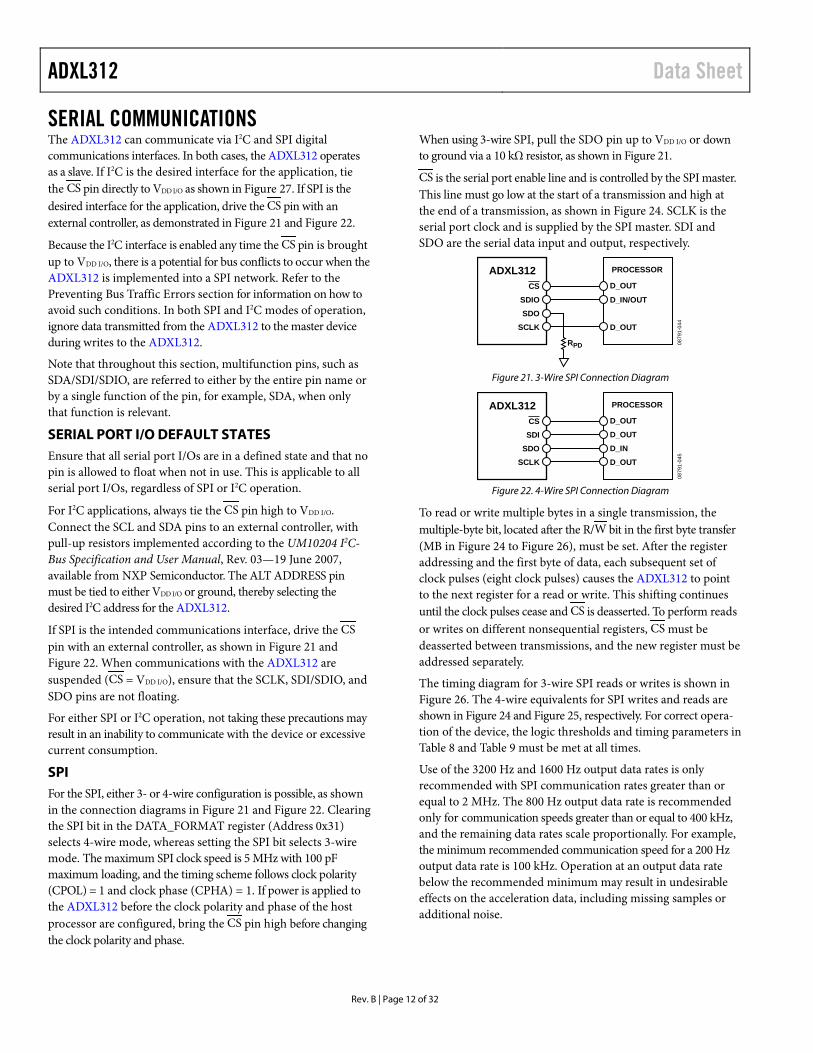
SERIAL COMMUNICATIONS The ADXL312 can communicate via I2C and SPI digital communications interfaces. In both cases, the ADXL312 operates as a slave. If I2C is the desired interface for the application, tie the CS pin directly to VDD I/O as shown in Figure 27. If SPI is the desired interface for the application, drive the CS pin with an external controller, as demonstrated in Figure 21 and Figure 22.
Because the I2C interface is enabled any time the CS pin is brought up to VDD I/O, there is a potential for bus conflicts to occur when the ADXL312 is implemented into a SPI network. Refer to the Preventing Bus Traffic Errors section for information on how to avoid such conditions. In both SPI and I2C modes of operation, ignore data transmitted from the ADXL312 to the master device during writes to the ADXL312.
Note that throughout this section, multifunction pins, such as SDA/SDI/SDIO, are referred to either by the entire pin name or by a single function of the pin, for example, SDA, when only that function is relevant.
SERIAL PORT I/O DEFAULT STATES Ensure that all serial port I/Os are in a defined state and that no pin is allowed to float when not in use. This is applicable to all serial port I/Os, regardless of SPI or I2C operation.
For I2C applications, always tie the CS pin high to VDD I/O. Connect the SCL and SDA pins to an external controller, with pull-up resistors implemented according to the UM10204 I2C-Bus Specification and User Manual, Rev. 03—19 June 2007, available from NXP Semiconductor. The ALT ADDRESS pin must be tied to either VDD I/O or ground, thereby selecting the desired I2C address for the ADXL312.
If SPI is the intended communications interface, drive the CS pin with an external controller, as shown in Figure 21 and Figure 22. When communications with the ADXL312 are suspended (CS = VDD I/O), ensure that the SCLK, SDI/SDIO, and SDO pins are not floating.
For either SPI or I2C operation, not taking these precautions may result in an inability to communicate with the device or excessive current consumption.
SPI For the SPI, either 3- or 4-wire configuration is possible, as shown in the connection diagrams in Figure 21 and Figure 22. Clearing the SPI bit in the DATA_FORMAT register (Address 0x31) selects 4-wire mode, whereas setting the SPI bit selects 3-wire mode. The maximum SPI clock speed is 5 MHz with 100 pF maximum loading, and the timing scheme follows clock polarity (CPOL) = 1 and clock phase (CPHA) = 1. If power is applied to the ADXL312 before the clock polarity and phase of the host processor are configured, bring the CS pin high before changing the clock polarity and phase.
When using 3-wire SPI, pull the SDO pin up to VDD I/O or down to ground via a 10 kΩ resistor, as shown in Figure 21.
CS is the serial port enable line and is controlled by the SPI master. This line must go low at the start of a transmission and high at the end of a transmission, as shown in Figure 24. SCLK is the serial port clock and is supplied by the SPI master. SDI and SDO are the serial data input and output, respectively.
0879
1-04
4
ADXL312 PROCESSOR
CSSDIOSDO
SCLK
D_OUT
D_IN/OUT
D_OUT
RPD
Figure 21. 3-Wire SPI Connection Diagram
0879
1-04
5
ADXL312 PROCESSOR
CSSDI
SDOSCLK
D_OUT
D_OUT
D_IN
D_OUT
Figure 22. 4-Wire SPI Connection Diagram
To read or write multiple bytes in a single transmission, the multiple-byte bit, located after the R/W bit in the first byte transfer (MB in Figure 24 to Figure 26), must be set. After the register addressing and the first byte of data, each subsequent set of clock pulses (eight clock pulses) causes the ADXL312 to point to the next register for a read or write. This shifting continues until the clock pulses cease and CS is deasserted. To perform reads or writes on different nonsequential registers, CS must be deasserted between transmissions, and the new register must be addressed separately.
The timing diagram for 3-wire SPI reads or writes is shown in Figure 26. The 4-wire equivalents for SPI writes and reads are shown in Figure 24 and Figure 25, respectively. For correct opera-tion of the device, the logic thresholds and timing parameters in Table 8 and Table 9 must be met at all times.
Use of the 3200 Hz and 1600 Hz output data rates is only recommended with SPI communication rates greater than or equal to 2 MHz. The 800 Hz output data rate is recommended only for communication speeds greater than or equal to 400 kHz, and the remaining data rates scale proportionally. For example, the minimum recommended communication speed for a 200 Hz output data rate is 100 kHz. Operation at an output data rate below the recommended minimum may result in undesirable effects on the acceleration data, including missing samples or additional noise.

Data Sheet ADXL312
Rev. B | Page 13 of 32
Preventing Bus Traffic Errors
The ADXL312 CS pin initiates SPI transactions and enables I2C mode. When the ADXL312 is used on a SPI bus with multiple devices, its CS pin is held high while the master communicates with the other devices. There may be conditions where a SPI command transmitted to another device looks like a valid I2C command. In this case, the ADXL312 interprets this as an attempt to communicate in I2C mode and may interfere with other bus traffic. Unless bus traffic can be adequately controlled to ensure such a condition never occurs, it is recommended to add a logic gate in front of the SDI pin, as shown in Figure 23.
This OR gate holds the SDA line high when CS is high to prevent bus traffic at the ADXL312 from appearing as an I2C start command.
0879
1-04
6
ADXL312 PROCESSOR
CS
SDI
SDOSCLK
D_OUT
D_OUT
D_IN
D_OUT
Figure 23. Recommended SPI Connection Diagram when Using Multiple SPI Devices on a Single Bus
Table 8. SPI Digital Input/Output Limit1 Parameter Test Conditions Min Max Unit Digital Input
Low Level Input Voltage (VIL) 0.3 × VDD I/O V High Level Input Voltage (VIH) 0.7 × VDD I/O V Low Level Input Current (IIL) VIN = VDD I/O 0.1 µA High Level Input Current (IIH) VIN = 0 V −0.1 µA
Digital Output Low Level Output Voltage (VOL) IOL = 10 mA 0.2 × VDD I/O V High Level Output Voltage (VOH) IOH = −4 mA 0.8 × VDD I/O V Low Level Output Current (IOL) VOL = VOL, max 10 mA High Level Output Current (IOH) VOH = VOH, min −4 mA
Pin Capacitance fIN = 1 MHz, VIN = 2.5 V 8 pF 1 Limits based on characterization results, not production tested.
Table 9. SPI Timing (TA = 25°C, VS = VDD I/O = 3.3 V)1 Limit2, 3 Parameter Min Max Unit Description fSCLK 5 MHz SPI clock frequency. tSCLK 200 ns 1/(SPI clock frequency) mark-space ratio for the SCLK input is 40/60 to 60/40. tDELAY 5 ns CS falling edge to SCLK falling edge .
tQUIET 5 ns SCLK rising edge to CS rising edge.
tDIS 10 ns CS rising edge to SDO disabled.
tCS,DIS 150 ns CS deassertion between SPI communications.
tS 0.3 × tSCLK ns SCLK low pulse width (space). tM 0.3 × tSCLK ns SCLK high pulse width (mark). tSETUP 5 ns SDI valid before SCLK rising edge. tHOLD 5 ns SDI valid after SCLK rising edge. tSDO 40 ns SCLK falling edge to SDO/SDIO output transition. tR
4 20 ns SDO/SDIO output high to output low transition. tF
4 20 ns SDO/SDIO output low to output high transition. 1 The CS, SCLK, SDI, and SDO pins are not internally pulled up or down; they must be driven for proper operation. 2 Limits based on characterization results, characterized with fSCLK = 5 MHz and bus load capacitance of 100 pF; not production tested. 3 The timing values are measured corresponding to the input thresholds (VIL and VIH) given in Table 8. 4 Output rise and fall times measured with capacitive load of 150 pF.

ADXL312 Data Sheet
Rev. B | Page 14 of 32
tDELAY
tSETUP tHOLD
tSDO
tR, tF
X X X
W MB A5 A0 D7 D0
X X X
ADDRESS BITS DATA BITS
tSCLK tM tS tQUIET
tDIS
tCS,DIS
SCLK
SDI
SDO
CS
0879
1-12
9
Figure 24. SPI 4-Wire Write
CS
X X X
R MB A5 A0
D7 D0X
X X
ADDRESS BITS
DATA BITS
tDIS
SCLK
SDI
SDO
tQUIET
tSDO
tSETUP
tDELAYtSCLK tM tS
tR, tF
tHOLD
tCS,DIS
0879
1-13
0
Figure 25. SPI 4-Wire Read
CS
tDELAY
tSETUP tHOLD tSDO
R/W MB A5 A0 D7 D0
ADDRESS BITS DATA BITS
tSCLK tM tS tQUIET
SCLK
SDIO
SDO
NOTES1. tSDO IS ONLY PRESENT DURING READS.
tR, tF
tCS,DIS
0879
1-13
1
Figure 26. SPI 3-Wire Read/Write
Data Sheet ADXL312
Rev. B | Page 15 of 32
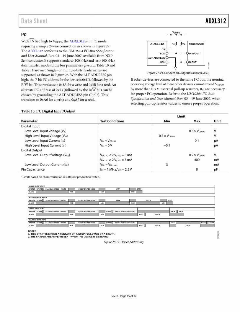
I2C
With CS tied high to VDD I/O, the ADXL312 is in I2C mode, requiring a simple 2-wire connection as shown in Figure 27. The ADXL312 conforms to the UM10204 I2C-Bus Specification and User Manual, Rev. 03—19 June 2007, available from NXP Semiconductor. It supports standard (100 kHz) and fast (400 kHz) data transfer modes if the bus parameters given in Table 10 and Table 11 are met. Single- or multiple-byte reads/writes are supported, as shown in Figure 28. With the ALT ADDRESS pin high, the 7-bit I2C address for the device is 0x1D, followed by the R/W bit. This translates to 0x3A for a write and 0x3B for a read. An alternate I2C address of 0x53 (followed by the R/W bit) can be chosen by grounding the ALT ADDRESS pin (Pin 7). This translates to 0xA6 for a write and 0xA7 for a read.
PROCESSOR
D IN/OUT
D OUT
RP
VDD I/O
RPADXL312CS
SDA
ALT ADDRESS
SCL
0879
1-03
2
Figure 27. I2C Connection Diagram (Address 0x53)
If other devices are connected to the same I2C bus, the nominal operating voltage level of these other devices cannot exceed VDD I/O by more than 0.3 V. External pull-up resistors, RP, are necessary for proper I2C operation. Refer to the UM10204 I2C-Bus Specification and User Manual, Rev. 03—19 June 2007, when selecting pull-up resistor values to ensure proper operation.
Table 10. I2C Digital Input/Output Limit1 Parameter Test Conditions Min Max Unit Digital Input
Low Level Input Voltage (VIL) 0.3 × VDD I/O V High Level Input Voltage (VIH) 0.7 × VDD I/O V Low Level Input Current (IIL) VIN = VDD I/O 0.1 µA High Level Input Current (IIH) VIN = 0 V −0.1 µA
Digital Output Low Level Output Voltage (VOL) VDD I/O < 2 V, IOL = 3 mA 0.2 × VDD I/O V VDD I/O ≥ 2 V, IOL = 3 mA 400 mV Low Level Output Current (IOL) VOL = VOL, max 3 mA
Pin Capacitance fIN = 1 MHz, VIN = 2.5 V 8 pF 1 Limits based on characterization results; not production tested.
NOTES1. THIS START IS EITHER A RESTART OR A STOP FOLLOWED BY A START.2. THE SHADED AREAS REPRESENT WHEN THE DEVICE IS LISTENING.
0879
1-03
3
MASTER START SLAVE ADDRESS + WRITE REGISTER ADDRESS
SLAVE ACK ACK ACK
MASTER START SLAVE ADDRESS + WRITE REGISTER ADDRESS
SLAVE ACK ACK ACK ACK
MASTER START SLAVE ADDRESS + WRITE REGISTER ADDRESS STOP
SLAVE ACK ACK
MASTER START
START1
START1SLAVE ADDRESS + WRITE REGISTER ADDRESS NACK STOP
SLAVE ACK ACK DATA
STOP
ACK
SINGLE-BYTE WRITE
MULTIPLE-BYTE WRITE
DATA
DATA
MULTIPLE-BYTE READ
SLAVE ADDRESS + READ
SLAVE ADDRESS + READACK
DATA
DATA
DATA
STOP
NACK
ACK
SINGLE-BYTE READ
Figure 28. I2C Device Addressing

ADXL312 Data Sheet
Rev. B | Page 16 of 32
Table 11. I2C Timing (TA = 25°C, VS = VDD I/O = 3.3 V) Limit1, 2 Parameter Min Max Unit Description fSCL 400 kHz SCL clock frequency t1 2.5 µs SCL cycle time t2 0.6 µs tHIGH, SCL high time t3 1.3 µs tLOW, SCL low time t4 0.6 µs tHD, STA, start/repeated start condition hold time t5 100 ns tSU, DAT, data setup time t6
3, 4, 5, 6 0 0.9 µs tHD, DAT, data hold time t7 0.6 µs tSU, STA, setup time for repeated start t8 0.6 µs tSU, STO, stop condition setup time t9 1.3 µs tBUF, bus-free time between a stop condition and a start condition t10 300 ns tR, rise time of both SCL and SDA when receiving 0 ns tR, rise time of both SCL and SDA when receiving or transmitting t11 250 ns tF, fall time of SDA when receiving 300 ns tF, fall time of both SCL and SDA when transmitting 20 + 0.1 Cb
7 ns tF, fall time of both SCL and SDA when transmitting or receiving Cb 400 pF Capacitive load for each bus line 1 Limits based on characterization results, with fSCL = 400 kHz and a 3 mA sink current; not production tested. 2 All values referred to the VIH and the VIL levels given in Table 10. 3 t6 is the data hold time that is measured from the falling edge of SCL. It applies to data in transmission and acknowledge. 4 A transmitting device must internally provide an output hold time of at least 300 ns for the SDA signal (with respect to VIH(min) of the SCL signal) to bridge the
undefined region of the falling edge of SCL. 5 The maximum t6 value must be met only if the device does not stretch the low period (t3) of the SCL signal. 6 The maximum value for t6 is a function of the clock low time (t3), the clock rise time (t10), and the minimum data setup time (t5(min)). This value is calculated as
t6(max) = t3 − t10 − t5(min). 7 Cb is the total capacitance of one bus line in picofarads.
SDA
t9
SCL
t3 t10 t11t4
t4 t6 t2 t5 t7 t1 t8
STARTCONDITION
REPEATEDSTART
CONDITION
STOPCONDITION
0879
1-03
4
Figure 29. I2C Timing Diagram

Data Sheet ADXL312
Rev. B | Page 17 of 32
INTERRUPTS The ADXL312 provides two output pins for driving interrupts: INT1 and INT2. Both interrupt pins are push-pull, low impedance pins with output specifications shown in Table 12. The default configuration of the interrupt pins is active high. This can be changed to active low by setting the INT_INVERT bit in the DATA_FORMAT (Address 0x31) register. All functions can be used simultaneously, with the only limiting feature being that some functions may need to share interrupt pins.
Interrupts are enabled by setting the appropriate bit in the INT_ENABLE register (Address 0x2E) and are mapped to either the INT1 or INT2 pin based on the contents of the INT_MAP register (Address 0x2F). When initially configuring the interrupt pins, it is recommended that the functions and interrupt mapping be done before enabling the interrupts. When changing the con-figuration of an interrupt, it is recommended that the interrupt be disabled first, by clearing the bit corresponding to that function in the INT_ENABLE register, and then the function be reconfigured before enabling the interrupt again. Configuration of the functions while the interrupts are disabled helps to prevent the accidental generation of an interrupt before desired.
The interrupt functions are latched and cleared by either reading the data registers (Address 0x32 to Address 0x37) until the inter-rupt condition is no longer valid for the data-related interrupts or by reading the INT_SOURCE register (Address 0x30) for the remaining interrupts. This section describes the interrupts that can be set in the INT_ENABLE register and monitored in the INT_SOURCE register.
DATA_READY
The DATA_READY bit is set when new data is available and is cleared when no new data is available.
Activity
The activity bit is set when acceleration greater than the value stored in the THRESH_ACT register (Address 0x24) is experienced.
Inactivity
The inactivity bit is set when acceleration of less than the value stored in the THRESH_INACT register (Address 0x25) is experienced for more time than is specified in the TIME_INACT register (Address 0x26). The maximum value for TIME_INACT is 255 sec.
Watermark
The watermark bit is set when the number of samples in FIFO equals the value stored in the samples bits (Register FIFO_CTL, Address 0x38). The watermark bit is cleared automatically when FIFO is read, and the content returns to a value below the value stored in the samples bits.
Overrun
The overrun bit is set when new data replaces unread data. The precise operation of the overrun function depends on the FIFO mode. In bypass mode, the overrun bit is set when new data replaces unread data in the DATAX, DATAY, and DATAZ registers (Address 0x32 to Address 0x37). In all other modes, the overrun bit is set when FIFO is filled. The overrun bit is automatically cleared when the contents of FIFO are read.
Table 12. Interrupt Pin Digital Output Limit1 Parameter Test Conditions Min Max Unit Digital Output
Low Level Output Voltage (VOL) IOL = 300 µA 0.2 × VDD I/O V High Level Output Voltage (VOH) IOH = −150 µA 0.8 × VDD I/O V Low Level Output Current (IOL) VOL = VOL, max 300 µA High Level Output Current (IOH) VOH = VOH, min −150 µA
Pin Capacitance fIN = 1 MHz, VIN = 2.5 V 8 pF Rise/Fall Time
Rise Time (tR)2 CLOAD = 150 pF 210 ns Fall Time (tF)3 CLOAD = 150 pF 150 ns
1 Limits based on characterization results, not production tested. 2 Rise time is measured as the transition time from VOL, max to VOH, min of the interrupt pin. 3 Fall time is measured as the transition time from VOH, min to VOL, max of the interrupt pin.

ADXL312 Data Sheet
Rev. B | Page 18 of 32
FIFO The ADXL312 contains technology for an embedded memory management system with 32-level FIFO that can be used to minimize host processor burden. This buffer has four modes: bypass, FIFO, stream, and trigger (see Table 21). Each mode is selected by the settings of the FIFO_MODE bits in the FIFO_CTL register (Address 0x38).
Bypass Mode
In bypass mode, FIFO is not operational and, therefore, remains empty.
FIFO Mode
In FIFO mode, data from measurements of the x-, y-, and z-axes are stored in FIFO. When the number of samples in FIFO equals the level specified in the samples bits of the FIFO_CTL register (Address 0x38), the watermark interrupt is set. FIFO continues accumulating samples until it is full (32 samples from measurements of the x-, y-, and z-axes) and then stops collecting data. After FIFO stops collecting data, the device continues to operate; therefore, features such as activity detection can be used after FIFO is full. The watermark interrupt continues to occur until the number of samples in FIFO is less than the value stored in the samples bits of the FIFO_CTL register.
Stream Mode
In stream mode, data from measurements of the x-, y-, and z-axes are stored in FIFO. When the number of samples in FIFO equals the level specified in the samples bits of the FIFO_CTL register (Address 0x38), the watermark interrupt is set. FIFO continues accumulating samples and holds the latest 32 samples from measurements of the x-, y-, and z-axes, discarding older data as new data arrives. The watermark interrupt continues occurring until the number of samples in FIFO is less than the value stored in the samples bits of the FIFO_CTL register.
Trigger Mode
In trigger mode, FIFO accumulates samples, holding the latest 32 samples from measurements of the x-, y-, and z-axes. After a trigger event occurs and an interrupt is sent to the INT1 or INT2 pin (determined by the trigger bit in the FIFO_CTL register),
FIFO keeps the last n samples (where n is the value specified by the samples bits in the FIFO_CTL register) and then operates in FIFO mode, collecting new samples only when FIFO is not full. A delay of at least 5 μs must be present between the trigger event occurring and the start of reading data from the FIFO to allow the FIFO to discard and retain the necessary samples. Additional trigger events cannot be recognized until the trigger mode is reset. To reset the trigger mode, set the device to bypass mode and then set the device back to trigger mode. Note that the FIFO data must be read first because placing the device into bypass mode clears FIFO.
Retrieving Data from FIFO
The FIFO data is read through the DATAX, DATAY, and DATAZ registers (Address 0x32 to Address 0x37). When the FIFO is in FIFO, stream, or trigger mode, reads to the DATAX, DATAY, and DATAZ registers read data stored in the FIFO. Each time data is read from the FIFO, the oldest x-, y-, and z-axes data is placed into the DATAX, DATAY and DATAZ registers.
If a single-byte read operation is performed, the remaining bytes of data for the current FIFO sample are lost. Therefore, all axes of interest must be read in a burst (or multiple-byte) read operation. To ensure that the FIFO has completely popped (that is, that new data has completely moved into the DATAX, DATAY, and DATAZ registers), there must be at least 5 μs between the end of reading the data registers and the start of a new read of the FIFO or a read of the FIFO_STATUS register (Address 0x39). The end of reading a data register is signified by the transition from Register 0x37 to Register 0x38 or by the CS pin going high.
For SPI operation at 1.6 MHz or less, the register addressing portion of the transmission is a sufficient delay to ensure that the FIFO has completely popped. For SPI operation greater than 1.6 MHz, it is necessary to deassert the CS pin to ensure a total delay of 5 μs; otherwise, the delay will not be sufficient. The total delay necessary for 5 MHz operation is at most 3.4 μs. This is not a concern when using I2C mode because the communication rate is low enough to ensure a sufficient delay between FIFO reads.
Data Sheet ADXL312
Rev. B | Page 19 of 32
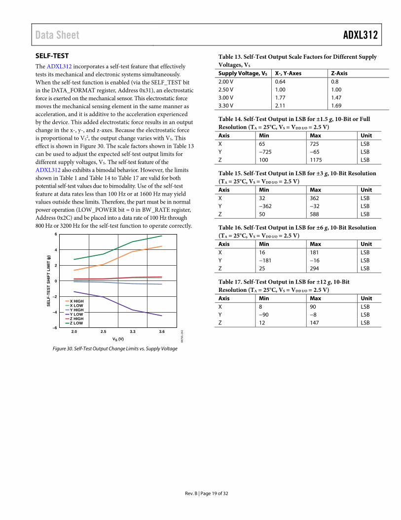
SELF-TEST The ADXL312 incorporates a self-test feature that effectively tests its mechanical and electronic systems simultaneously. When the self-test function is enabled (via the SELF_TEST bit in the DATA_FORMAT register, Address 0x31), an electrostatic force is exerted on the mechanical sensor. This electrostatic force moves the mechanical sensing element in the same manner as acceleration, and it is additive to the acceleration experienced by the device. This added electrostatic force results in an output change in the x-, y-, and z-axes. Because the electrostatic force is proportional to VS
2, the output change varies with VS. This effect is shown in Figure 30. The scale factors shown in Table 13 can be used to adjust the expected self-test output limits for different supply voltages, VS. The self-test feature of the ADXL312 also exhibits a bimodal behavior. However, the limits shown in Table 1 and Table 14 to Table 17 are valid for both potential self-test values due to bimodality. Use of the self-test feature at data rates less than 100 Hz or at 1600 Hz may yield values outside these limits. Therefore, the part must be in normal power operation (LOW_POWER bit = 0 in BW_RATE register, Address 0x2C) and be placed into a data rate of 100 Hz through 800 Hz or 3200 Hz for the self-test function to operate correctly.
–6
–4
–2
0
2
4
6
2.0 2.5 3.3 3.6
VS (V)
SELF
-TES
T SH
IFT
LIM
IT (g
)
X HIGHX LOWY HIGHY LOWZ HIGHZ LOW
0879
1-24
2
Figure 30. Self-Test Output Change Limits vs. Supply Voltage
Table 13. Self-Test Output Scale Factors for Different Supply Voltages, VS Supply Voltage, VS X-, Y-Axes Z-Axis 2.00 V 0.64 0.8 2.50 V 1.00 1.00 3.00 V 1.77 1.47 3.30 V 2.11 1.69
Table 14. Self-Test Output in LSB for ±1.5 g, 10-Bit or Full Resolution (TA = 25°C, VS = VDD I/O = 2.5 V) Axis Min Max Unit X 65 725 LSB Y −725 −65 LSB Z 100 1175 LSB
Table 15. Self-Test Output in LSB for ±3 g, 10-Bit Resolution (TA = 25°C, VS = VDD I/O = 2.5 V) Axis Min Max Unit X 32 362 LSB Y −362 −32 LSB Z 50 588 LSB
Table 16. Self-Test Output in LSB for ±6 g, 10-Bit Resolution (TA = 25°C, VS = VDD I/O = 2.5 V) Axis Min Max Unit X 16 181 LSB Y −181 −16 LSB Z 25 294 LSB
Table 17. Self-Test Output in LSB for ±12 g, 10-Bit Resolution (TA = 25°C, VS = VDD I/O = 2.5 V) Axis Min Max Unit X 8 90 LSB Y −90 −8 LSB Z 12 147 LSB

ADXL312 Data Sheet
Rev. B | Page 20 of 32
REGISTER MAP Table 18. Register Map
Address Hex Dec Name Type Reset Value Description 0x00 0 DEVID R 11100101 Device ID. 0x01 to 0x1D 1 to 29 Reserved Reserved. Do not access. 0x1E 30 OFSX R/W 00000000 X-axis offset.
0x1F 31 OFSY R/W 00000000 Y-axis offset.
0x20 32 OFSZ R/W 00000000 Z-axis offset.
0x21 33 Reserved Reserved. Do not access. 0x22 34 Reserved Reserved. Do not access. 0x23 35 Reserved Reserved. Do not access. 0x24 36 THRESH_ACT R/W 00000000 Activity threshold.
0x25 37 THRESH_INACT R/W 00000000 Inactivity threshold.
0x26 38 TIME_INACT R/W 00000000 Inactivity time.
0x27 39 ACT_INACT_CTL R/W 00000000 Axis enable control for activity and inactivity detection.
0x28 40 Reserved Reserved. Do not access. 0x29 41 Reserved Reserved. Do not access. 0x2A 42 Reserved Reserved. Do not access. 0x2B 43 Reserved Reserved. Do not access. 0x2C 44 BW_RATE R/W 00001010 Data rate and power mode control.
0x2D 45 POWER_CTL R/W 00000000 Power-saving features control.
0x2E 46 INT_ENABLE R/W 00000000 Interrupt enable control.
0x2F 47 INT_MAP R/W 00000000 Interrupt mapping control.
0x30 48 INT_SOURCE R 00000010 Source of interrupts. 0x31 49 DATA_FORMAT R/W 00000000 Data format control.
0x32 50 DATAX0 R 00000000 X-Axis Data 0. 0x33 51 DATAX1 R 00000000 X-Axis Data 1. 0x34 52 DATAY0 R 00000000 Y-Axis Data 0. 0x35 53 DATAY1 R 00000000 Y-Axis Data 1. 0x36 54 DATAZ0 R 00000000 Z-Axis Data 0. 0x37 55 DATAZ1 R 00000000 Z-Axis Data 1. 0x38 56 FIFO_CTL R/W 00000000 FIFO control.
0x39 57 FIFO_STATUS R 00000000 FIFO status.
Data Sheet ADXL312
Rev. B | Page 21 of 32
REGISTER DEFINITIONS Register 0x00—DEVID (Read Only) D7 D6 D5 D4 D3 D2 D1 D0 1 1 1 0 0 1 0 1
The DEVID register holds a fixed device ID code of 0xE5.
Register 0x1E, Register 0x1F, Register 0x20—OFSX, OFSY, OFSZ (Read/Write)
The OFSX, OFSY, and OFSZ registers are each eight bits and offer user-set offset adjustments in twos complement format with a scale factor of 11.6 mg/LSB (that is, 0x7F = +1.5 g). The value stored in the offset registers is automatically added to the acceleration data, and the resulting value is stored in the output data registers.
Register 0x24—THRESH_ACT (Read/Write)
The THRESH_ACT register is eight bits and holds the threshold value for detecting activity. The data format is unsigned; therefore, the magnitude of the activity event is compared with the value in the THRESH_ACT register. The scale factor is 46.4 mg/LSB. A value of 0 may result in undesirable behavior if the activity interrupt is enabled.
Register 0x25—THRESH_INACT (Read/Write)
The THRESH_INACT register is eight bits and holds the threshold value for detecting inactivity. The data format is unsigned; therefore, the magnitude of the inactivity event is compared with the value in the THRESH_INACT register. The scale factor is 46.4 mg/LSB. A value of 0 may result in undesirable behavior if the inactivity interrupt is enabled.
Register 0x26—TIME_INACT (Read/Write)
The TIME_INACT register is eight bits and contains an unsigned time value representing the amount of time that acceleration must be less than the value in the THRESH_INACT register for inactivity to be declared. The scale factor is 1 sec/LSB. Unlike the other interrupt functions, which use unfiltered data (see the Threshold section), the inactivity function uses filtered output data. At least one output sample must be generated for the inactivity interrupt to be triggered. This results in the function appearing unresponsive if the TIME_INACT register is set to a value less than the time constant of the output data rate. A value of 0 results in an interrupt when the output data is less than the value in the THRESH_INACT register.
Register 0x27—ACT_INACT_CTL (Read/Write) D7 D6 D5 D4 ACT ac/dc ACT_X enable ACT_Y enable ACT_Z enable
D3 D2 D1 D0 INACT ac/dc INACT_X enable INACT_Y enable INACT_Z enable
ACT AC/DC and INACT AC/DC Bits
A setting of 0 selects dc-coupled operation, and a setting of 1 enables ac-coupled operation.
In dc-coupled operation, the current acceleration magnitude is compared directly with THRESH_ACT and THRESH_INACT to determine whether activity or inactivity is detected.
In ac-coupled operation for activity detection, the acceleration value at the start of activity detection is taken as a reference value. New samples of acceleration are then compared to this reference value and, if the magnitude of the difference exceeds the THRESH_ACT value, the device triggers an activity interrupt.
Similarly, in ac-coupled operation for inactivity detection, a reference value is used for comparison and is updated whenever the device exceeds the inactivity threshold. After the reference value is selected, the device compares the magnitude of the difference between the reference value and the current acceleration with THRESH_INACT. If the difference is less than the value in THRESH_INACT for the time in TIME_INACT, the device is considered inactive and the inactivity interrupt is triggered.
ACT_x Enable Bits and INACT_x Enable Bits
A setting of 1 enables x-, y-, or z-axis participation in detecting activity or inactivity. A setting of 0 excludes the selected axis from participation. If all axes are excluded, the function is disabled. For activity detection, all participating axes are logically OR’ed, causing the activity function to trigger when any of the participating axes exceeds the threshold. For inactiv-ity detection, all participating axes are logically AND’ed, causing the inactivity function to trigger only if all participating axes are below the threshold for the specified period of time.
Register 0x2C—BW_RATE (Read/Write) D7 D6 D5 D4 D3 D2 D1 D0 0 0 0 LOW_POWER Rate
LOW_POWER Bit
A setting of 0 in the LOW_POWER bit selects normal operation, and a setting of 1 selects reduced power operation, which has somewhat higher noise (see the Power Modes section for details).
Rate Bits
These bits select the device bandwidth and output data rate (see Table 6 and Table 7 for details). The default value is 0x0A, which translates to a 100 Hz output data rate. An output data rate must be selected that is appropriate for the communication protocol and frequency selected. Selecting too high of an output data rate with a low communication speed results in samples being discarded.
Register 0x2D—POWER_CTL (Read/Write) D7 D6 D5 D4 D3 D2 D1 D0 0 0 Link AUTO_SLEEP Measure Sleep Wakeup
Link Bit
A setting of 1 in the link bit with both the activity and inactivity functions enabled delays the start of the activity function until inactivity is detected. After activity is detected, inactivity detection begins, preventing the detection of activity. This bit serially links the activity and inactivity functions.
ADXL312 Data Sheet
Rev. B | Page 22 of 32
When this bit is set to 0, the inactivity and activity functions are concurrent. Additional information can be found in the Link Mode section.
When clearing the link bit, it is recommended that the part be placed into standby mode and then set back to measurement mode with a subsequent write. This is done to ensure that the device is properly biased if sleep mode is manually disabled; otherwise, the first few samples of data after the link bit is cleared may have additional noise, especially if the device was asleep when the bit was cleared.
AUTO_SLEEP Bit
If the link bit is set, a setting of 1 in the AUTO_SLEEP bit sets the ADXL312 to switch to sleep mode when inactivity is detected (that is, when acceleration has been below the THRESH_INACT value for at least the time indicated by TIME_INACT). A setting of 0 disables automatic switching to sleep mode. See the description of the sleep bit in this section for more information.
When clearing the AUTO_SLEEP bit, it is recommended that the part be placed into standby mode and then set back to measure-ment mode with a subsequent write. This is done to ensure that the device is properly biased if sleep mode is manually disabled; otherwise, the first few samples of data after the AUTO_SLEEP bit is cleared may have additional noise, especially if the device was asleep when the bit was cleared.
Measure Bit
A setting of 0 in the measure bit places the part into standby mode, and a setting of 1 places the part into measurement mode. The ADXL312 powers up in standby mode with minimum power consumption.
Sleep Bit
A setting of 0 in the sleep bit puts the part into the normal mode of operation, and a setting of 1 places the part into sleep mode. Sleep mode suppresses DATA_READY (see Register 0x2E, Register 0x2F, and Register 0x30), stops transmission of data to FIFO, and switches the sampling rate to one specified by the wake-up bits. In sleep mode, only the activity function can be used.
When clearing the sleep bit, it is recommended that the part be placed into standby mode and then set back to measurement mode with a subsequent write. This is done to ensure that the device is properly biased if sleep mode is manually disabled; otherwise, the first few samples of data after the sleep bit is cleared may have additional noise, especially if the device was asleep when the bit was cleared.
Wake-Up Bits
These bits control the frequency of readings in sleep mode as described in Table 19.
Table 19. Frequency of Readings in Sleep Mode Setting
D1 D0 Frequency (Hz) 0 0 8 0 1 4 1 0 2 1 1 1
Register 0x2E—INT_ENABLE (Read/Write) D7 D6 D5 D4 DATA_READY N/A N/A Activity
D3 D2 D1 D0 Inactivity N/A Watermark Overrun
Setting bits in this register to a value of 1 enables their respective functions to generate interrupts, whereas a value of 0 prevents the functions from generating interrupts. The DATA_READY, watermark, and overrun bits enable only the interrupt output; the functions are always enabled. It is recommended that interrupts be configured before enabling their outputs.
Register 0x2F—INT_MAP (Read/Write) D7 D6 D5 D4 DATA_READY N/A N/A Activity
D3 D2 D1 D0 Inactivity N/A Watermark Overrun
Any bits set to 0 in this register send their respective interrupts to the INT1 pin, whereas bits set to 1 send their respective interrupts to the INT2 pin. All selected interrupts for a given pin are OR’ed.
Register 0x30—INT_SOURCE (Read Only) D7 D6 D5 D4 DATA_READY N/A N/A Activity D3 D2 D1 D0 Inactivity N/A Watermark Overrun
Bits set to 1 in this register indicate that their respective functions have triggered an event, whereas a value of 0 indicates that the corresponding event has not occurred. The DATA_READY, watermark, and overrun bits are always set if the corresponding events occur, regardless of the INT_ENABLE register settings, and are cleared by reading data from the DATAX, DATAY, and DATAZ registers. The DATA_READY and watermark bits may require multiple reads, as indicated in the FIFO mode descriptions in the FIFO section. Other bits, and the corresponding interrupts, are cleared by reading the INT_SOURCE register.

Data Sheet ADXL312
Rev. B | Page 23 of 32
Register 0x31—DATA_FORMAT (Read/Write) D7 D6 D5 D4 D3 D2 D1 D0 SELF_TEST SPI INT_INVERT 0 FULL_RES Justify Range
The DATA_FORMAT register controls the presentation of data to Register 0x32 through Register 0x37. All data, except that for the ±12 g range, must be clipped to avoid rollover.
SELF_TEST Bit
A setting of 1 in the SELF_TEST bit applies a self-test force to the sensor, causing a shift in the output data. A value of 0 disables the self-test force.
SPI Bit
A value of 1 in the SPI bit sets the device to 3-wire SPI mode, and a value of 0 sets the device to 4-wire SPI mode.
INT_INVERT Bit
A value of 0 in the INT_INVERT bit sets the interrupts to active high, and a value of 1 sets the interrupts to active low.
FULL_RES Bit
When this bit is set to a value of 1, the device is in full resolution mode, where the output resolution increases with the g range set by the range bits to maintain a 2.9 mg/LSB scale factor. When the FULL_RES bit is set to 0, the device is in 10-bit mode, and the range bits determine the maximum g range and scale factor.
Justify Bit
A setting of 1 in the justify bit selects left (MSB) justified mode, and a setting of 0 selects right justified mode with sign extension.
Range Bits
These bits set the g range as described in Table 20.
Table 20. g Range Setting Setting
D1 D0 g Range 0 0 ±1.5 g 0 1 ±3 g 1 0 ±6 g 1 1 ±12 g
Register 0x32 to Register 0x37—DATAX0, DATAX1, DATAY0, DATAY1, DATAZ0, DATAZ1 (Read Only)
These six bytes (Register 0x32 to Register 0x37) are eight bits each and hold the output data for each axis. Register 0x32 and Register 0x33 hold the output data for the x-axis, Register 0x34 and Register 0x35 hold the output data for the y-axis, and Register 0x36 and Register 0x37 hold the output data for the z-axis.
The output data is twos complement, with DATAx0 as the least significant byte and DATAx1 as the most significant byte, where x represent X, Y, or Z. The DATA_FORMAT register (Address 0x31) controls the format of the data. It is recommended that a multiple-byte read of all registers be performed to prevent a change in data between reads of sequential registers.
Register 0x38—FIFO_CTL (Read/Write) D7 D6 D5 D4 D3 D2 D1 D0 FIFO_MODE Trigger Samples
FIFO_MODE Bits
These bits set the FIFO mode, as described in Table 21.
Table 21. FIFO Modes Setting
D7 D6 Mode Function 0 0 Bypass FIFO is bypassed. 0 1 FIFO FIFO collects up to 32 values and then
stops collecting data, collecting new data only when FIFO is not full.
1 0 Stream FIFO holds the last 32 data values. When FIFO is full, the oldest data is overwritten with newer data.
1 1 Trigger When triggered by the trigger bit, FIFO holds the last data samples before the trigger event and then continues to collect data until full. New data is collected only when FIFO is not full.
Trigger Bit
A value of 0 in the trigger bit links the trigger event of trigger mode INT1, and a value of 1 links the trigger event to INT2.
Samples Bits
The function of these bits depends on the FIFO mode selected (see Table 22). Entering a value of 0 in the samples bits immediately sets the watermark status bit in the INT_SOURCE register, regardless of which FIFO mode is selected. Undesirable operation may occur if a value of 0 is used for the samples bits when trigger mode is used.
Table 22. Samples Bits Functions FIFO Mode Samples Bits Function Bypass None. FIFO Specifies how many FIFO entries are needed to
trigger a watermark interrupt. Stream Specifies how many FIFO entries are needed to
trigger a watermark interrupt. Trigger Specifies how many FIFO samples are retained in
the FIFO buffer before a trigger event.

ADXL312 Data Sheet
Rev. B | Page 24 of 32
0x39—FIFO_STATUS (Read Only) D7 D6 D5 D4 D3 D2 D1 D0 FIFO_TRIG 0 Entries
FIFO_TRIG Bit
A 1 in the FIFO_TRIG bit corresponds to a trigger event occurring, and a 0 means that a FIFO trigger event has not occurred.
Entries Bits
These bits report how many data values are stored in FIFO. Access to collect the data from FIFO is provided through the DATAX, DATAY, and DATAZ registers. FIFO reads must be done in burst or multiple-byte mode because each FIFO level is cleared after any read (single- or multiple-byte) of FIFO. FIFO stores a maximum of 32 entries, which equates to a maximum of 33 entries available at any given time because an additional entry is available at the output filter of the device.

Data Sheet ADXL312
Rev. B | Page 25 of 32
APPLICATIONS INFORMATION POWER SUPPLY DECOUPLING A 1 μF tantalum capacitor (CS) at VS and a 0.1 μF ceramic capacitor (CI/O) at VDD I/O placed close to the ADXL312 supply pins is recommended to adequately decouple the accelerometer from noise on the power supply. If additional decoupling is necessary, a resistor or ferrite bead, no larger than 100 Ω, in series with VS may be helpful. Additionally, increasing the bypass capacitance on VS to a 10 μF tantalum capacitor in parallel with a 0.1 μF ceramic capacitor may also improve noise.
Care must be taken to ensure that the connection from the ADXL312 ground to the power supply ground has low impedance because noise transmitted through ground has an effect similar to noise transmitted through VS. It is recommended that VS and VDD I/O be separate supplies to minimize digital clocking noise on the VS supply. If this is not possible, additional filtering of the supplies as previously mentioned may be necessary.
ADXL312
GND
INT1
INT2CS
SCL/SCLKSDO/ALT ADDRESS
SDA/SDI/SDIO 3-WIRE OR4-WIRE SPIOR I2CINTERFACE
VS
VS
CS
VDD I/O
VDD I/O
CI/O
INTERRUPTCONTROL
0879
1-03
5
Figure 31. Application Diagram
MECHANICAL CONSIDERATIONS FOR MOUNTING The ADXL312 must be mounted on the PCB in a location close to a hard mounting point of the PCB to the case. Mounting the ADXL312 at an unsupported PCB location, as shown in Figure 32, may result in large, apparent measurement errors due to undampened PCB vibration. Locating the accelerometer near a hard mounting point ensures that any PCB vibration at the accelerometer is above the accelerometer’s mechanical sensor resonant frequency and, therefore, effectively invisible to the accelerometer. Multiple mounting points, close to the sensor, and/or a thicker PCB also help to reduce the effect of system resonance on the performance of the sensor.
MOUNTING POINTS
PCB
ACCELEROMETERS
0879
1-03
6
Figure 32. Incorrectly Placed Accelerometers
THRESHOLD The lower output data rates are achieved by decimating a common sampling frequency inside the device. The activity detection function is performed using undecimated data. Because the bandwidth of the output data varies with the data rate and is lower than the bandwidth of the undecimated data, the high frequency and high g data that are used to determine activity may not be present if the output of the accelerometer is examined. This may result in functions triggering when acceleration data does not appear to meet the conditions set by the user for the corresponding function.
LINK MODE The function of the link bit is to reduce the number of activity interrupts that the processor must service by setting the device to look for activity only after inactivity. For proper operation of this feature, the processor must still respond to the activity and inactivity interrupts by reading the INT_SOURCE register (Address 0x30) and, therefore, clearing the interrupts. If an activity interrupt is not cleared, the part cannot go into autosleep mode.
SLEEP MODE VS. LOW POWER MODE In applications where a low data rate and low power consumption are desired (at the expense of noise performance), it is recommended that low power mode be used. The use of low power mode preserves the functionality of the DATA_READY interrupt and the FIFO for postprocessing of the acceleration data. Sleep mode, while offering a low data rate and power consumption, is not intended for data acquisition.
However, when sleep mode is used in conjunction with the autosleep mode and the link mode, the part can automatically switch to a low power, low sampling rate mode when inactivity is detected. To prevent the generation of redundant inactivity interrupts, the inactivity interrupt is automatically disabled and activity is enabled. When the ADXL312 is in sleep mode, the host processor can also be placed into sleep mode or low power mode to save significant system power. Once activity is detected, the acceler-ometer automatically switches back to the original data rate of the application and provides an activity interrupt that can be used to wake up the host processor. Similar to when inactivity occurs, detection of activity events is disabled and inactivity is enabled.

ADXL312 Data Sheet
Rev. B | Page 26 of 32
USING SELF-TEST The self-test change is defined as the difference between the acceleration output of an axis with self-test enabled and the acceleration output of the same axis with self-test disabled (see Endnote 4 of Table 1). This definition assumes that the sensor does not move between these two measurements because, if the sensor moves, a non-self-test related shift corrupts the test.
Proper configuration of the ADXL312 is also necessary for an accurate self-test measurement. The part must be set with a data rate greater than or equal to 100 Hz. This is done by ensuring that a value greater than or equal to 0x0A is written into the rate bits (Bit D3 through Bit D0) in the BW_RATE register (Address 0x2C). The part also must be placed into normal power operation by ensuring the LOW_POWER bit in the BW_RATE register is cleared (LOW_POWER bit = 0) for accurate self-test measurements. It is recommended that the part be set to full-resolution, 12 g mode to ensure that there is sufficient dynamic range for the entire self-test shift. This is done by setting Bit D3 of the DATA_FORMAT register (Address 0x31) and writing a value of 0x03 to the range bits (Bit D1 and Bit D0) of the DATA_FORMAT register (Address 0x31). This results in a high dynamic range for measurement and a 2.9 mg/LSB scale factor.
After the part is configured for accurate self-test measurement, several samples of x-, y-, and z-axis acceleration data must be retrieved from the sensor and averaged together. The number of samples averaged is a choice of the system designer, but a recom-mended starting point is 0.1 sec worth of data, which corresponds to 10 samples at 100 Hz data rate. The averaged values must be stored and labeled appropriately as the self-test disabled data, that is, XST_OFF, YST_OFF, and ZST_OFF.
Next, self-test must be enabled by setting Bit D7 of the DATA_FORMAT register (Address 0x31). The output needs some time (about four samples) to settle after enabling self-test. After allowing the output to settle, several samples of the x-, y-, and z-axis acceleration data must be taken again and averaged.
It is recommended that the same number of samples be taken for this average as was previously taken. These averaged values must again be stored and labeled appropriately as the value with self-test enabled, that is, XST_ON, YST_ON, and ZST_ON. Self-test can then be disabled by clearing Bit D7 of the DATA_FORMAT register (Address 0x31).
With the stored values for self-test enabled and disabled, the self-test change is as follows:
XST = XST_ON − XST_OFF
YST = YST_ON − YST_OFF
ZST = ZST_ON − ZST_OFF
Because the measured output for each axis is expressed in LSBs, XST, YST, and ZST are also expressed in LSBs. These values can be converted to g’s of acceleration by multiplying each value by the 2.9 mg/LSB scale factor, if configured for full-resolution mode. Additionally, Table 14 through Table 17 correspond to the self-test range converted to LSBs and can be compared with the measured self-test change when operating at a VS of 3.3 V. For other voltages, the minimum and maximum self-test output values must be adjusted based on (multiplied by) the scale factors shown in Table 13. If the part was placed into ±1.5 g, 10-bit or full-resolution mode, the values listed in Table 14 must be used. Although the fixed 10-bit mode or a range other than 12 g can be used, a different set of values, as indicated in Table 15 through Table 17, must be used. Using a range below 6 g may result in insufficient dynamic range and must be considered when selecting the range of operation for measuring self-test.
If the self-test change is within the valid range, the test is considered successful. Generally, a part is considered to pass if the minimum magnitude of change is achieved. However, a part that changes by more than the maximum magnitude is not necessarily a failure.
Data Sheet ADXL312
Rev. B | Page 27 of 32
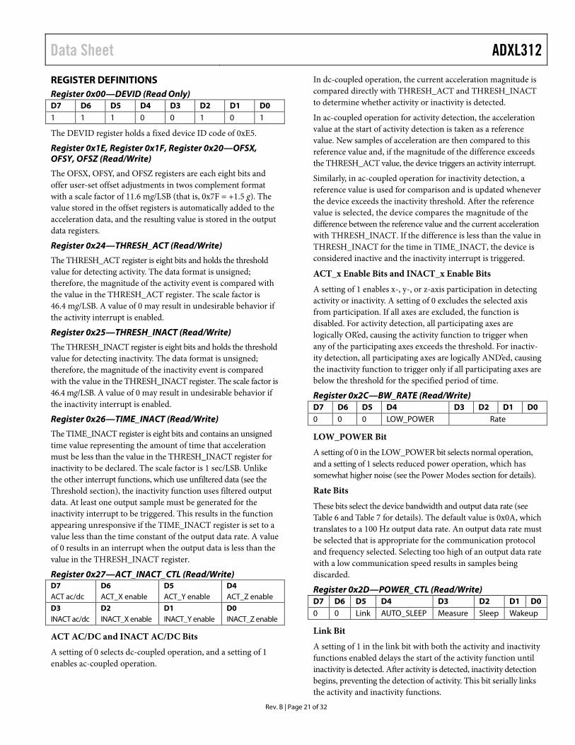
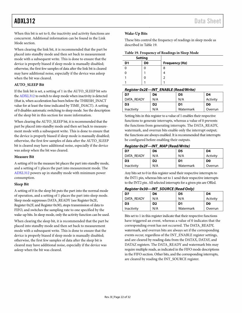
DATA FORMATTING OF UPPER DATA RATES Formatting of output data at the 3200 Hz and 1600 Hz output data rates changes depending on the mode of operation (full-resolution or fixed 10-bit) and the selected output range.
When in full-resolution or ±1.5 g, 10-bit operation, the LSB of the output data-word is always 0. When data is right justified, this corresponds to Bit D0 of the DATAx0 register, as shown in Figure 33. When data is left justified and the part is operating in ±1.5 g, 10-bit mode, the LSB of the output data-word is Bit D6 of the DATAx0 register. In full-resolution operation when data is left justified, the location of the LSB changes according to the selected output range.
For a range of ±1.5 g, the LSB is Bit D6 of the DATAx0 register; for ±3 g, Bit D5 of the DATAx0 register; for ±6 g, Bit D4 of the DATAx0 register; and for ±12 g, Bit D3 of the DATAx0 register. This is shown in Figure 34.
The use of 3200 Hz and 1600 Hz output data rates for fixed 10-bit operation in the ±3 g, ±6 g, and ±12 g output ranges provides an LSB that is valid and that changes according to the applied accel-eration. Therefore, in these modes of operation, Bit D0 is not always 0 when output data is right justified, and Bit D6 is not always 0 when output data is left justified. Operation at any data rate of 800 Hz or lower also provides a valid LSB in all ranges and modes that changes according to the applied acceleration.
0D1D2D3D4D5D6D7
D0D1D2D3D4D5D6D7D0D1D2D3D4D5D6D7
D0D1D2D3D4D5D6D7DATAx1 REGISTER DATAx0 REGISTER
OUTPUT DATA-WORD FOR±12g, FULL-RESOLUTION MODE. OUTPUT DATA-WORD FOR ±1.5g, 10-BIT
AND ±1.5g, FULL-RESOLUTION MODES.
THE ±3g AND ±6g FULL-RESOLUTION MODES HAVE THE SAME LSB LOCATION AS THE±1.5gAND ±12g FULL-RESOLUTION MODES, BUT THE MSB LOCATION CHANGES TO BIT D2 ANDBIT D3 OF THE DATAx1 REGISTER FOR ±3g AND ±6g, RESPECTIVELY. 08
791-
145
Figure 33. Data Formatting of Full-Resolution and ±1.5 g, 10-Bit Modes of Operation When Output Data Is Right Justified
0D1D2D3D4D5D6D7
D0D1D2D3D4D5D6D7D0D1D2D3D4D5D6D7
D0D1D2D3D4D5D6D7DATAx1 REGISTER DATAx0 REGISTER
MSB FOR ALL MODESOF OPERATION WHENLEFT JUSTIFIED.
LSB FOR ±1.5g, FULL-RESOLUTIONAND ±1.5g, 10-BIT MODES.
LSB FOR ±3g, FULL-RESOLUTION MODE.LSB FOR ±6g, FULL-RESOLUTION MODE.
LSB FOR ±12g, FULL-RESOLUTION MODE.
FOR 3200Hz AND 1600Hz OUTPUT DATA RATES, THE LSB IN THESE MODES IS ALWAYS 0.ADDITIONALLY, ANY BITS TO THE RIGHT OF THE LSB ARE ALWAYS 0 WHEN THE OUTPUTDATA IS LEFT JUSTIFIED. 08
791-
146
Figure 34. Data Formatting of Full-Resolution and ±1.5 g, 10-Bit Modes of Operation When Output Data Is Left Justified
ADXL312 Data Sheet
Rev. B | Page 28 of 32
NOISE PERFORMANCE The specification of noise shown in Table 1 corresponds to the best case noise of the ADXL312 in normal power operation (LOW_POWER bit = 0 in BW_RATE register, Address 0x2C). For normal power operation at data rates below 100 Hz, the noise of the ADXL312 is equivalent to the noise at 100 Hz ODR in LSBs. For data rates greater than 100 Hz, the noise increases roughly by a factor of √2 per doubling of the data rate. For example, at 400 Hz ODR, the noise on the x- and y-axes is typically less than 2.0 LSB rms and the noise on the z-axis is typically less than 3.0 LSB rms.
For low power operation (LOW_POWER bit = 1 in BW_RATE register, Address 0x2C) the noise of the ADXL312 is constant for all valid data rates shown in Table 7. This value is typically less than 2.4 LSB rms for the x- and y-axes and typically less than 3.5 LSB rms for the z-axis.
Figure 35 shows the typical Allan deviation for the ADXL312. The 1/f corner of the device, as shown in this figure, is very low, allowing absolute resolution of approximately 100 µg (assuming there is sufficient integration time). The figure also shows that the noise density is 340 µg/√Hz for the x- and y-axes and 470 µg/√Hz for the z-axis.
0.01 0.1 1 10 100 1k 10k10
100
1k
10k
AVERAGING PERIOD, (s)
ALL
AN
DEV
IATI
ON
(µg)
X-AXISY-AXISZ-AXIS
0879
1-25
1
Figure 35. Root Allan Deviation
70
80
90
100
110
120
130
2.0 2.2 2.4 2.6 2.8 3.0 3.2 3.4 3.6
SUPPLY VOLTAGE, VS (V)
PER
CEN
TAG
E O
F N
OR
MA
LIZE
D N
OIS
E (%
)
X-AXISY-AXISZ-AXIS
0879
1-25
2
Figure 36. Normalized Noise vs. Supply Voltage, VS

Data Sheet ADXL312
Rev. B | Page 29 of 32
AXES OF ACCELERATION SENSITIVITY AZ
AY
AX 0879
1-04
2
Figure 37. Axes of Acceleration Sensitivity (Corresponding Output Voltage Increases When Accelerated Along the Sensitive Axis)
GRAVITY
XOUT = +1gYOUT = 0gZOUT = 0g
XOUT = –1gYOUT = 0gZOUT = 0g
TOP
XOUT = 0gYOUT = +1gZOUT = 0g
TOP
XOUT = 0gYOUT = –1gZOUT = 0g TO
P
XOUT = 0gYOUT = 0gZOUT = +1g
XOUT = 0gYOUT = 0gZOUT = –1g
TOP
0879
1-04
3
Figure 38. Output Response vs. Orientation to Gravity
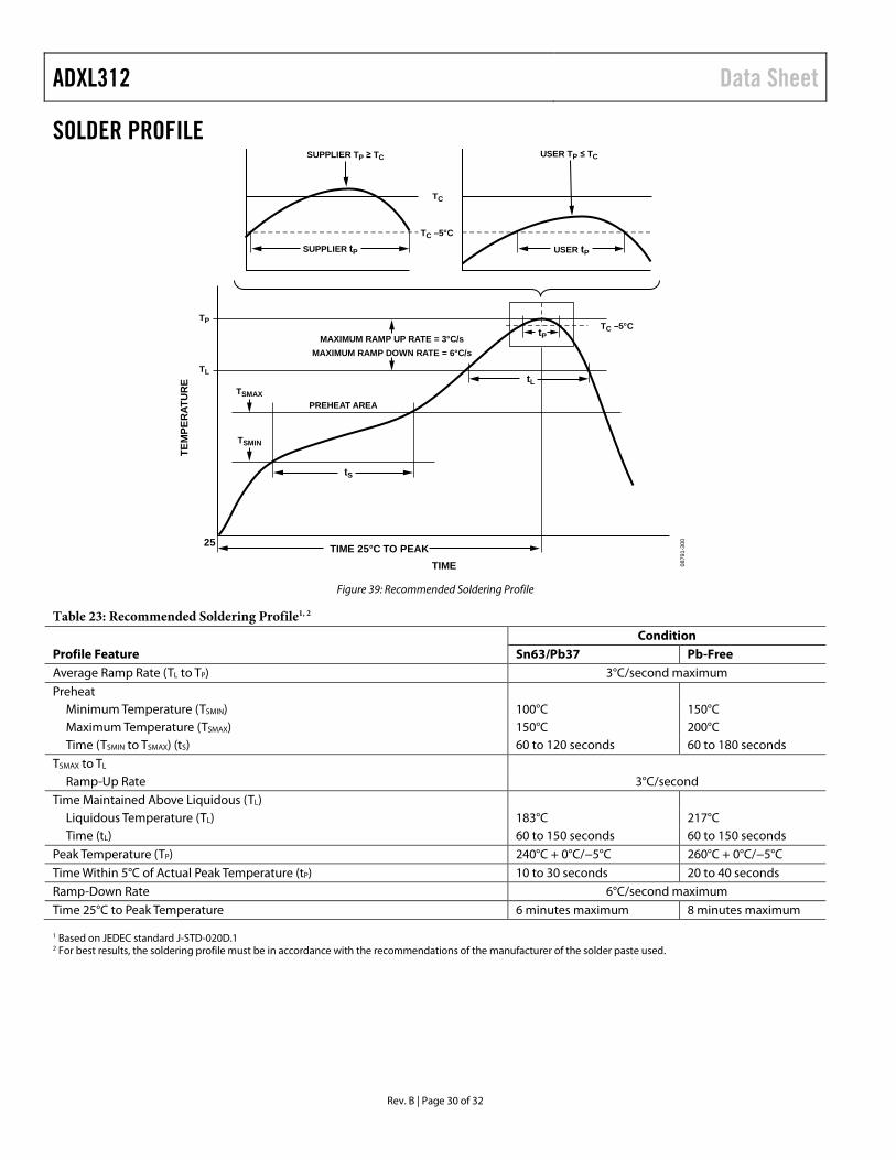
ADXL312 Data Sheet
Rev. B | Page 30 of 32
SOLDER PROFILE SUPPLIER TP ≥ TC
MAXIMUM RAMP UP RATE = 3°C/sMAXIMUM RAMP DOWN RATE = 6°C/s
PREHEAT AREA
TC
TC –5°C
TC –5°C
TSMAX
TL
TP
tP
tL
tS
USER TP ≤ TC
SUPPLIER tP USER tP
TEM
PER
ATU
RE
TIMETIME 25°C TO PEAK25
TSMIN
0879
1-30
0
Figure 39: Recommended Soldering Profile
Table 23: Recommended Soldering Profile1, 2
Profile Feature Condition
Sn63/Pb37 Pb-Free Average Ramp Rate (TL to TP) 3°C/second maximum Preheat
Minimum Temperature (TSMIN) 100°C 150°C Maximum Temperature (TSMAX) 150°C 200°C Time (TSMIN to TSMAX) (tS) 60 to 120 seconds 60 to 180 seconds
TSMAX to TL Ramp-Up Rate 3°C/second
Time Maintained Above Liquidous (TL) Liquidous Temperature (TL) 183°C 217°C Time (tL) 60 to 150 seconds 60 to 150 seconds
Peak Temperature (TP) 240°C + 0°C/−5°C 260°C + 0°C/−5°C Time Within 5°C of Actual Peak Temperature (tP) 10 to 30 seconds 20 to 40 seconds Ramp-Down Rate 6°C/second maximum Time 25°C to Peak Temperature 6 minutes maximum 8 minutes maximum 1 Based on JEDEC standard J-STD-020D.1 2 For best results, the soldering profile must be in accordance with the recommendations of the manufacturer of the solder paste used.
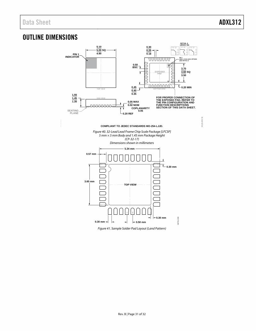
Data Sheet ADXL312
Rev. B | Page 31 of 32
OUTLINE DIMENSIONS
1
0.50BSC
PIN 1INDICATOR
32
916
17
24
25
8
0.05 MAX0.02 NOM
0.20 REF
COPLANARITY0.05
0.300.250.18
5.105.00 SQ4.90
1.551.451.35
0.450.400.35
0.20 MIN
3.703.60 SQ3.50
COMPLIANT TO JEDEC STANDARDS MO-254-LJJD. 03-2
0-20
17-B
BOTTOM VIEWTOP VIEW
PKG
-003
616
SEATINGPLANE
EXPOSEDPAD
END VIEW
PIN 1INDIC ATOR AREA OPTIONS(SEE DETAIL A)
DETAIL A(JEDEC 95)
FOR PROPER CONNECTION OFTHE EXPOSED PAD, REFER TOTHE PIN CONFIGURATION ANDFUNCTION DESCRIPTIONSSECTION OF THIS DATA SHEET.
Figure 40. 32-Lead Lead Frame Chip Scale Package [LFCSP]
5 mm × 5 mm Body and 1.45 mm Package Height (CP-32-17)
Dimensions shown in millimeters
0879
1-03
8
0.30 mm
0.30 mm0.30 mm 0.50 mm
3.60 mm
5.34 mm
0.57 mm
TOP VIEW
Figure 41. Sample Solder Pad Layout (Land Pattern)

ADXL312 Data Sheet
Rev. B | Page 32 of 32
ORDERING GUIDE
Model1, 2 Measurement Range Specified Voltage (V)
Temperature Range Package Description
Package Option
ADXL312WACPZ ±1.5 g, ±3 g, ±6 g, ±12 g 3.3 −40°C to +105°C 32-Lead LFCSP CP-32-17 ADXL312WACPZ-RL ±1.5 g, ±3 g, ±6 g, ±12 g 3.3 −40°C to +105°C 32-Lead LFCSP CP-32-17 ADXL312ACPZ ±1.5 g, ±3 g, ±6 g, ±12 g 3.3 −40°C to +105°C 32-Lead LFCSP CP-32-17 ADXL312ACPZ-RL ±1.5 g, ±3 g, ±6 g, ±12 g 3.3 −40°C to +105°C 32-Lead LFCSP CP-32-17 EVAL-ADXL312Z Evaluation Board 1 Z = RoHS Compliant Part 2 W = Qualified for Automotive Applications
AUTOMOTIVE PRODUCTS The ADXL312W models are available with controlled manufacturing to support the quality and reliability requirements of automotive applications. Note that these automotive models may have specifications that differ from the commercial models; therefore, designers should review the Specifications section of this data sheet carefully. Only the automotive grade products shown are available for use in automotive applications. Contact your local Analog Devices account representative for specific product ordering information and to obtain the specific Automotive Reliability reports for these models.
I2C refers to a communications protocol originally developed by Philips Semiconductors (now NXP Semiconductors).
©2010–2017 Analog Devices, Inc. All rights reserved. Trademarks and registered trademarks are the property of their respective owners. D08791-0-4/17(B)