digital design strategies and techniques. analog building blocks for digital primitives we implement...
TRANSCRIPT

Digital Design Strategies and Techniques
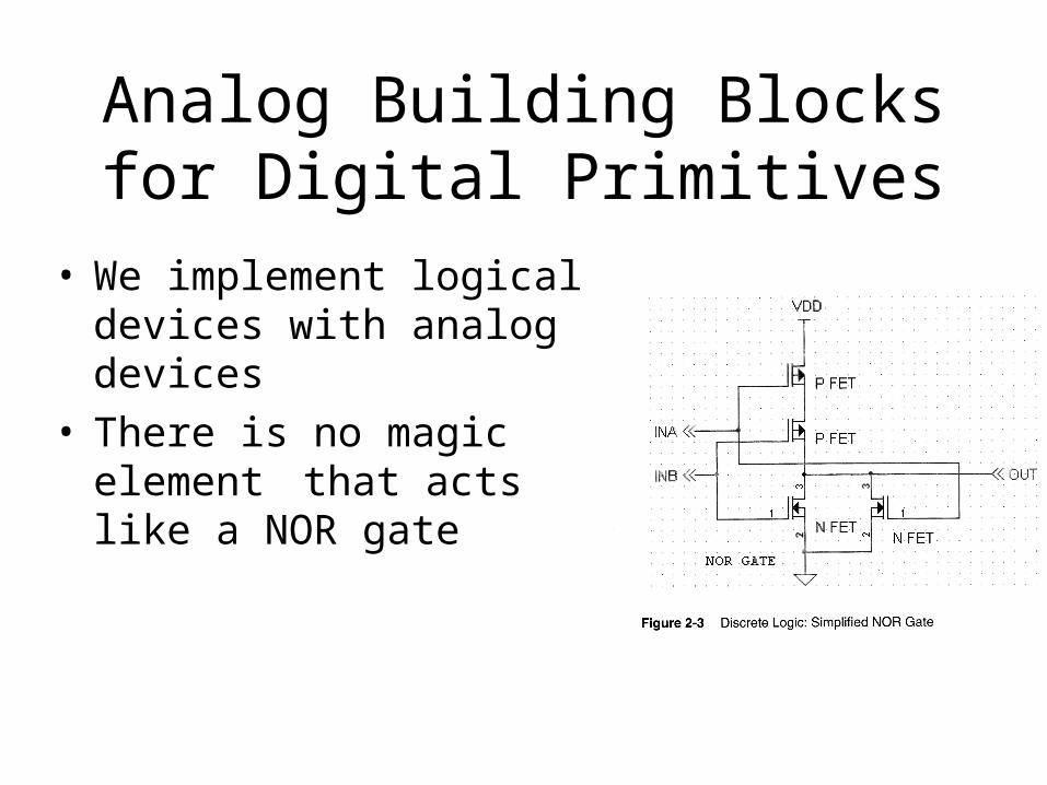
Analog Building Blocks for Digital Primitives
• We implement logical devices with analog devices
• There is no magic elementthat acts like a NOR
gate

Using a LUT to Implement Logic Function
• Most FPGA use a multiplexer(MUX) Look-Up Table (LUT) as a basic logical element
• The LUT is a versatile• The LUT is efficiently
implemented in silicon

Synthesis Example Overheat Detection

Synthesis Example Overheat Detection

Synthesis Example Overheat Detection

Synthesis Example Overheat Detection

Discussion of Design Processing Steps
• Syntax checking• It makes good sense to have several tools available for
checking your code• Design minimization and optimization• Minimizing the Boolean expression• Recognizing and removing redundant logic terms• The design is converted to a netlist• The design elements are linked together• Black-box modules are replaced with library element• Floor planning and routing


Shifty Logical Circuits
• The output is very likely to be glitchy when the input is changed
• The input is noisy signal that crosses the input threshold
• Use hysteresis

• A parasite RC network delay the input signal
• Use a synchronous flipflop
RC networks

Synchronous Logic Rules
• Metastability• The setup time is the time period before clock edge
of the synchronizing clock when the input is required to be stable
• The hold time is the time period after the synchronizing clock edge when the input is required to be stable
• If signal is changed between setup-hold window output is neither 1 nor 0
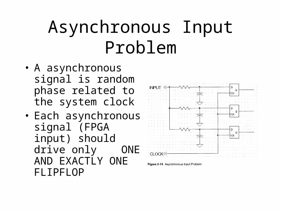
Asynchronous Input Problem
• A asynchronous signal is random phase related to the system clock
• Each asynchronous signal (FPGA input) should drive only ONE AND EXACTLY ONE FLIPFLOP
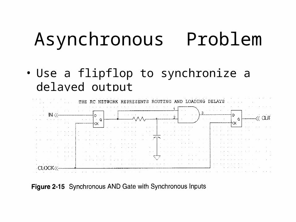
Asynchronous Problem
• Use a flipflop to synchronize a delayed output

Clock frequency
• Divide-by-Two circuit• Rising edge of the
clock must not occur before setup_time + output_delay + routing_delay
• The input clock had better not
have frequency greater that 333.333 MHz
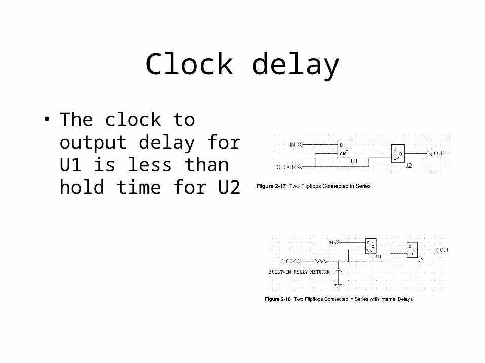
Clock delay
• The clock to output delay for U1 is less than hold time for U2

Clock Skew
• Two flipflop connected in series
• If the clock skew is too long, then we’ll get the new value of U1 or we’ll violate the output of U2

Handling External Signals
• Signal arrive at synchronizing flipflop at different time
• Using a alternative clock edge

Logic Minimization
• A synchronizer will recognize and remove the redundant logical rules
input test1,test2,test3;
output sample;
sample = (test1&test2&test3) |
(test1&!test2&test3) |
(test1&test2& !test3);
= test1 & (test2|test3);

Logic Minimization
• The designers uses the synchronous techniques
• The ability of synthesizer is limited
• The synthesizer will not find the redundancy
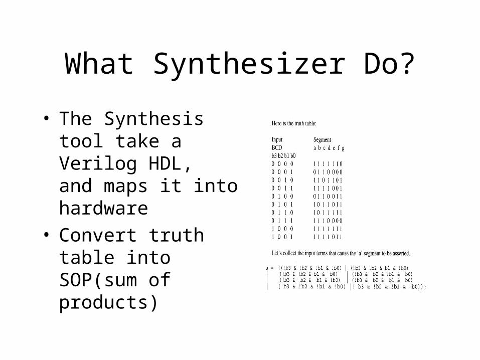
What Synthesizer Do?
• The Synthesis tool take a Verilog HDL,and maps it into hardware
• Convert truth table into SOP(sum of products)

Area/Delay optimization
• The designers workwill not be judged how perfect it is
• The goal of your quest is to achieve ‘good enough ‘
• The expired designers always a way out of a problem by insuring that a faster or denser device is available in the same device footprint