
www.elsevier.com/locate/apsusc
Available online at www.sciencedirect.com
Applied Surface Science 254 (2008) 3509–3516
Gas barrier properties of titanium oxynitride films deposited on
polyethylene terephthalate substrates by reactive magnetron sputtering
M.-C. Lin a, L.-S. Chang a,*, H.C. Lin b
a Department of Materials Science and Engineering, National ChungHsin University, 250, Kuo-Kung Road, 40227 Taichung, Taiwan, ROCb Department of Materials Science and Engineering, National Taiwan University, 1, Roosevelt Road, Sec. 4, 106 Taipei, Taiwan, ROC
Received 22 August 2007; received in revised form 23 November 2007; accepted 23 November 2007
Available online 15 December 2007
Abstract
Titanium oxynitride (TiNxOy) films were deposited on polyethylene terephthalate (PET) substrates by means of a reactive radio frequency (RF)
magnetron sputtering system in which the power density and substrate bias were the varied parameters. Experimental results show that the
deposited TiNxOy films exhibited an amorphous or a columnar structure with fine crystalline dependent on power density. The deposition rate
increases significantly in conjunction as the power density increases from 2 W/cm2 to 7 W/cm2. The maximum deposition rate occurs, as the
substrate bias is�40 Vat a certain power densities chosen in this study. The film’s roughness slightly decreases with increasing substrate bias. The
TiNxOy films deposited at power densities above 4 W/cm2 show a steady Ti:N:O ratio of about 1:1:0.8. The water vapor and oxygen transmission
rates of the TiNxOy films reach values as low as 0.98 g/m2-day-atm and 0.60 cm3/m2-day-atm which are about 6 and 47 times lower than those of
the uncoated PET substrate, respectively. These transmission rates are comparable to those of DLC, carbon-based and Al2O3 barrier films.
Therefore, TiNxOy films are potential candidates to be used as a gas permeation barrier for PET substrate.
# 2007 Elsevier B.V. All rights reserved.
Keywords: Titanium oxynitride; Sputtering; Polyethylene terephthalate (PET); Gas permeation
1. Introduction
The increased demand in portable devices, for example, the
flexible displays and thin film batteries used in note book
computers, mobile phones and various electronic instruments,
has led to a great deal of work pertaining to the development of
suitable substrate materials. These substrate materials are
required to possess certain properties, such as portability,
durability, flexibility and optical transparency. To meet these
requirements, polymers are considered to be the most
appropriate material. Nevertheless, most polymer substrates
have some drawbacks. One of the most critical properties of
polymer substrates which need to be addressed in order to
achieve successful operations is their insufficient resistance to
gas permeation.
The deposition of diamond-like carbon (DLC) [1–4],
carbon-based [5,6] and metal oxide films [7–9] have been
* Corresponding author. Tel.: +886 4 2284 0500/406; fax: +886 4 2285 2433.
E-mail address: [email protected] (L.S. Chang).
0169-4332/$ – see front matter # 2007 Elsevier B.V. All rights reserved.
doi:10.1016/j.apsusc.2007.11.064
considered to be a promising technique to improve the
properties of polymer substrates used in portable devices by
enhancing their resistance to abrasive wear, gas permeation,
chemical attack, etc. These DLC, carbon-based and metal oxide
films can be successfully deposited by magnetically enhanced
chemical vapor deposition, plasma-source ion implantation, RF
low-pressure glow discharge, magnetron sputtering and
microwave techniques. An alternative coating materials class
that may merit consideration are transition-metal oxynitrides
(TMeNxOy), which, due to their colorific and optical properties,
chemical stability and good adhesion to polymers, have
previously been widely employed as a wear resistant, anti-
reflective, decorative and/or diffusion barrier coating for
polymer components [10–15]. TiNxOy films are representative
transition-metal oxynitrides and can be deposited onto
substrates by various coating techniques, which include
magnetron sputtering [10,11], ion assisted deposition [14],
and evaporation [15]. Magnetron sputtering is considered to be
more advantageous among these different deposition techni-
ques due to its low processing temperature, dense deposited
film, moderate set up cost and high stability in control.

M.-C. Lin et al. / Applied Surface Science 254 (2008) 3509–35163510
Polyethylene terepthalate (PET) is one of the most promising
polymers being used as flexible substrate due to its excellent
optical transparency, chemical stability, high durability and low
cost. However, to the author’s knowledge, no related paper which
investigated the deposition of TiNxOy films on PET substrates has
been reported. In this study, the TiNxOy films were deposited on
PET substrates by RF reactive magnetron sputtering. The
influences of power density and applied substrate bias on the
deposition rate, gas permeation rate, microstructure and
composition of the TiNxOy films were investigated.
2. Experimental details
TiNxOy films were deposited by means of a reactive
magnetron sputtering system (made by Junsun Corporation,
Taiwan). A 5 cm diameter, 99.999% pure titanium target was
used. The PET substrate, a C10–H8–O4 compound with 3–6%
humidity (product no: BD11, Nan-Yan Corporation, Taiwan)
had a thickness of 100 mm. The substrate to target distance was
kept at 15 cm and the holder was rotated at a speed of 10 rpm to
improve the film homogeneity. Argon was used as the sputter
gas and nitrogen as the reactive gas during sputtering.
Depositions were carried out in pure Ar and Ar/N2 mixtures.
Meanwhile, oxygen atoms existing residually in chamber or
coming from the PET substrate would contribute to form the
TiNxOy films during deposition. The sputtering parameters used
in this study are listed in Table 1, in which the power density
and dc substrate bias varied while the other parameters were
fixed. To clean the substrate surface prior to the deposition and
improve film’s adhesion, the PET surface was plasma pre-
treated in a sputtering chamber for 10 min with a direct current
(dc) bias of �300 V, which is generated by an MP-1 advanced
converter magnetron power supply. The pre-treatment was
carried out by using Ar gas with a pressure of 1.8 Pa. The same
power supply is used for both pre-treatment of substrate and
sputtering process, although their amounts of dc bias were
different. The dc bias is applied between the stainless holder
and stainless chamber wall. Although the electrical conductiv-
ity of the TiNxOy film is low, the dc bias between the PET
substrate and stainless chamber wall can exhibit sufficient
effect on the film deposition.
The water vapor and oxygen transmission rates of
uncoated and TiNxOy coated PET were measured by a
Permatran-w 3/61 and an Ox-Tran 2/61model system (made
by MOCON Instrument), respectively. The sample area was
Table 1
The sputtering parameters used in this study
Target Ti target (99.999% purity) with diameter of 5 cm
Substrate PET
Power density 2 W/cm2, 4 W/cm2, 6 W/cm2, 7 W/cm2
dc substrate bias 0 V, �20 V, �40 V, �60 V
Gas flow ratio Ar:N2 = 3:2
Base pressure 1.33 � 10�3 Pa
Working pressure 1.33 � 10�1 Pa
Deposition time 60 min
4.5 cm � 4.5 cm. Both transmission rate measurements were
carried out at atmospheric pressure and 40 8C, and under relative
humidity of 100% and 0%, respectively. A multi-function
scanning probe microscope (SPM, NS4 D3100CL Digital
Instrument) was used to measure the film’s roughness. A Si
tip with a radius of 10 nm was used for this analysis. The scanned
sample area was 1 mm2 and the scanning speed was 1 Hz.
The field-emission scanning electron microscope (FESEM,
JSM-6700F, JEOL) for studying the coating morphology and
microstructure was operated at 1 keV accelerating voltage. The
TiNxOy surface was coated with a thin platinum layer for SEM
observation to prevent charging during FESEM analysis. The
crystal structures and chemical compositions of deposited
TiNxOy films were analyzed by means of a high-resolution
transmission electron microscope (HRTEM, JEOL-3010,
operated at 200 keV) and X-ray photoelectron spectroscopy
(XPS, Theta Probe, VG), respectively. The XPS spectra were
obtained using Al Ka X-rays operated at 15 kVand 400 W. The
Ti, N and O concentrations in films were quantified from the
areas under the Ti 2p, N 1s and O 1s characteristic signals in the
photoelectron spectrum, after carrying out the Shirley back-
ground subtraction. Relative sensitivity factors provided by the
manufacturer were employed. The sampling size and surface
etching time were 1 cm2 and 30 s, respectively. The pressure in
the analysis chamber was 8 � 10�8 Pa. The thicknesses of the
TiNxOy films deposited on pure silicon substrates placed
alongside the PET substrates were measured by means of an a-
step profiler (Dektak3 ST, Veeco).
3. Results and discussion
3.1. Chemical composition and microstructure
Fig. 1 shows the XPS spectra of TiNxOy films deposited on
PET substrates at various power densities and with a fixed
substrate bias of �40 V. The deposited films were cleaned
before XPS analysis to prevent them from contamination by
adventitious oxygen. The analysis of XPS spectra in Fig. 1
indicates that Ti, N and O elements coexist in the deposited
TiNxOy films. The appearance of O element is consistent with
the reported studies on titanium oxynitride and aluminum
oxynitride films by Guillot et al. [16] and Dreer et al. [17]. Their
films were also deposited in a sputter chamber with very little or
even no oxygen content. This indicates that at a base pressure of
5 � 10�6 Pa or even below, there is enough oxygen present to
partake in the reaction with Ti and N atoms to form the TiNxOy
films. In this work, the H2O molecules which adhere on the
surface or exist in the interior of PET substrates [18], and the
residual O2 impurity in the sputter chamber, are expected to
provide the O atoms during the deposition of TiNxOy films.
Fig. 2(a–c) shows the XPS Ti 2p lines of TiNxOy films
deposited onto PET at various power densities with a fixed
substrate bias of �40 V. As shown in Fig. 2(a), there occurs a
predominant Ti–O2 bonding for the film deposited at a power
density of 2 W/cm2. By increasing power density to 4 W/cm2 or
7 W/cm2, there occurs both Ti–N and Ti–O2 bonding in the
deposited film, as shown in Fig. 2(b–c). This feature can be

Fig. 1. XPS spectra of TiNxOy films deposited on PET with a fixed substrate bias of �40 V at various power densities. (a) 2 W/cm2, (b) 4 W/cm2, (c) 6 W/cm2, (d)
7 W/cm2.
M.-C. Lin et al. / Applied Surface Science 254 (2008) 3509–3516 3511
explained as below. At a low power density of 2 W/cm2, less
quantity of Ti atoms are sputtered from the Ti target, and some
Ti ions are created after sputtering due to charge exchange.
These Ti atoms (ions) will first react with O due to their strong
affinity. Therefore, the deposited film is mainly comprised of Ti
and O elements. With increasing power density, more Ti atoms
are sputtered from Ti target and more Ti ions are created due to
charge exchange. There is more opportunity to form the Ti–N
bonding besides of the Ti–O2 bonding. Therefore, the XPS
spectra intensities of Ti and N elements maintain steady values
at higher power densities, as shown in Fig. 1(b–d) and Fig. 2(b–
c). Based on the quantitative analysis of XPS, the compositions
of TiNxOy films deposited at various power densities are
presented in Fig. 3. As can be seen in Fig. 3, the TiNxOy films
deposited at power densities above 4 W/cm2 show a steady
Ti:N:O ratio of about 1:1:0.8.
Fig. 4(a–c) shows the HR-TEM cross-sectional images and
diffraction patterns of TiNxOy films deposited onto PET at
various power densities with a fixed substrate bias of �40 V. In
Fig. 4(a), the TiNxOy film deposited at power densities of 2 W/
cm2 exhibits an amorphous structure. Increasing the power
density to higher than 4 W/cm2, the TiNxOy film exhibits a
columnar structure with fine crystalline, as shown in Fig. 4(b–
c). The occurrence of columnar structure with fine crystalline in
TiNxOy films may be ascribed to the rising of substrate
temperature during the deposition process. The bombardment
of the sputtered atoms (ions) will raise the substrate
temperature during the deposition of TiNxOy films. At a higher
power density, more sputtered atoms (ions) are bombarded onto
the PET substrate and the substrate temperature is increased to a
higher one. In the present study, the substrate temperature
during deposition can reach about 80 8C at a power density of
7 W/cm2. This rising of substrate temperature will exhibit
sufficient driving force for columnar structure to with fine
crystalline. As illustrated clearly in Fig. 4(b) and (c), the higher
the power density, the more obvious the columnar structure
with fine crystalline. Besides, it is worthy to mention that the
indistinct trace surrounding the surface of these columnar
structures in Fig. 4(b–c) is only a false image introduced during
the preparation of TEM specimens.

Fig. 2. The XPS Ti 2p lines of TiNxOy films deposited onto PET at various power densities and with a fixed substrate bias of �40 V.
M.-C. Lin et al. / Applied Surface Science 254 (2008) 3509–35163512
3.2. Deposition rate
Fig. 5 shows the deposition rates of TiNxOy films deposited
at various power densities and substrate biases. It is found that
the deposition rate increases significantly with increasing
power density. The deposition rate increases 4–9 times,
depending on the power density in the range of 2–7 W/cm2.
This phenomenon can be explained as follows. At higher power
density, more Ar+ and N2+ ions are generated to impact the
titanium target and more Ti atoms (ions) are sputtered out and
react with N and O atoms in the plasma to form TiNxOy and
deposit onto the PET substrate. Hence, the deposition rate of
TiNxOy film increases with increasing power density.
One can also find, in Fig. 5, that the deposition rate increases
slightly from 0 V to �20 V bias, reaches a maximum at �40 V
bias, and then decreases at�60 V bias. Actually, proper supply
of substrate bias (such as �20 V to �40 V) will raise the
negative potential between the ground and substrate. Ti ions are
more guided onto the substrate surface due to this negative
potential. Besides, the moving direction of other species (Ti and
N atoms) will also be more confined to around the substrate due
to the collision with these guided Ti ions. All these effects will
increase the adhesion of deposited species onto the substrate,
and hence increase the film’s deposition rate. [19,20]. However,
an over-high substrate bias (such as �60 V) will produce a
significant drop of electrical potential in the plasma. This will
make the species (atoms or ions) have over-high impact energy
and induce re-sputtering, and hence the deposition rate of
TiNxOy film decreases significantly. It is worthy to mention that
the maximum deposition rate of TiNxOy films, shown in Fig. 5,
is only about 1.2 nm/min, which is much lower than those of
DLC (750 nm/min) [1], carbon-based (21 nm/min) and Al2O3
(51 nm/min) films [5,7].
3.3. Surface morphology and roughness
Fig. 6(a–d) shows the FESEM micrographs of TiNxOy films
deposited onto PET at various power densities and without
substrate bias. As shown in Fig. 6(a), many small pinholes
appear in the TiNxOy film prepared at a power density of 2 W/

Fig. 3. Chemical compositions of TiNxOy films deposited onto PET at various
power densities and with a fixed substrate bias of �40 V.
Fig. 5. Deposition rates of TiNxOy films on PET in dependence of the substrate
bias at various power densities (film thickness = deposition rate � 60).
Fig. 4. HR-TEM cross-sectional images and diffraction patterns of TiNxOy films deposited onto PET at various power densities with a fixed substrate bias of�40 V.
M.-C. Lin et al. / Applied Surface Science 254 (2008) 3509–3516 3513
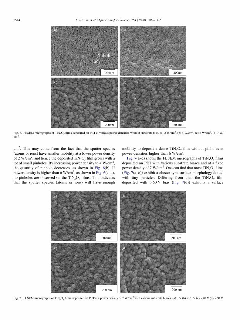
Fig. 6. FESEM micrographs of TiNxOy films deposited on PET at various power densities without substrate bias. (a) 2 W/cm2, (b) 4 W/cm2, (c) 6 W/cm2, (d) 7 W/
cm2.
M.-C. Lin et al. / Applied Surface Science 254 (2008) 3509–35163514
cm2. This may come from the fact that the sputter species
(atoms or ions) have smaller mobility at a lower power density
of 2 W/cm2, and hence the deposited TiNxOy film grows with a
lot of small pinholes. By increasing power density to 4 W/cm2,
the quantity of pinhole decreases, as shown in Fig. 6(b). If
power density is higher than 6 W/cm2, as shown in Fig. 6(c–d),
no pinholes are observed on the TiNxOy films. This indicates
that the sputter species (atoms or ions) will have enough
Fig. 7. FESEM micrographs of TiNxOy films deposited on PET at a power density of
mobility to deposit a dense TiNxOy film without pinholes at
power densities higher than 6 W/cm2.
Fig. 7(a–d) shows the FESEM micrographs of TiNxOy films
deposited on PET with various substrate biases and at a fixed
power density of 7 W/cm2. One can find that most TiNxOy films
(Fig. 7(a–c)) exhibit a cluster-type surface morphology dotted
with tiny particles. Differing from that, the TiNxOy film
deposited with �60 V bias (Fig. 7(d)) exhibits a surface
7 W/cm2 with various substrate biases. (a) 0 V (b)�20 V (c)�40 V (d)�60 V.

Fig. 8. RMS roughness of TiNxOy films deposited on PET in dependence of the
substrate bias. The power density was 7 W/cm2.
M.-C. Lin et al. / Applied Surface Science 254 (2008) 3509–3516 3515
morphology without those closely dotted tiny particles. This
feature is ascribed to the fact that the species (atoms or ions) in
the plasma with �60 V bias have over-high impact energy to
bombard the surface of TiNxOy films. This intense bombard-
ment may impinge away those tiny particles on TiNxOy films,
although some of those tiny particles may be incorporated in the
film during the continuous deposition process. This phenom-
enon is consistent with the result of the re-sputtering effect
discussed in Section 3.2.
The values of root-mean-square (RMS) roughness of TiNxOy
films deposited on PET with various substrate biases, measured
by using the scanning probe microscope, are presented in Fig. 8.
The film’s surface roughness decreases with increasing
Fig. 9. (a) WVTR and (b) OTR of TiNxOy films coated PET in dependence of the substrate biases and power densities.
substrate bias. The kinetic energy of depositing atoms is
increased at higher substrate bias. These depositing atoms with
higher kinetic energy will easily move into the space between
clusters and hence the TiNxOy films can exhibit smoother
surface morphologies at higher substrate bias. The re-sputtering
effect at higher substrate bias also smoothens the film surface as
shown in Fig. 7(d).
3.4. Gas permeation
The water vapor transmission rate (WVTR) and oxygen
transmission rate (OTR) of TiNxOy films coated PET in
dependence on power densities and substrate biases are plotted
in Fig. 9(a) and (b), respectively. The WVTR and OTR of
uncoated PET are 5.53 g/m2-atm-day and 28.09 cm3/m2-atm-
day, respectively. It can be clearly seen in Fig. 9(a–b) that the
WVTR and OTR of the PET substrates reduce significantly
after the deposition of TiNxOy films. From these two figures, it
can be concluded that both the film’s thickness and quality,
resulting from the different power densities and substrate
biases, have important effects on the film’s resistance against
gas permeation.
As already mentioned, the deposition rate of TiNxOy film
increases with increasing power density, and hence the film
thickness and consequent resistance against permeation of
water vapor and oxygen also increase. It has also been shown in
Fig. 5 that, the deposition rate reaches a maximum at �40 V
bias and then decreases due to re-sputtering at�60 V bias. This
feature can explain why the WVTR and OTR reduce as the
substrate bias changes from 0 V to �40 V, and then rise as the
bias ranges from �40 V to�60 V, as shown in Fig. 9. All these
results exhibit that a thicker TiNxOy film will be a better gas
barrier [21,22]. In Fig. 9, the OTR of TiNxOy films deposited at
power density of 2 W/cm2 is found to have almost the same
value as that of uncoated PET substrate. This phenomenon is
understandable and can be explained as below. As shown in
Fig. 6(a), TiNxOy films deposited at power density of 2 W/cm2

M.-C. Lin et al. / Applied Surface Science 254 (2008) 3509–35163516
have many small pinholes. These small pinholes act as the
shortcut for oxygen permeation, and these films have high OTR
values. It is worthwhile mentioning that these small pinholes
existing in TiNxOy films still have an effective resistance to
water vapor, so their WVTR still maintains a quite low value
(Fig. 9(a)).
As discussed above, properly deposited TiNxOy films can
significantly improve the barrier properties of PET substrates.
In this study, the optimal sputtering parameters in depositing
excellent TiNxOy films are power density of 7 W/cm2 and
�40 V substrate bias. The water vapor and oxygen transmission
rates of these optimal TiNxOy films reach values as low as
0.98 g/m2-day-atm and 0.60 cm3/m2-day-atm, respectively.
These values of WVTR and OTR are about 6 and 47 times
lower than those of the uncoated PET substrate.
It is valuable to compare briefly the gas permeation
resistance of TiNxOy films and those currently used DLC,
carbon-based and Al2O3 films. As presented above, the water
vapor and oxygen transmission rates of the TiNxOy films
prepared in this study can reach optimal values of 0.98 g/m2-
day-atm and 0.60 cm3/m2-day-atm, respectively. In the
reported studies, the oxygen transmission rates of DLC and
carbon-based films are about 0.4–4.5 cm3/m2-day-atm [1–4]
and 5.7 cm3/m2-day-atm [6], respectively, and the water
transmission rate of Al2O3 is about 1.12 g/m2-day-atm [7].
Hence, based on these data, the TiNxOy films can exhibit similar
or even higher resistance of gas permeation as compared to
DLC, carbon-based and Al2O3 barrier films. Namely, TiNxOy
films are potential candidates to be used as a gas permeation
barrier. Meanwhile, the TiNxOy films can have better electric
conductivity than Al2O3 films, higher mechanical property than
carbon-based films and their manufacturing cost is lower than
that of DLC films.
4. Conclusions
TiNxOy films have been successfully deposited on PET
substrates by means of the RF reactive magnetron sputtering
technique. The influences of power density and substrate bias
on the film’s properties are investigated. The TiNxOy film
deposited at power density of 2 W/cm2 exhibits an amorphous
structure. With increasing power density to be higher than 4 W/
cm2, the TiNxOy film exhibits a columnar structure with fine
crystalline. The deposition rate of TiNxOy film has an increment
of 4–9 times, when the power density rises from 2 W/cm2 up to
7 W/cm2. The deposition rate reaches its maximum with the
substrate bias of �40 V at all power densities chosen in this
study. Most TiNxOy films exhibit a cluster-type surface
morphology with closely dotted tiny particles. Their surface
roughness decreases slightly with increasing substrate bias. A
lot of small pinholes are observed in TiNxOy films deposited at a
low power density of 2 W/cm2. The TiNxOy films deposited at
power densities above 4 W/cm2 show a steady Ti:N:O ratio of
about 1:1:0.8. The film’s resistance against gas permeation
increases with increasing film’s thickness and quality, resulting
from the different power densities and substrate biases. The
water vapor and oxygen transmission rates of the TiNxOy films
reach optimal values as low as 0.98 g/m2-day-atm and
0.60 cm3/m2-day-atm and these values are about 6 and 47
times lower than those of the uncoated PET substrate,
respectively, while the power density is 7 W/cm2 and substrate
bias is �40 V. As compared to DLC, carbon-based and Al2O3
barrier films, the sputtered TiNxOy films can exhibit similar or
even higher resistance of gas permeation. Besides, the TiNxOy
films can have better electric conductivity than Al2O3 films,
higher mechanical property than carbon-based films and their
manufacturing cost is lower than that of DLC films.
Acknowledgement
This work was financially supported by the National Science
Committee (NSC) of Taiwan/ROC, under the auspices of the
Targeted Project (no. NSC93-2216-E-005-024).
References
[1] K. Inagawa, T. Zeniya, N. Hibino, Surf. Coat. Technol. 169/170 (2003)
344.
[2] S. Yamamoto, H. Kodama, T. Hasebe, A. Shirakura, T. Suzuki, Diamond
Relat. Mater. 14 (2005) 1112.
[3] M. Yoshida, S. Watanabe, T. Tanaka, T. Takagi, M. Shinohara, J.W. Lee,
Nucl. Instrum. Methods Phys. Res. B 206 (2003) 712.
[4] M. Yoshida, T. Tanaka, S. Watanabe, M. Shinohara, J.W. Lee, T. Takagi,
Surf. Coat. Technol. 174/175 (2003) 1033.
[5] S. Watanabe, M. Shinohara, H. Kodama, T. Tanaka, M. Yoshida, T. Takagi,
Thin Solid Films 420/421 (2002) 253.
[6] H. Kodama, A. Shinohara, A. Hotta, T. Suzuki, Surf. Coat. Technol. 201
(2006) 913.
[7] B.M. Henry, F. Dinelli, K.-Y. Zhao, C.R.M. Grovenor, O.V. Kolosov,
G.A.D. Briggs, A.P. Roberts, R.S. Kumar, R.P. Howson, Thin Solid Films
355/356 (1999) 500.
[8] M. Benmalek, H.M. Dunlop, Surf. Coat. Technol. 76/77 (1995) 821.
[9] A.S. da Silva Sobrinho, G. Czeremuszkin, M. Latreche, M.R. Wertheimer,
J. Vac. Sci. Technol. A 18 (2000) 149.
[10] F. Vaz, P. Cerqueira, L. Rebouta, S.M.C. Nascimento, E. Alves, Ph.
Goudeau, J.P. Riviere, K. Psichow, J. de Rijk, Thin Solid Films 447/
448 (2004) 449.
[11] M.H. Kazemeini, A.A. Berezin, N. Fukuhara, Thin Solid Films 372 (2000)
70.
[12] N. Martin, O. Banakh, A.M.E. Santo, S. Springer, R. Sanjines, J. Taka-
doum, F. Levy, Appl. Surf. Sci. 185 (2001) 123.
[13] F. Vaz, P. Cerqueira, L. Rebouta, S.M.C. Nascimento, E. Alves, Ph.
Goudeau, J.P. Riviere, Surf. Coat. Technol. 174/175 (2003) 197.
[14] A. Bittar, D. Cochrane, S. Caughley, I. Vickeridge, J. Vac. Sci. Technol.
A15 (2) (1997) 223.
[15] M. Lazaror, P. Raths, H. Metager, W. Spirkl, J. Appl. Phys. 77 (5) (1995)
2133.
[16] J. Guillot, A. Jouaiti, L. Imhoff, B. Domenichini, O. Heintz, S. Zerkout, A.
Mosser, S. Bourgeois, Surf. Interface Anal. 34 (2002) 577.
[17] S. Dreer, R. Krismer, P. Willhartitz, G. Friedbacher, Thin Solid Films 354
(1999) 43.
[18] M. Neuhauser, S. Barwulf, H. Hilgers, E. Lugscheider, M. Riester, Surf.
Coat. Technol. 116–119 (1999) 981.
[19] K. Koski, J. Holsa, P. Juliet, Surf. Coat. Technol. 120/121 (1999) 303.
[20] S. Ben Amor, B. Rogier, G. Baud, M. Jacquet, M. Nardin, Mater. Sci. Eng.
B57 (1998) 28.
[21] R.S. Kumar, M. Auch, E. Ou, G. Ewald, C.S. Jin, Thin Solid Films 417
(2002) 120–126.
[22] A.P. Roberts, B.M. Henry, A.P. Sutton, C.R.M. Grovenor, G.A.D. Briggs,
T. Miyamoto, M. Kano, Y. Tsukahara, M. Yanaka, J. Membr. Sci. 208
(2002) 75.


