Download - Mobile Apps - ICBase


Page 1ON Semiconductor
With so many options for wireless available, what sets the RSL10 radio SoC family apart? Simple. It offers the industry’s lowest power Bluetooth Low
Energy technology. Supporting 2 Mbps data rates provided by Bluetooth 5 (twice the speed as with previous Bluetooth generations), RSL10 enables
advanced wireless functionality without compromising battery life. RSL10 can be easily integrated into any device.
Mobile Apps • Bluetooth Mesh networking for Android® • FOTA (Firmware over the Air) for Android and iOS®
Software Development Kit (SDK) • IDE support for Eclipse, Keil, and IAR • Bluetooth Low Energy protocols, precompiled sample code and libraries, technical documentation
• Support for Bluetooth Mesh networking
RSL10 Bluetooth® Low Energy Technology Radio SoCs
SoC Features • Industry’s lowest power consumption (62 nW in Deep Sleep, 7 mW in Receive Mode)
• Supports Bluetooth Low Energy and 2.4 GHz proprietary protocols • Flexible Voltage Supply Range (1.1 - 3.3 V) • IP protection feature • Available packages WLCSP-51, QFN-48
SIP Features • All-in-one solution
• RSL10 radio SoC • Integrated antenna, filtering, power management, passives
• Fully certified to worldwide regulatory standards • Bluetooth SIG, FCC (USA), CE (Europe), IC (Canada), KCC (Korea), MIC (Japan)
Development Tools
Wakeup(1x Direct, 2x Mapped to DIO)
GP Timers(4x, 24-bit)
SYSTICK Timer
GPIO (16x)
SPI Interface (2x)(Master/Slave)
A/D Converter(4 Ext. Channels)
Sample Rate Converter
UART
PWM (2x)
DMA
AES128 EncryptionEngine
Bluetooth® Low Energy Radio(Bluetooth 5)
32-Bit Dual-MAC DSP Core(LPDSP32)
Arm® Cortex®-M3 Processor
Power Management UnitDC-DC, LDO
Data Memory88 kB RAM
Program Memory384 kB Flash32 kB RAM4 kB ROM
2-Wire JTAG
Oscillators
32 kHz Xtal48 MHz XtalRC OscillatorExt Clock I/O
DIOInterfaceSwitchMUX
AntennaInterface
(No Ext. Balun)
Built-In PowerManagement
Faster Data Rates(2 Mbps)
IntensiveSignal
ProcessingSupport
Support for2.4 GHz
ProprietaryProtocols
EnhancedData
Security
384 kB FlashMemory
RSL10 USB Dongle • Provided with Bluetooth Low Energy Explorer software to help verify or diagnose wireless connections during development
RSL10 Development Board • Compliance with Arduino form factor • Integrated PCB antenna • On-board J-link adapter for easy debugging
CO
NN
ECTI
VITY

Page 2 Portable & Wearable Solutions
USB
–C
USB-C® for Smartphone
Port Power
Function Device Description
Power Regulation
NCS2202 Comparator, Low Voltage, Open Drain
NCS2200 Comparator, Complementary, Low Voltage
NCS210 Current Sense Amplifier, Bidirectional Zero-Drift, 1% Max. Gain Error, 60 µV Offset
NCS211 Current Sense Amplifier, Bidirectional Zero-Drift, 1% Max. Gain Error, 60 µV Offset
NCS213 Current Sense Amplifier, Bidirectional Zero-Drift, 1% Max. Gain Error, 100 µV Offset
NCS214 Current Sense Amplifier, Bidirectional Zero-Drift, 1% Max. Gain Error, 60 µV Offset
Power MUXFPF2595
Load Switch, Over-Voltage, Over-Current Protection with Adjustable Current-Limit Control, IntelliMAX™ 28 V
FPF2895C Current Limit Load Switch with OVP and TRCB, 28 V, 5 A
Data Path
Function Device Description
Data Redriver
NB7NPQ7021M USB 3.1 Dual Channel Linear Redriver, 3.3 V
NB7NPQ7022M USB 3.1 Dual Channel Linear Redriver, 3.3 V
NB7NPQ1004M USB 3.1 Quad Channel Redriver, 3.3 V
NB7NPQ1002M USB 3.1 Dual Channel Redriver, 3.3 V
NB7VPQ904M USB-C DisplayPort® Redriver, 1.8 V
SuperSpeed Mux
FUSB340 USB 3.1 SuperSpeed Switch, 10 Gbps
Alt Mode MUX
NL3S2223 High-Speed USB 2.0 DPDT Switch
NL3S22AH USB 2.0 and HiFi Audio Switch
FSA4476Analog Audio Switch with Protection Function, USB Type-C
FSA4480Analog Audio Switch with Protection Function, USB Type-C
Control
Function Device Description
Port Control FUSB302B
Programmable USB Type-C Controller with PD (Default SNK)
FUSB303Autonomous USB Type-C Controller with I2C and GPIO Control
Recent adaptation of USB-C (USB Type-C®) to smartphones for data transmission, power, and video on a single connector, enables faster charging and data rates up to 10 Gbps using a USB-C charging cable. While consumer enjoys one size, one end USB-C connector and cable, implementing USB-C designs includes challenges to meet requirements for compact size, thermal efficiencies, and low power consumption. ON Semiconductor provides broad USB-C & USB Power Delivery solutions for smartphone design implementation.
Block Diagram
System Devices
VoltageRegulation
Protection
Sensors
Port Power
PowerRegulation
Power MUX
PowerSwitch
Data Path
DataRedriver
SuperSpeedMUX
Alt ModeMUX
Control
Controllers
PortControl
PolicyEngine
System Devices
Function Device Description
Protection
ESDL2011 High Speed Data Line Protection, Bidirectional (1 V – Thunderbolt 3.0), 0.2 pF
ESDL1531 High Speed Data Line Protection (3.3 V - USB 3.x), (D+/–, Tx/Rx Pairs), 0.3 pF
ESDL2031 High Speed Data Line Protection (4.0 V - USB 3.x), (D+/–, Tx/Rx Pairs), 0.4 pF
ESD8111P High Speed Data Line Protection (3.3 V – USB 3.x), (D+/–, Tx/Rx Pairs), 0.4 pF
ESDM3551 ESD Protection Diode, CC and SBU Protection (5.5 V – USB 3.x), 21 pF
NSPM2052 ESD and Surge Protection Device, Vbat and Vbus Applications, 5 V
NSPM0061 ESD and Surge Protection, 6.3 V
NSPM0101 ESD and Surge Protection, 10 V, 60 A
NSPU5132 ESD and Surge Protection Device, Unidirectional, 13.5 V, 200 A
NSPU5201 ESD and Surge Protection, Unidirectional, 20 V, 140 A
NCS210 Current Sense Amplifier, Bidirectional Zero-Drift, 1% Max. Gain Error, 60 µV Offset
NCS211 Current Sense Amplifier, Bidirectional Zero-Drift, 1% Max. Gain Error, 60 µV Offset
NCS213 Current Sense Amplifier, Bidirectional Zero-Drift, 1% Max. Gain Error, 100 µV Offset
NCS214 Current Sense Amplifier, Bidirectional Zero-Drift, 1% Max. Gain Error, 60 µV Offset
FUSB252 High Speed Digital (HSD) Port Protection Switch with Type-C CC
FSUSB242 USB Type-C Port Protection Switch
NCP398 USB Type-C VCONN Overvoltage Protection IC

Page 3ON Semiconductor
USB
–C
USB-C for Power Bank
USB-C (Type-C) is becoming the latest standard for accessories including power banks. ON Semiconductor offers both discrete and best-in-class integrated power bank solutions, which meet the latest USB-C and USB Power Delivery (PD) specifications. Our latest integrated, scalable power bank solutions enable a streamlined design process, and accelerate time to market, supporting a range of battery pack sizes.
Block Diagram
System Devices
VoltageRegulation
Protection
Sensors
Port Power
PowerRegulation
Power MUX
PowerSwitch
Control
Controllers
PortControl
PolicyEngine
System DevicesFunction Device Description
Protection
ESD8704 High Speed Data Line Protection, Unidirectional (3.3 V - USB 3.x)
ESD7104 ESD Protection, Low Capacitance, High Speed Data
ESD8116 ESD Protection Array, USB 3.0
ESD8118 ESD Protection Array, USB 3.0
ESDM3551 ESD Protection Diode, CC and SBU Protection (5.5 V - USB 3.x), 21 pF, 0.6 x 0.3 mm
NSPU3051 ESD and Surge Protection, CC, SBU and Vbus, (5.5 V - USB 3.x), 80 pF, 1.0 x 0.6 mm
NSPM2052 ESD and Surge Protection Device, Vbat and Vbus, 5 V, 120 A, 1.6 x 1.0 mm
NSPU5132 ESD and Surge Protection Device, Unidirectional, 13.5 V, 200 A, 2.0 x 1.8 mm
NSPU5201 ESD and Surge Protection Device, Unidirectional, 20 V, 140 A, 2.0 x 1.8 mm
NIS6350 Electronic Fuse, 5 V, 70 mΩ
NIS5020 Electronic Fuse, 12 V, 14 mΩ
LC06111TMT Battery Protection Controller with Integrated MOSFET, 1-Cell Lithium-Ion
LC05711ARA Battery Protection Controller with Integrated MOSFET, 1-Cell Lithium-Ion
LC05111CMT Battery Protection Controller with Integrated MOSFET, 1-Cell Lithium-Ion
FUSB252 High Speed Digital (HSD) Port Protection Switch with Type-C CC
Port PowerFunction Device Description
Power Regulation
NCP81231 Buck Controller, USB Power Delivery and Type-C Applications
NCP81239 4-Switch Buck Boost Controller, USB Power Delivery and Type C Application
Power Switch
FPF3380 Over-Voltage Protection Load Switch
FPF2281 Over-Voltage Protection Load Switch
FPF2286 Over-Voltage Protection Load Switch
FPF2290 Over-Voltage Protection Load Switch
FPF2495CLoad Switch, Over-Voltage, Over-Current Protection with Adjustable Current-Limit Control, IntelliMAX™ 28 V
FPF2595Load Switch, Over-Voltage, Over-Current Protection with Adjustable Current-Limit Control, IntelliMAX 28 V
ECH8310 P-Channel Power MOSFET, -30 V, -9 A, 17 mΩ
NTTFS4H05N Power MOSFET, Single N−Channel, 25 V, 94 A, 3.3 mΩ
MCH3375 Single P-Channel Power MOSFET, -30 V, 295 mΩ, -1.6 A
BAT54AL Schottky Diode, Dual Common Anode, 30 V
BAT54CL Schottky Diode, Dual Common Cathode, 30 V
BAT54T Schottky Barrier Diode
Power MUX
FPF2595Load Switch, Over-Voltage, Over-Current Protection with Adjustable Current-Limit Control, IntelliMAX 28 V
FPF2895C Current Limit Switch with OVP and TRCB, 28 V / 5 A
ControlFunction Device Description
Controllers/Policy Engine
LC709501FPower Bank Controller, USB Type-C & Quick Charge™ 3.0, for 1-Cell Li-Ion and Li-Poly Battery
LC709511FPower Bank Controller, USB Type-C & Quick Charge 3.0, for 1-Cell Li-Ion and Li-Poly Battery
Port Control
FUSB302BProgrammable USB Type-C Controller with PD (Default SNK)
FUSB302TProgrammable USB Type-C Controller with PD (Default SRC)
FUSB303Autonomous USB Type-C Port Controller with I2C and GPIO Control
FUSB307B USB Type-C Port Controller with USB-PD

Page 4 Portable & Wearable Solutions
AUD
IO
JTAG(LPDSP)
SWD or SWV(M3)
w/ CTS, RTS
8/16 Bit
SDRAMC(1CS)
I2C2ch
GPcIO90ch
RC OSC
RAM4316 KByte
ROM258 KByte
H/W
Audio Engine
• MP3 Encoder• MP3 Decoder
SSRC, ASRC, EQ, etc.
S/W (LPDSP32)• WMA Decoder• AAC Decoder• Active Noise Cancel• 2-Mic Noise Cancel• Echo Cancel, etc.
Arm®
Cortex®-M3Arm®
Cortex®-M3
DMA8ch
MultipleTimer
2ch * 4
Plain Timer(w/ WDT)1ch * 3
Sys PLL
Aud PLL
OSC24 MHz
32.768 kHz RTC
ADDA2ch/2ch
PCM2ch
ADDA2ch/2ch
PCM2ch
SDRAM
PSRAM1ch
P-SRAM
SDRAMC(1CS)
Small LCD
SF(QSPI)w/ Cache
S-Flash(quad)
SW
etc
XMC(2CS)
NOR SRAM
Color LCD
SD I/F3ch
eMMC SD
WLANModule, etc.
12-bitADC8ch
Battery
Key
D-AMP2ch
USB 2.0Device
DMIC2ch
DMIC2ch
UART3ch
Bluetooth®
HCI Module
LC823455 Features • System-on-Chip with dual Arm® Cortex®-M3 processors, and a proprietary 32-bit DSP (LPDSP) in a multi-core system
• High resolution 32-bit, 192 kHz audio processing capability • Enabling ANC function to shorten ambient acoustic sound path • Power saving by reducing CPU/DSP load through hard wired audio functions:
ASRC (Asynchronous Sample Rate Converter) Hardware mixer - EQ (6 band equalizer)
• Integrated analog functions: 4 channels of digital MIC PDM I/F Low-power Class D HP amplifier System PLL Dedicated audio PLL, ADC
High Resolution, Low Power Audio Processing SoC
• Multiple interfaces: USB® 2.0 HS device eMMC SD card SPI I2C

Page 5ON Semiconductor
AUD
IO
The BelaSigna line of audio processors is optimized for portable applications, delivering
superior audio clarity without compromising size or battery life. BelaSigna offers ultra-
low power consumption, design flexibility, and a miniature package by providing a highly
integrated hardware solution with a dual-core architecture.
BelaSigna® Audio Processors
Device DescriptionMIPS Max
Dynamic Range(dB)
RAM(kB) Interfaces
Power Consumption
Standby Current
(mA)Analog Audio Package(s)
BelaSigna 300 24-bit Audio Processor for Portable Communication Devices 240 110/88 110 I2C, SPI, I2S,
PCM, GPIO, 1-5 mA typical 40 4/1 DFN-44
010100001...
100111000...
Capture & Digitization Extraction Comparison Enhancement
SPATIAL
x
z
y
TEMPORAL
FREQUENCY
Real-time adaptive processing
SELECTIVITY BelaSigna R262 Wideband Voice Capture and Noise
Reduction SoC• Provides wideband single- or dual-microphone noise
reduction
• Preserves voice naturalness for improved speech intelligibility regardless of environment
BelaSigna R281 Always-Listening, Voice Trigger Solution
• Will detect a single, user-trained trigger phrase, asserting a wake-up signal when this phrase is detected
• ~300 mW power consumption for true “always-on” operation without affecting battery Standby life
BelaSigna Open-Programmable Audio Processors
BelaSigna R-Series Audio Processors

Page 6 Portable & Wearable Solutions
AUD
IO
Evaluation and Development Kit ContentsSoftware
EDK Software and Documentation* Integrated Development Environment (IDE) Advanced Editor Debugger Project Manager Automated Build System Project Wizard EEPROM Manager Assembler Sample Applications System Libraries Documentation Set
WOLA Toolbox
SignaKlara™ Blockset
CTK Developer Kit (CTK DK)
* The EDK includes one year of software updates.
Developing a portable audio device from initial concept and design through to production can be a complex and lengthy process. Success often depends on shortening product development cycles, enabling faster time-to-market.
ON Semiconductor addresses this need by providing designers with a complete solution, no matter which development path they chose. In addition to a variety of software algorithm bundles, BelaSigna audio processors are also complemented by an advanced suite of development tools. The fully integrated set of development tools enable manufacturers to quickly and easily develop, debug and test algorithm software for ON Semiconductor’s audio DSP systems.
BelaSigna® Open-Programmable Development Tools
ON Semiconductor’s Integrated Development Environment is a fully integrated software development environment that enables developers to code, compile, debug and validate algorithms. Features include:
• Team based programming that greatly simplifies project management by allowing multiple developers to simultaneously work on the same design.
• Project wizard with templates based on sample algorithms, automatic no-maintenance project builder and system libraries to reduce development time.
• Integrated debugger providing full source code debugging and scriptable interface, customized expression watch, register, and memory views with changed value highlighting.
• Sample application source code provides complete sample algorithms plus samples of most basic application components.
• Advanced editor with content assist (command completion), syntax highlighting and integrated help enables context-sensitive, dynamic reference lookup.
• Full user and reference documentation set integrated with the IDE; dynamically searchable while editing.
• Interactive scripting console allowing developers to script activities within the IDE using a Python-like language, and to execute/test automated scripts that can interface with the chip and the development environment.
Integrated Development Environment (IDE)
Hardware
Evaluation and Development Board (EDB)
Debug perspective showing (1) source code, (2) disassembly, (3) debug, (4) breakpoint, (5) expression, (6) register, (7) command console, (8) content assist, and (9) memory views.
Development perspective showing (1) advanced editor with (2) content assist, (3) dynamic help, (4) workspace navigator, (5) cheat sheets for common tasks, (6) outline view, (7) tasks, and (8) console views. Console shows build output and is a tabbed overlay with search, bookmark and error views.
1
2
3 45 6
78
1
6
2
4 3
5
7
8
9

Page 7ON Semiconductor
AUD
IO
To support the algorithm development process, ON Semiconductor offers an Evaluation and Development Kit (EDK) featuring an Integrated software Development Environment (IDE) for composing, compiling and debugging algorithm code. A Communication Accelerator Adaptor (CAA) connects the IDE running on a PC to a Rapid Prototyping Module (RPM) or Evaluation and Development Board (EDB)*. Using these components, developers can implement and immediately validate the performance of their proprietary algorithms, third-party algorithms, or other software integrated with BelaSigna bundles directly on BelaSigna hardware.
To evaluate audio processors and signal processing software, ON Semiconductor offers a solution that is easy to demonstrate, evaluate and design in. Developers can use software tools to develop their own signal processing algorithms to run on the BelaSigna hardware.
PC
IDE
CAA
RPM or EDB*
RPM
Algorithm DevelopmentSolution Evaluation
+
BelaSigna® Open-Programmable Development Tools
ON Semiconductor enables form-factor hardware testing and prototyping with an RPM, optionally attached to a motherboard, that connects directly to a CAA. The RPM’s plug-in design enables developers to quickly transition from development in a simulation environment to testing a complete portable audio system. To facilitate development and testing even further, the RPM can be moved directly from the motherboard to a prototype for final hardware assessment.
Hardware Testing & Prototyping
PC
CTK DK
CAA
RPM or Proto
To prepare portable audio products for the market, the CTK Run-time and CAA enable manufacturers to store firmware and data on an attached EEPROM, tune parameters on a unit-by-unit basis, configure the chip, and run final tests. By attaching a CAA directly to a Printed Circuit Board Assembly (PCBA), the CTK DK can be used to develop a customized software-controlled production flow to meet the specific needs of your production environment.
PCBA
Production & Final Testing
PASSED

Page 8 Portable & Wearable Solutions
AUD
IO
NCP2820 Application Diagram
Audio Amplifiers
Device Category Description Class VIN(V)
Pout(W)
IQ(mA)
THD+N(%)
PSRR (dB) Package(s)
NCP2820 Speaker Amplifier 2.65 W Class D Amplifier, fast start up D 2.5 to 5.5 2.65 W, 4 W, 5 V, 1% THD 2.15 0.05 65 CSP-9
NCP2823 Speaker Amplifier 3 W Class D Amplifier D 2.5 to 5.5 2.65 W, 4 W, 5 V, 1% THD 1.8 0.08 77 CSP-9
NCP2890 Speaker Amplifier 1.0 W Audio Power Amplifier AB 2.2 to 5.5 1.0 W, 8 W, 5 V, 0.1% THD 1.5 0.02 72 CSP-9, Micro8
NCP2811 Headphone Amplifier 63 mW Stereo Headphone Amplifier, true ground reference AB 2.9 to 5 63 mW, 16 Ω, 1% THD 6.5 0.01 100 CSP-12, UQFN-12,
TSSOP-14
NCP2817 Headphone Amplifier 31 mW Long Play Stereo Headphone Amplifier, true ground reference AB 1.6 to 5.5 31 mW, 16 Ω, 1% THD 2.3 0.019 100 CSP-12
DataProcessor
GND
OUTP
OUTMRfRi
PositiveDifferential
Input
INP
RfRi
NegativeDifferential
Input
INM
RL
= 8
ShutdownControl
SD
Vp
Cs
RAMPGENERATOR
BATTERY
300 k
Vih
Vil
CMOSOutputStage

Page 9ON Semiconductor
AUD
IO
Low Power Comparators
Device ConfigurationVS Min
(V) VS Max
(V) IQ/Channel
(mA) tRESP(H-L)
(ms) IOUT (mA) Output Type Package(s)
NCS2200A Single 0.85 6 9 0.46 70 Complementary UDFN-6
NCS2202A Single 0.85 6 9 0.46 70 Open Drain UDFN-6
NCS2200 Single 0.85 6 10 0.7 70 Complementary SOT-23-5, SC-70-5, DFN-6
NCS2202 Single 0.85 6 10 0.7 70 Open Drain SOT-23-5, SC-70-5
LMV331 Single 2.7 5 40 0.5 84 Open Drain SOT-23-5, SC-70-5
NCS2250 Single 1.8 5.5 145 0.05 42 Complementary SOT-23-5, SC-70-5
NCS2252 Single 1.8 5.5 145 0.05 42 Open Drain SOT-23-5, SC-70-5
NCS3402 Dual 2.5 16 0.47 18 10 Open Drain SOIC-8
NCS2220 Dual 0.85 6 7.5 0.5 60 Complementary UDFN-8, UQFN-8
NCV2393 Dual 2.7 16 9 0.8 20 Open Drain SOIC-8
LMV393 Dual 2.7 5 35 0.5 84 Open Drain Micro8, SOIC-8, UDFN-8
LMV339 Quad 2.7 5 35 0.5 84 Open Drain SOIC-14, TSSOP-14
Handsfree Head Set
Hook Switch Detection
Mirophone andHeadphone Detection
NCS2220A
HookSwitch
Hook Switch
Headphones + Mic> 1 kΩ
Mic
R
R
VCC
Vref
L
L
VCC
Vref
ON/OFF
Detect
CELL PHONE
Typical Detection Circuit

Page 10 Portable & Wearable Solutions
AUD
IO
Audio Jack DetectionON Semiconductor offers audio jack detection solutions to simplify 3/4 pole detection, key press detection, and moisture detection, while eliminating audio pop and click. The design of each product is optimized for minimal power consumption and package size.
Audio Jack/Headset Detection
Device Category VCC(V)
Typical IQ
(mA)Pop/Click Elimination
Send/End Key
Detection3/4 Pole Polarity Package
NCS2300 Audio Jack Detection 1.6 to 2.75 7 4 UDFN-6
NCS2302 Audio Jack Detection 1.6 to 2.5 17 4 4 UQFN-10
FSA8008A AJD & Config Switch 2.5 to 4.4 15 4 4 UQFN-10
FSA8049 AJD & Mic/GND Switch 2.5 to 4.4 0.1 4 CSP-9
Mobile Phone Example
1
VIO
VDD
2 3 4
L16
-32 Ω
16-3
2 Ω
R GN
DM
IC
1.6 toVDD
2.5 to4.4 V
S/E
SCOMP
GND
MIC
JPOLE
DET
0.5 μA
VDD
J_DET
J_MIC
Normally Open(NO) Switch
LOW =HIGH =
PluggedUnplugged
HIGHLOW
J_MIC = 0 VJ_MIC > 0.2 V
EN
Oscillatorand Logic
BasebandProcessor
GPIO4
GPIO3
GPIO1
GPIO2
Audio
R SPKR
L SPKR
MIC Bias
MIC

Page 11ON Semiconductor
AUD
IO
HiFi and Low Resistance Switches for Audio Signals
Key Performance Characteristics• Excellent Audio Fidelity – Very Low THD to -113 dB Typical• Wide 1.5 – 4.5 V Power Supply Range• Extended Temperature Capable• Low RDS(on), Tight Channel Matching
AudioOut
AnalogSwitch
FSA2275
Op Amp
Device DescriptionTHD+N
(dB)VCC Operating Range
(V)VIS Max
(V) Packages
FSA2275/A HiFi, Full Swing DPDT -113 2.5 - 5.5 ±3.0 µQFN-12
FSA2276 HiFi, Full Swing DPDT -113 1.6 - 5.5 ±3.0 µQFN-12
NLAS54405 HiFi, Full Swing DPDT -108 3.3 or 5.0 -3 to VCC WQFN-16
NLAS5157 Single SPDT -74 1.65 - 4.5 0 to VCC µDFN-6
NLAS5223C Dual SPDT -62 1.65 - 4.5 0 to VCC µQFN-10
NLAS2750 Dual SPDT — 1.8 - 5.5 0 to VCC µQFN-10
Page 12 Portable & Wearable Solutions
CAM
ERA M
OD
ULES
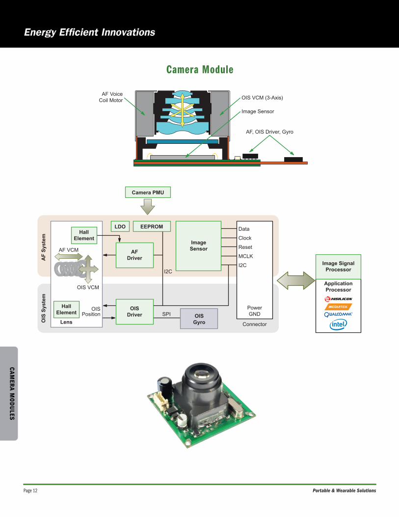
Camera Module
AF VoiceCoil Motor OIS VCM (3-Axis)
Image Sensor
AF, OIS Driver, Gyro
Data
I2C
SPI
ImageSensor
EEPROMLDO
AF
Sys
tem
OIS
Sys
tem
Camera PMU
AFDriver
OISDriver OIS
Gyro
Clock
Reset
MCLK
I2C
PowerGND
Connector
HallElement
Lens
OIS VCM
OISPosition
HallElement
AF VCM
Image SignalProcessor
ApplicationProcessor

Page 13ON Semiconductor
CAM
ERA
MO
DU
LES
CMOS Imaging Sensors
Features• Superior image quality with advanced pixel technology• Fast frame rates for action shots• Low power for battery operation• Great low light performance• Resolution choice including VGA to 4K (UHD)
The CMOS imaging sensor portfolio from ON Semiconductor provides options for all portable and wearable applications. Whether you’re building a new AR/VR headset, a 360 degree camera, a new set of imaging glasses, or simply a new wearable device that wants to see the world around it, ON Semiconductor has an Image sensor that can help you deliver an amazing end user experience.
Device Senor/SOCResolution
(MP)Optical Format Frame Rate
Pixel Size(mm)
Shutter Type1 CFA Temperature
MT9V115 SOC VGA 1/13” 30 fps 1.8 ERS Color -30 to +70°C
ASX340CS SOC VGA 1/4” 60 fps 5.6 ERS Color -30 to +70°C
ASX370CS SOC VGA 1/7” 30 fps 3 ERS Color -30 to +70°C
ARX3A0 Sensor VGA 1/10” Up to 360 fps 2.2 PGS Mono -30 to +70°C
MT9V024 Sensor WVGA 1/3” 60 fps 6 GS Color, Mono -40 to +105°C
MT9V034 Sensor WVGA 1/3” 60 fps 6 GS Color, Mono -30 to +70°C
AR0141CS Sensor 1.2 1/4” 1.2 45 fps, 720P 60 fps 3 ERS Color -30 to +85°C
AR0144CS Sensor 1 1/4” 60 fps 3 GS Color, Mono -40 to +85°C
AR0130CS Sensor 1.2 1/3” 1.2 45 fps, 720P 60 fps 3.8 ERS Color, Mono -30 to +70°C
AR0134CS Sensor 1.2 1/3” 1.2 54 fps, 720 60 fps 3.8 GS Color, Mono -30 to +70°C
AR0135CS Sensor 1.2 1/3” 1.2 60 fps, 720 60 fps 3.8 GS Color, Mono -30 to +70°C
MT9M114 SOC 1.3 1/6” 1.3 30 fps, VGA 75 fps 1.9 ERS Color -30 to +70°C
AR0230 Sensor 2.1 1/2.7” 60 fps 3 ERS Color -30 to +70°C
AR0237SR Sensor 2.1 1/2.7” 1080P 60 fps 3 ERS Color -30 to +85°C
AR0237IR Sensor 2.1 1/2.7” 1080P 60 fps 3 ERS RGB-IR -30 to +85°C
AR0238 Sensor 2.1 1/2.7” 1080P 60 fps 3 ERS Color -30 to +85°C
AR0239 Sensor 2.1 1/2.7” 1080P 90 fps 3 ERS Color -30 to +85°C
AR0261 Sensor 2.1 1/6” 1080p 60 fps 1.4 ERS Color -30 to +70°C
AS0260 SOC 2.1 1/6” 30 fps 1.4 ERS Color -30 to +70°C
AR0330 Sensor 3.5 1/3” 1080P 60 fps 2.2 ERS, GRR Color -30 to +70°C
AR0430 Sensor 4 1/3” 120 fps 2 ERS Color -30 to +70°C
AR0431 Sensor 4 1/3” 120 fps 2 ERS Color -30 to +85°C
AR0521 Sensor 5 1/2.5” 60 fps 2.2 ERS Color, Mono -30 to +85°C
AR0522 Sensor 5 1/2.5” 60 fps 2.2 ERS Color, Mono -30 to +85°C
AR1335 Sensor 13 1/3.2” 13 30 fps, 1080P 60 fps 1.1 ERS, GRR Color -30 to +70°C
AR1337 Sensor 13 1/3.2” 13 30 fps, 1080P 60 fps 1.1 ERS, GRR Color -30 to +70°C1. ERS = Electronic Rolling Shutter, GRR = Global Reset Release, GS = Global Shutter, PGS = Pseudo Global Shutter

Page 14 Portable & Wearable Solutions
CAM
ERA M
OD
ULES
Features• Integrated DSP software filter• Integrated Flash memory (40 KB)• Integrated OSC, LDO, and Hall amplifier• Digital Gyro I/F• 4-channel, 14-bit ADC; 3-channel, 8-bit DAC
LC898123F40 DSP-based Optical Image Stabilization (OIS) and Auto Focus (AF) controller/driver includes integrated Flash memory, analog circuits, H-bridge and constant current drivers. The integrated Flash enables fast wakeup and simplifies Host-side software implementation.
Optical Image Stabilization Drivers
Device TypeVDD Min
(V)VDD Max
(V)VM Min
(V)VM Max
(V)Driver(mA) CPU IF D/A A/D Package(s)
LC898123AXD Feedback 2.6 3.6 2.6 3.6 195/120 I2C 8-Bit 12-Bit WLCSP-35
LC898123F40 Feedback 2.6 3.3 2.6 3.3 200/150 I2C 8-Bit 14-Bit WLCSP-35
LC898123F40 Block Diagram
Flash(40 KBytes)
H-BridgeConst Current
for AFD-Gyro
IFI2CIF
OSC
DSP
DA
PositionSensor
AD PWM Logic
Control Logic
H-BridgeConst Current
for OIS

Page 15ON Semiconductor
CAM
ERA
MO
DU
LES
Features• Integrated equalizer circuit• Integrated EEPROM memory (128 byte)• Integrated OSC, LDO, and Hall amplifier• Integrated Constant Current Driver and Linear Compensation• 1-channel, 11-bit ADC; 2-channel, 8-bit DAC
LC898217XC/XH closed loop auto focus driver includes integrated driver, loop digital filter, and EEPROM. System implementation requires only a Hall sensor and by-pass condenser. LC898217XC/XH enables fast and accurate auto focusing, with low power consumption, from an extremely small footprint.
Closed Auto-Focus Drivers
Device TypeVDD Min
(V)VDD Max
(V)VM Min
(V)VM Max
(V)Driver(mA) CPU IF D/A A/D Package(s)
LC898214XD Feedback 2.6 3.6 — — 120 I2C 8-Bit 10-Bit WLCSP-8
LC898217XC/XH Feedback 2.6 3.3 — — 110 I2C 8-Bit 11-Bit WLCSP-10
LC898217XC/XH Block Diagram
OSC
DA
HallSensor
DA
AD Control LogicEqualizer
LDO I2C IF EEPROM
ConstantCurrentDriverHall
Amp

Page 16 Portable & Wearable Solutions
CAM
ERA M
OD
ULES
Motor Drivers for Camera ModulesFeatures
• Low power consumption • Low leakage • High precision control • PWM micro-stepping control on LV8414CS • Small PCB footprint
Brush DC Motor
CPU
Pop UpUnit
Stepper Motor Zoom
Voice Coil Motor Focus
Device MotorVM Max
(V)VCC Max
(V)Motor Current Max
(A)Step
Resolution Control Type PWM Constant
Current Protection Package
LV8414CS 2 x Stepper 6 6 0.4 1/64 I2C+Clock External Resistor TSD, UVLO WLCSP-32
LV8402GP Stepper / 2 x Brush DC 16 6 1.4 Half Parallel None TSD, UVLO VCT-24
LV8411GR 2 x Stepper / 4 x Brush DC 6 6 0.4 Half Parallel None TSD, UVLO VCT-24
LV8413GP Stepper / 2 x Brush DC 6 6 0.4 Half Parallel None TSD, UVLO VCT-16
LV8417CS Brush DC 12.6 6 1 - Parallel None TSD, UVLO WLCSP-9
LV8498CT Voice Coil - 5.5 0.15 1/1024 I2C Internal Resistor TSD, UVLO WLCSP-6

Page 17ON Semiconductor
CAM
ERA
MO
DU
LES
MIPI® Switching Devices
Application Processor
CSI-2RX
D-PHYRX
CLK_A+CLK_A-
Data0_A+Data0_A-
DataN_A+DataN_A-
CLK_B+CLK_B-
Data0_B+Data0_B-
DataN_B+DataN_B-
CLK+CLK-
Data0+Data0-
DataN+DataN-
Number of Data LanesMay Be 2, or 4DataN
CLK
D-PHY SwitchImage Sensor 1
Data
CLK
Data
D-PHYTX
CSI-2TX
Number of Data LanesMay Be 2, or 4DataN
CLKImage Sensor 2
Data
D-PHYTX
CSI-2TX
Features• Optimized bandwidth for high data rate transition• Low quiescent current consumption• WLCSP or UMLP package
Device Standard TypeVCC Max
(V)BW
(GHz)
Quiescent Current Max
(mA) Packages
FSA646A D-PHY & C-PHY 4-Lane 5.0 4.7 30 WLCSP-36
FSA646 D-PHY & C-PHY 4-Lane 5.0 4.1 30 WLCSP-36
FSA644 D-PHY 4-Lane 4.5 1.6 32 WLCSP-36
FSA642 D-PHY 2-Lane 4.3 1.1 1 UMLP-24
FSA660 C-PHY 1-Lane 5.0 5.0 30 UMLP-18

Page 18 Portable & Wearable Solutions
CAM
ERA M
OD
ULES
Camera Module PMICsFeatures
• Mid-size integration• 6-ouput PMIC ranging from 0.6 – 5.7 V and 0.3 – 1.2 A for camera and NFC power• Complements main PMU under minimum supervision• Reduced PCB routing and associated issues for required power management
• High performance• High efficiency dc-dc (96%) and low noise LDOs (<35 µVRMS)• Fully programmable through I2C for output voltages and sequencing
• Modular approach• 5 or 6 regulators for 2D/3D modules and back/front cameras
DeviceBuck(mA)
Boost(mA)
LDO(mA) Package
FAN53880 1 x 1200 1 x 1000 4 x 300 WLCSP-25
Page 19ON Semiconductor
POW
ER M
ANAG
EMEN
T
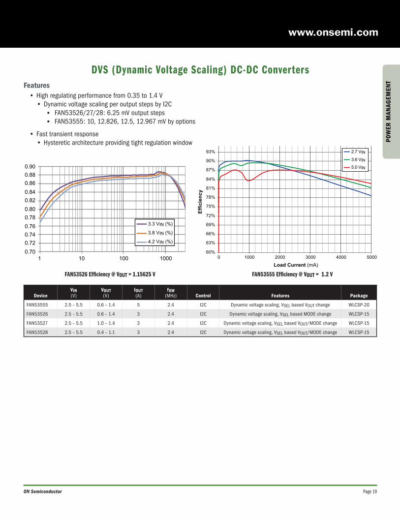
DVS (Dynamic Voltage Scaling) DC-DC ConvertersFeatures
• High regulating performance from 0.35 to 1.4 V • Dynamic voltage scaling per output steps by I2C
FAN53526/27/28: 6.25 mV output steps FAN53555: 10, 12.826, 12.5, 12.967 mV by options
• Fast transient response • Hysteretic architecture providing tight regulation window
DeviceVIN(V)
VOUT(V)
IOUT(A)
fSW(MHz) Control Features Package
FAN53555 2.5 – 5.5 0.6 – 1.4 5 2.4 I2C Dynamic voltage scaling, VSEL based VOUT change WLCSP-20
FAN53526 2.5 – 5.5 0.6 – 1.4 3 2.4 I2C Dynamic voltage scaling, VSEL based MODE change WLCSP-15
FAN53527 2.5 – 5.5 1.0 – 1.4 3 2.4 I2C Dynamic voltage scaling, VSEL based VOUT/MODE change WLCSP-15
FAN53528 2.5 – 5.5 0.4 – 1.1 3 2.4 I2C Dynamic voltage scaling, VSEL based VOUT/MODE change WLCSP-15
FAN53526 Efficiency @ VOUT = 1.15625 V FAN53555 Efficiency @ VOUT = 1.2 V
0.70
0.72
0.74
0.76
0.78
0.80
0.82
0.84
0.86
0.88
0.90
1 10 100 1000
3.3 VIN (%)
3.8 VIN (%)
4.2 VIN (%)
60%
63%
66%
69%
72%
75%
78%
81%
84%
87%
90%
93%
0 1000 2000 3000 4000 5000
Eff
icie
ncy
Load Current (mA)
2.7 VIN
3.6 VIN
5.0 VIN

Page 20 Portable & Wearable Solutions
POW
ER M
ANAG
EMEN
T
Peripheral DC-DC Converters
DeviceVIN(V)
VOUT(V)
IOUT(A)
fSW(MHz) Operating Mode Features Package(s)
NCP6323 2.5 – 5.5 0.6 – VIN 2 3 PWM, FB Resistor Power Good WDFN-8
NCP6324 2.7 – 5.5 0.6 – VIN 2 3PFM/PWM, FB
ResistorMode Selection (FPWM/PG) WDFN-8
FAN48611 2.5 - 4.8 5.25 0.35 2.5 PFM/PWM — WLCSP-9
FAN48610 2.5 – 4.8 3.3, 4.5, 5.0 1 2.5 PFM/PWM Pass-Through WLCSP-9
FAN48615/7/9 2.5 – 5.5 5.0, 5.25, 5.4 1 2.3 PWM Auto/Forced Pass-Through WLCSP-9
FAN48685 2.5 – 5.5 3.6/5.0/5.45 0.8 2.3 PWMAuto/Forced Pass-Through, Vout selection by
MODE0/1 pinWLCSP-9
FAN48630 2.35 - 5.53.15, 3.2, 3.33, 3.4, 3.49, 3.5, 3.7, 3.77, 4.5, 4.76, 5.0, 5.29
1.5 2.5 PWM/PFMAuto/Forced Bypass mode, Power Good, Vout
selection by VSEL pinWLCSP-15
FAN48630J 2.35 - 5.5 3.15/3.6 1.5 2.5 PWM/PFMAuto/Forced Bypass mode, Power Good, Vout
selection by VSEL pinWLCSP-15
FAN48632 2.35 - 5.5 3.3, 3.5, 3.71.5/2.0 pulsed
2.5 PWM/PFMAuto/Forced Bypass mode, Power Good, Vout
selection by VSEL pinWLCSP-15
FAN48623 2.5 - 5.5 3.0 – 5.0 2.5 2.5 PFM/PWM Bypass operation, VSEL based VOUT change WLCSP-16
FAN53600 2.3 – 5.5 2.8, 3.3 0.6 3 PFM/PWM Sync to external frequency, FPWM Mode WLCSP-6
FAN53610 2.3 – 5.5 2.9, 3.0, 3.3 1 3 PFM/PWM Sync to external frequency, FPWM Mode WLCSP-6
FAN53601 2.3 – 5.5 1.0, 1.05, 1.82 0.6 6 PFM/PWM Sync to external frequency, FPWM Mode WLCSP-6
FAN53611 2.3 – 5.51.1, 1.15,1.2, 1.233 1.3, 1.35, 1.8, 2.05
1 6 PFM/PWM Sync to external frequency, FPWM Mode WLCSP-6
FAN53602 2.3-5.5 1.233 1.2 6 PFM/PWM Sync to external frequency, FPWM Mode WLCSP-6
FAN53541 2.7-5.5 0.8 V to 90% of VIN 5 2.4 PFM/PWMSync to external frequency, Pin based MODE
change (AUTO/FPWM)WLCSP-20
FAN53741 2.3 – 5.5 0.6 – 5.5 1.3 2.5 PFM/PWM Programmable Current limit WLCSP-6
FAN49100 2.5 – 5.5 3.3, 3.6 2.5 1.8 PFM/PWM Automatic step-up/down, Pass-Through, FPWM WLCSP-20
FAN49103 2.5 – 5.5 2.8 – 4.0 (3.3, 3.4) 2.5 1.8 I2C Automatic step-up/down, Pass-Through, FPWM WLCSP-20
NCP1421 1.2 - 5.01.5 - 5.0 with external
resistors0.6 Up to 1.2
PFM/PWM, FB Resistor
— Micro8
NCP1422 1.0 - 5.01.5 - 5.0 with external
resistors0.8 Up to 1.2
PFM/PWM, FB Resistor
— DFN-10
NCP1423 0.8 - Vout1.8 - 3.3 with external
resistors0.4 Up to 0.6
PFM/PWM, FB Resistor
— Micro10
NCP6360 2.7 - 5.5 0.6 - 3.4 0.8 6 VCON Voltage Control Analog Input WLCSP-6

Page 21ON Semiconductor
POW
ER M
ANAG
EMEN
T
LDO Regulators
DeviceIO Typ(mA)
Iq Typ(mA)
Vin Min(V)
Vin Max(V)
VO(V)
PSRR(dB)
Noise(mVrms) Package(s)
NCP167 700 100 1.9 5.5 1.8, 2.8, 2.85, 3.0, 3.3, 3.5 85 8.5 CSP-4, XDFN-4
NCP133 500 80 0.8 5.5 0.9, 1.0, 1.05, 1.1, 1.15, 1.2, 1.25, 1.3, 1.5, 1.8, Adj 80 40 XDFN-6
NCP161 450 20 1.9 5.5 1.8, 2.5, 2.8, 2.85, 3.0, 3.3, 3.5, 4.5, 5.0, 5.14 90 10 CSP-4, XDFN-4
NCP114 300 50 1.7 5.51.0, 1.05, 1.1, 1.2, 1.25, 1.3, 1.5, 1.8, 2.1, 2.6, 2.8, 2.85, 3.0,
3.1, 3.3, 3.45, 3.575 60 UDFN-4, TSOP-5
NCP154 300/300 55 1.9 5.251.5/2.8, 1.8/2.7, 1.8/2.8, 1.8/2.9, 1.8/3.0, 2.8/2.7, 2.8/2.8, 3.0/1.8,
3.0/3.0, 3.1/3.1, 3.3/1.8, 3.3/2.8, 3.3/2.85, 3.3/3.0, 3.3/3.375 75 XDFN-8
NCP160 250 20 1.9 5.5 1.8, 2.5, 2.8, 2.85, 3.0, 3.3, 3.5, 4.5, 5.0, 5.14 90 10 CSP-4, XDFN-4
NCP163 250 120 2.2 5.5 1.8, 1.825, 1.9, 2.6, 2.75, 2.8, 2.85, 2.9, 2.925, 3.0, 3.3, 5.0 92 6.5 WLCSP-4, XDFN-4
NCP110 200 18 1.1 5.5 0.6, 0.8, 0.85, 1.05, 1.1,1.2, 1.8, 2.8 95 8.8 WLCSP-4, XDFN-4
NCP170 150 0.5 2.2 5.5 1.2, 1.5, 1.8, 2.5, 2.8, 3.0, 3.3 40 85 SOT-563, XDFN-4
NCP171 80 0.05 1.7 5.5 0.6, 0.75, 0.8, 1.0, 1.2, 1.6, 1.65, 1.7, 1.75, 1.8, 2.45, 2.5, 2.75, 2.8, 2.95, 3.0, 3.1, 3.25, 3.3 65 54 XDFN-4
0
25
50
75
100
125
1E+1 1E+3 1E+5 1E+7
PS
RR
(dB
)
ON Semiconductor LDO
Standard LDO
FREQUENCY (Hz)
Industry Leading High PSRR Performance3 mm x 3 mmTSOP-5
2 mm x 2 mmWDFN-6
1.2 mm x 1.2 mmXDFN-6
1.2 mm x 1.2 mmXDFN-4
1 mm x 1 mmXDFN-4
0.8 mm x 0.8 mmXDFN-4
0.65 mm x 0.65 mmCSP-4
1.2 mm x 0.8 mmCSP-6
<1.1 mm
TSOP-5SC-70-5
<1 mm
DFN
Hei
gh
t
<0.8 mm
WDFN
<0.6 mm
UDFN
<0.4 mm
XDFNCSP
Performance Leadership
Ultra-Low VIN of 1.1 VNCP110
Ultra-Low IQ of 50 nANCP171
PSRR of 92 dBNCP163
The LDO portfolio from ON Semiconductor provides solutions for all portable and wearable applications. Addressing the unique needs of these applications for reliable communication, low power, low quiescent current and long battery life plus small footprint, our LDOs offer ‘best in class’ performance, quality, and cost.

Page 22 Portable & Wearable Solutions
POW
ER M
ANAG
EMEN
T
Li-ion Battery Protection
Dual MOSFETs
Device Configuration PolarityVSSS Max
(V) VGSS Max
(V) IS (DC)
(A)
RSS(ON) @ VGS = 4.5 VMin/Typ/Max
(mΩ)
RSS(ON) @ VGS = 2.5 VMin/Typ/Max
(mΩ) Package(s)
ECH8693R Dual N-Channel 24 ±12 11 5.6/8.5/10.4 7.8/13.0/18.2 ECH-8
ECH8695R Dual N-Channel 24 ±12.5 11 5.6/7.0/9.1 7.5/9.5/13.3 ECH-8
ECH8697R Dual N-Channel 24 ±12 10 7.7/11.0/14.3 11.4/19.0/26.6 ECH-8
EFC4612R-S Dual N-Channel 24 ±12 6 24/39/45 33.5/58/72 EFCP
EFC4619R Dual N-Channel 24 ±12 6 13.5/19.8/23.0 18.5/27.0/35.0 EFCP
EFC4621R Dual N-Channel 24 ±12 9 10.8/15.5/18.0 14.9/23.0/30.0 EFCP
EFC4626R Dual N-Channel 24 ±12 5 29.2/37.5/46.2 42.6/54.0/72.4 EFCP
EMH2418R Dual N-Channel 24 ±12 8.5 9.1/13.0/16.9 13.8/23.0/32.2 EMH
EFC3C001NUZ Dual N-Channel 20 ±10 6 17.0/23.0/30.0 24.5/35.0/56.0 EFCP
EFC3J018NUZ Dual N-Channel 20 ±10 23 2.5/3.6/4.7 3.3/4.75/9.0 EFCP
EFC4627R Dual N-Channel 12 ±10 6 18.5/23.9/29.5 29.3/37.7/50.5 EFCP
EFC6604R Dual N-Channel 12 ±12 13 6.0/7.5/9.0 10.0/12.6/17.7 EFCP
EFC8811R Dual N-Channel 12 ±8 27 1.8/2.3/ 3.2 2.7/4.0/6.3 EFCP
NOTE: RSS(ON) = RDS(ON) x 2.
For Discharge For Charge
Dual MOSFET Configuration
BATT
D0VSS
C0
Controller
For Discharge For Charge
2-in-1 Configuration(Controller + Dual MOSFET Integrated Package)
VM
VDDBATT
D0CSVSS
C0
Controller
VM
VDD

Page 23ON Semiconductor
POW
ER M
ANAG
EMEN
T
Li-ion Battery Protection
Battery Protection Controllers with Integrated MOSFETs for One-Cell Batteries
Device
Adjustable Range
VSSS Max/ VGSS Max
(V)
RSS(ON) @ VGS = 4.5 VMin/Typ/Max
(mΩ)
RSS(ON) @ VGS = 3.1 VMin/Typ/Max
(mΩ) Features Package(s) VOV Range
(V) VUV Range
(V)
IOC/IOCH Range
(A)
LC05111CMT 4.0 to 4.5 2.2 to 2.7 2 to 8 24/±12 8.8/11.2/14.0 10.4/13/18.2 Auto Wake-up, 0 V Charge WDFN-6
LC05132C01NMT 4.0 to 4.5 2.2 to 2.8 2 to 8 24/±12 8.8/11.2/14.0 10.4/13/18.2 Reset Function ** WDFN-6
LC05732ARA 4.1 to 4.6 2.1 to 2.7 2 to 16 20/±10 3.8/4.7/5.6 4.4/5.4/6.9 Reset Function ** ECP-30
** Forced off of charge and discharge FET.
One-Cell Li-Ion Battery Protection Controllers
Device
Adjustable Range
Features Package(s) VOV Range
(V) VUV Range
(V)VOC Range
(mV) VOC2 Range
(mV)VSHRT Range
(mV)COCH Range
(mV)
LC05511XA 4.1 to 4.55 2.0 to 3.3 3 to 30 3 to 30 20 to 70 -30 to -3 Auto Wake-up, 0 V Charge WLCSP-6
LC05551XA 4.1 to 4.55 2.0 to 3.3 3 to 30 3 to 30 20 to 70 -30 to -3 Auto Wake-up, 0 V Charge , Reset Function ** WLCSP-8
LC06511DMX 4.1 to 4.55 2.0 to 3.3 3 to 70 3 to 70 50 to 150 -70 to -3 Auto Wake-up, 0 V Charge X2DFN-6
** Forced off of charge and discharge FET.

Page 24 Portable & Wearable Solutions
POW
ER M
ANAG
EMEN
T
Switching Battery ChargersFeatures
• Sized for micro USB connector (USB BC1.2) with 1.5 A, 1.6 A, 1.8 A, 2.5 A charging current
• Automatic input current limit adapts charging current to the maximum capability of the power source; proven charging time decrease by 10 minutes
• Integrated 28 V over voltage protection with unique negative voltage support
• Up to 1 A embedded boost USB OTG saves BOM cost• Automatically disconnects battery at end of charge, with
reconnect in few seconds in case of peak current activity (GSM for instance)
• Instant turn-on at cable insertion when battery is weak• Enable smart fast charging ports with input voltage capability up
to 16 V (NCP1855)
Device
Charging Current Max
(A)
Pre-Charge Current Max
(mA)
OTG Boost Current Max
(mA)
VCC Max (V)
OVP(V) I2C
Automatic Input Current
LimitingDual Path
Management
Protected USB PHY
Supply (mA)
Battery Temperature
Sensing Package
NCP1854 2.5 300 500 7 +28 400 kHz / 3.4 MHz Yes Yes (external) 50 JEITA Flip-Chip-25
NCP1855 2.5 300 500 16 +28 400 kHz / 3.4 MHz Yes Yes (external) 50 JEITA Flip-Chip-25
NCP1855 Charging Profile for 4.2 V, 2500 mAh Battery Pack, Input Source Limited to 1 A
Current &Voltage
Monitoring
DynamicPower Path
Management
300 mAPrecharge
AutomaticInput Current
Limiter
BatteryCharging
StateMachine
Battery
NT
C
15.5 V OperatingSwitching
Battery Charger
+28 VOvervoltageProtection
1000 mA5 V Boost
NCP1855
USBTransceiver
Supply
I2C400 kHz3.4 MHz
Page 25ON Semiconductor
POW
ER M
ANAG
EMEN
T
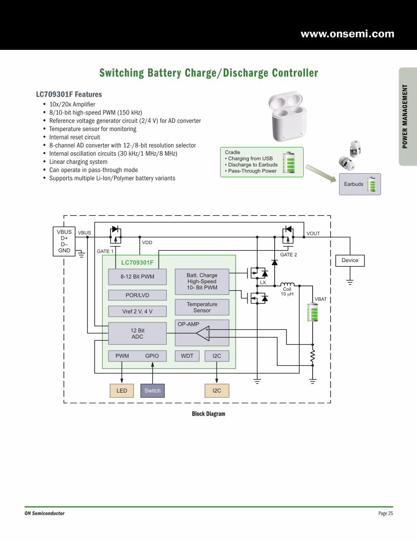
Switching Battery Charge/Discharge Controller
LC709301F Features • 10x/20x Amplifier • 8/10-bit high-speed PWM (150 kHz) • Reference voltage generator circuit (2/4 V) for AD converter • Temperature sensor for monitoring • Internal reset circuit • 8-channel AD converter with 12-/8-bit resolution selector • Internal oscillation circuits (30 kHz/1 MHz/8 MHz) • Linear charging system • Can operate in pass-through mode • Supports multiple Li-Ion/Polymer battery variants
Block Diagram
Cradle• Charging from USB• Discharge to Earbuds• Pass-Through Power
Earbuds
OP-AMP
WDT
POR/LVD
Vref 2 V, 4 VTemperature
Sensor
I2C
LC709301F
LED
I2CPWM GPIO
Switch
Batt. ChargeHigh-Speed10- Bit PWM
8-12 Bit PWM
GATE 1GATE 2
VBAT
VOUT
VDD
VBUS
LXCoil
10 μH
12 BitADC
VBUSD+D–
GND
Device

Page 26 Portable & Wearable Solutions
POW
ER M
ANAG
EMEN
T
LC709204F High Accuracy Battery Fuel GaugeFuel Gauge for 1 Cell Li+ with Low Power and with No Sense Resistor
Features• State of Health reporting• Accuracy of remaining capacity ±2.8% (0 ~ +50°C)• Ultra-low operating consumption current of 2 µA• Standby mode current (RAM retention) of 0.1 µA• No need for sense resistor for current detection
ON Semiconductor Solution (No Sense Resistor)
• No power loss• No heat generation
Conventional Display
Detailed Display ofRemaining Capacity
CorrectOperating Time
WithLC709204F
Standby Time120 h
Call Time75 min
77%
5 mΩ
SenseResistor
ConventionalSystem
MainBoard
FuelGauge
Battery
No Sense Resistor
ON SemiconductorSystem
MainBoard
FuelGauge
Battery
5 mΩ
SenseResistor
ConventionalSystem
MainBoard
FuelGauge
Battery
No Sense Resistor
ON SemiconductorSystem
MainBoard
FuelGauge
Battery

Page 27ON Semiconductor
POW
ER M
ANAG
EMEN
T
Depletion Mode Isolation Switches
Key Performance Characteristics• Passes ground and full swing audio signals with no power applied• Excellent isolation when power is applied, OIRR = -75 dB • Low power consumption when isolating, ICC = 80 µA typical• Low impedance ground path without power applied• Independent switch select lines enable system flexibility• Small chip scale package ideal for portable products and accessories
Depletion Mode Isolation Switches
1A
2A
1B
2B
#1S
#2SDepletion
GateControl
VCC
AudioSub-System
Processor
FSA553 FSA5512A
2B
DepletionGate
Control
1A
SW2SW11B
3 MΩ 3 MΩ
VCC
#1S #2S
VCC
VCC
Device DescriptionRON Typ
(Ω) THD+N TypIsolating VCC Range
(V)Conducting VSW Max
(V)Isolating VSW Max
(V) Package
FSA515 1-Channel Depletion Isolation Switch 0.7 -93 dB 2.5 - 5.5 -3.0 - 4.7 -3.0 - 4.7 WLCSP-4
FSA550 4-Channel Depletion Isolation Switch 0.8 -114 dB 1.6 - 3.0 ±2 0 - 1.4 WLCSP-12
FSA551 2-Channel Depletion Isolation Switch 0.4 -106 dB 1.5 - 3.0 -3.3 -3.3 WLCSP-9
FSA553 2-Channel Depletion Isolation Switch 0.4 -107 dB 1.5 - 3.0 ±1.5 ±1.5 WLCSP-9

Page 28 Portable & Wearable Solutions
POW
ER M
ANAG
EMEN
T
Power Distribution Load SwitchesFeatures
• Optimized for power sequence control and low power consumption by reducing current leakages
• Slew rate control to reduce inrush current• Low RON as low as 11 mΩ • Simplified layout reduces PCB footprint • WLCSP and DFN packages, as small as 0.76 mm x 0.76 mm
Load Switches
Device ChannelVIN Min
(V)VIN Max
(V)RDS(ON)
(mΩ)IOUT Max
(A)Discharge
Path RCB* Package
NCP433 Single 1 3.6 50 @ 1.8 V 1.5 Yes No WLCSP-4
NCP435 Single 1 3.6 29 @ 3.3 V 2 Yes No WLCSP-4
FPF1203 Single 1.2 5.5 55 @ 3.3 V 2.2 No No WLCSP-4
FPF1204 Single 1.2 5.5 55 @ 3.3 V 2.2 Yes No WLCSP-4
NCP451 Single 0.75 5.5 12 @ 3.6 V 3 No No WLCSP-6
NCP451A Single 0.75 5.5 12 @ 3.6 V 3 Yes No WLCSP-6
FPF1048 Single 1.5 5.5 23 @ 4.5 V 3 No Yes WLCSP-6
NCP340 Single 1.8 5.5 26 @ 3.0 V 3 No Yes UDFN-4
FPF1038 Single 1.2 5.5 21 @ 4.5 V 3.5 No No WLCSP-6
FPF1039 Single 1.2 5.5 21 @ 4.5 V 3.5 Yes No WLCSP-6
NCP459 Single 0.75 5.5 11 @ 3.3 V 4 Yes No WLCSP-8
FPF2411 Single 2.3 5.5 12 @ 3.8 V 6 No Yes WLCSP-12
FPF1320 DISO** 1.5 5.5 50 @ 3.3 V 1.5 No Yes WLCSP-6
FPF1321 DISO** 1.5 5.5 50 @ 3.3 V 1.5 Yes Yes WLCSP-6* Reverse Current Block. ** Dual Input Single Output.
A2
B2
A1
B1
FPF1204
Peripheral 1
GPIO 1
1.2 - 5.5 V
A2
B2
A1
B1
FPF1204
Peripheral 2
GPIO 2
ecoSWITCH™ Integrated Load Switch
Deviceron
(mΩ) I Max
(A) VI Min
(V) VI Max
(V) IQ
(mA) DischargeSlew Rate
(ms) Features Package(s)
NCP45524 18.0 6 0.5 13.5 - Adj - Power good DFN-8NCP45525 18.0 6 0.5 13.5 - Adj Adj - DFN-8NCP45560 2.4 24 0.5 13.5 - Adj Adj Power good; Fault DFN-12NCP45540 3.3 20 0.5 13.5 - Adj Adj Power good; Fault DFN-12NCP45541 3.3 20 0.5 13.5 - Adj Adj Power good DFN-12NCP45520 9.5 10.5 0.5 13.5 - Adj - Power good; Fault DFN-8NCP45521 9.5 10.5 0.5 13.5 - Adj Adj Fault DFN-8

Page 29ON Semiconductor
POW
ER M
ANAG
EMEN
T
Simple Load Switches
Device Polarity ConfigurationV(BR)DSS Min
(V) VGS Max
(V) ID Max
(A) RDS(ON) Max @ VGS = 4.5 V
(Ω) Package(s)
ECH8420 N-Channel Single 20 ±12 14 0.0068 ECH-8
MCH6421 N-Channel Single 20 ±12 5.5 0.038 MCPH-6
MCH6437 N-Channel Single 20 ±12 7 0.024 MCPH-6
MCH6448 N-Channel Single 20 ±9 8 0.022 MCPH-6
MCH6662 N-Channel Dual 20 ±10 2 0.16 MCPH-6
EMH2418R N-Channel Dual 24 ±12 8.5 0.0169 EMH-8
MCH6431 N-Channel Single 30 ±20 5 0.091 MCPH-6
NTLJD4116N N-Channel Dual 30 ±12 3.7 0.07 WDFN-6
NTLJS4114N N-Channel Single 30 ±12 6 0.035 WDFN-6
NTLUS4C12N N-Channel Single 30 ±20 9.1 0.015 UDFN-6
MCH3486 N-Channel Single 60 ±20 2 0.192 MCPH-3
MCH3333A P-Channel Single -30 ±10 2 0.215 MCPH-3
MCH6337 P-Channel Single -20 ±10 4.5 0.049 MCPH-6
NTLUD3A260PZ P-Channel Dual -20 ±8 1.7 0.2 UDFN-6
NTLUD3A50PZ P-Channel Dual -20 ±8 4.5 0.048 UDFN-6
NTLUS3A18PZ P-Channel Single -20 ±8 8.2 0.018 UDFN-6
ECH8308 P-Channel Single -12 ±10 10 0.013 ECH-8
MCH6336 P-Channel Single -12 ±10 5 0.043 MCPH-6
MCH6353 P-Channel Single -12 ±10 5.5 0.035 MCPH-6
NTLUS3C18PZ P-Channel Single -12 ±8 7 0.024 UDFN-6
PMU/Charging ICMOSFET
Vin USB
System
SecondaryCharging Pass
(Wireless)
Switching Charger – Step Down

Page 30 Portable & Wearable Solutions
POW
ER M
ANAG
EMEN
T
Optimized Schottky Diodes
Schottky Diodes in DSN-2 Package
DeviceIF (A)
VR (V)
VF @ Rated IF
(mV)
IR @ Rated VR
(mA)DSN2
PackageNSR01L30NX 0.1 30 460 0.3 0201 DSNNSR01F30NX 0.1 30 430 2 0201 DSNNSR02L30NX 0.2 30 530 0.4 0201 DSNNSR02F30NX 0.2 30 500 2 0201 DSNNSR05402NX 0.5 40 570 3 0201 DSNNSR05F20NX 0.5 20 390 15 0402 DSNNSR05F30NX 0.5 30 400 20 0402 DSNNSR05F40NX 0.5 40 420 15 0402 DSNNSR10404NX 1.0 40 500 10 0402 DSNNSR15304NX 1.5 30 530 20 0402 DSNNSR20204NX 2.0 20 540 15 0402 DSNNSR10F20NX 1.0 20 430 25 0502 DSNNSR10F30NX 1.0 30 450 30 0502 DSNNSR10F40NX 1.0 40 430 10 0502 DSNNSR15405NX 1.5 40 540 20 0502 DSNNSR20305NX 2.0 30 550 30 0502 DSNNSR20F30NX 2.0 30 425 40 0603 DSNNSR15406NX 1.5 40 510 20 0603 DSNNSR20206NX 2.0 20 450 40 0603 DSNNSR20306NX 2.0 30 440 40 0603 DSNNSR20406NX 2.0 40 520 35 0603 DSN
Schottky Diodes in X3DFN-2 Package
DeviceIF (A)
VR (V)
Max VF @ 10 mA
(mV)
Max IR @ 10 V (mA) Features
NSR01L30MX 100 30 460 0.2 Low LeakageNSR01F30MX 100 30 350 5 Low VFNSR02F30MX 200 30 290 15 Low VF
As wireless devices become smaller and thinner, more compact, energy efficient components are necessary. Power optimized Schottky diodes offer best in class thermal efficiency, and are considerably smaller than equivalent current handling devices. A lower forward voltage - compared to similar devices – also improves energy efficiency.
1.4
0.6
0.280.65
1.3
2.5
TOP VIEWTOP VIEW
DSN2 0502SOD-323 EP
SIDE VIEWSIDE VIEW
73%Smaller
57%Thinner
Dimensions in mm. Not to scale.
Package SizeDC-DC Boost Converter for LED Backlighting
DC-DC Buck Converter
CinVin
FB
SW
PWM
Rs
LED
VBAT
Cout
CinVin
AGnd
SW
PWM
Vout
FB
VBAT
Cout
0.1 0.2 0.3 0.4VF, Forward Voltage (V)
I F, F
orw
ard
Cur
rent
(A) DSN-2
SOD-323 EP
0.5 0.60.001
0.01
0.1
1
10
Energy Efficiency
00
22
44
66
88
1100
00 5500 110000 115500 220000
PPooww
eerr DD
iissssii
ppaattiioo
nn ((mm
WW))
OOuuttppuutt CCuurrrreenntt ((mmAA))
LLooww VVFF SScchhoottttkkyy LLooww IIRR SScchhoottttkkyy BBoooosstt OOppttiimmiizzeedd SScchhoottttkkyy
Schottky Diodes in Other Packages
DeviceIF (A)
VR (V)
VF @ Rated IF
(mV)
IR @ Rated VR
(mA) PackageNSR05T40XV2 0.5 40 530 3 SOD-523NSR05T30XV2 0.5 30 370 52 SOD-523NSR0520V2 0.5 20 410 75 SOD-523NSR0240V2 0.25 40 580 0.5 SOD-523NSR0340V2 0.25 40 470 1.5 SOD-523RB520S30 0.20 30 500 0.04 SOD-523RB521S30 0.20 30 400 20 SOD-523NSR10T20XV2 1.0 20 415 85 SOD-523NSR05T40P2 0.5 40 580 2 SOD-923NSR05T30P2 0.5 30 450 40 SOD-923NSR0620P2 0.5 20 480 9 SOD-923NSR0130P2 0.1 30 450 1 SOD-923NSR0230P2 0.2 30 400 20 SOD-923NSR0240P2 0.2 40 540 0.8 SOD-923NSR0340P2 0.2 40 520 4 SOD-923NSR0170P2 0.07 70 1.1 0.1 SOD-923NSR10T406MX 1.0 40 475 2 X2DFNW-2NSR05T404MX* 0.5 40 560 3 X2DFN-2NSR05T304MX 0.5 30 410 40 X2DFN-2SB2003M 2 30 450 70 SOT-363SS2003M 2 30 350 500 SOT-363SB3003CH 3 30 470 15 SOT-457SS3003CH 3 30 370 550 SOT-457
* Pending 2Q20.
Schottky Diodes in X4DFN 01005 Package
DeviceIF (A)
VR (V)
VF @ Rated IF (mV)
IR @ Rated VR (mA)
NSR01301MX4* 0.1 30 450 2NSR02301MX4* 0.2 30 420 25NSR05301MX4 0.5 30 640 25NSR05201MX4* 0.5 20 450 40
* Pending 2Q20.

Page 31ON Semiconductor
POW
ER M
ANAG
EMEN
T
Bipolar Transistors and Digital Transistors
Bipolar TransistorsON Semiconductor offers a wide portfolio of general purpose Bipolar Transistors. Below are the most common micro-packaged BJTs.
Digital TransistorsAs space becomes more constrained in wireless devices, integration becomes more desirable. Incorporating bias resistors into bipolar transistors performs this integration without degrading the performance of the transistor.
Low VCE(sat) BJTsON semiconductor is the leader in Low VCE(sat) BJTs with a portfolio that includes devices up to 6 A.
General Purpose Transistors
Device TechnologyVCE(max)
(V)IC(max)
(mA) Package
2SC5658M3 NPN 50 100 SOT-723
BC846BM3 NPN 65 100 SOT-723
2SA2029M3 PNP 50 100 SOT-723
BC856BM3 PNP 65 100 SOT-723
NST3904DP6 Dual NPN 40 200 SOT-963
NST3906DP6 Dual PNP 40 200 SOT-963
NST3946DP6 Comp NPN/PNP 40 200 SOT-963
NST847BDP6 Dual NPN 45 100 SOT-963
NST857BDP6 Dual PNP 45 100 SOT-963
NST847BPDP6 Comp NPN/PNP 45 100 SOT-963
NST3904F3 NPN 40 200 SOT-1123
NST3906F3 PNP 40 200 SOT-1123
NST847BF3 NPN 45 100 SOT-1123
NST857BF3 PNP 45 100 SOT-1123
Low VCE(sat) BJTs
Device PolarityVCE (V)
IC DC (A)
VCE(sat) 1 A, Beta 10,
Typ (mV)
Hfa @ 5 V, 100 mA,
Typ PackageNSS12100M3 PNP 12 1 280 250 SOT-723NSS12100XV6 PNP 12 1 280 250 SOT-563NSS12500UW3 PNP 12 5 55 250 WDFN-3NSS12501UW3 NPN 12 5 31 300 WDFN-3NSS12601CF8 NPN 12 6 30 300 ChipFETNSS20101J NPN 20 1 220 500 SC-89NSS20500UW3 PNP 20 5 60 250 WDFN-3NSS20501UW3 NPN 20 5 31 300 WDFN-3NSS20601CF8 NPN 20 6 31 300 ChipFETNSS35200CF8 PNP 35 2 79 253 ChipFETNSS40200UW6 PNP 40 2 100 250 WDFN-6NSS40500UW3 PNP 40 5 65 250 WDFN-3NSS40501UW3 NPN 40 5 38 300 WDFN-3NSS40600CF8 PNP 40 6 50 250 ChipFETNSS40601CF8 NPN 40 6 31 300 ChipFET
Digital TransistorsPart Body Number
R1(Ω)
R2(Ω) Package(s)
113E 1K 1K SOT-723, SOT-1123114E 10K 10K SOT-723, SOT-963, SOT-1123114T 10K None SOT-723, SOT-963, SOT-1123114Y 10K 47K SOT-723, SOT-963, SOT-1123115E 100K 100K SOT-723115T 100K None SOT-723, SOT-963, SOT-1123123E 2.2K 2.2K SOT-723, SOT-1123123J 2.2K 47K SOT-723, SOT-963, SOT-1123123T 2.2K None SOT-723, SOT-963, SOT-1123124E 22K 22K SOT-723, SOT-963, SOT-1123124X 22K 47K SOT-723, SOT-1123143E 4.7K 4.7K SOT-723, SOT-963, SOT-1123143T 4.7K None SOT-723, SOT-1123143Z 4.7K 47K SOT-723, SOT-963, SOT-1123144E 47K 47K SOT-723, SOT-963, SOT-1123144T 47K None SOT-723, SOT-1123144W 47K 22K SOT-723, SOT-963, SOT-1123
R1
R2
PIN 3COLLECTOR(OUTPUT)
PIN 2EMITTER(GROUND)
PIN 1BASE
(INPUT)
Page 32 Portable & Wearable Solutions
LCD
MO
DU
LES
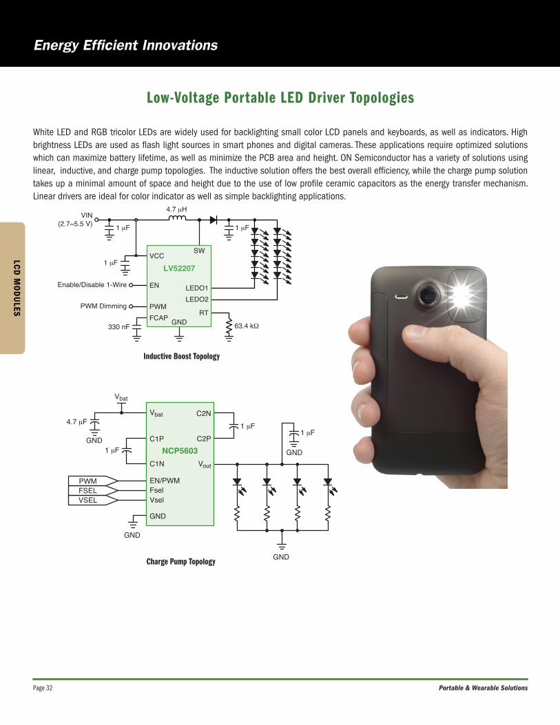
Low-Voltage Portable LED Driver Topologies
White LED and RGB tricolor LEDs are widely used for backlighting small color LCD panels and keyboards, as well as indicators. High brightness LEDs are used as flash light sources in smart phones and digital cameras. These applications require optimized solutions which can maximize battery lifetime, as well as minimize the PCB area and height. ON Semiconductor has a variety of solutions using linear, inductive, and charge pump topologies. The inductive solution offers the best overall efficiency, while the charge pump solution takes up a minimal amount of space and height due to the use of low profile ceramic capacitors as the energy transfer mechanism. Linear drivers are ideal for color indicator as well as simple backlighting applications.
Charge Pump Topology
1 F
GND
Vbat
4.7 F
GND
1 F
GND
GND
1 F
VSELFSELPWM
Vbat
C1P
C1N
EN/PWMFselVsel
GND
C2N
C2P
Vout
NCP5603
Inductive Boost Topology
330 nF
1 μF
1 μF
VIN(2.7~5.5 V) 1 μF
4.7 μH
63.4 kΩ
LV52207
SW
GNDFCAPRT
VCC
EN
PWM
Enable/Disable 1-Wire
PWM Dimming
LEDO1LEDO2
Page 33ON Semiconductor
LCD
MO
DU
LES
LED Drivers
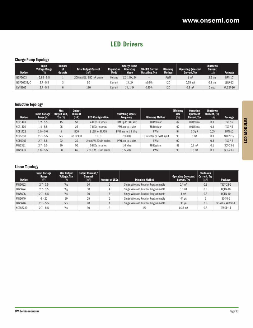
Charge Pump Topology
Device
Input Voltage Range
(V)
Number of
OutputsTotal Output Current
(mA)Regulation
Mode
Charge Pump Operating
ModeLED-LED Current
Matching, TypDimming Method
Operating Quiescent Current, Typ
Shutdown Current
(mA) Package
NCP5603 2.85 - 5.5 1 200 mA DC, 350 mA pulse Voltage 1X, 1.5X, 2X — PWM 1 mA 2.5 typ DFN-10
NCP5623B/C 2.7 - 5.5 3 90 Current 1X, 2X ±0.5% I2C 0.35 mA 0.8 typ LLGA-12
FAN5702 2.7 - 5.5 6 180 Current 1X, 1.5X 0.40% I2C 0.3 mA 2 max WLCSP-16
Inductive Topology
DeviceInput Voltage
Range (V)
Max Output Volt,
Typ (V)
Output Current
(mA) LED ConfigurationSwitching Mode/
Frequency Dimming Method
Efficiency Max (%)
Operating Quiescent
Current, Typ
Shutdown Current, Typ
(mA) Package
NCP1403 1.2 - 5.5 15 50 4 LEDs in series PFM up to 300 kHz FB Resistor 82 0.019 mA 0.3 TSOP-5NCP1406 1.4 - 5.5 25 25 7 LEDs in series PFM, up to 1 Mhz FB Resistor 92 0.015 mA 0.3 TSOP-5NCP1422 1.0 – 5.0 5 800 1 LED for FLASH PFM, up to 1.2 Mhz PWM 94 1.3 µA 0.05 DFN-10NCP5030 2.7 – 5.5 5.5 up to 900 1 LED 700 kHz FB Resistor or PWM Input 90 5 mA 0.3 WDFN-12NCP5007 2.7 - 5.5 22 30 2 to 6 WLEDs in series PFM, up to 1 Mhz PWM 90 — 0.3 TSOP-5FAN5331 2.7 - 5.5 20 50 5 LEDs in series 1.6 Mhz FB Resistor 89 0.7 mA 0.1 SOT-23-5FAN5333 1.8 – 5.5 30 65 2 to 8 WLEDs in series 1.5 MHz PWM 90 0.6 mA 0.1 SOT-23-5
Linear Topology
Device
Input Voltage Range
(V)
Max Output Voltage, Typ
(V)
Output Current / Channel
(mA) Number of LEDs Dimming MethodOperating Quiescent
Current, Typ
Shutdown Current, Typ
(mA) Package
FAN5622 2.7 - 5.5 VIN 30 2 Single Wire and Resistor Programmable 0.4 mA 0.3 TSOT-23-6FAN5624 2.7 - 5.5 VIN 30 4 Single Wire and Resistor Programmable 0.6 mA 0.3 UQFN-10FAN5626 2.7 – 5.5 VIN 30 6 Single Wire and Resistor Programmable 1 mA 0.3 UQFN-10FAN5640 6 – 20 20 25 2 Single Wire and Resistor Programmable 44 µA 5 SC-70-6FAN5646 2.7 – 5.5 5.5 20 1 Single Wire and Resistor Programmable 35 µA 0.3 SC-70-5, WLCSP-4NCP5623D 2.7 – 5.5 VIN 90 3 I2C 0.35 mA 0.8 TSSOP-14

Page 34 Portable & Wearable Solutions
LCD
MO
DU
LES
LCD Display Bias
The LV52133 and LV52134 generate user-programmable dual-out votages with a single inductor. Each device features short circuit protected output stages, small footprint, and ultra-low standby current.
Features• Dual-outputs with single-inductor architecture
• Adjustable output voltages via I2C
• Short Circuit Protection
Device Input Voltage Range Default Output Voltage Output Voltage Setting Range Output Current Standby Current Package
LV52133A0XALV52134A0XA
2.5 to 5.5 V
VOUT1 = +5.0 VVOUT2 = -5.0 V VOUT1: +4.1 to +5.7 V
VOUT2 : -4. V to -5.7 V(100 mV step)
200 mA (VOUT1);100 mA (VOUT2)
0.3 mA WLP-15JLV52133A5XALV52134A5XA
VOUT1 = +5.5 VVOUT2 = -5.5 V
2.2 μF
4.7 μH 2.5 to 5.5 VVbat
4.7 μF
4.7 μF
-5 V
+5 V4.7 μF
4.7 μF
LX
PGND
CP
CN
SGND
SDA
SCL
VIN
VBST
VOUT1
VOUT2
EN1
EN2
NOTE: LV52133 and LV52134 differ with respect to I2C control address.

Page 35ON Semiconductor
LCD
MO
DU
LES
LC898302A LC898301
Device Description Package
LC898302A Haptic Driver for LRA and ERM WLCSP-6
Device Description Package
LC898301XA Haptic Driver for LRA WLCSP-8
LC898301AXA Haptic Driver for LRA with Immersion System WLCSP-8
Block Diagram
Block Diagram
Unique Features• Drive LRAs with automatic tuning and breaking
• Drive ERM; drive voltage controlled via PWM
Other Features• Supply voltage = +2.7 to +4.5 V
• Iout max = 200 mA
• Bridge RDS(on) = 2 x 2 Ω (4 x 2 Ω MOSFETs embedded)
• Low standby current
Benefits• High efficiency
• Easy handling (no adjustment for any LRA)
• Strong vibration
Unique Features• Automatically adjust driving frequency (ON Semiconductor
patent)
• Minimized start-up and brake period (Quick stop)
• Automatically stop braking to avert counter vibration
Other Features• Supply voltage = +3.0 to +5.5 V
• Iout max = 200 mA
• Bridge RDS(on) = 2 x 2 Ω (4 x 2 Ω MOSFETs embedded)
• No peripheral component required (only 0.1 µF cap)
• Low power consumption
Benefits• High efficiency
• Easy handling (no adjust-ment for any LRA)
• Strong vibration
• Fault-detection
• Battery direct supply
• Fully configurable through I2C
Haptic Drivers
The LC898302A is a haptic driver able to drive LRA and ERM. The drive
frequency is automatically adjusted to the resonance frequency of the
linear vibrator without external components.
The LC898301 is an extended supply range version of the LC898300
LRA driver, compatible with cellular battery voltage. The architecture
chosen enables strong vibration in minimal board space. Moreover, the
LC898301 exhibits superior vibration performance.
H-Bridge withPower Control
Drive SignalGenerator
RegisterSetting OSC
LDO
SCL<I2C IF>
EN
DVDD (1.8 V)
VDD (3.0-5.5 V)
OUT1
OUT2
LinearVibrator
SDA
VSSRSTB
H-BridgeDriver
Drive SignalGenerator
TSD
PORLDO
OSC
PWM
VDD (2.7 to 4.5 V)
OUT1
OUT2
LRAERM
MODE
VSS

Page 36 Portable & Wearable Solutions
PROTEC
TION
Protection Solutions
External Interface
Camera/Display Lines
Single Ended Data
Audio
Other Lines
Charging
USB 3.xUSB 4.0
USB 2.0
SDR50SDR104
SIM
Speaker
Lo
w S
pee
d S
ing
le E
nd
ed D
ata/
Au
dio
Hig
h S
pee
d D
iffe
ren
tial
Dat
a
Headphone
Microphone
General PurposeESD Protection
USB VbusBattery Contacts
< 0.3 pF, industry leading insertion loss
Low clamping voltage
Unidirectional and Bidirectional
Singles and space efficient arrays
Smallest footprint in the industry
•
•
•
•
•
> 30 dB CM Attenuation
Support for up to 8 Gbps
Lowest clamping voltage in its class
1, 2, 3 pairs available
•
•
•
•
Industry leading power density
> 10 A Surge capable in 0201 form factor
Smallest footprint in the industry
Singles and arrays
•
•
•
•
> 40 dB Attenuation at antenna frequency
Low clamping voltage
Extremely low cross-talk
Small form factor
•
•
•
•
Ipp > 180 A (8x20 µs)
Superior clamping performance
4.8 V to 18 V VRWM options
Unidirectional and Bidirectional
•
•
•
•
eFuses
Power Switches
•
•
High Surge Protection
Current/Voltage Protection
ESD Protection
EMI Filter
ESD Protection
EMI Filter

Page 37ON Semiconductor
PRO
TEC
TIO
N
Audio Filtering for HiFi
EMI7112 Features• >40 dB @ 750 MHz to 2.4 GHz • Cross-talk < –65 dB, THD+N < 0.006%• HiFi quality capable
EMI7112 THD + N EMI7112 Crosstalk with 1 Vpp Input Voltage
-115
-110
-105
-100
-95
-90
-85
-80
20 200 2000 20000
TH
D+
N, d
B
Frequency, Hz
EMI7112 Ch1 1 Vrms
EMI7112 Ch2 1 Vrms
-135
-125
-115
-105
-95
-85
-75
-65
20 200 2000 20000
Cro
ssta
lk, B
Frequency, Hz
SMA #7 B/A 1 Vpp
SMA #8 B/A 1 Vpp
SMA #9 B/A 1 Vpp
SMA #10 B/A 1 Vpp
SMA #11 B/A 1 Vpp
SMA #12 B/A 1 Vpp
Common Mode Filters for High Speed Interfaces
Function Filter CM Noise Signal Integrity Protect ChipsetDevice Series
Attenuation > 25 dB range RF Receivers
Maximum Data Rate Interfaces Supported
Vc @ 8 kV (TLP)
Minimum Chipset Geometry
EMI813x 700 MHz – 1.1 GHz LTE, GSM, 4 Gb/s USB2.0; MHL1-2; HDMI1.3/4; MIPI CSI-2 11.6 V 14 nm
EMI814x 1.3 GHz – 3 .0 GHz LTE, WCDMA, WiFi, GPS 8 Gb/s USB3.0; MIPI CSI-3; MHL3.0; HDMI2.0 11.6 V 14 nm
-50
-45
-40
-35
-30
-25
-20
-15
-10
-5
0
100.00 1000.00
SC
C21
, dB
Frequency, MHz
Key Antenna Frequency Windows
EMI813x
EMI814xON SemiconductorCompetitors
Deepest Attenuation =
Improved Antenna Reception

Page 38 Portable & Wearable Solutions
PROTEC
TION
ESD Protection for High Speed Data LinesIndustry leading insertion loss with excellent clamping performance
Device PolarityVRWM
(V)
8 x 20 ms Surge
Capacitance(pF)
Capacitance Max(pF) No of Lines Package
IPP Min (A)
VClamp @ IPP (V)
ESD8011 Bidirectional 5.5 3.6 8.7 0.1 0.2 1 X3DFN-2
ESD8351 Unidirectional 3.3 5 8.2 0.37 0.55 1 X3DFN-2
ESD8111P Bidirectional 3.3 7.1 8 0.2 0.4 1 X4DFN-2
ESD7331 Bidirectional 3.3 2.5 7.5 0.4 0.75 1 X3DFN-2
ESD7501 Bidirectional 5 2 9.9 0.45 0.75 1 X3DFN-2
ESD9L5.0 Unidirectional 5 1 9 0.5 0.9 1 SOD-923
ESD9L3.3 Unidirectional 3.3 1 9.8 0.5 0.9 1 SOD-923
ESDL3552 Bidirectional 5 2 14 0.25 0.3 2 X4DFN-3
ESD8704 Unidirectional 3.3 7.5 6.7 0.37 0.5 4 UDFN-10
ESD8104 Unidirectional 3.3 3.5 8.1 0.3 0.37 4 UDFN-10
ESD8116 Unidirectional 3.3 3.5 8 0.3 0.35 6 UDFN-8
ESD8118 Unidirectional 3.3 3.5 8.1 0.3 0.35 8 UDFN-10
ESD8008 Unidirectional 3.3 5 5 0.3 0.35 8 UDFN-14
ESD7181 Bidirectional 18.5 1 32 0.3 0.5 1 X3DFN-2
ESD7241 Bidirectional 24 2.5 37 0.55 1 1 X2DFN-2
ESDL2011 Bidirectional 1 4.3 4.6 0.15 0.2 1 X4DFN-2
ESDL2031 Bidirectional 4 8 5.5 0.37 0.55 1 X4DFN-2
ESDL1531 Bidirectional 3.3 7.5 8.6 0.15 0.3 1 X4DFN-2
LVPT Arrays — 100 ns TLP
0
2
4
6
8
10
12
14
16
18
0 2 4 6 8 10 12 14 16
Cur
rent
(A
)
Clamping Voltage (V)
2kV
4kV
6kV
8kV
ESD8104/16/18Lowest Clamping Voltage
Competition
IEC
61000-4-2 Eq
uivalen
t Level
Applications• USB 2.0/3.x/4.0• Thunderbolt™ 2.0/3.0• HDMI® 1.4/2.x• MHL® 3/superMHL• MIPI® D/M/C PHYs• NFC™ & Wi-Fi® Antenna Protection• DisplayPort® 1.4/2.0
SCR Arrays — 100 ns TLP
0
2
4
6
8
10
12
14
16
18
0 2 4 6 8 10 12 14 16
Cur
rent
(A
)
Clamping Voltage (V)
2kV
4kV
6kV
8kV
ESD8704Lowest Clamping Voltate
Fastest Response
Competition
IEC
61000-4-2 Eq
uivalen
t Level

Page 39ON Semiconductor
PRO
TEC
TIO
N
ESD Protection Featuring X4DFN — Smallest Package in the IndustryIdeal ESD protection solutions for space constrained applications
Industry leading X4DFN package offers• Six side silicon encapsulation • Best ESD protection performance in its class• Increased reliability
• Protective mechanical layer no chipping• Electrical insulation prevents short circuit conditions• Moisture barrier no corrosion• Lower reflectivity friendly to automated inspection• Light barrier reduces leakage caused by light sensitivity
High Speed Data Protection — 8 x 20 ms Surge Comparison 5 V GPIO Protection — 8 x 20 ms Surge Comparison
0.3 mm 0.24 mm
0.44 mm0.6 mm
44%Area
Improvement
0201 01005
0
2
4
6
8
10
12
0 1 2 3 4 5 6 7 8 9
VC
@ Ip
k (V
)
Ipk (A)
ESDL1531Competition
0
2
4
6
8
10
12
14
0 1 2 3 4 5 6 7 8 9 10 11 12 13
VC
@ Ip
k (V
)
Ipk (A)
ESDM1051
Competition
X4DFN USB Type-C Evaluation Board
Device
ESDContact/Air
(kV)VRWM
(V)Cj Typ (pF)
Cj Max (pF)
8 x 20 ms Surge
RDYN TLP(Ω) SCR
IPP Typ (A)
VClamp Typ (V)
IPP Min (A)
VClamp Max (V)
ESDL1531 25/25 3.3 0.15 0.3 7.5 8.6 6.5 11.5 0.46 Yes
ESDM1131 16/16 3.3 4 5.5 4.25 6.2 3.5 6.6 0.125 No
ESDM1031* 30/30 3.3 36 40 13.5 9.6 9.5 10.5 0.21 No
ESDM1032* 30/30 3.3 21 23.5 12.5 8.4 11 10 0.11 No
ESDM1051 30/30 5.5 21 23.5 12 8.5 11 10 0.11 No
ESDM1121* 15/15 12 15 20 4 19.5 3 22 0.59 No
* Pending 2Q20.

Page 40 Portable & Wearable Solutions
PROTEC
TION
ESD Protection for GPIOSmall form factor solutions with lowest clamping voltage in class
Applications• SIM Card protection• SD Card protection• Biometrics/finger print sensor• Audio In/Out• USB Type C configuration channel• Manufacturing test points
SD BiometricsSIM MicSpeaker/Headphones
CC/SBU TestPoints
Device PolarityVRWM
(V)
8 x 20 ms Surge Capacitance Max(pF) No of Lines Package
IPP Min (A)
VClamp @ IPP (V)
ESDM3031 Bidirectional 3.3 11 8.4 20 1 X3DFN-2
ESDM3051 Bidirectional 5 10 8.7 21 1 X3DFN-2
ESDM3551 Bidirectional 5.5 9.9 8.8 21 1 X3DFN-2
ESDM2032* Bidirectional 3.3 14 5.5 20 1 X4DFN-2
ESDM3032 Bidirectional 3.3 7.5 8.5 10 1 X3DFN-2
ESD5581 Bidirectional 5 6 10.3 10 1 X3DFN-2
ESD5111P Bidirectional 3.3 4 5.8 5.5 1 DSN-2
ESDM1131 Bidirectional 3.3 3.9 5.7 5 1 X4DFN-2
ESD5102 Bidirectional 3.3 — — 5.5 2 DSN-3
ESD5004 Bidirectional 3.3 3 6.8 5 4 X3DFN-4
ESDM1031* Bidirectional 3.3 9.5 10.5 40 1 X4DFN-2
ESDM1032* Bidirectional 3.3 11 10 23.5 1 X4DFN-2
ESDM1051 Bidirectional 5.5 11 10 23.5 1 X4DFN-2
ESDM1121* Bidirectional 12 3 19.5 20 1 X4DFN-2
* Pending 2Q20.
100 ns TLP I-V CurveClamping Voltage vs Peak Pulse Current – tp=8/20 ms
8
7
6
5
4
3
2
1
0
0 1 2 3 4 5 6 7 8 9IPK (A)
VC
@ I P
K (
V)
10 11 12 13 14 15 16 17 180
2
4
6
8
10
12
14
18
16
20
0
1
2
3
4
5
6
7
9
8
10
0 2 4 6 8 10 12 14 16 18 20
Cur
rent
(A
)
VIE
C E
q (
kV)
Clamping Voltage (V)
ESDM1051ESDM2032
0.3 mm
0.6 mm
0.24 mm
Lowest DynamicResistance in its Class
RDYN = 0.125 Ω
0.44 mm

Page 41ON Semiconductor
PRO
TEC
TIO
N
Surge ProtectionHigh performance, space efficient solutions
Applications• VBUS line • Battery line• Audio In/Out• USB Type C Configuration Channel• LCD power line• RF Power Amplifier power line
Device PolarityVRWM
(V)
8 x 20 ms Surge
PackageIPP Min
(A)VClamp @ IPP
(V)
NSPM0061 Unidirectional 6.3 70 11.3 UDFN-2
NSPM0101 Unidirectional 10 60 18.2 UDFN-2
NSPM8151 Unidirectional 15 100 24.5 UDFN-6
NSPM8181 Unidirectional 18 119 31.5 UDFN-6
NSPU3051 Unidirectional 5.5 36 7.5 SOD-882
NSPU3061 Unidirectional 6.3 30 7.3 SOD-882
NSPM3031 Bidirectional 3.3 45 7 SOD-882
NSPM3042 Bidirectional 4.8 43 7.4 SOD-882
NSPU5132 Unidirectional 13.5 200 22 UDFN-6
NSPU5221 Unidirectional 22 120 34 UDFN-6
NSPM2052 Unidirectional 5 120 8 UDFN-2
NSPM1042 Bidirectional 4.8 200 8.8 UDFN-2
VBUS VBAT MicSpeaker CC/SBU
8 x 20 ms Surge Performance – VBAT Protection
0
1
2
3
4
5
6
7
8
9
0 20 40 60 80 100 120 140
VC
@ Ip
k (V
)
Ipk (A)
NSPM2052
1.0 mm
1.6 mm
0
1
2
3
4
5
6
7
8
9
0 5 10 15 20 25 25 30 35 40 45
NSPM3042
VC
@ Ip
k (V
)
Ipk (A)
0.6 mm
1.0 mm

Page 42 Portable & Wearable Solutions
PROTEC
TION
Power ProtectionSurge and Over-Voltage Protection Switches
Over Current Protection Switches
Features• Optimized for Input Power Stage with USB-C• 100 V Surge Capable Integrated TVS• Low RON for Low Power Loss• Fast Over Voltage Response Time• Design Flexibility with Adjustable/Selectable OVP• Reverse Current Block• Compact Packages, WLCSP and DFN
Features• Optimized for 5V USB-OTG and VCONN with USB-C• Fast Over Current Response Time• Design Flexibility with Adjustable Current Limit Set• True Reverse Current Block• Compact Packages, WLCSP and DFN• UL Certified
HV BatteryCharger
Processor
1 μF
TravelAdapter
Legacy USB/USB Type-CConnector
1 μF
RPU
R1
R2
FPF2281
IN OUT
#ACOKOVLO
#EN GND
VIO
COUT
5 VBoost
AP
Battery
CIN
USBConnector
VIO
OTGDevice
FPF2595
ON
Vin
OC_FLAGB
Vout
ISET GND
* Default but Adjustable w/ external R. ** Selectable w/ Logic Pins. *** Single Input Dual Output. ^ Dual Input Single Output. ^^ By Option.
Over Voltage Protection Switches
Device ChannelVIN Min
(V)VIN Max
(V)OVP (V)
RON (mΩ)
IOUT Max (A) Integrated TVS Discharge Path Package
FPF2280 Single 2.5 28 6.8* 30 @ 5.0 V 4.5 Yes No WLCSP-12
FPF2281 Single 2.5 28 14* 30 @ 5.0 V 4.5 Yes No WLCSP-12
FPF2290 Single 2.5 28 SEL** 30 @ 5.0 V 4.5 Yes No WLCSP-12
FPF2498 Single 3.5 28 6.5 80 @ 5.0 V 1.75 No No WLCSP-6
NCP398 Single 2.9 28 5.65 190 @ 5.0 V 0.8 No Yes WLCSP-4
FPF3042 DISO^ 4 18 14 70 @ 5.0 V 2.7 No No WLCSP-16
NCP367 Single 1.2 28 OPN^^ 50 @ 3.5 V 3.4 No No DFN-8
* Reverse Current Block. ** Single Input Dual Output. *** By Option.
Over Current Protection Switches
Device ChannelVIN Min
(V)VIN Max
(V)RON (mΩ)
ILIM Range (A) OVP RCB* Package
FPF2195 Single 1.8 5.5 55 @ 3.3 V 0.1 ~ 1.5 No Yes WLCSP-6
FPF2495 Single 2.5 5.5 70 @ 5.0 V 0.05 ~ 2.0 Yes Yes WLCSP-9
FPF2496 Single 3.5 5.5 70 @ 5.0 V 0.1 ~ 2.5 Yes Yes WLCSP-9
FPF2595 Single 2.5 5.5 35 @ 5.0 V 0.1 ~ 3.5 Yes Yes WLCSP-12
FPF2895C Single 4 22 27 @ 5.0 V 0.5 ~ 5.0 Yes Yes WLCSP-24
NCP380 Single 2.5 5.5 55 @ 5.0 V 0.5 ~ 2.1 No Yes UDFN-6
NCP382 SIDO** 2.5 5.5 80 @ 5.0 V Fixed*** No Yes DFN-8
NCP383 SIDO** 2.7 5.5 45 @ 5.0 V 0.5 ~ 2.8 No Yes UDFN-10

Page 43ON Semiconductor
PRO
TEC
TIO
N
Enable/Fault
ChargePump
dv/dtControl
CurrentLimit
SASDisable
CurrentMonitor
ThermalShutdown
UVLO
VoltageClamp
VOUT
VIN
ILIM
dv/dt
GND
SASIN
ISENSE
EN/FLT
VINT
EN/FLT
VINT
VINT
SAS
VBUS
VBUSVINT
dv/dt
VBUS
VBUS
ILIM RLIM
I SE
NS
EG
ND
GN
D
eFuses (Electronic Fuses)5 – 12 V Power Bus Overcurrent and Hot Plug Protection
• Low RDS(ON), high operating and trip currents (IOP, ITRIP) • Overvoltage protection • Precise ITRIP control • Slew rate control • Thermal shut-down • EN pin for synchronizing multiple eFuses • Reverse current blocking to protect downstream data • Fast-role swap capability for USB Type-C • Surge protection per IEC 61000-4-5
• Outperforms poly-fuses: Tighter spec tolerances Lower resistance Shorter trip-time Superior repeatability
• High efficiency with high current capability • eFuses in parallel achieve practically any desired level of IOP and ITRIP
Features
Application Diagram Typical Block Diagram
DeviceNominal Voltage
(V)Input Voltage
(V)
Output Clamping Voltage
(V)
ContinuousCurrent
(A) Trip CurrentRDS(ON)
(mΩ) Auto-Retry Latching Package
NIS5021 12 -0.3 to 20 14 12 Adjustable 14 3 3 WDFN-10
NIS5020 12 -0.3 to 20 14 10 Adjustable 14 3 3 WDFN-10
NIS5820 12 -0.3 to 20 14 8 Adjustable 24 3 3 WDFN-10
NIS5132 12 -0.6 to 18 15 4.2 Adjustable 44 3 3 DFN-10
NIS5232 12 -0.6 to 18 15 4.2 Adjustable 44 3 DFN-10
NIS5135 5 -0.6 to 18 6.65 3.6 Adjustable 68 3 3 DFN-10
NIS6452 5 -0.3 to 14 7.0 3 Adjustable 60 3 3 WQFN-12
NIS6350 5 -0.3 to 10 6.1/6.9 3 Adjustable 70 3 3 WDFN-10
NIS6150 5 -0.3 to 10 6.1/6.9 1 Adjustable 190 3 3 WDFN-10
NIS6432 3.3 -0.3 to 14 4.4 3 Adjustable 60 3 3 WQFN-12

Page 44 Portable & Wearable Solutions
INTER
FACE &
MEM
OR
Y
EEPROMs for Configuration and Calibration
EasyPRO™ is a user-friendly, portable programming tool for ON Semiconductor
serial EEPROMs (I2C, SPI, Microwire)
Features• Broad density range: 1 kb to 2 Mb• Wide operating Vcc range: 1.7 V to 5.5 V• High endurance: 1 million program/erase cycles• Wide temperature range: industrial and extended
EEPROMsData
Transmission Standard Density Organization*
VCC Min(V)
VCC Max(V)
fCLK Max(MHz) Package(s)
I2C
1 Mb 128k x 8
1.7, 1.8 5.5 0.4, 1 US8, SOIC-8, TSSOP-8, UDFN-8, TSOT23-5, WLCSP-4, WLCSP-5, WLCSP-8
512 kb 64k x 8256 kb 32k x 8128 kb 16k x 864 kb 8k x 8
32 kb 4k x 8
16 kb 2k x 88 kb 1k x 84 kb 512 x 82 kb 256 x 8
SPI
2 Mb 256k x 8
1.7, 1.8 5.5 10, 20 SOIC-8, TSSOP-8, UDFN-8
1 Mb 128k x 8512 kb 64k x 8256 kb 32k x 8128 kb 16k x 864 kb 8k x 832 kb 4k x 816 kb 2k x 88 kb 1k x 84 kb 512 x 82 kb 256 x 81 kb 128 x 8
Microwire
16 kb 2k x 8 / 1k x 16
1.65, 1.8 5.5 2, 3, 4 SOIC-8, TSSOP-8, UDFN-8
16 kb 2k x 8 / 1k x 168 kb 1k x 8 / 512 x 168 kb 1k x 8 / 512 x 164 kb 512 x 8 / 256 x 162 kb 256 x 8 / 128 x 161 kb 128 x 8 / 64 x 161 kb 128 x 8 / 64 x 16
* Organization for Microwire devices is selectable.

Page 45ON Semiconductor
INTE
RFA
CE
& M
EMO
RY
RF/NFC EEPROM
Tablet/Phone
RFReader/Writer
Motor Trimfrom EEPROM
TV Trimfrom EEPROM
AdjustableCurrent
Regulator
LED
MCU
LED TV
N24RF64EEPROM
I2C Bus
Trim parameters,diagnostic data,
remote maintenance
Sample Application
DeviceMemory Density
(kb)Energy Harvesting
Output Temperature Range Package(s)N24RF64E 64 Yes -40 to +105°C SOIC-8, TSSOP-8
N24RF64 64 No -40 to +105°C SOIC-8, TSSOP-8
N24RF16E 16 Yes -40 to +105°C SOIC-8, TSSOP-8
N24RF16 16 No -40 to +105°C SOIC-8, TSSOP-8
N24RF04E 4 Yes -40 to +105°C SOIC-8, TSSOP-8
N24RF04 4 No -40 to +105°C SOIC-8, TSSOP-8
Features• RF/NFC interface for contactless transmission of data up to 150 cm• ISO 15693 / ISO 18000-3 Mode 1 Compliant RF/NFC at 13.56 MHz• 2,000,000 Program / Erase Cycles • 200 year data retention• 64-bit Unique Identifier (UID) • Multiple 32-bit passwords and Lock Feature• I2C Interface
• 4 selectable slave addresses using pins A0 ad A1• 1 MHz bus speeds
• Energy harvesting output pin; able to power small peripheral or MCU
RF EEPROMs
MCU
Batteries Not Required
VccVcc
SCL
SDA
Vout
VssVss
N24RFxxERF/NFC

Page 46 Portable & Wearable Solutions
INTER
FACE &
MEM
OR
Y
Serial NOR Flash Memory
Features• SPI interface• Supply voltage 1.65 to 1.95 V• Minimum erase size (4 KB/64 KB)• Fast write perfomance (Sector Erase/Page Program)• Low standby current; support for deep standby mode
Device DensityPower Supply
(V) Erase SizeSector Erase Time
(ms)Page Program Time
(ms)Read/Write/Standby Current, Typ
(mA) Package
LE25S20 2 Mb 1.65 - 1.95 4 KB/64 KB/2 Mb 80 3.0 6.0/15.0/0.010 WLCSP-8
LE25S81 8 Mb 1.65 - 1.95 4 KB/64 KB/8 Mb 80 0.3 6.0/18.0/0.010 WLCSP-8
LE25S161 16 Mb 1.65 - 1.95 4 KB/64 KB/16 Mb 15 0.4 6.0/6.5/0.009 UDFN-8, WLCSP-8
LCD Panel
Touch Rx
SPI
TouchData
ImageData
PixelsTouch Tx
VCOM
Touch and DisplayDriver Controller
FPCFLASH
LE25Sxxx
Main Board
ApplicationProcessor
LCD Module Diagram
Bluetooth Block Diagram NFC Block Diagram
BluetoothController
UART
SPI FLASHLE25Sxxx
PCM
GPIO
NFCController
UART
SPI FLASHLE25Sxxx
PCM
GPIO

Page 47ON Semiconductor
INTE
RFA
CE
& M
EMO
RY
MiniGate Family
Numberof Gates Device Prefix
VCC
tPD (nS)
IOUT (mA) Input Logic Level Packages
Min(V)
Max (V)
HC 1 MC74HC1G/NC7S 2 6 6.5 @ VCC = 5 V ±5.2 @ VCC = 6 V CMOS
TSOP, SC-88, SC-74, SOT-553, SOT-953, US8, UDFN, UQFN,
MicroPak
HCT 1 NC7ST 4.5 5.5 6.5 @ VCC = 5 V ±2 @ VCC = 6 V TTL
VHC1 MC74VHC1G/NLU1G/NL17SH
1.65 5.5 3.8 @ VCC = 4.5 V ±8 @ VCC = 4.5 V CMOS2 NLU2G3 NLU3G
VHCT1 MC74VHCT1G/NLU1GT/NL17SHT
4.5 5.5 3.6 @ VCC = 4.5 V ±8 @ VCC = 4.5 V TTL2 NLU2GT3 NLU3GT
LCX 1 NL17SZ/NC7SZ/NLX1G
1.65 5.5 2.4 @ VCC = 3 V ±24 @ VCC = 3 V CMOS2 NC27WZ/NC7WZ/NLX2G3 NL37WZ/NC7NZ/NLX3G
VCX 1 NL17SV/NC7SV 0.9 3.6 1.0 @ VCC = 3 V ±24 @ VCC = 3 V LVTTLSG 1 NL17SGxx 0.9 3.6 2.2 @ VCC = 3 V ±8 @ VCC = 3 V LVTTL
SP1 NC7SP
0.9 3.6 3.0 @ VCC = 3 V ±2.6 @ VCC = 3 V LVTTL2 NC7WP3 NC7NP
AUP1 74AUP1G 0.8 3.6 2.9 @ VCC = 3 V ±4 @ VCC = 3 V Schmitt1 74AUP1T 2.3 3.6 3.3 @ VCC = 3 V ±4 @ VCC = 3 V Schmitt
Standard Logic Family Device Prefix
VCC
tPD (nS)
IOUT (mA) Input Logic Level Packages
Min(V)
Max (V)
Metal Gate MC14 3 18 50 @ VCC = 15 V ±4.2 @ VCC = 15 V CMOS
SOIC, TSSOP, QFN
AC MC74AC/74AC 2 6 6 @ VCC = 5 V ±24 @ VCC = 4.5 V CMOS
ACT MC74ACT/74ACT 4.5 5.5 5.5 @ VCC = 5 V ±24 @ VCC = 4.5 V TTL
HC MC74HC/MM74HC 2 6 13 @ VCC = 6 V±5.2 @ VCC = 6 V (Std)
CMOS ±7.8 @ VCC = 6 V (Bus Driver)
HCT MC74HCT/MM74HCT 4.5 5.5 15 @ VCC = 5 V±4.0 @ VCC = 4.5 V (Std)
TTL ±6.0 @ VCC = 4.5 V (Bus Driver)
LCX MC74LCX/74LCX 2.3 3.6 5.5 @ VCC = 3 V ±24 @ VCC = 3 V LVTTL
LVX MC74LVX/74LVX 2 3.6 6.6 @ VCC = 3 V ±4 @ VCC = 3 V LVTTL
VCX MC74VCX/74VCX 1.65 3.6 3.5 @ VCC = 3 V ±24 @ VCC = 3 V LVTTL
VHC MC74VHC/74VHC 2 5.5 5.2 @ VCC = 4.5 V ±8 @ VCC = 4.5 V CMOS
VHCT MC74VHCT/74VHCT 4.5 5.5 3.6 @ VCC = 4.5 V ±8 @ VCC = 4.5 V TTL
LVT 74LVT 2.7 3.6 3.6 @ VCC = 3.0 V -32/64 @ VCC = 3.0 V TTL
Standard Logic and MiniGate™
Available logic functions• Logic Gates, Buffers, Flip-Flops• Arithmetic Functions• Bus Transceivers• Latches and Registers• Multiplexers and Analog Switches• Logic Level Translators

Page 48 Portable & Wearable Solutions
INTER
FACE &
MEM
OR
Y
Omniclock Programmable Clock Synthesizers
Features• Single PLL
• Input Frequency Range: • Crystal: 3 – 50 MHz (low cost ESR crystal compatible)• Clock: 3 – 200 MHz (single-ended only)
• Up to 3 single-ended (LVCMOS/LVTTL) outputs, or up to 1 differential (LVPECL, LVDS, HCSL or CML) output + 1 single-ended (LVCMOS/LVTTL) output
• Output Frequency Range: 8 kHz (Min), 200 MHz (Max)
• Programmable Spread Spectrum Capabilities for EMI Suppression• Center Spread (0.125% steps): ± 0.125% to ± 3%• Down Spread (0.25% steps): -0.25% to -4%• Modulation Rate: 30 kHz – 130 kHz
• PLL Bypass mode
• Individual Output Enable pin for each output and Power Down Capability
• Individual Output Voltage pins per output, allowing setting of output voltage (1.8 V, 2.5 V or 3.3 V; equal to or less than VDD)
• Automatic Gain Control (Crystal Power Limiting)
• Programmable internal input crystal load capacitors
• Programmable Output Drive current
• Up to 4 independent configurations using SELx pins
• Supply Voltage: 3.3 V ±10%; 2.5 V ± 10%; 1.8 V ± 0.1 V
• Temperature Range: -40°C to +85°C
• Available in QFN-16 (3 mm x 3 mm) and WDFN-8 (2 mm x 2 mm) packages
Block Diagram
CMOS/DIFFBuffer
OutputDividerCharge
PumpVCO
InputDecoder
ConfigurationMemory
PhaseDetector
Clock Buffer/Crystal
Oscillator andAGC
FeedbackDivider
VDDO0
SEL1SEL0PD#VDD
XOUT
XIN/CLKINReferenceClock
Crystal
GND GNDO
CLK0
OE0
CMOS/DIFFBuffer
OutputDivider
VDDO1
CLK1
OE1
CMOSBuffer
OutputDivider
VDDO2
CLK2
OE2
Frequency and SS
PLL Bypass Mode
Crystal/Clock ControlOutput Control
PLL Block

Page 49ON Semiconductor
INTE
RFA
CE
& M
EMO
RY
Omniclock Programmable Clock Synthesizers
Configuration GUI
Device Individual OEIndividual
Vddo
Supply Voltage (V)
Number of Configurations
Number ofOutputs
Package
NB3H63143G Yes Yes 2.5 / 3.3 4 3 QFN-16
NB3H60113G No No 2.5 / 3.3 1 3 DFN-8
NB3V63143G Yes Yes 1.8 4 3 QFN-16
NB3V60113G No No 1.8 1 3 DFN-8
Using Omniclock in Your System
Customer orders blankOmniclock devices
Customer uses free GUI and supplied evaluation board to configure the
blank device to the desired parameters:
frequency, drive strength, spread spectrum, etc.
Customer provides configuration file to
ON Semiconductor sales channel
ON Semiconductor programs device in factory with desired
customer configuration, and creates
customer-specific part number

Page 50 Portable & Wearable Solutions
RF
RF Antenna Tuning Solutions
ON Semiconductor offers system-level RF antenna tuning solutions designed to enhance antenna performance of smartphones and next-generation 5G devices. The antenna tuning sub-system is comprised of software and RF/control hardware. The RF components combine broad tuning range, high RF quality factor (Q), and frequency operation up to 4 GHz to form a flexible and comprehensive solution. These can be customized to meet the RF tuning needs of any smartphone design-from open-loop to advanced closed-loop tuning systems.
Our tunable RF solutions are ideally suited for LTE-A networks with advanced features, including: Carrier Aggregation, MIMO, and ASDiv functionality. The antenna tuning system is also suitable for emerging 5G New Radio (NR), basestations, and IOT devices.
• Reduced power consumption• Enables thinner smartphone designs• Faster data rates• Greater coverage area of cell sites • Fewer dropped or missed calls
Tuning for Any Smartphone
Ant 2
Aperture Tuning
Ant 3
TunableMatch
ImpedanceMatching
Open-Loop
Advanced Open-Loop
Closed-Loop
TunableMatch
Software Client
Ant 1
TunableMatch
CouplerRFFrontEnd
Baseband&
Transceiver
SenseIC
ControlIC
Band Switching Sub-Band Tuning Use Cases
RFSwitch
Open-LoopProvides multiple tuning
states to optimize performance in each band
Advanced Open-Loop
Uses sensor input to detect and adjust performance for
certain conditions (e.g., head/hand, USB connected)
Fully Adaptive (Closed-Loop)
Detects environments and conditions and optimizes
antenna performance

Page 51ON Semiconductor
RF
Integrated Passive Devices ( IPD) Efficient RF System-in-Package Solutions
Integrating passive devices into our HighQ™ copper platform gives a cost-effective, space-saving solution for all RF needs.
IPD Technology (R, L, C)
IPD Technology Characteristics• Target frequency: 500 MHz to
40 GHz
• Low profile, minimal footprint
• Tight tolerance
Typical Applications• Antenna Switch
• WiFi®/Bluetooth
• Power Amplifier
• Zigbee
Typical IPD Designs• Baluns
• Couplers
• Diplexers
• Balanced Filters
• Splitters
• Matching networks
Performance• Guaranteed ±5.0% capacitor
tolerance
• Typical < 1% variance between capacitors on common IPD
• Dual Cu stack up of 12 µm for high Q inductors
MIM (SiN)
High Resistivity Silicon Substrate
Insulating Oxide
Thickest Inductors in the Industry
Optional Resistors
High Tolerance Caps
Al–Pad
Dual Copper Stackup with Full Length Stitched Via

Page 52 Portable & Wearable Solutions
RF
Single Ended BuffersClock Buffer with Integrated LDO
Clock Buffers for Wireless LAN and WiMax
Features — NB3RL02• Low additive noise: −149 dBc/Hz at 10 kHz offset
phase noise
• 0.37 ps (rms) output jitter
• Limited output slew rate for EMI reduction (1 to 5 ns rise/fall time for 10−50 pF loads)
• Regulated 1.8 V externally available I/O supply
• ESD performance exceeds JESD 22• 2000 V Human−Body Model (A114−A)• 200 V Machine Model (A115−A)• 1000 V Charged−Device Model
(JESD22−C101−A Level III)
• WLCSP-8 package
Features — NB3L02, NB3L03• 800 mV single ended outputs
• Low additive noise: -144 dBc/Hz at 10 kHz offset phase noise
• ESD performance exceeds JESD 22: 2 kV Human Body Model
• WLCSP-6 package
NB3RL02 has two CMOS outputs with clock request lines. Systems in need of TCXO clock will request clock from NB3RL02, and NB3RL02 powers the TCXO and delivers the requested clock.
NB3L02 and NB3L03 are low-skew, low jitter, 1:2 and 1:3 clock buffers. The MCLK_IN pin has an AC coupling capacitor and will directly accept a square or sine wave clock input, such as a temperature compensated crystal oscillator (TCXO). The minimum acceptable input amplitude of the sine wave is 300 mV peak-to-peak.
MCLK_IN
TCXO
CLK_REQ_1
VBATTVLDOLDO
GND
Li1 μF2.2 μF
CLK_OUT_1TCXO REQ
DTV
TCXO CLK
CLK_REQ_2
CLK_OUT_2TCXO REQ
WLAN
TCXO CLK
NB3RL02
NB3RL02 Reduces Cost by Eliminating Multiple TCXOs
NB3L02 Simplified Block Diagram
NB3L02
MCLK_IN
VBATT LDO
GND CLK_OUT_1
CLK_OUT_2
BelaSigna is a registered trademark, and EasyPRO, ecoSWITCH and the ecoSWITCH logo, HighQ, IntelliMAX, MiniGate, and SignaKlara are trademarks of ON Semiconductor. Android is a registered trademark of Google LLC. Arm, Cortex, and the Arm logo are registered trademarks of Arm Limited (or its subsidiaries) in the EU and/or elsewhere. Bluetooth and the Bluetooth logo are registered trademarks of Bluetooth SIG DisplayPort and the DisplayPort logo are registered trademarks owned by the Video Electronics Standards Association (VESA®) in the United States and other countries. HDMI and the HDMI logo are registered trademarks of HDMI Licensing, LLC. The Hisilicon logo is a registered trademark of Huawei Technologies Co., Ltd. iOS is a trademark or registered trademark of Cisco in the U.S. and other countries and is used under license by Apple Inc. The Mediatek logo is a trademark of MediaTek Inc. MHL, Mobile High-Definition Link and the MHL Logo are trademarks or registered trademarks of the MHL, LLC. The microSD logo is a trademark of SD-3C, LLC in the United States, other countries or both. The Intel logo is a registered trademark of Intel Corporation or its subsidiaries in the U.S. and/or other countries. MIPI and the MIPI Alliance logo are registered trademarks of MIPI Alliance, Inc. The NFC Forum logo is a trademark of NFC Forum, Inc. Quick Charge is a trademark, and the Qualcomm logo is a registered trademark of Qualcomm Incorporated. Thunderbolt and the Thunderbolt logo are trademarks of Intel Corporation or its subsidiaries in the U.S. and/or other countries. USB, USB-C, USB Type-C and the USB logos are trademarks of USB Implementers Forum, Inc. Wi-Fi and the Wi-Fi logo are registered trademarks of the Wi-Fi Alliance. All other brand names and product names appearing in this document are trademarks of their respective holders.
BRD8026/DBRD8026-14 GELATO POD
ON Semiconductor and the ON Semiconductor logo are trademarks of Semiconductor Components Industries, LLC dba ON Semiconductor or its subsidiaries in the United States and/or other countries. ON Semiconductor owns the rights to a number of patents, trademarks, copyrights, trade secrets, and other intellectual property. A listing of ON Semiconductor’s product/patent coverage may be accessed at www.onsemi.com/site/pdf/Patent-Marking.pdf. ON Semiconductor reserves the right to make changes without further notice to any products herein. ON Semiconductor makes no warranty, representation or guarantee regarding the suitability of its products for any particular purpose, nor does ON Semiconductor assume any liability arising out of the application or use of any product or circuit, and specifically disclaims any and all liability, including without limitation special, consequential or incidental damages. Buyer is responsible for its products and applications using ON Semiconductor products, including compliance with all laws, regulations and safety requirements or standards, regardless of any support or applications information provided by ON Semiconductor. “Typical” parameters which may be provided in ON Semiconductor data sheets and/or specifications can and do vary in different applications and actual performance may vary over time. All operating parameters, including “Typicals” must be validated for each customer application by customer’s technical experts. ON Semiconductor does not convey any license under its patent rights nor the rights of others. ON Semiconductor products are not designed, intended, or authorized for use as a critical component in life support systems or any FDA Class 3 medical devices or medical devices with a same or similar classification in a foreign jurisdiction or any devices intended for implantation in the human body. Should Buyer purchase or use ON Semiconductor products for any such unintended or unauthorized application, Buyer shall indemnify and hold ON Semiconductor and its officers, employees, subsidiaries, affiliates, and distributors harmless against all claims, costs, damages, and expenses, and reasonable attorney fees arising out of, directly or indirectly, any claim of personal injury or death associated with such unintended or unauthorized use, even if such claim alleges that ON Semiconductor was negligent regarding the design or manufacture of the part. ON Semiconductor is an Equal Opportunity/Affirmative Action Employer. This literature is subject to all applicable copyright laws and is not for resale in any manner.
LITERATURE REQUESTS Email Requests to: [email protected] ON Semiconductor Website: www.onsemi.com
TECHNICAL SUPPORTNorth American Technical Support: Voice Mail: 1 800-282-9855 Toll Free USA/CanadaPhone: 011 421 33 790 2910
Europe, Middle East and Africa Technical Support: Phone: 00421 33 790 2910For additional information, please contact your local Sales Representative
PUBLICATION ORDERING INFORMATION
Sales and Design Assistance from ON Semiconductor
AMERICAS REP FIRMSAlabama Huntsville ClearComm (256) 721-0500Brazil Countrywide Ammon & Rizos (+55)224688-1960California Bay Area Electec (408) 496-0706Canada Eastern Canada Astec (905) 607-1444Connecticut Statewide Paragon Electronic Systems (603) 645-7630Florida Statewide ClearComm (256) 721-0500Georgia Atlanta ClearComm (256) 721-0500Illinois Chicago Matrix Design Technology (630) 780-9124Indiana Statewide Bear VAI Technology (440) 526-1991Iowa Cedar Rapids Matrix Design Technology (319) 362-6824Kansas Olathe Matrix Design Technology (913) 998-8852Kentucky Statewide Bear VAI Technology (440) 526-1991Maine Statewide Paragon Electronic Systems (603) 645-7630Massachusetts Statewide Paragon Electronic Systems (603) 645-7630Mexico Countrywide Ammon & Rizos (+52) 333-6419900Michigan Statewide Bear VAI Technology (440) 526-1991Minnesota Eden Prairie Matrix Design Technology (952) 400-1070Mississippi Statewide ClearComm (256) 721-0500Missouri Cedar Rapids Matrix Design Technology (319)-362-6824Nebraska Cedar Rapids Matrix Design Technology (319)-362-6824New Hampshire Statewide Paragon Electronic Systems (603) 645-7630New Jersey Statewide S.J. Metro (516) 942-3232New York Binghamton TriTech - Full Line Rep (607) 722-3580
Jericho S.J. Metro (516) 942-3232Rochester TriTech - Full Line Rep (585) 385-6500
North Carolina Raleigh ClearComm (256) 721-0500North Dakota Eden Prairie Matrix Design Technology (952) 400-1070Ohio Statewide Bear VAI Technology (440) 526-1991Pennsylvania Western PA Bear VAI Technology (440) 526-1991
Eastern PA SJ Mid Atlantic (856) 866-1234Puerto Rico Countrywide ClearComm (256) 721-0500Rhode Island Statewide Paragon Electronic Systems (603) 645-7630South Carolina Statewide ClearComm (256) 721-0500South Dakota Eden Prairie Matrix Design Technology (952) 400-1070Tennessee Statewide ClearComm (256) 721-0500Vermont Statewide Paragon Electronic Systems (603) 645-7630Wisconsin Milwaukee Matrix Design Technology (262) 389-6790
ON Semiconductor Distribution PartnersArrow Electronics www.arrow.com (800) 777-2776Avnet Inc. www.avnet.com (800) 332-8638Avnet Silica www.avnet-silica.com +49-8121-77702CEAC International Ltd www.cecport.com (86) 755-8258 3664Digi-Key Corporation www.digikey.com (800) 344-4539EBV-Elektronik www.ebv.com +49-8121-774-0Framos GmbH www.framos.com +49 89 710667-0Future Electronics www.futureelectronics.com 1-800-FUTURE1 (388-8731)Kotech Semicom Co., Ltd. www.kotechsemi.com +82-2-557-4335Macnica, Inc. www.macnica.com (81) 45 470 9870Mouser Electronics, Inc. www.mouser.com (800) 346-6873MT-Systems www-mt-systems.ru (7) 812 325 36 85OS Electronics Co., Ltd www.oselec.com (81) 3 3255 5985Premier Farnell plc www.farnell.com (800) 4-NEWARKRS Components Limited www.rs-online.com 03457 201201Ryoden Trading Co., Ltd. www.ryoden.co.jp/en (81) 3 5396 6310SAS Seltech www.seltech-international.com +33-1-48-92-90-2Serial Microelectronics (HK) Ltd www.serialsystem.com (852) 2790 8220Uniquest Corporation www.uniquest.co.kr 82-31-7089988World Peace Industries Co. Ltd. (WPI) www.wpi-group.com (886) 2 2788 5200WT Microelectronics Co., Ltd www.wtmec.com (852) 2950 0820Wuhan P&S Information Technology Co., Ltd www.icbase.com (86) 27 8156 6668 or
400-800-8051Yosun Industrial Corp www.wpgholdings.com/yosung (886) 2 2659 8168Rochester Electronics www.rocelec.com +1-978-462-9332
ON SEMICONDUCTOR INTERNATIONAL SALES OFFICESGREATER CHINA Beijing 86-10-6270-1568
Hong Kong 852-2689-0088Shenzhen 86-755-8436-5500Shanghai 86-21-6123-8798Taipei, Taiwan 886-2-8797-8110
FRANCE Paris 33 (0)1 39-26-41-00GERMANY Munich 49 (0) 89-93-0808-0INDIA Bangalore 91-80-427-74100ISRAEL Raanana 972 (0) 9-9609-111ITALY Milan 39 02 9239311JAPAN Tokyo 81-3-6880-1777KOREA Seoul 82-31-786-3700MALAYSIA Penang 60-4-6463877SINGAPORE Singapore 65-6496-8888SLOVAKIA Piestany 421 33 790 2450THAILAND Bangkok 66-2-115-0542UNITED KINGDOM Bracknell 44 (0)1344 371988
www.onsemi.com/supportON Semiconductor Technical Support
For a comprehensive listing of ON Semiconductor Sales Offices, Distributors,
and Rep Firms, please visit:
Americas & EMEA: www.onsemi.com/salesChina: www.onsemi.cn/salesJapan: www.onsemi.jp/sales
Jan-20


