ds3150dk - maxim integrated
TRANSCRIPT

1 of 12 070202
FEATURES Small size: approximately 3" x 4" Soldered-down DS3150 in 48-pin TQFP
package for best signal integrity Line-side BNC connectors for Tx+/Tx- and
Rx+/Rx- differential pairs High-frequency 2:1 transformers on the
transmit and receive differential pairs Carefully designed layout for all analog signal
paths System-side connector for TCLK/TPOS/
TNEG, RCLK/RPOS/RNEG, MCLK, andPRBS supports external data source/sink
Jumpers to control EFE, ICE, LBKS*, LBO,RMON, TDS0, TDS1/OFSEL, TESS, TTS,*and ZCSE*
Jumpers to connect TCLK to DS3 oscillator,E3 oscillator or connector pin
Jumpers to connect MCLK to DS3 oscillator,E3 oscillator, connector pin, VCC, or ground
LEDs for DM* (red), LOS* (red), PRBS sync(green), and VDD (green)
Banana jack connectors for VDD and GNDsupport use of lab power supplies
Silk-screened documentation for commonhardware modes on bottom side of the board
DESCRIPTIONThe DS3150DK is a small, self-contained evaluation kit for the DS3150 DS3/E3/STS-1 LIU. A solderedDS3150 and careful layout of the analog-signal traces ensure maximum signal integrity. Jumpers on theboard allow the user to configure the DS3150 in any mode. LEDs indicate VCC present, loss of signal,transmit driver failure, and PRBS sync. The board provides BNC connectors for the line-side transmit andreceive differential pairs and a header for various system-side signals. On-board oscillators serve as localtiming sources for DS3 and E3 operation. All jumpers, LEDs, and connectors are clearly labeled to makethe board as easy as possible to use.
PRELIMINARY
DS3150DKDemo Kit for the
DS3150 DS3/E3/STS-1 LIUwww.maxim-ic.com

DS3150DK
2 of 12
BOARD FLOOR PLAN Figure 1 shows the floor plan of the DS3150DK. The DS3150 is in the center of the board. The line-side BNC connectors for the Tx and Rx differential pairs are at the bottom of the board, while the system connector and configuration jumpers are at the top. The LEDs for DM*, LOS*, and PRBS are in the upper left-hand corner; the power supply connectors and power indicator LED are in the upper right. The T3 and E3 oscillators sit to the right of the DS3150. All analog signal traces were carefully designed to ensure signal integrity. Figure 1. BOARD FLOOR PLAN
SYSTEM
CONNECTOR
DS3150
DM*
POWER JACKS
CONFIGURATION JUMPERS
T3
Tx Rx
Tx
VD
D
GN
D
LOS*
PRBS
E3
Rx
TRANSFORMERS
OSCILLATORS
BNC CONNECTORS
LEDs PWR LED

DS3150DK
3 of 12
JUMPERS
Configuration Inputs. The jumpers on the DS3150DK allow the user to configure the DS3150 in any ofits operating modes (Figure 2). Each configuration input pin on the DS3150 has a corresponding jumperto connect the pin to VDD or GND (or leave it floating). Silk-screen labels around the jumpers show thatthe DS3150 configuration pins are wired to the center posts of the jumper sites. Additional boardmarkings indicate that a VCC rail is connected to the top post of each jumper site while a GND rail isconnected to the bottom posts. Jumpers JP3, JP5, JP7, JP8, JP9, JP10, JP11, JP12, JP13, and JP14 controlconfiguration input pins on the DS3150.
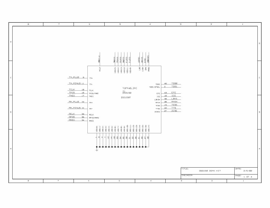
TCLK. On the right side of the board, jumper JP1 connects either the T3 oscillator output or the E3oscillator output to the intermediate node OSC. Install JP1 between top and middle posts for an E3 clockor between the middle and bottom posts for a T3 clock. Install jumper JP2 to connect the DS3150 TCLKpin to the OSC node. Leave JP2 uninstalled to source TCLK from the System Connector.
MCLK. Jumpers JP4 and JP6 control the DS3150 MCLK pin. Install jumper JP4 (and not JP6) toconnect the DS3150 MCLK pin to the OSC node. Install jumper JP6 (and not JP4) to connect the MCLKpin to VCC or GND. Leave both JP4 and JP6 uninstalled to source MCLK from the System Connector.
Figure 2. DS3150DK JUMPERS
EFE, ICE,LBKS*, LBO,RMON, TDS0,TDS1/OFSEL,TESS, TTS*and ZCSE*
VDD
GND
OSCE3
T3
MCLKVDD
GNDOSC SYSTEM CONNECTOR
TCLKOSC SYSTEM CONNECTOR
JP4JP6
JP2
JP1

DS3150DK
4 of 12
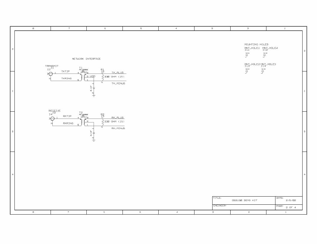
LINE-SIDE CONNECTIONSThe DS3150DK implements the Tx and Rx line-interface networks recommended in the DS3150 datasheet and shown in Figure 3. To connect the DS3150 to DS3, E3, or STS-1 test equipment, connect theequipment to BNC connectors J1 and J2 using coaxial cables. To externally loopback the DS3150 fromtransmitter to receiver, connect J1 and J2 together through a length of cable or a cable simulator.
Figure 3. DS3150DK LINE SIDE CIRCUITRY
SYSTEM CONNECTORThe 16-pin System Connector at the top of the board gives access to the following DS3150 signals:RPOS, TPOS, RNEG, TNEG, RCLK, TCLK, MCLK, and PRBS. Use the System Connector to connectthe DS3150 to an external framer or other data source/sink. To configure the DS3150DK board for anexternal remote loopback, place TCLK-RCLK, TPOS-RPOS, and TNEG-RNEG jumpers (Figure 4).
Figure 4. SYSTEM CONNECTOR
POWER SUPPLY CONNECTORSConnect a 3.3V power supply across the red (VCC) and black (GND) banana jacks. When a power supplyis present, the green PWR LED is lit.
GNDRPOSGNDTPOS
GND RNEG
GNDTNEG
GNDRCLK
GNDTCLK
GND MCLK
GND PRBS
DS3150
Tx+
Tx-
Rx+
Rx-
RECEIVE
1:2ct
1:2ct
R1330Ω(1%)
R2330Ω(1%)
TRANSMIT
J1
J2
T1
T2
VDD
0.1µF
0.1µF

DS3150DK
5 of 12
BASIC DS3150DK CONFIGURATIONTable 1, Table 2, and Table 3 list jumper settings for basic DS3150 configurations for T3, E3, and STS-1modes, respectively. These example configurations provide a quick start to using the DS3150DK andmay not be the proper configuration for your specific application. To set up other DS3150 configurationswith the DS3150DK, refer to the DS3150 data sheet for more details about configuration pins andoptions.
Table 1. BASIC T3 CONFIGURATION
SIGNALNAME
JUMPERPOSITION
GND VCC
JUMPER ACTION
ZCSE* JP13 B3ZS encoder/decoder enabledEFE JP8 Enhanced features enabledICE JP10 Normal RCLK, normal TCLKLBO JP12 Cable > 225ft
LBKS* JP14 No loopback enabledMCLK JP6 Don’t wire MCLK high or lowTTS* JP11 Enable transmit driver
RMON JP3 Disable 20dB preampTDS0 JP5TDS1 JP7 Transmit T3 AIS pattern
TESS JP9 T3 mode
SIGNALNAME
JUMPERPOSITION JUMPER ACTION
TCLK JP2 Source TCLK from OSC nodeMCLK JP4 Source MCLK from OSC node
SIGNALNAME
JUMPERPOSITION
T3 E3JUMPER ACTION
OSC JP1 Source OSC from T3 oscillator

DS3150DK
6 of 12
Table 2. BASIC E3 CONFIGURATION
SIGNALNAME
JUMPERPOSITION
GND VCC
JUMPER ACTION
ZCSE* JP13 HDB3 encoder/decoder enabledEFE JP8 Enhanced features enabledICE JP10 Normal RCLK, normal TCLKLBO JP12 Cable > 225ft
LBKS* JP14 No loopback enabledMCLK JP6 Don’t wire MCLK high or lowTTS* JP11 Enable transmit driver
RMON JP3 Disable 20dB preampTDS0 JP5TDS1 JP7
Transmit unframed all 1’s(E3 AIS)
TESS JP9 E3 mode
SIGNALNAME
JUMPERPOSITION JUMPER ACTION
TCLK JP2 Source TCLK from OSC nodeMCLK JP4 Source MCLK from OSC node
SIGNALNAME
JUMPERPOSITION
T3 E3JUMPER ACTION
OSC JP1 Source OSC from E3 oscillator
DS3150DK
7 of 12
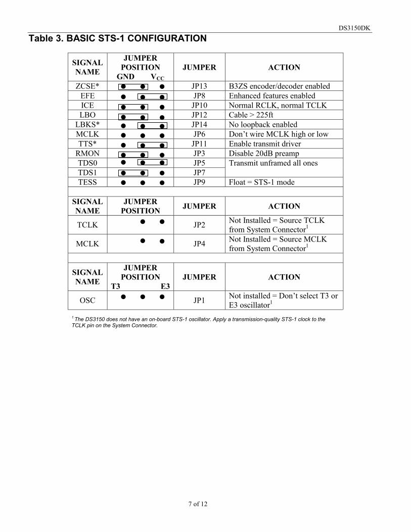
Table 3. BASIC STS-1 CONFIGURATION
SIGNALNAME
JUMPERPOSITION
GND VCC
JUMPER ACTION
ZCSE* JP13 B3ZS encoder/decoder enabledEFE JP8 Enhanced features enabledICE JP10 Normal RCLK, normal TCLKLBO JP12 Cable > 225ft
LBKS* JP14 No loopback enabledMCLK JP6 Don’t wire MCLK high or lowTTS* JP11 Enable transmit driver
RMON JP3 Disable 20dB preampTDS0 JP5TDS1 JP7
Transmit unframed all ones
TESS JP9 Float = STS-1 mode
SIGNALNAME
JUMPERPOSITION JUMPER ACTION
TCLK JP2 Not Installed = Source TCLKfrom System Connector1
MCLK JP4 Not Installed = Source MCLKfrom System Connector1
SIGNALNAME
JUMPERPOSITION
T3 E3JUMPER ACTION
OSC JP1 Not installed = Don’t select T3 orE3 oscillator1
1.The DS3150 does not have an on-board STS-1 oscillator. Apply a transmission-quality STS-1 clock to theTCLK pin on the System Connector.

DS3150DK
8 of 12
BILL OF MATERIALS
Table 4. BILL OF MATERIALS
ITEM DESCRIPTION MANUFACTURERPART NUMBER MANUFACTURER QTY ADDITIONAL
INFORMATIONREF
DESIGNATOR
1 3.3V Oscillator CPPX7-A5BC Cardinal Components 1 44.736MHzFrequency Y2
2 3.3V Oscillator CPPX7-A5BC Cardinal Components 1 34.368MHzFrequency Y1
3 T3/E3 SMDTransformer PE-65968 Pulse 2 T1, T2
4 Green SMD LED LN1351C-(TR) Panasonic 2 DS1, DS4
5 Red SMD LED LN1251C-(TR) Panasonic 2 DS2, DS3
6 DS3150 TQFP48 DS3150T Dallas Semiconductor 1 DS3150
7 MAX6316L MAX6316LUK26CY-T Maxim IntegratedProducts 1 U1
8 BNC CONN 2 J1, J2
9 Red Banana Jack 1646219 Mouser 1 VCC
10 Black Banana Jack 1646218 Mouser 1 GND
11 SMD 330Ω 3 Precision (1%) R1, R2, R5
12 SMD 68µF Cap 1 C14
13 SMD 350Ω 2 R11, R1314 SMD 100Ω 2 R7, R9
15 SMD 35Ω 5 R10, R14, R17,R18, R19
16 SMD 300Ω 1 R12
17 SMD 10kΩ 4 R3, R4, R15, R16
18 Protection Diode IN4001 1 D1
19 Jumper 3-Pin 12
JP1, JP3, JP5, JP6,JP7, JP8, JP9,JP10, JP11, JP12,JP13, JP14
20 Jumper 2-Pin 2 JP2, JP421 SMD 1µF CAP 3 C9, C10, C11
22 SMD 0.1µF CAP 7 C1, C2, C6, C7,C8, C12, C13
23 SMD 0.01µFCAP 3 C3, C4, C5
24 SMD 0.001µFCAP 2 C15, C16
25 MountingConnectors 4 I11, I12, I13, I14
26 16-Pin Header 1 J3