e1.1 circuit analysis problem sheet 1
TRANSCRIPT
Ver 3537 E1.1 Analysis of Circuits (2014)
E1.1 Circuit Analysis
Problem Sheet 1 (Lectures 1 & 2)
Key: [A]= easy ... [E]=hard
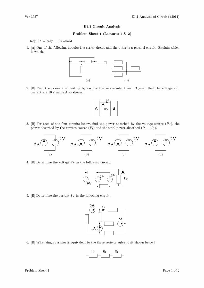
1. [A] One of the following circuits is a series circuit and the other is a parallel circuit. Explain whichis which.
(a) (b)
2. [B] Find the power absorbed by by each of the subcircuits A and B given that the voltage andcurrent are 10 V and 2 A as shown.
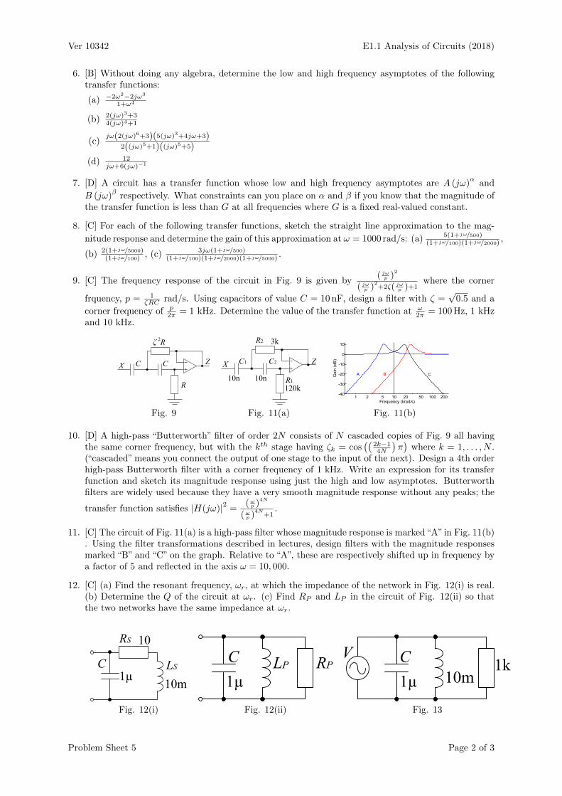
3. [B] For each of the four circuits below, find the power absorbed by the voltage source (PV ), thepower absorbed by the current source (PI) and the total power absorbed (PV + PI).
(a) (b) (c) (d)
4. [B] Determine the voltage VX in the following circuit.
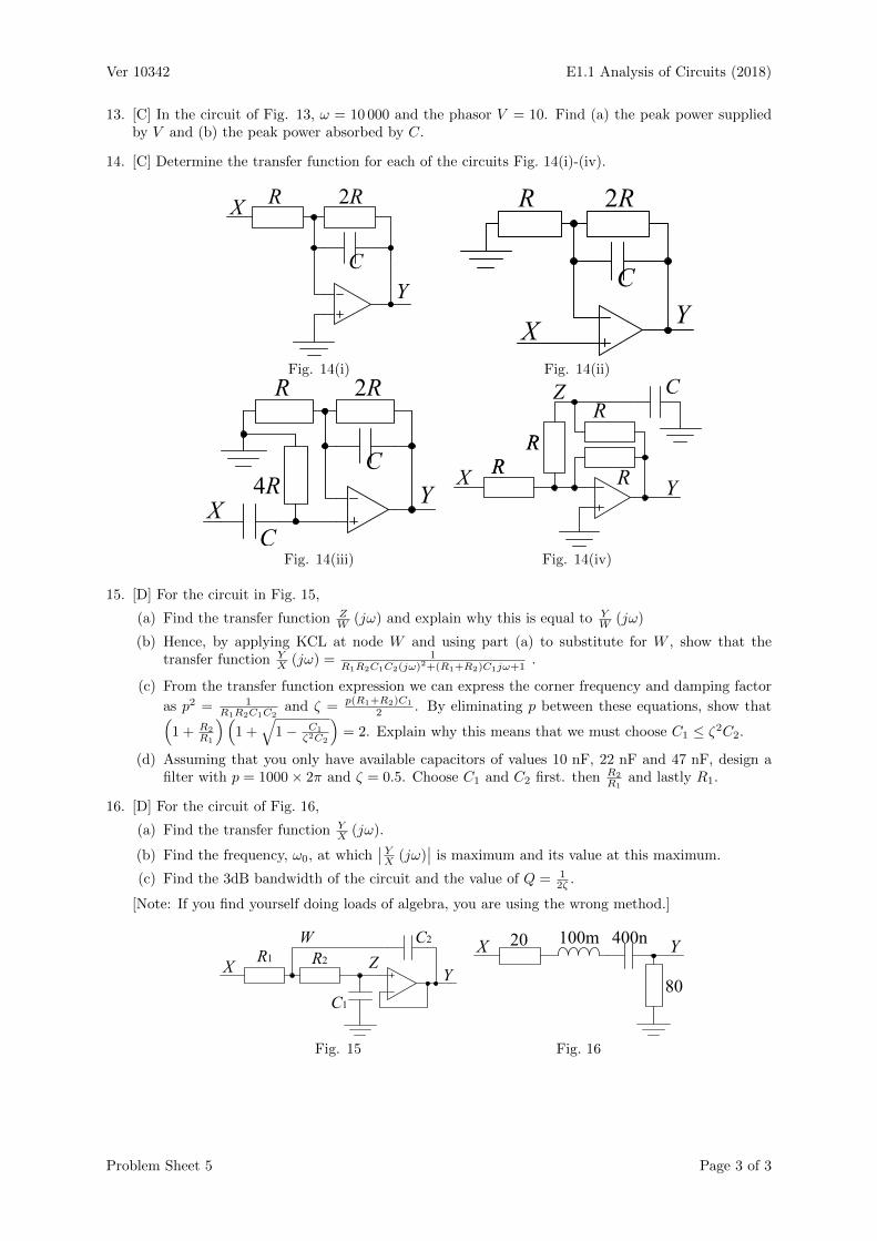
5. [B] Determine the current IX in the following circuit.
6. [B] What single resistor is equivalent to the three resistor sub-circuit shown below?
Problem Sheet 1 Page 1 of 2

Ver 3537 E1.1 Analysis of Circuits (2014)
7. [B] What single resistor is equivalent to the three resistor sub-circuit shown below?
8. [C] What single resistor is equivalent to the five resistor sub-circuit shown below?
9. [A] If a resistor has a conductance of 8µS, what is its resistance?
10. [B] Determine the voltage across each of the resistors in the following circuit and the power dissipatedin each of them. Calculate the power supplied by the voltage source.
11. [B] Determine the current through each of the resistors in the following circuit and the power dissip-ated in each of them. Calculate the power supplied by the current source.
12. [B] Determine R1 so that Y = 14X.
13. [B] Choose R1 and R2 so that Y = 0.1X and R1 +R2 = 10 MΩ.
14. [D] You have a supply of resistors that have the values 10, 12, 15, 18, 22, 27, 33, 39, 47, 56, 68, 82 ×10n Ω for all integer values of n. Thus, for example, a resistor of 390 Ω is available and the next highervalue is 470 Ω. Show how, by combining two resistors in each case, it is possible to make networkswhose equivalent resistance is (a) 3 kΩ, (b) 4 kΩ and (c) as close as possible to 3.5 kΩ. Determine isthe worst case percentage error that might arise if, instead of combining resistors, you just pick theclosest one available.
Problem Sheet 1 Page 2 of 2
Ver 2427 E1.1 Analysis of Circuits (2014)
E1.1 Circuit Analysis
Problem Sheet 1 - Solutions
1. Circuit (a) is a parallel circuit: there are only two nodes and all four components are connectedbetween them.
Circuit (b) is a series circuit: each node is connected to exactly two components and the same currentmust flow through each.
2. For subcircuit B the voltage and current correspond to the passive sign convention (i.e. the currentarrow in the opposite direction to the voltage arrow) and so the power absorbed by B is given byV × I = 20 W.
For device A we need to reverse the direction of the current to conform to the passive sign convention.Therefore the power absorbed by A is V ×−I = −20 W.
As must always be true, the total power absorbed by all components is zero.
3. The power absorbed is positive if the voltage and current arrows go in opposite directions and negativeif they go in the same direction. So we get: (a) PV = +4, PI = −4, (b) PV = +4, PI = −4, (c)PV = −4, PI = +4, (a) PV = −4, PI = +4. In all cases, the total power absorbed is PV + PI = 0.
4. We can find a path (shown highlighted below) from the bottom to the top of the VX arrow thatpasses only through voltage sources and so we just add these up to get the total potential difference:VX = (−3) + (+2) + (+9) = +8 V.
5. If we add up the currents flowing out of the region shown highlighted below, we obtain IX−5−1+2 =0. Hence IX = 4 A.
6. The three series resistors are equivalent to a single resistor with a value of 1 + 5 + 2 = 8 kΩ.
7. The three series resistors are equivalent to a single resistor with a value of 11/1+1/5+1/2 = 1
1.7 =
0.588 kΩ.
8. We can first combine the parallel 2 k and 3 k resistors to give 2×32+3 = 1.2 k. This is then in series with
the 4 k resistor which makes 5.2 k in all. Now we just have three resistors in parallel to give a totalof 1
1/1+1/5+1/5.2 = 11.39 = 0.718kΩ.
9. The resistance is 18×10−6 = 125 kΩ
Solution Sheet 1 Page 1 of 2
Ver 2427 E1.1 Analysis of Circuits (2014)
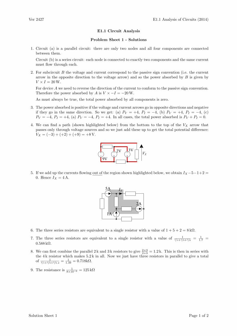
10. [Method 1]: The resistors are in series and so form a potential divider. The total series resistance is7 k, so the voltages across the three resistors are 14× 1
7 = 2 V, 14× 27 = 4 V and 14× 4
7 = 8 V. The
power dissipated in a resistor is V 2
R , so for the three resistors, this gives 22
1 = 4 mW, 42
2 = 8 mW and82
4 = 16 mW.
[Method 2]: The total resistance is is 7 k so the current flowing in the circuit is 147 = 2 mA. The voltage
across a resistor is IR which, in for these resistors, gives 2× 1 = 2 V, 2× 2 = 4 V and 2× 4 = 8 V.The power dissipated is V I which gives 2 × 2 = 4 mW, 4 × 2 = 8 mW and 8 × 2 = 16 mW. Thecurrent through the voltage source is 2 mA, so the power it is supplying is V I = 14 × 2 = 28 mW.This is, inevitably, equal to the sum of the power disspipated by the three resistors: 4+8+16 = 28.
11. [Method 1]: The resistors are in parallel and so form a current divider: the 21 mA will divide inproportion to the conductances: 1 mS, 0.5 mS and 0.25 mS. The total conductance is 1.75 mS, so thethree resistor currents are 21 × 1
1.75 = 12 mA, 21 × 0.51.75 = 6 mA and 21 × 0.25
1.75 = 3 mA. The powerdissipated in a resistor is I2R which gives 122 × 1 = 144 mW, 62 × 2 = 72 mW and 32 × 4 = 36 mW.
[Method 2]: The equivalent resistance of the three resistors is 11/1+1/2+1/4 = 4
7 kΩ. Therefore the
voltage across all components in the parallel circuit is 21× 47 = 12 V. The current through a resistor
is VR which gives 12
1 = 12 mA,122 = 6 mA and124 = 3 mA. The power dissipated in a resistor is V I
which gives 12 × 12 = 144 mW, 12 × 6 = 72 mW and 12 × 3 = 36 mW. The power supplied by thecurrent source is 12× 21 = 252 mW which as expected equals 144 + 72 + 36.
12. The resistors form a potential divider, so YX = 4
R1+4 . So we want 4R1+4 = 1
4 ⇒ R1 + 4 = 16 ⇒R1 = 12 k.
13. The resistors form a potential divider, so YX = R2
R1+R2. So we want R2
R1+R2= 1
10 and R1 + R2 =10 MΩ. Substituting one into the other and cross-multiplying gives 10R2 = 10 MΩ ⇒ R2 = 1 MΩ.Substituting this into the simpler of the two initial equations gives R1 = 10− 1 = 9 MΩ.
14. (a) 3 k = 1.5 k + 1.5 k = 3.3 k||33 k, (b) 4 k = 3.9 k + 100, (c) 3.488 k = 3.9 k||33 k.
To make an exhaustive search for creating a resistance of R, you need to consider two possibilities:(i) for two resistors in series, the largest of the two resistors must be in the range [ 12R,R] or (ii) fortwo resistors in parallel, the smallest resistor must be in the range [R, 2R]. In both cases there areat most four possibilities, so you need to consider up to eight possibilities in all. So, for example, forR = 3.5 k, we would consider the following possibilities: (i) 1.5 k + 1.8 k = 3.3 k, 1.8 k + 1.8 k = 3.6 k,2.2 k + 1.2 k = 3.4 k, 2.7 k + 0.82 k = 3.52 k and (ii) 3.9 k||33 k = 3.488 k, 4.7 k||15 k = 3.579 k,5.6 k||10 k = 3.59 k, 6.8 k||6.8 k = 3.4 k. The choice with least error is the one given above.
Since we are interested in % errors, we need to consider the ratio between resistor values. The largestratio between successive resistors is the series is 15
12 = 1.25 (this includes the wraparound ratio of10082 = 1.22). The worst-case percentage error will arise if our target resistance is the mean of these
two values, 13.5. The percentage error in choosing either one is then 1.513.5 = 11.1%.
Solution Sheet 1 Page 2 of 2
Ver 2427 E1.1 Analysis of Circuits (2015)
E1.1 Circuit Analysis
Problem Sheet 2 (Lectures 3 & 4)
Key: [A]= easy ... [E]=hard
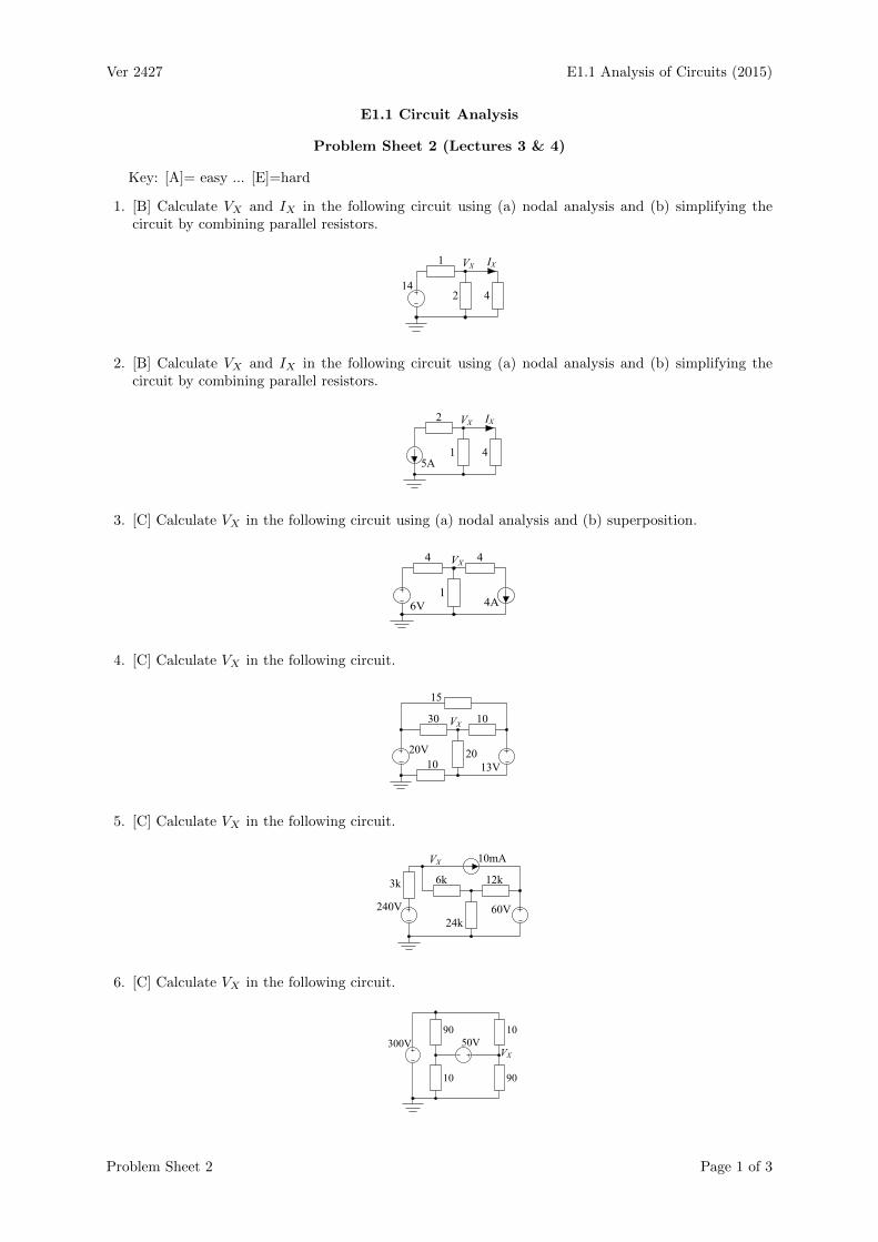
1. [B] Calculate VX and IX in the following circuit using (a) nodal analysis and (b) simplifying thecircuit by combining parallel resistors.
2. [B] Calculate VX and IX in the following circuit using (a) nodal analysis and (b) simplifying thecircuit by combining parallel resistors.
3. [C] Calculate VX in the following circuit using (a) nodal analysis and (b) superposition.
4. [C] Calculate VX in the following circuit.
5. [C] Calculate VX in the following circuit.
6. [C] Calculate VX in the following circuit.
Problem Sheet 2 Page 1 of 3

Ver 2427 E1.1 Analysis of Circuits (2015)
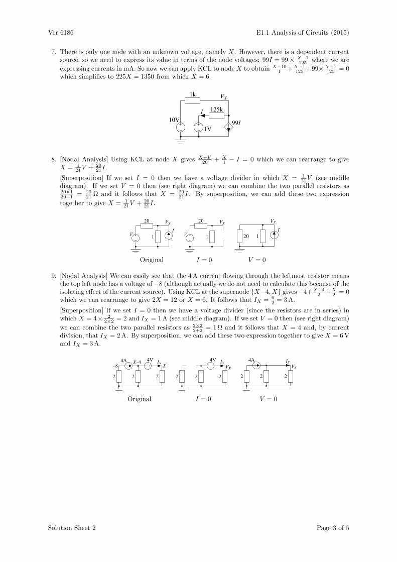
7. [C] Calculate VX in the following circuit. The value of the dependent current source is 99 time thecurrent flowing through the 1 V voltage source.
8. [C] In the following circuit calculate VX in terms of V and I using (a) nodal analysis and (b)superposition.
9. [C] Calculate VX and IX in the following circuit using (a) nodal analysis and (b) superposition.
10. [C] Determine an expression for IX in terms of V in the following circuit. Determine the value of Vthat will make IX = 0.
11. [C] Calculate VX in the following circuit using (a) nodal analysis and (b) superposition.
12. [C] Calculate VX in the following circuit which includes a dependent voltage source.
Problem Sheet 2 Page 2 of 3
Ver 2427 E1.1 Analysis of Circuits (2015)
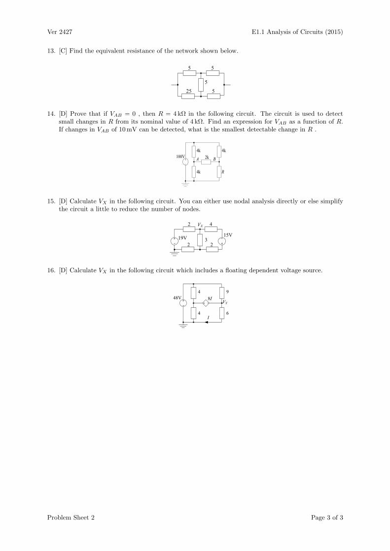
13. [C] Find the equivalent resistance of the network shown below.
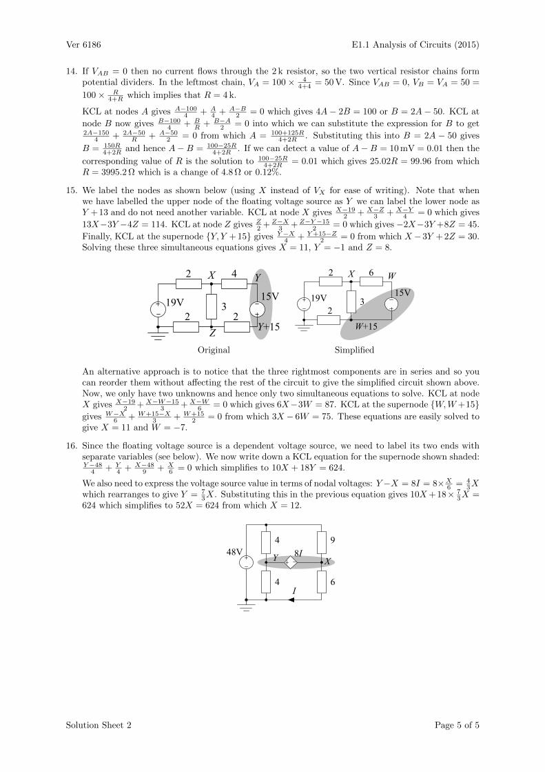
14. [D] Prove that if VAB = 0 , then R = 4 kΩ in the following circuit. The circuit is used to detectsmall changes in R from its nominal value of 4 kΩ. Find an expression for VAB as a function of R.If changes in VAB of 10 mV can be detected, what is the smallest detectable change in R .
15. [D] Calculate VX in the following circuit. You can either use nodal analysis directly or else simplifythe circuit a little to reduce the number of nodes.
16. [D] Calculate VX in the following circuit which includes a floating dependent voltage source.
Problem Sheet 2 Page 3 of 3

Ver 6186 E1.1 Analysis of Circuits (2015)
E1.1 Circuit Analysis
Problem Sheet 2 - Solutions
Note: In many of the solutions below I have written the voltage at node X as the variable X instead ofVX in order to save writing so many subscripts.
1. [Nodal analysis] KCL at node VX gives VX−141 + VX
2 + VX
4 = 0 which simplifies to 7VX − 56 = 0 fromwhich VX = 8.
[Parallel resistors] We can merge the 2 Ω and 4 Ω resistors to make one of 2×42+4 = 4
3 Ω as shown below.
Now we have a potential divider, so VX = 14× 1.332.33 = 8 V.
In both cases, we can now calculate IX = VX
4 = 2 A. Note that when we merge the two resistors, IXis no longer a distinct current on the diagram.
Original Simplified
2. [Nodal Analysis] KCL at node Vx gives 5 + VX
1 + VX
4 = 0 which simplifies to 20 + 5VX = 0 fromwhich VX = −4.
[Parallel Resistors] We can combine the 1 Ω and 4 Ω resistors to make one of 1×41+4 = 4
5 Ω as shownbelow. Now we have VX = −5× 0.8 = −4 V.
Original Simplified
In both cases, we can now calculate IX = VX
4 = −1 A.
In this question, you have to be a bit careful about the sign used to represent currents. Whenever youuse Ohm’s law, you must be sure that you use the passive sign convention (with the current arrowin the opposite direction to the voltage arrow); this is why the current through the 0.8 Ω resistor is−5 A rather than +5 A.
Solution Sheet 2 Page 1 of 5

Ver 6186 E1.1 Analysis of Circuits (2015)
3. [Nodal Analysis] KCL at node Vx gives VX−64 + VX
1 + 4 = 0 which simplifies to 5VX + 10 = 0 fromwhich VX = −2.
[Superposition] (i) If we set the current source to zero, then the 4 Ω resistor connected to it playsno part in the circuit and we have a potential divider giving VX = 6× 1
5 = 1.2. (ii) We now set thevoltage source to zero and then simplify the resultant circuit as shown below. Being careful withsigns, we now get VX = −4 × 0.8 = −3.2. Adding these two values together gives a final answer ofVX = −2.
Original I = 0 V = 0 V = 0 simplified
4. We first label the nodes; we only need two variables because of the floating voltage source. KCL
at X gives X−2030 + X−(Y−13)
20 + X−Y10 = 0 which gives 11X − 9Y = 1. KCL at the supernode
Y, Y − 13gives Y−2015 + Y−X
10 + (Y−13)−X20 + (Y−13)
10 = 0 which gives −9X + 19Y = 197. Solvingthese two simultaneous equations gives X = 14 and Y = 17.
5. We first label the nodes; there are only two whose voltage is unknown. Working in mA and kΩ, KCLat X gives X−240
3 + X−Y6 +10 = 0 which gives 3X−Y = 420. KCL at Y gives Y−X
6 + Y24 + Y−60
12 = 0which gives −4X + 7Y = 120. Solving these simultaneous equations gives X = 180 and Y = 120.
6. We first label the nodes; since the two nodes having unknown voltages are joined by a fixed voltagesource, we only need one variable. We write down KCL for the supernode X,X − 50 (shaded in
the diagram) which gives (X−50)−30090 + (X−50)
10 + X−30010 + X
90 = 0 which simplifies to 20X = 3500 orX = 175 V.
Solution Sheet 2 Page 2 of 5
Ver 6186 E1.1 Analysis of Circuits (2015)
7. There is only one node with an unknown voltage, namely X. However, there is a dependent currentsource, so we need to express its value in terms of the node voltages: 99I = 99× X−1
125 where we are
expressing currents in mA. So now we can apply KCL to node X to obtain X−101 + X−1
125 +99×X−1125 = 0
which simplifies to 225X = 1350 from which X = 6.
8. [Nodal Analysis] Using KCL at node X gives X−V20 + X
1 − I = 0 which we can rearrange to giveX = 1
21V + 2021I.
[Superposition] If we set I = 0 then we have a voltage divider in which X = 121V (see middle
diagram). If we set V = 0 then (see right diagram) we can combine the two parallel resistors as20×120+1 = 20
21 Ω and it follows that X = 2021I. By superposition, we can add these two expression
together to give X = 121V + 20
21I.
Original I = 0 V = 0
9. [Nodal Analysis] We can easily see that the 4 A current flowing through the leftmost resistor meansthe top left node has a voltage of −8 (although actually we do not need to calculate this because of theisolating effect of the current source). Using KCL at the supernode X−4, X gives−4+X−4
2 +X2 = 0
which we can rearrange to give 2X = 12 or X = 6. It follows that IX = 62 = 3 A.
[Superposition] If we set I = 0 then we have a voltage divider (since the resistors are in series) inwhich X = 4× 2
2×2 = 2 and IX = 1 A (see middle diagram). If we set V = 0 then (see right diagram)
we can combine the two parallel resistors as 2×22+2 = 1 Ω and it follows that X = 4 and, by current
division, that IX = 2 A. By superposition, we can add these two expression together to give X = 6 Vand IX = 3 A.
Original I = 0 V = 0
Solution Sheet 2 Page 3 of 5

Ver 6186 E1.1 Analysis of Circuits (2015)
10. [Nodal Analysis] We first label the unknown node as X. Now, KCL at this node gives−6+X3 +X−V
6 =
0 which rearranges to give 3X = V + 36 from which X = 13V + 12. Now IX = X
3 so IX = 19V + 4.
[Superposition] If we set I = 0 (see middle diagram) then IX = V9 . If we set V = 0 then (see
right diagram) we have a current divider in which the 6 A current divides in proportion to the
conductances. So IX = 6× 1/31/3+1/6 = 6× 2
3 = 4. Adding these results together gives IX = 19V + 4.
If V = −36 then IX = 0.
Original I = 0 V = 0
11. [Nodal Analysis] KCL at node X gives X−102 + X
2 + X−(−3)3 = 0 which rearranges to give 8X = 24
from which X = 3.
[Superposition] If we set the left source to zero (see middle diagram) then, the two parallel 2 Ωresistors are equivalent to 1 Ω and so we have a potential divider and X = −3 × 1
4 = −0.75. If weset the other source to zero (see right diagram) we can combine the 2 Ω and 3 Ω parallel resistors toobtain 2×3
2+3 = 1.2 Ω. We again have a potential divider giving X = 10× 1.22+1.2 = 3.75. Adding these
together gives X = −0.75 + 3.75 = 3 V.
Original U1 = 0 U2 = 0
12. KCL at node Y gives Y−41 + Y−X
5 = 0 which rearranges to −X+6Y = 20. We also have the equationof the dependent voltage source: X = −6Y . We can conveninetly eliminate 6Y between these twoto give −2X = 20 and so X = −10.
13. We first pick a ground reference at one end of the network and label all the other nodes. Theequivalent resistance is now V
I . We assume that we know V and then calculate I. KCL at node
A gives A−V5 + A−B
5 + A5 = 0 from which 3A − B = V or B = 3A − V . KCL at node B gives
B−V25 + B−A
5 + B5 = 0 from which 11B − 5A = V . Substituting B = 3A− V into this equation gives
33A− 5A = 12V or A = 1228V which in turn gives B = 3A− V = 8
28V . The current I is the sum of
the currents throught the rightmost two 5 Ωresistors: I = A5 + B
5 = 17V . So the equivalent resistance
is VI = 7 Ω.
Solution Sheet 2 Page 4 of 5
Ver 6186 E1.1 Analysis of Circuits (2015)
14. If VAB = 0 then no current flows through the 2 k resistor, so the two vertical resistor chains formpotential dividers. In the leftmost chain, VA = 100× 4
4+4 = 50 V. Since VAB = 0, VB = VA = 50 =
100× R4+R which implies that R = 4 k.
KCL at nodes A gives A−1004 + A
4 + A−B2 = 0 which gives 4A− 2B = 100 or B = 2A− 50. KCL at
node B now gives B−1004 + B
R + B−A2 = 0 into which we can substitute the expression for B to get
2A−1504 + 2A−50
R + A−502 = 0 from which A = 100+125R
4+2R . Substituting this into B = 2A − 50 gives
B = 150R4+2R and hence A−B = 100−25R
4+2R . If we can detect a value of A−B = 10 mV = 0.01 then the
corresponding value of R is the solution to 100−25R4+2R = 0.01 which gives 25.02R = 99.96 from which
R = 3995.2 Ω which is a change of 4.8 Ω or 0.12%.
15. We label the nodes as shown below (using X instead of VX for ease of writing). Note that whenwe have labelled the upper node of the floating voltage source as Y we can label the lower node asY +13 and do not need another variable. KCL at node X gives X−19
2 + X−Z3 + X−Y
4 = 0 which gives
13X−3Y −4Z = 114. KCL at node Z gives Z2 + Z−X
3 + Z−Y−152 = 0 which gives −2X−3Y +8Z = 45.
Finally, KCL at the supernode Y, Y + 15 gives Y−X4 + Y+15−Z
2 = 0 from which X−3Y + 2Z = 30.Solving these three simultaneous equations gives X = 11, Y = −1 and Z = 8.
Original Simplified
An alternative approach is to notice that the three rightmost components are in series and so youcan reorder them without affecting the rest of the circuit to give the simplified circuit shown above.Now, we only have two unknowns and hence only two simultaneous equations to solve. KCL at nodeX gives X−19
2 + X−W−153 + X−W
6 = 0 which gives 6X−3W = 87. KCL at the supernode W,W +15gives W−X
6 + W+15−X3 + W+15
2 = 0 from which 3X − 6W = 75. These equations are easily solved togive X = 11 and W = −7.
16. Since the floating voltage source is a dependent voltage source, we need to label its two ends withseparate variables (see below). We now write down a KCL equation for the supernode shown shaded:Y−48
4 + Y4 + X−48
9 + X6 = 0 which simplifies to 10X + 18Y = 624.
We also need to express the voltage source value in terms of nodal voltages: Y −X = 8I = 8×X6 = 4
3Xwhich rearranges to give Y = 7
3X. Substituting this in the previous equation gives 10X +18× 73X =
624 which simplifies to 52X = 624 from which X = 12.
Solution Sheet 2 Page 5 of 5

Ver 2379 E1.1 Analysis of Circuits (2014)
E1.1 Circuit Analysis
Problem Sheet 3 (Lectures 5, 6, 7 & 8)
Key: [A]= easy ... [E]=hard
1. [B] Calculate the Thevenin and Norton equivalent networks at the terminals A and B for each ofthe following.
(a) (b)
2. [B] Use nodal analysis to calculate an expression for A in Fig. 2 in terms of I and then rearrangethis to give I in terms of A. Show how these expressions are related to the Thevenin and Nortonequivalent networks at the terminals A and B.
Fig. 2 Fig. 3 Fig. 4
3. [B] Determine X in Fig. 3 when (a) U = +5 V and (b) U = −5 V. Assume that the diode has aforward voltage drop of 0.7 V.
4. [B] In Fig. 4, calculate I and the power dissipation in the resistor and in the diode. Assume thatthe diode has a forward voltage drop of 0.7 V.
5. [B] Find the gains XU and Y
U in the following circuits:
(a) (b)
6. [C] Calculate the Thevenin and Norton equivalent networks at the terminals A and B in Fig. 6 intwo ways (a) by combining resistors to simplify the circuit and (b) by using nodal analysis to expressA in terms of I.
Fig. 6
Problem Sheet 3 Page 1 of 5
Ver 2379 E1.1 Analysis of Circuits (2014)
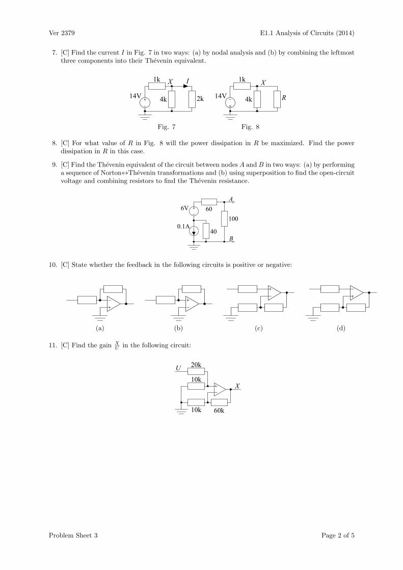
7. [C] Find the current I in Fig. 7 in two ways: (a) by nodal analysis and (b) by combining the leftmostthree components into their Thevenin equivalent.
Fig. 7 Fig. 8
8. [C] For what value of R in Fig. 8 will the power dissipation in R be maximized. Find the powerdissipation in R in this case.
9. [C] Find the Thevenin equivalent of the circuit between nodes A and B in two ways: (a) by performinga sequence of Norton↔Thevenin transformations and (b) using superposition to find the open-circuitvoltage and combining resistors to find the Thevenin resistance.
10. [C] State whether the feedback in the following circuits is positive or negative:
(a) (b) (c) (d)
11. [C] Find the gain XU in the following circuit:
Problem Sheet 3 Page 2 of 5
Ver 2379 E1.1 Analysis of Circuits (2014)
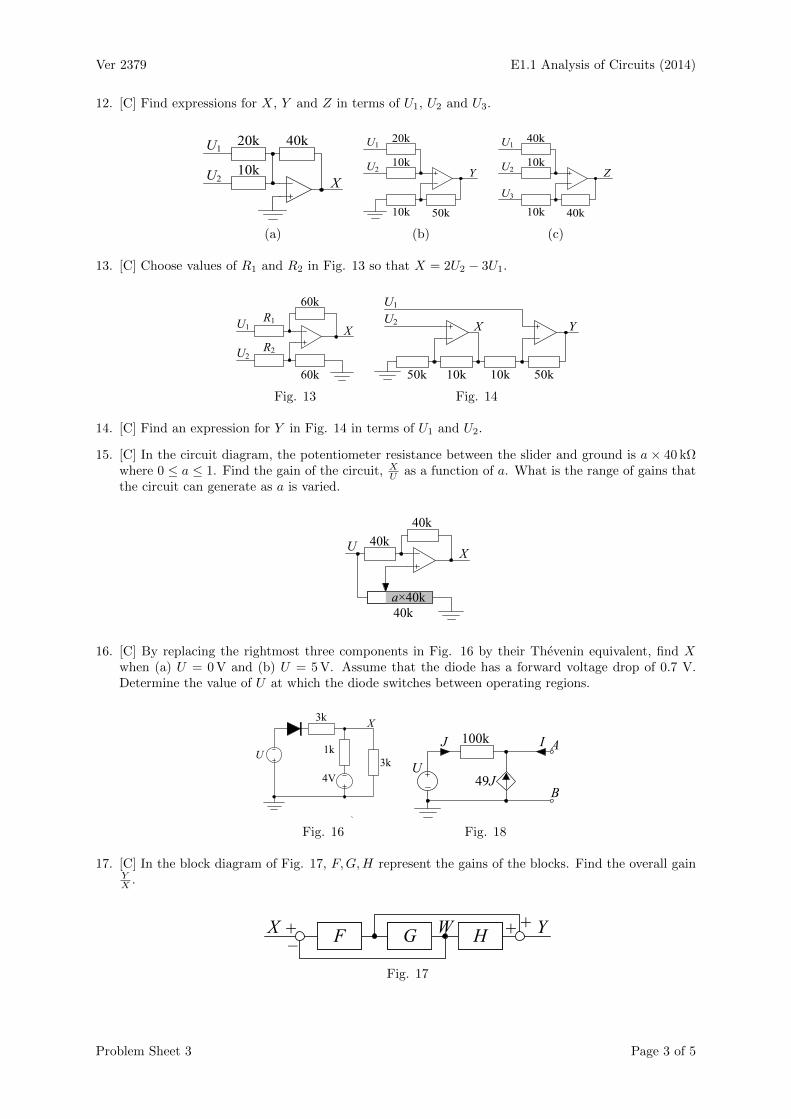
12. [C] Find expressions for X, Y and Z in terms of U1, U2 and U3.
(a) (b) (c)
13. [C] Choose values of R1 and R2 in Fig. 13 so that X = 2U2 − 3U1.
Fig. 13 Fig. 14
14. [C] Find an expression for Y in Fig. 14 in terms of U1 and U2.
15. [C] In the circuit diagram, the potentiometer resistance between the slider and ground is a× 40 kΩwhere 0 ≤ a ≤ 1. Find the gain of the circuit, X
U as a function of a. What is the range of gains thatthe circuit can generate as a is varied.
16. [C] By replacing the rightmost three components in Fig. 16 by their Thevenin equivalent, find Xwhen (a) U = 0 V and (b) U = 5 V. Assume that the diode has a forward voltage drop of 0.7 V.Determine the value of U at which the diode switches between operating regions.
Fig. 16 Fig. 18
17. [C] In the block diagram of Fig. 17, F,G,H represent the gains of the blocks. Find the overall gainYX .
Fig. 17
Problem Sheet 3 Page 3 of 5
Ver 2379 E1.1 Analysis of Circuits (2014)
18. [D] The circuit of Fig. 18 includes a dependent current source whose value is proportional to thecurrent J . Find the Thevenin equivalent of the circuit by two methods: (a) use nodal analysisincluding the current I and express the voltage VAB as a function of I and (b) assume I = 0 andfind (i) the open circuit voltage, VAB as a function of U and (ii) the short-circuit current (with Ajoined to B) as a function of U . Hence find the Thevenin equivalent of the circuit.
19. [D] Choose resistor values in Fig. 19 so that (a) X = 12U3 + 1
3U2 + 16U1 and (b) the Thevenin
resistance between X and ground is 50 Ω. Why would the question be impossible if it had asked forX = 1
2U3 + 13U2 + 1
3U1?
Fig. 19 Fig. 20
20. [D] Choose resistor values in Fig. 20 so that (a) the Thevenin between X and ground is 50 Ω and(b) it is possible to set X to 1, 2, 3 or 4 V by setting the switches appropriately.
21. [D] State whether the feedback in the following circuits is positive or negative:
(a) (b)
Problem Sheet 3 Page 4 of 5
Ver 2379 E1.1 Analysis of Circuits (2014)
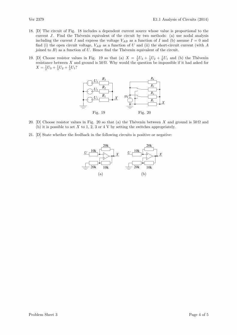
22. [D] Find an expression for Z in Fig. 22 in terms of U1 and U2.
Fig. 22 Fig. 23
23. [D] The circuit of Fig. 23 is called a Howland current source. Show that the circuit has negativefeedback. Use nodal analysis to determine the current I and show that it does not depend on R.
24. [D] A non-linear device has a characteristic Y =√X for inputs in the range 0 ≤ X ≤ 1. To improve
its linearity, the device is placed in a feedback loop using an op-amp with a gain of A as shown inFig. 24. Determine an expression for Y in terms of U and A. Simplify the expression by using the
Taylor series approximation:√v + w ≈
√v(
1 + w2v −
w2
8v2
)valid for v w. Estimate how large A
must be to ensure that Y |U=0.5 = 0.5× Y |U=1 to within 1% of Y |U=1.
Fig. 24
25. [D] The diodes in Fig. 25 have a characteristic I = k exp VVT
where VT = 25 mV.
(a) For the circuit of in Fig. 25(a), find an expression for U in terms of X assuming that X > 0.
(b) For the circuit of in Fig. 25(b), find and expression for Y in terms of X assuming that X > 0.
Fig. 25(a) Fig. 25(b)
26. [C] We normally assume that the current at the inputs to an opamp are negligible. However this is notalways true and this question investigates the effect of non-zero input bias currents. If IB = 100 nA,find expressions for X
U and YU in the circuits below. Explain the advantage of circuit (b) and derive
a general principal that should be followed when using opamps having non-negligible input biascurrents, IB .
(a) (b)
Problem Sheet 3 Page 5 of 5
Ver 9024 E1.1 Analysis of Circuits (2016)
E1.1 Circuit Analysis
Problem Sheet 3 - Solutions
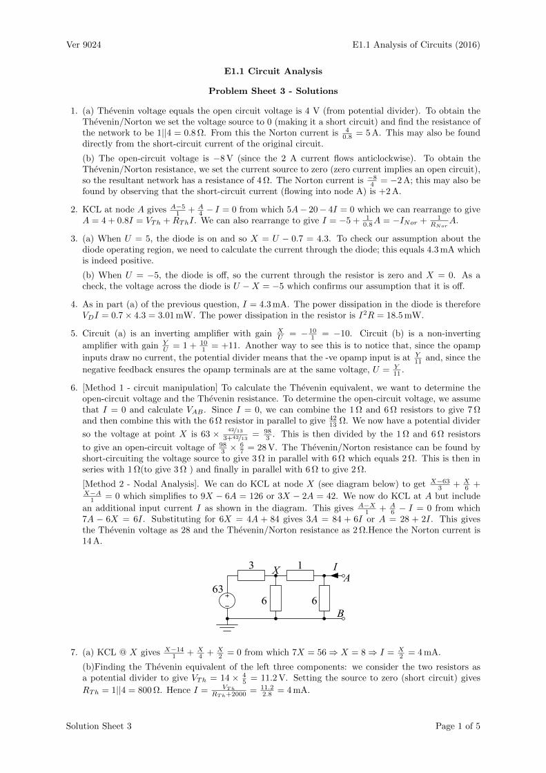
1. (a) Thevenin voltage equals the open circuit voltage is 4 V (from potential divider). To obtain theThevenin/Norton we set the voltage source to 0 (making it a short circuit) and find the resistance ofthe network to be 1||4 = 0.8 Ω. From this the Norton current is 4
0.8 = 5 A. This may also be founddirectly from the short-circuit current of the original circuit.
(b) The open-circuit voltage is −8 V (since the 2 A current flows anticlockwise). To obtain theThevenin/Norton resistance, we set the current source to zero (zero current implies an open circuit),so the resultant network has a resistance of 4 Ω. The Norton current is −84 = −2 A; this may also befound by observing that the short-circuit current (flowing into node A) is +2 A.
2. KCL at node A gives A−51 + A
4 − I = 0 from which 5A− 20− 4I = 0 which we can rearrange to giveA = 4 + 0.8I = VTh +RThI. We can also rearrange to give I = −5 + 1
0.8A = −INor + 1RNor
A.
3. (a) When U = 5, the diode is on and so X = U − 0.7 = 4.3. To check our assumption about thediode operating region, we need to calculate the current through the diode; this equals 4.3 mA whichis indeed positive.
(b) When U = −5, the diode is off, so the current through the resistor is zero and X = 0. As acheck, the voltage across the diode is U −X = −5 which confirms our assumption that it is off.
4. As in part (a) of the previous question, I = 4.3 mA. The power dissipation in the diode is thereforeVDI = 0.7× 4.3 = 3.01 mW. The power dissipation in the resistor is I2R = 18.5 mW.
5. Circuit (a) is an inverting amplifier with gain XU = − 10
1 = −10. Circuit (b) is a non-inverting
amplifier with gain YU = 1 + 10
1 = +11. Another way to see this is to notice that, since the opamp
inputs draw no current, the potential divider means that the -ve opamp input is at Y11 and, since the
negative feedback ensures the opamp terminals are at the same voltage, U = Y11 .
6. [Method 1 - circuit manipulation] To calculate the Thevenin equivalent, we want to determine theopen-circuit voltage and the Thevenin resistance. To determine the open-circuit voltage, we assumethat I = 0 and calculate VAB . Since I = 0, we can combine the 1 Ω and 6 Ω resistors to give 7 Ωand then combine this with the 6 Ω resistor in parallel to give 42
13 Ω. We now have a potential divider
so the voltage at point X is 63 × 42/133+42/13 = 98
3 . This is then divided by the 1 Ω and 6 Ω resistors
to give an open-circuit voltage of 983 ×
67 = 28 V. The Thevenin/Norton resistance can be found by
short-circuiting the voltage source to give 3 Ω in parallel with 6 Ω which equals 2 Ω. This is then inseries with 1 Ω(to give 3 Ω ) and finally in parallel with 6 Ω to give 2 Ω.
[Method 2 - Nodal Analysis]. We can do KCL at node X (see diagram below) to get X−633 + X
6 +X−A
1 = 0 which simplifies to 9X − 6A = 126 or 3X − 2A = 42. We now do KCL at A but include
an additional input current I as shown in the diagram. This gives A−X1 + A
6 − I = 0 from which7A − 6X = 6I. Substituting for 6X = 4A + 84 gives 3A = 84 + 6I or A = 28 + 2I. This givesthe Thevenin voltage as 28 and the Thevenin/Norton resistance as 2 Ω.Hence the Norton current is14 A.
7. (a) KCL @ X gives X−141 + X
4 + X2 = 0 from which 7X = 56⇒ X = 8⇒ I = X
2 = 4 mA.
(b)Finding the Thevenin equivalent of the left three components: we consider the two resistors asa potential divider to give VTh = 14 × 4
5 = 11.2 V. Setting the source to zero (short circuit) gives
RTh = 1||4 = 800 Ω. Hence I = VTh
RTh+2000 = 11.22.8 = 4 mA.
Solution Sheet 3 Page 1 of 5

Ver 9024 E1.1 Analysis of Circuits (2016)
8. From question 7, the left three components have a Thevenin equivalent: VTh = 11.2 V and RTh =800 Ω. It follows that the maximum power will be dissipated in R when R = RTh = 800 Ω (see notespage 5-8). Since the voltage across R will then be 1
2VTh the power dissipation will be 14RTh
V 2Th =
39.2 mW.
9. (a) As shown in the sequence below, we first combine the current source with the 40 Ωresistor, thencombine the four series components into a single Thevenin equivalent and finally find the Theveninequivalent of the simple network (using parallel resistors for RTh and a potential divider for VTh).
(b) Setting the voltage source to zero gives us the first diagram. Combining 40||(60 + 100) = 32 soX = −0.1× 32 = −3.2 V. it follows (potential divider) that A = −3.2× 100
160 = −2 V.
Now setting the current source to zero gives the second diagram and we have a potential dividergiving VAB = 6× 100
100+60+40 = 3 V.
Superposition now gives us VAB = VTh = −2 + 3 = 1 V.
To find RTh we set both sources to zero and find the resultant resistance of 100||(60+40) = 100||100 =50 Ω.
10. (a) Negative, (b) Positive, (c) Negative, (d) Positive. In simple circuits like these, you can just seewhich terminal the output feeds back to.
11. The best way to think of this circuit is as a potential divider with gain YU = 1
3 followed by a
non-inverting opamp circuit with gain XY = 1 + 60
10 = 7. The combined gain is then XU =1
3 × 7 = 73 .
Solution Sheet 3 Page 2 of 5
Ver 9024 E1.1 Analysis of Circuits (2016)
12. (a) You can either recognise this a a standard inverting summing amplifier with gainX = −
(4020U1 + 40
10U2
)= −2U1−4U2 or else apply KCL at the +ve input terminal with the assump-
tion that negative feedback will ensure that this terminal is at the same voltage as the –ve terminali.e. 0 V. This gives: 0−U1
20 + 0−U2
10 + 0−X40 = 0 from which X = −2U1 − 4U2.
(b) The network connected to the +ve terminal is a weighted averaging circuit (page 3-7 of the notes)so V+ = 1
3U1 + 23U2. The opamp circuit itself is a non-inverting amplifier with a gain of 1 + 50
10 = 6.So, Y = 6×
(13U1 + 2
3U2
)= 2U1 + 4U2.
(c) [Superposition method] Following the method of part (b) above, if U3 = 0, we have Z = 5 ×(15U1 + 4
5U2
)= U1 + 4U2. If, on the other hand, U1 = U2 = 0, then V+ = 0 and so we have an
inverting amplifier with a gain of − 4010 = −4. Hence Z = −4U3.
Combining these gives Z = U1 + 4U2 − 4U3.
[Nodal analysis method] The top two resistors are a weighted average circuit so V+ = 15U1 + 4
5U2.
Now, assuming that V− = V+, we do KCL at V− to give15U1+
45U2−U3
10 +15U1+
45U2−Z40 = 0 from which
U1 + 4U2 − 4U3 − Z = 0 giving Z = U1 + 4U2 − 4U3.
13. We can use superposition. If U2 = 0,then V+ = 0 and we have an inverting amplifier with a gainXU1
= − 60R1
. The question tells us that this must equal −3 so we must have R1 = 20. Now, if U1 = 0,
the circuit consists of a potential divider with a gain of 60R2+60 followed by a non-inverting amplifier
with a gain of 1 + 60R1
= 4. The combined gain must equal 2 (from the question) so the potential
divider must have a gain of 12 which means R2 = 60 kΩ.
14. The first opamp is non-inverting with a gain XU2
= 1 + 1050 = 1.2. We can use superposition to find
Y : If U2 = 0,then X = 0 and we have a non-inverting amplifier with a gain of YU1
= 1 + 5010 = 6.
If, on the other hand, U1 = 0, then we have an inverting amplifier and YX = − 50
10 = −5. It
follows that YU2
= YX ×
XU2
= −5 × 1.2 = −6. Combining both portions of the superposition,Y = 6U1−6U2 = 6(U1−U2). This is therefore a differential amplifier (whose output is ∝ (U1 − U2))that draws almost no current from either if its inputs. A better circuit is given in question 22.
15. The potentiometer is a potential divider and so V+ = aU . Assuming that V− = V+, we can do KCLat V− to get aU−U
40 + aU−X40 = 0 from which X = (2a− 1)U. For a = 0, the gain is −1 and when
a = 1, the gain is +1. So the circuit can generate any gain between these two extremes.
16. The Thevenin voltage is −3 V (potential divider) and the Thevenin resistance is 1||3 = 0.75 Ω asshown in the diagram below. Note that if you drawn the Thevenin voltage source the other wayaround (with “+” at the bottom) then the Thevenin voltage will be +3 V; this is an equally validsolution.
(a) If U = 0 V, the diode is forward biassed and KCL @ X gives X−(−3)0.75 + X−(0−0.7)
3 = 0 from which
X = −2.54. The current through the diode is X−(−3)0.75 = 613 mA which is > 0 confirming our guess
about the diode operating region.
(b) If U = 5 V, the diode is off and so X = −3 (since no current flows through the 750 Ω resistor).The diode forward voltage is (−U)−X = −2. This is < 0.7 confirming our operating region guess.
The diode switches regions when both operating region equations are true: ID = 0 and VD = 0.7.The current equation implies X = −3 while the voltage equation (and the zero current through the3 k resistor) implies X = −U − 0.7. Combining these gives U = 2.3. Extreme care with signs isneeded in this question.
Solution Sheet 3 Page 3 of 5
Ver 9024 E1.1 Analysis of Circuits (2016)
17. There is only one feedback loop in this circuit: from W back to the input adder. We can writeW = FG (X −W ) from which W = FG
1+FGX. Then Y = F (X −W ) +HW . From the first equation
(X −W ) = WFG so we can substitute this in to get Y = W
G +HW =(1G +H
)FG
1+FGX = F+FGH1+FG X.
18. (a) [Nodal analysis including I ] We have J = U−A100 , so the current source value (expressed in terms
of node voltages) is 49J = 0.49 (U −A). The KCL equation @ A is A−U100 − 0.49(U −A)− I = 0 from
which 50 (A− U) = 100I which gives A = 2I +U = RThI + VTh. So the Thevenin voltage is U andthe Thevenin resistance is 2 kΩ.
(b) In this method, we assume I = 0 and calculate the open-circuit voltage and short-circuit current.For the open-circuit voltage, we do KCL at A and obtain A−U
100 − 0.49(U − A) = 0 from which50 (A− U) = 0 so A = VTh = U . For the short-circuit current, we join A and B and the current isthen VTh
RTh= U
100 + 0.49U = 0.5U . Hence RTh = 2 kΩ.
19. From the notes (page 3-7) X = U1G1+U2G2+U3G3
G1+G2+G3. The equations are made much easier to solve
because we know that the Thevenin resistance must be 50 Ω. The Thevenin resistance is justthe parallel combination R1||R2||R3 = 1
G1+G2+G3= 1
20mS. Hence X = 12U3 + 1
3U2 + 16U1 =
50 (U1G1 + U2G2 + U3G3) where the first expression is given in the question and the second comesfrom substituting for G1 + G2 + G3. Identifying the coefficients in this equation gives G1 = 1
300 ,G2 = 1
150 and G3 = 1100 from which R1 = 300, R2 = 150 and R3 = 100. In a weighted average
circuit, the coefficients must sum to 1; thus 12 + 1
3 + 16 = 1 but 1
2 + 13 + 1
3 6= 1 so the latter set ofcoefficients is inadmissible.
20. From the notes (page 3-7) X = U2G2+U3G3+5G4
G1+G2+G3+G4. where U2 and U3 can equal 0 or 5. As in the previous
question, we are told that G1 +G2 +G3 +G4 = 20 mS. Hence X = 50 (U2G2 + U3G3 + 5G4). Theonly way that we can obtain the required voltages is if switching U2 causes X to change by 1 V andswitching U3 causes X to change by 2 V (or vice versa). Thus we need X = 1
5U2 + 25U3 + 1; it is easy
to see that this satisfies the required output voltages. Now equating coefficients, we get 50G2 = 15 ,
50G3 = 25 and 250G4 = 1 from which R2 = 1
G2= 250, R3 = 1
G3= 125 and R4 = 1
G4= 250. Finally,
G1 = 0.02−G2 −G3 −G4 = 0.004 so R1 = 1G1
= 250.
21. We need to determine how the differential input to the opamp (V+ − V−)depends on X. We are notinterested in how it depends on U so it is convenient to set U = 0. So, with this assumption, we getpotential divider equations:
(a) V+ = 2010+20X = 2
3X and V− = 1020+10X = 1
3X. Hence V+− V− = 13X which, since the coefficient
is positive means positive feedback.
(b) V+ = 1010+20X = 1
3X and V− = 2020+10X = 2
3X. Hence V+ − V− = − 13X which, since the
coefficient is negative means negative feedback.
22. We can split the circuit up into two independent parts because the opamp outputs are voltage sourceswhose voltage is not affected by how many other things are connected to them. Note that all threeopamps have negative feedback and so we can assume that V+ = V−.
For the first part, we have A = U1 and B = U2. KCL @ A therefore gives U1−X50 + U1−U2
10 = 0 which
gives X = 6U1 − 5U2. Similarly, KCL @ B gives U2−Y50 + U2−U1
10 = 0 which gives Y = 6U2 − 5U1.The second part of the circuit is a differential amplifier (see page 6-9 of the notes) for which Z =6020 (Y −X). Substituting in the expressions for X and Y gives Z = 3 ((6U2 − 5U1)− (6U1 − 5U2)) =3 (11U2 − 11U1) = 33 (U2 − U1).
Solution Sheet 3 Page 4 of 5

Ver 9024 E1.1 Analysis of Circuits (2016)
23. We can verify that the opamp has negative feedback since (if we set the 10 V source to zero), we
have V− = 12Y but V+ = αY where α = 2||R
2+2||R < 12 . So, we can assume that V+ = V− = X. KCL @
V− gives X−(−10)10 + X−Y
10 = 0 which gives X − Y = −X − 10. KCL @ V+ gives X2 + X−Y
2 + I = 0.
Substituting X −Y = −X − 10 gives X2 + −X−10
2 + I = 0 which simplifies to I = 5. Notice that thisdoes not depend on R, so we have constructed a current source.
24. From the block diagram, we can deduce Y =√X =
√AU −AY from which Y 2 + AY − AU = 0.
Solving this quadratic equation gives Y (U) = 0.5(−A+
√A2 + 4AU
). Notice that only one of the
two roots will result in Y being positive. Provided that A 4U , we can use the Taylor series
approximation to give Y (U) ≈ 0.5(−A+A
(1 + 2U
A −2U2
A2
))= U − U2
A . From this, Y (1) = 1 − 1A
and Y (0.5) = 0.5 − 0.25A = 0.5Y (1) + 0.25
A . We would like the error, 0.25A to be 1% of Y (1), i.e.
0.25A ≤ 0.01
(1− 1
A
). Solving this gives A ≥ 26.
25. (a) The − terminal of the opamp is a virtual earth so the current through the resistor is XR . All the
current flows through the diode whose voltage is −U. Therefore we have XR = k exp −UVT
from which
U = −VT ln XkR .
(b) The second opamp is a non-inverting amplifier with a gain of 3 so W = 3U = −3VT ln XkR . For
the third opamp, the current thorough the diode is Y2R = k exp −WVT
= k exp(3 ln X
kR
)= k
(XkR
)3.
From this we find that Y = 2k2R2X
3. This we have made a circuit that cubes its input voltage (timesa scale factor).
26. (a) Despite the current IB , it is still the case that V+ = 0 and so, because of the negative feedback,P = 0 also. KCL @ P gives 0−U
10 +IB+ 0−Y40 = 0 from which −4U+40IB−Y = 0 or Y = −4U+40IB .
Substituting IB = 0.0001 mA gives Y = −4U + 0.004 so there is an output error of 4 mV.
(b) This time, the current IB flows through the 8 kΩ resistor so V+ = −8IB . As before, we assumethat Q = V+ also. Then KCL @ Q gives Q−U
10 +IB + Q−Y40 = 0 from which −4U+40IB−Y +5Q = 0.
Substituting Q = −8IB gives −4U + 40IB − Y − 40IB = 0 which simplifies to Y = −4U . Thus inthis circuit, the bias currents do not cause any error.
The moral is that when designing opamp circuits, you should try to make the Thevenin resistanceseen by the two input terminals the same. If you achieve this, and if the bias currents are the sameat both inputs (usually approximately true) there will be no resultant errors.
Solution Sheet 3 Page 5 of 5
Ver 5542 E1.1 Analysis of Circuits (2015)
E1.1 Circuit Analysis
Problem Sheet 4 (lectures 9 & 10)
Key: [A]= easy ... [E]=hard
Note: A “dimensioned sketch” should show the values on the x and y axes corresonding to significantplaces on the corresponding graph.
1. [B] For each of the following waveforms, determine the corresponding phasor in both the form a+ jband r∠θ.
(a) 8 cosωt.
(b) 3 cosωt+ 4 sinωt.
(c) 2 cos(ωt+ π
4
).
(d) 8 sinωt.
(e) −2 cosωt.
(f) −4 sin(ωt− π
2
).
(g) 8 cos(ωt+ π
4
)+ 5 sin
(ωt− π
4
).
2. [B] For each of the following phasors, determine the corresponding waveform in both the forma cosωt + b sinωt and a cos (ωt+ θ). (a) 1, (b) −2, (c) 3j, (d) −4j, (e) j − 1, (f) 3 − 4j, (g) 2ej
π2 ,
(h) 4e−jπ6 .
3. [B] For each of the following cases say which of the two waveforms or phasors leads the other:
(a) sinωt and cosωt.
(b) sin (ωt+ π) and cosωt.
(c) sin (ωt− π) and cosωt.
(d) (1 + j) and (2 + j).
(e) (1 + j) and (1− j).(f) (−1 + j) and (−1− j).(g) 1 and 1∠350.
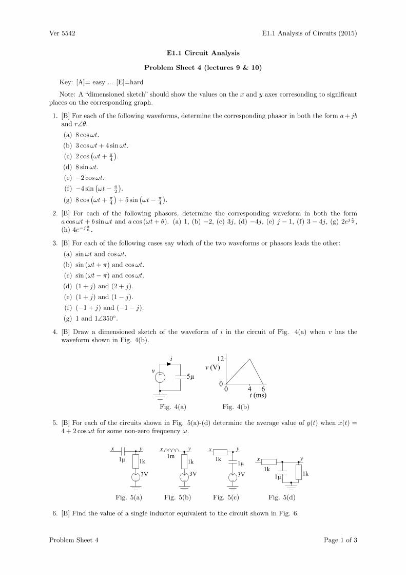
4. [B] Draw a dimensioned sketch of the waveform of i in the circuit of Fig. 4(a) when v has thewaveform shown in Fig. 4(b).
Fig. 4(a) Fig. 4(b)
5. [B] For each of the circuits shown in Fig. 5(a)-(d) determine the average value of y(t) when x(t) =4 + 2 cosωt for some non-zero frequency ω.
Fig. 5(a) Fig. 5(b) Fig. 5(c) Fig. 5(d)
6. [B] Find the value of a single inductor equivalent to the circuit shown in Fig. 6.
Problem Sheet 4 Page 1 of 3
Ver 5542 E1.1 Analysis of Circuits (2015)
Fig. 6 Fig. 7
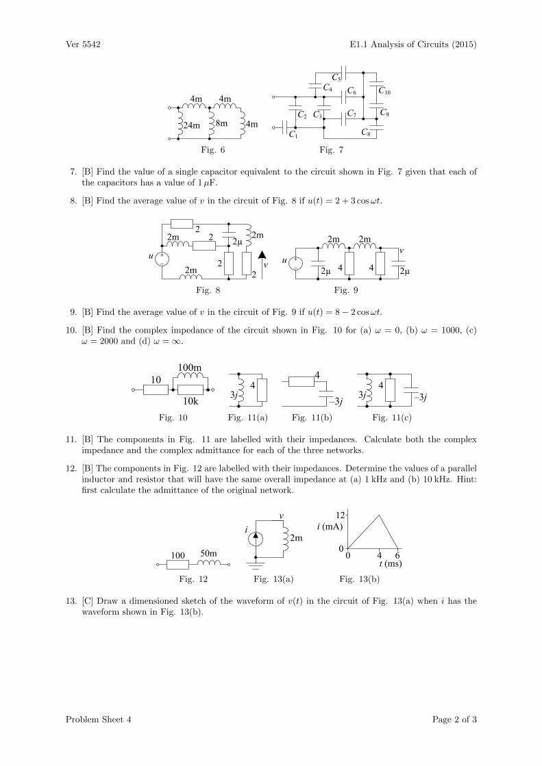
7. [B] Find the value of a single capacitor equivalent to the circuit shown in Fig. 7 given that each ofthe capacitors has a value of 1µF.
8. [B] Find the average value of v in the circuit of Fig. 8 if u(t) = 2 + 3 cosωt.
Fig. 8 Fig. 9
9. [B] Find the average value of v in the circuit of Fig. 9 if u(t) = 8− 2 cosωt.
10. [B] Find the complex impedance of the circuit shown in Fig. 10 for (a) ω = 0, (b) ω = 1000, (c)ω = 2000 and (d) ω =∞.
Fig. 10 Fig. 11(a) Fig. 11(b) Fig. 11(c)
11. [B] The components in Fig. 11 are labelled with their impedances. Calculate both the compleximpedance and the complex admittance for each of the three networks.
12. [B] The components in Fig. 12 are labelled with their impedances. Determine the values of a parallelinductor and resistor that will have the same overall impedance at (a) 1 kHz and (b) 10 kHz. Hint:first calculate the admittance of the original network.
Fig. 12 Fig. 13(a) Fig. 13(b)
13. [C] Draw a dimensioned sketch of the waveform of v(t) in the circuit of Fig. 13(a) when i has thewaveform shown in Fig. 13(b).
Problem Sheet 4 Page 2 of 3
Ver 5542 E1.1 Analysis of Circuits (2015)
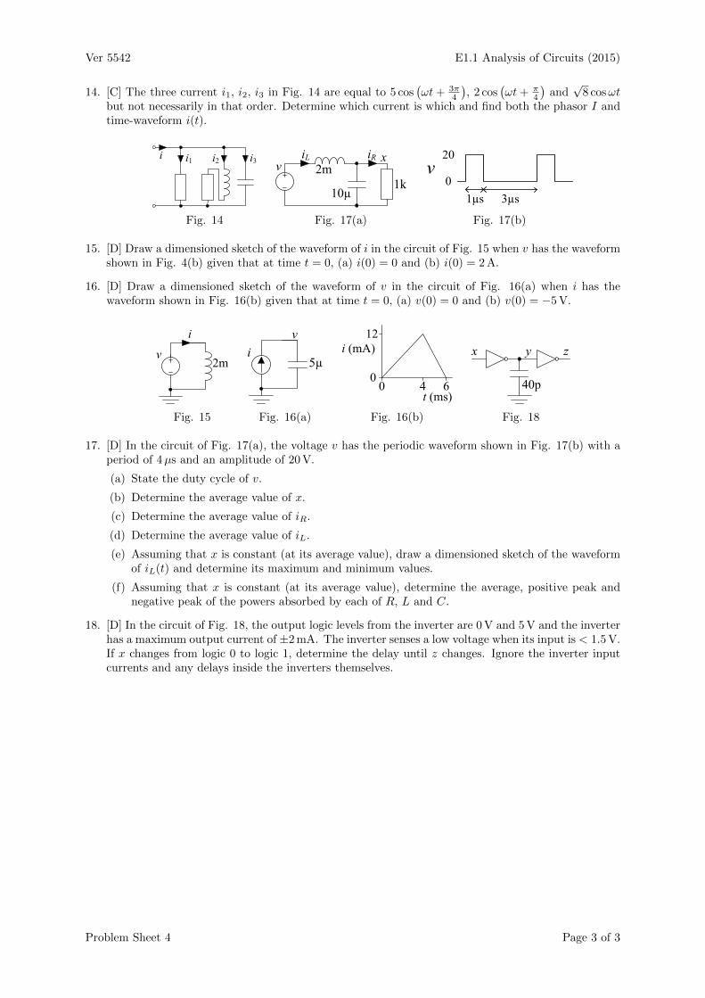
14. [C] The three current i1, i2, i3 in Fig. 14 are equal to 5 cos(ωt+ 3π
4
), 2 cos
(ωt+ π
4
)and√
8 cosωtbut not necessarily in that order. Determine which current is which and find both the phasor I andtime-waveform i(t).
Fig. 14 Fig. 17(a) Fig. 17(b)
15. [D] Draw a dimensioned sketch of the waveform of i in the circuit of Fig. 15 when v has the waveformshown in Fig. 4(b) given that at time t = 0, (a) i(0) = 0 and (b) i(0) = 2 A.
16. [D] Draw a dimensioned sketch of the waveform of v in the circuit of Fig. 16(a) when i has thewaveform shown in Fig. 16(b) given that at time t = 0, (a) v(0) = 0 and (b) v(0) = −5 V.
Fig. 15 Fig. 16(a) Fig. 16(b) Fig. 18
17. [D] In the circuit of Fig. 17(a), the voltage v has the periodic waveform shown in Fig. 17(b) with aperiod of 4µs and an amplitude of 20 V.
(a) State the duty cycle of v.
(b) Determine the average value of x.
(c) Determine the average value of iR.
(d) Determine the average value of iL.
(e) Assuming that x is constant (at its average value), draw a dimensioned sketch of the waveformof iL(t) and determine its maximum and minimum values.
(f) Assuming that x is constant (at its average value), determine the average, positive peak andnegative peak of the powers absorbed by each of R, L and C.
18. [D] In the circuit of Fig. 18, the output logic levels from the inverter are 0 V and 5 V and the inverterhas a maximum output current of ±2 mA. The inverter senses a low voltage when its input is < 1.5 V.If x changes from logic 0 to logic 1, determine the delay until z changes. Ignore the inverter inputcurrents and any delays inside the inverters themselves.
Problem Sheet 4 Page 3 of 3
Ver 10340 E1.1 Analysis of Circuits (2018)
E1.1 Circuit Analysis
Problem Sheet 4 - Solutions
1. (a) 8, (b) 3 − j4 = 5∠ − 0.93 (−53), (c) 1.4 + j1.4 = 2∠0.79 (45), (d) −j8 = 8∠ − 1.57 (90),(e) −2 = 2∠3.14 (180), (f) 4, (g) 2.12 + j2.12 = 3∠0.79 (45).
2. (a) cosωt, (b) −2 cosωt = 2 cos (ωt+ π), (c) −3 sinωt = 3 cos(ωt+ π
2
), (d) 4 sinωt = 4 cos
(ωt− π
2
),
(e) − cosωt − sinωt = 1.4 cos(ωt+ 3π
4
), (f) 3 cosωt + 4 sinωt = 5 cos (ωt− 0.93), (g) −2 sinωt =
2 cos(ωt+ π
2
), (h) 3.46 cosωt+ 2 sinωt = 4 cos
(ωt− π
6
).
3. (a) cosωt by π2 , (b) sin (ωt+ π) by π
2 , (c) sin (ωt− π) by π2 : note that sin (ωt+ π) and sin (ωt− π) are
actually the same waveform, (d) (1 + j) by 0.322 rad, (e) (1 + j) by π2 , (f) (−1− j) by π
2 , (g) 1 by 10.Because angles are only defined to within a multiple of 360, you always need to be careful whencomparing them. To find out which is leading, you need to take the difference in phase angles andthen add or subtract multiples of 360 to put the answer into the range ±180. Note that a sinewave is defined for all values of t (not just for t > 0) and so there is no such thing as the “first peak”of a sine wave.
4. i = C dvdt . dv
dt is 3000 V/s for the first 4 ms and −6000 V/s for the next 2 ms. So i = +15 or −30 mA.(see Fig. 4)
0 2 4 6-40
-20
0
20
t (ms)
i C (
mA
)
Fig. 4
5. The average value of x(t) is X = 4 (note that we use capital letters for quantities that do notvary with time). For averages (or equivalently for DC or ω = 0) capacitors act as open circuit andinductors as short circuits; this gives the simplified circuits shown below. So this gives (a) Y = 3,(b) Y = X = 4, (c) Y = X = 4, (d) Y = 1
2X = 2.
1k
X Y
3V4V
1k
X Y
3V4V
1k
X Y
3V4V1k
X Y
1k4V
Fig. 5(a) Fig. 5(b) Fig. 5(c) Fig. 5(d)
6. 4 + 4 = 8. 8||8 = 4. 4 + 4 = 8. 24||8 = 6 mH.
7. C9 and C10 are short-circuted and play no part in the circuit. We can merge series and parallelcapacitors as follows: C4,5 = 0.5, C7,8 = 2, C2,3 = 2. Now merge C4,5with C6 to give C4,5,6 =1.5 and merge this with C7,8 = 2 to give C4,5,6,7,8 = 6
7 . Now merge this with C2,3 = 2 to giveC2,3,4,5,6,7,8 = 20
7 . Finally merge this with C1 = 1 to give C = 2027 µF.
8. To determine average values, we can treat C as open circuit and L as short circuit. The originalcircuit simplifies to that shown in Fig. 8. So we have a simple potential divider and v = 1
2 u = 1 Vwhere the overbar denotes “average value”.
u
22
22v u
4
v
4
Fig. 8 Fig. 9
Solution Sheet 4 Page 1 of 3
Ver 10340 E1.1 Analysis of Circuits (2018)
9. To determine average values, we can treat C as open circuit and L as short circuit. The originalcircuit simplifies to that shown in Fig. 9 and so v = u = 8 V where the overbar denotes “averagevalue”.
10. Z = RS + RP ||jωL. (a) Z = RS = 10, (b) Z = 10 + 10000||100j = 11 + 100j = 100.6∠83.7,(c) Z = 10 + 10000||200j = 14 + 200j = 200.4∠86, (d) Z = 10010.
11. We denote the impedance by Z and the admittance by Y = 1Z . (a) Z = 1.44 + 1.92j and Y =
0.25 − 0.33j, (b) Z = 4 − 3j and Y = 0.16 + 0.12j, (c) Z = 4 and Y = 0.25. Notice that theimaginary part of the impedance (the reactance) is positive for inductive circuits and negative forcapacitive circuits, but that the imaginary part of the admittance (the susceptance) has the oppositesign. In part (c), the impedances of the inductor and the capacitor have cancelled out leavingan overall impedance that is purely real; because the impedances are frequency dependent, thiscancellation will only happen at one particular frequency which is called the network’s “resonantfrequency”. I strongly advise you to learn how to do these complex arithmetic manipulations usingthe built-in capabilities of the Casio fx-991.
12. (a) ω = 6283 so the impedance is Z = 100 + 314j. Taking the reciprocal gives Y = 1Z = 0.92 −
2.89jmS. Since parallel admittances add, the parallel component values must be RP = 10000.92 = 1087Ω
and LP = 10002.89ω = 55.1 mH. For case (b), we now have ω = 62832 and, following the same argument,
we get RP = 98.8 kΩ and LP = 50.05 mH. As the frequency goes up, the series resistor becomes aless significant part of the total impedance and its effect becomes less. This means that LP becomesapproximately equal to the original inductance and RP becomes larger.
13. v = L didt . didt is 3 A/s for the first 4 ms and −6 A/s for the next 2 ms. So v = +6 or −12 mV. (see
Fig. 13)
14. If we define the voltage phase to be φ will be ∠i1 = φ + 0, φ − π2 < ∠i2 < φ + 0, ∠i3 = φ + π
2 asthe CIVIL mnemonic reminds us. Thus i3 will have the most positive phase shift. It follows thati1 = 2 cos
(ωt+ π
4
), i2 =
√8 cosωt and i3 = 5 cos
(ωt+ 3π
4
)and that φ = π
4 . As phasors theseare I1 = 1.4 + j1.4 = 2∠45, I2 = 2.8, I3 = −3.5 + j3.5 = 5∠135. Adding these together givesI = 0.71 + j4.95 = 5∠1.43 (82). So i(t) = 0.71 cosωt− 4.95 sinωt = 5 cos (ωt+ 1.43) A.
15. i(t) = i(0) + 1L
´ tτ=0
v(τ)dτ where v(τ) = 3000τ for 0 ≤ τ ≤ 4 ms and v(τ) = 36 − 6000τ for4 ms ≤ τ ≤ 6 ms (obtain this formula by finding the straight line equalling 12 at τ = 4 ms and 0 atτ = 6 ms). So, for the first segment, i = 1
L × 1500t2 which reaches 12 A at t = 0.004. For the secondsegment, i = 1
L ×(36t− 3000t2
)+ c. To find c, we force i = 12 at t = 0.004. This gives c = −36 A.
When t = 0.006 we then get i = 18 A. For part (b), we just add 2 A to the curve. (see Fig. 15)
16. v = 1C
´idt where i = 3t or i = 36×10−3−6t. So, for the first segment, v = 1
C ×1.5t2 which reaches4.8 V at t = 0.004. For the second segment, v = 1
C ×(36× 10−3t− 3t2
)+ a. To find a, we force
v = 4.8 at t = 0.004. This gives a = −14.4 V. When t = 0.006 we then get v(t) = 7.2 V. For part(b), we just subtract 5 V from the curve. (see Fig. 16)
0 2 4 60
10
20
30
t (ms)
i-L (
A)
0 2 4 6-5
0
5
10
t (ms)
v C (
A)
0 2 4 6-20
-10
0
10
t (ms)
v L (
mV
)
Fig. 15 Fig. 16 Fig. 13
17. (a) The duty cycle is 0.25 = 25%, (b) Since the average voltage across an inductor is always zero,x = v = 1
4×20 = 5 V (where an overbar denotes the time-average), (c) iR = xR = 5 mA, (d) Since the
average current through a capacitor is always zero, iC = 0, and, from KCL, iL = iR = 5 mA, (e) Thevoltage across the inductor is v − x = LdiLdt . So when v = 20, diLdt = 20−5
L = 7.5 kA/s. So the totalchange in iL over the 1µs interval is 7.5 kA/s × 1µs = 7.5 mA. Similarly, during the 3µs interval,diLdt = 0−5
L = −2.5 kA/s, so the total change in iL over the 3µs interval is −2.5 kA/s×3µs = −7.5 mA.It follows that iLvaries from its average value of 5 mAby ±3.75 mAand has minimum and maximumvalues of 1.25 and 8.75 mA (see Fig. 17(a)). An alternative way to see this is to assume the theinitial value of iL equals C at the start of the 1µs interval and so the value at the end of the 1µs
Solution Sheet 4 Page 2 of 3

Ver 10340 E1.1 Analysis of Circuits (2018)
interval will be C + 7.5 and the average value during this interval will be iL = C + 3.75. Since weknow iL = iR = 5 mA, it follows that C = 5− 3.75 = 1.25 mA. (f) Average powers are PR = 25 mW,PL = PC = 0. Max powers are PR = 25 mW, PL = vLiL = 15 × 8.75 = 131.25 mW, PC = vCiC =5× 3.75 = 18.75 mW. Min powers are PR = 25 mW, PL = vLiL = −5× 8.75 = −43.75 mW (see Fig.17(b)), PC = vCiC = 5×−3.75 = −18.75 mW (see Fig. 17(c)). Note that during the time that it ispositive (0.5 < t < 2.5 ms), the average value of iC is ıC = 1.375 mA and so the total rise in vC willbe ∆vC = ıC∆t
C = 1.375×210 = 275 mV (i.e. ±138mVaround its mean) which is small compared to its
mean value of 5 V; this justifies the assumption that it is constant.
0 2 4 6 80
5
10
t (µs)
iL (
mA
)
0 2 4 6 8
0
50
100
t (µs)
PL
(mW
)
0 2 4 6 8-20
0
20
t (µs)
PC
(m
W)
Fig. 17(a) Fig. 17(b) Fig. 17(c)
18. When x changes from low to high, y will change from high to low. The maximum current is 2 mAso dy
dt = − iC = −50 MV/s. So the time to fall from 5 V to 1.5 V is 3.5
50 × 10−6 = 70 ns.
Solution Sheet 4 Page 3 of 3
Ver 10342 E1.1 Analysis of Circuits (2018)
E1.1 Circuit Analysis
Problem Sheet 5 (Lectures 11, 12 & 13)
Key: [A]= easy ... [E]=hard
Note: A “sketch” should show the values on the x and y axes corresonding to significant places onthe corresponding graph.
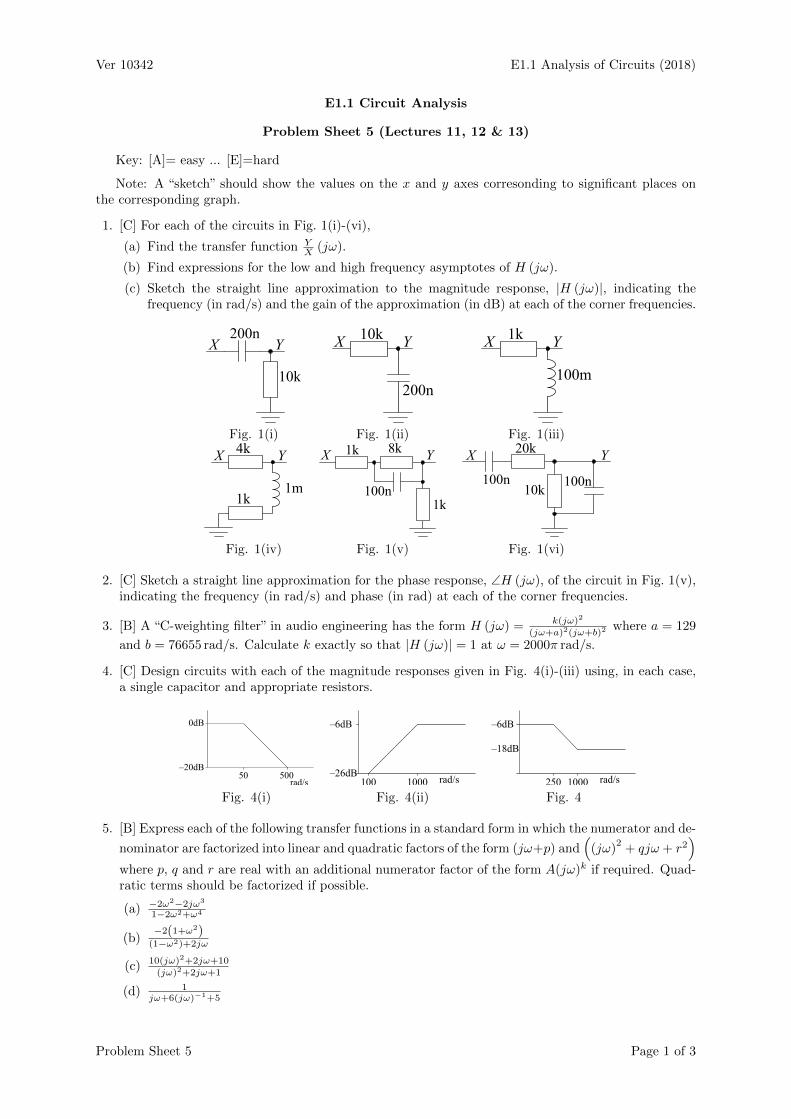
1. [C] For each of the circuits in Fig. 1(i)-(vi),
(a) Find the transfer function YX (jω).
(b) Find expressions for the low and high frequency asymptotes of H (jω).
(c) Sketch the straight line approximation to the magnitude response, |H (jω)|, indicating thefrequency (in rad/s) and the gain of the approximation (in dB) at each of the corner frequencies.
200n
10k
X Y
200n
10kX Y
100m
X Y1k
Fig. 1(i) Fig. 1(ii) Fig. 1(iii)
1m
X Y4k
1k
X Y8k
100n1k
1k X Y
100n10k
20k
100n
Fig. 1(iv) Fig. 1(v) Fig. 1(vi)
2. [C] Sketch a straight line approximation for the phase response, ∠H (jω), of the circuit in Fig. 1(v),indicating the frequency (in rad/s) and phase (in rad) at each of the corner frequencies.
3. [B] A “C-weighting filter” in audio engineering has the form H (jω) = k(jω)2
(jω+a)2(jω+b)2where a = 129
and b = 76655 rad/s. Calculate k exactly so that |H (jω)| = 1 at ω = 2000π rad/s.
4. [C] Design circuits with each of the magnitude responses given in Fig. 4(i)-(iii) using, in each case,a single capacitor and appropriate resistors.
0dB
–20dB50 500
rad/s
–6dB
–26dB100 1000 rad/s
–6dB
–18dB
250 1000 rad/s
Fig. 4(i) Fig. 4(ii) Fig. 4
5. [B] Express each of the following transfer functions in a standard form in which the numerator and de-
nominator are factorized into linear and quadratic factors of the form (jω+p) and(
(jω)2
+ qjω + r2)
where p, q and r are real with an additional numerator factor of the form A(jω)k if required. Quad-ratic terms should be factorized if possible.
(a) −2ω2−2jω3
1−2ω2+ω4
(b)−2(1+ω2)
(1−ω2)+2jω
(c) 10(jω)2+2jω+10
(jω)2+2jω+1
(d) 1jω+6(jω)−1+5
Problem Sheet 5 Page 1 of 3
Ver 10342 E1.1 Analysis of Circuits (2018)
6. [B] Without doing any algebra, determine the low and high frequency asymptotes of the followingtransfer functions:
(a) −2ω2−2jω3
1+ω4
(b) 2(jω)3+34(jω)4+1
(c)jω(2(jω)6+3)(5(jω)3+4jω+3)
2((jω)5+1)((jω)5+5)
(d) 12jω+6(jω)−1
7. [D] A circuit has a transfer function whose low and high frequency asymptotes are A (jω)α
and
B (jω)β
respectively. What constraints can you place on α and β if you know that the magnitude ofthe transfer function is less than G at all frequencies where G is a fixed real-valued constant.
8. [C] For each of the following transfer functions, sketch the straight line approximation to the mag-
nitude response and determine the gain of this approximation at ω = 1000 rad/s: (a) 5(1+jω/500)(1+jω/100)(1+jω/2000) ,
(b) 2(1+jω/5000)(1+jω/100) , (c) 3jω(1+jω/500)
(1+jω/100)(1+jω/2000)(1+jω/5000) .
9. [C] The frequency response of the circuit in Fig. 9 is given by( jω
p )2
( jωp )
2+2ζ( jω
p )+1where the corner
frquency, p = 1ζRC rad/s. Using capacitors of value C = 10 nF, design a filter with ζ =
√0.5 and a
corner frequency of p2π = 1 kHz. Determine the value of the transfer function at ω
2π = 100 Hz, 1 kHzand 10 kHz.
CX C
R
Z
ζ 2R
C1X
R1
ZC2
R2
10n 10n120k
3k
1 2 5 10 20 50 100 200-40
-30
-20
-10
0
10
Frequency (krad/s)
Gai
n (d
B)
A B C
Fig. 9 Fig. 11(a) Fig. 11(b)
10. [D] A high-pass “Butterworth” filter of order 2N consists of N cascaded copies of Fig. 9 all havingthe same corner frequency, but with the kth stage having ζk = cos
((2k−14N
)π)
where k = 1, . . . , N .(“cascaded” means you connect the output of one stage to the input of the next). Design a 4th orderhigh-pass Butterworth filter with a corner frequency of 1 kHz. Write an expression for its transferfunction and sketch its magnitude response using just the high and low asymptotes. Butterworthfilters are widely used because they have a very smooth magnitude response without any peaks; the
transfer function satisfies |H(jω)|2 =(ω
p )4N
(ωp )
4N+1
.
11. [C] The circuit of Fig. 11(a) is a high-pass filter whose magnitude response is marked“A”in Fig. 11(b). Using the filter transformations described in lectures, design filters with the magnitude responsesmarked “B” and “C” on the graph. Relative to “A”, these are respectively shifted up in frequency bya factor of 5 and reflected in the axis ω = 10, 000.
12. [C] (a) Find the resonant frequency, ωr, at which the impedance of the network in Fig. 12(i) is real.(b) Determine the Q of the circuit at ωr. (c) Find RP and LP in the circuit of Fig. 12(ii) so thatthe two networks have the same impedance at ωr.
10m1µ
10RS
C LS
1µ
C LP RP1µ
C10m
1kV
Fig. 12(i) Fig. 12(ii) Fig. 13
Problem Sheet 5 Page 2 of 3
Ver 10342 E1.1 Analysis of Circuits (2018)
13. [C] In the circuit of Fig. 13, ω = 10 000 and the phasor V = 10. Find (a) the peak power suppliedby V and (b) the peak power absorbed by C.
14. [C] Determine the transfer function for each of the circuits Fig. 14(i)-(iv).
X
Y
R 2R
C
XY
R 2R
C
Fig. 14(i) Fig. 14(ii)
XY
R 2R
C
C
4R X YR
C
RR
RR
RZ
Fig. 14(iii) Fig. 14(iv)
15. [D] For the circuit in Fig. 15,
(a) Find the transfer function ZW (jω) and explain why this is equal to Y
W (jω)
(b) Hence, by applying KCL at node W and using part (a) to substitute for W , show that thetransfer function Y
X (jω) = 1R1R2C1C2(jω)
2+(R1+R2)C1jω+1.
(c) From the transfer function expression we can express the corner frequency and damping factor
as p2 = 1R1R2C1C2
and ζ = p(R1+R2)C1
2 . By eliminating p between these equations, show that(1 + R2
R1
)(1 +
√1− C1
ζ2C2
)= 2. Explain why this means that we must choose C1 ≤ ζ2C2.
(d) Assuming that you only have available capacitors of values 10 nF, 22 nF and 47 nF, design afilter with p = 1000× 2π and ζ = 0.5. Choose C1 and C2 first. then R2
R1and lastly R1.
16. [D] For the circuit of Fig. 16,
(a) Find the transfer function YX (jω).
(b) Find the frequency, ω0, at which∣∣ YX (jω)
∣∣ is maximum and its value at this maximum.
(c) Find the 3dB bandwidth of the circuit and the value of Q = 12ζ .
[Note: If you find yourself doing loads of algebra, you are using the wrong method.]
X YR1 R2 Z
C1
C2W X Y20
80
100m 400n
Fig. 15 Fig. 16
Problem Sheet 5 Page 3 of 3
Ver 10342 E1.1 Analysis of Circuits (2018)
E1.1 Circuit Analysis
Problem Sheet 5 - Solutions
1. Each of the circuits may be viewed as a potential divider, so we can write down the transfer functionwithout doing any nodal analysis. In two cases, one element of the potential divider consists of a par-allel R||C combination. This parallel combination has the impedance 1
1/R+jωC = R1+jωRC . Graphs of
the magnitude responses are shown in Fig. 1(i)-(vi) together with their straight-line approximations.
(i) YX = R
R+1/jωC= jωRC
1+jωRC =jω/500
1+jω/500 where RC = 2 ms. LF asymptote is 0.002jω; HF asymptote
is 1. Denominator corner frequency is 1RC = 500 rad/s. At the corner, the gain is 1 = 0 dB.
(ii) YX =
1/jωC
R+1/jωC= 1
1+jωRC = 11+jω/500 where RC = 2 ms. LF asymptote is 1; HF asymptote is
500 (jω)−1
. Denominator corner frequency is 1RC = 500 rad/s. At the corner, the gain is 1 = 0 dB.
(iii) YX = jωL
R+jωL = jωL/R1+jωL/R where L
R = 100µs. LF asymptote is 10−4jω; HF asymptote is 1.
Denominator corner frequency is RL = 104 rad/s. At the corner, the gain is 1 = 0 dB.
(iv) For convenience, we define R = 1 k. Then YX = R+jωL
5R+jωL = 0.21+jω L
R
1+jω L5R
where LR = 1µs. LF
asymptote is 0.2; HF asymptote is 1. Numerator corner frequency is RL = 10 krad/s with a gain at
the corner of 0.2 = −14 dB. Denominator corner frequency is 5RL = 50 krad/s with a gain at the
corner of 1 = 0 dB. As can be seen in Fig. 1(iv), the magnitude response turns up at 10 krad/s and
then flattens out again at 50 krad/s . In between these two frequencies the slope log|H|logω = +1 or,
equivalently, +6 dB/octave or +20 dB/decade ; all these are the same as saying that |H| ∝ ω; thusfrom ω = 10 krad/s to 50 krad/s, the frequency increases by a factor of 5 and the gain also increasesby a factor of 5.
(v) For convenience, we define R = 1 k. Then YX = R
2R+ 8R1+8jωRC
= 1+8jωRC10+16jωRC = 0.1 1+8jωRC
1+1.6jωRC
where RC = 100µs. LF asymptote is 0.1; HF asymptote is 0.5. Numerator corner frequency is1
8RC = 1250 rad/s with a gain at the corner of 0.1 = −20 dB. Denominator corner frequency is1
1.6RC = 6.25 krad/s with a gain at the corner of 0.5 = −6 dB. As in the previous part, both thefrequency and the gain change by a factor of 5 between the corner frequencies.
(vi) For convenience, we defineR = 10 k. Then YX =
R1+jωRC
2R+ 1jωC + R
1+jωRC
= jωRC2jωRC(1+jωRC)+(1+jωRC)+jωRC =
jωRC1+4jωRC+2(jωRC)2
where RC = 1 ms. LF asymptote is 0.001jω; HF asymptote is 500 (jω)−1
. We
can factorize the denominator to give 1 + 4jωRC + 2 (jωRC)2
=(1 + jω
a
) (1 + jω
b
)where a and
b are −1 times the roots of the quadratic equation 2R2C2x2 + 4RCx + 1 or 1±√0.5
RC . This givesdenominator corner frequencies a = 293 and b = 1707 rad/s. The gain in between these two fre-quencies can be obtained by substituting ω = a into the LF asymptote expression to give a value ofaRC = 1−
√0.5 = 0.293 = −10.7 dB.
102
103
-20
-15
-10
-5
0
ω (rad/s)
|H| (
dB)
102
103
-20
-15
-10
-5
0
ω (rad/s)
|H| (
dB)
103
104
105
-20
-15
-10
-5
0
ω (rad/s)
|H| (
dB)
Fig. 1(i) Fig. 1(ii) Fig. 1(iii)
105
106
107
-25
-20
-15
-10
-5
0
ω (rad/s)
|H| (
dB)
103
104
-30
-25
-20
-15
-10
-5
ω (rad/s)
|H| (
dB)
102
103
104
-20
-15
-10
ω (rad/s)
|H| (
dB)
Fig. 1(iv) Fig. 1(v) Fig. 1(vi)
Solution Sheet 5 Page 1 of 7
Ver 10342 E1.1 Analysis of Circuits (2018)
2. For convenience, we define R = 1 k. Then YX = R
2R+ 8R1+8jωRC
= 1+8jωRC10+16jωRC = 0.1 1+8jωRC
1+1.6jωRC where
RC = 100µs. LF asymptote is 0.1; HF asymptote is 0.5; both of these are real and so havezero phase shift. The magnitude plot has a numerator corner frequency of 1
8RC = 1250 rad/sand denominator corner frequency of 1
1.6RC = 6.25 krad/s . Each of these generates a pair ofcorner frequencies on the phase plot at 0.1× and 10× the frequency. Thus we have corners atω = 125 (+), 625 (−), 12.5 k (−), 62.5 k (+) rad/s where the sign in parentheses indicates the gradi-ent change ±π4 rad/decade. Between 125 and 625 rad/s the gradient is π
4 rad/decade so the phasewill change by π
4 × log10625125 = π
4 × 0.7 = +0.55 rad. This is therefore the phase shift for the flat partof the phase response. (see Fig. 2).
103
104
0
0.2
0.4
0.6
0.8
ω (rad/s)
arg(
H)
(rad
)
102
103
104
105
-40
-30
-20
-10
0
ω (rad/s)
|H| (
dB)
Fig. 2 Fig. 3
3. At ω = 2000π = 6283.2 we know |H(jω)| = 1. Hence k = |jω+a|2|jω+b|2
|jω|2 =(ω2+a2)(ω2+b2)
ω2 =
3.9495×107×5.9155×1093.9478×107 = 5.918× 10⁹.
4. (i) This is the same low-pass filter as Fig. 1(ii) but with a corner frequency of 50 rad/s. So we wantRC = 1
50 = 20 ms. One possible choice is shown in Fig. 4(i).
(ii) This is the same high-pass filter as Fig. 1(i) but with a corner frequency of 1000 rad/s and a highfrequency gain of 0.5 = −6 dB. So we want RC = 1
1000 = 1 ms. One possible choice is shown in Fig.4(ii); the two resistors give the correct high frequency gain.
(iii) We want a circuit whose gain decreases from 12 at low frequencies to 1
8 at high frequencies. Wecan do this by using a capacitor to short out part of the vertical limb of the potential divider athigh frequencies as shown in Fig. 4(iii). This design has a gain of 1
8 when the capacitor is a shortcircuit; with the capacitor open circuit (low frequencies), we add in an additional 6R which gives a
gain of 12 . The impedance of 6R||C is
R+ 6R1+6jωRC
8R+ 6R1+6jωRC
= 7+6jωRC14+48jωRC which, as a check, we see has the
correct LF and HF asymptotes. The numerator corner frequency is at ω = 76RC which needs to be
at 1000 rad/s. From this, RC = 1.17 ms so one possible set of value is C = 100 nF and R = 12 kΩ.
500n
40kX Y 100n
5k
X Y5k X Y7R
C6R
R
Fig. 4(i) Fig. 4(ii) Fig. 4
5. (a) −2ω2−2jω3
1−2ω2+ω4 = 2(jω)2(jω+1)
((jω)2+1)((jω)2+1).
(b)−2(1+ω2)
(1−ω2)+2jω = 2(jω+1)(jω−1)(jω+1)(jω+1) = 2(jω−1)
(jω+1)
(c) 10(jω)2+2jω+10
(jω)2+2jω+1=
10((jω)2+0.2jω+1)(jω+1)(jω+1)
(d) 1jω+6(jω)−1+5
= jω(jω)2+5jω+6
= jω(jω+2)(jω+3)
Solution Sheet 5 Page 2 of 7

Ver 10342 E1.1 Analysis of Circuits (2018)
6. To find the low frequency asymptote, you take the lowest power of jω in each of the numerator anddenominator factors and multiply them together. Likewise, for the high frequency asymptote, youtake the highest power of jω in each of the factors. There is no need (or indeed advantage) to doany factorization or to multiply out existing factors.
(a) HLF = −2ω2
1 = 2(jω)2, HHF = −2jω3
ω4 = 2(jω)−1
(b) HLF = 31 = 3, HHF = 2(jω)3
4(jω)4 = 0.5(jω)−1
(c) HLF = jω×3×32×1×5 = 0.9jω, HHF = jω×2(jω)6×5(jω)3
2×(jω)5×(jω)5 = 5
(d) HLF = 126(jω)−1 = 2jω, HHF = 12
jω = 12(jω)−1
7. We must have α ≥ 0 because, if α were negative, (jω)α
would increase without limit as ω → 0and the transfer function would exceed G at some point. Similarly, we must have β ≤ 0 becauseotherwise (jω)βwould increase without limit as ω → ∞. A consequence of this is that the order ofthe numerator can never exceed that of the denominator in a transfer function whose magnitude isbounded.
8. Graphs of the transfer functions are shown in Fig. 8(a)-(c).
(a) We have a LF asymptote of 5 = 14 dB. We have corner frequencies at ω = 100 (−), 500 (+), 2000 (−)where the sign in parentheses indicates the polarity of gradient change. To estimate the gain atω = 1000, we assume that a factor
∣∣1 + jωa
∣∣ is equal to 1 if ω < a or else ωa if ω > a. This gives
|H(1000j)| '∣∣∣ 5(ω/500)(ω/100)(1)
∣∣∣ = 1 = 0 dB.
(b) We have a LF asymptote of 2 = 6 dB. We have corner frequencies at ω = 100 (−), 5000 (+).
Using the same technique as in part (a), |H(1000j)| '∣∣∣ 2(1)(ω/100)
∣∣∣ =∣∣ 2001000
∣∣ = 0.2 = −14 dB.
(c) We have corner frequencies at ω = 100 (−), 500 (+), 2000 (−), 5000 (−). We have a LF asymptoteof 3jω = 6 dB which at the first corner (ω = 100) is 300j = 50 dB. Using the same technique as in
part (a), |H(1000j)| '∣∣∣ 3×ω(ω/500)(ω/100)(1)(1)
∣∣∣ =∣∣ 3000
5
∣∣ = 600 = 55.6 dB. To obtain this expression from the
transfer function, any term whose corner frequency is > ω has been replaced by (1).
101 102 103 104
(rad/s)
-20
-10
0
10
|H|(
dB)
101 102 103 104
(rad/s)
-20
-10
0
|H|(
dB)
101 102 103 104
(rad/s)
30
40
50
60
|H|(
dB)
Fig. 8(a) Fig. 8(b) Fig. 8(c)
9. The corner frequency is p = 1ζRC = 2π × 1000. Rearranging this gives R = 1
2000πζC = 22508 Ω.
The upper resistor therefore has a value ζ2R = 0.5R = 11254 Ω. The complete circuit is shown inFig. 9. At ω = 100 Hz, 1 kHz and 10 kHz the value of jω
p = 0.1j, j and 10j respectively. From the
question, the transfer function is given by( jω
p )2
( jωp )
2+2ζ( jω
p )+1. Substituting for jω
p and ζ =√
0.5, this
equals −0.01−0.01+0.1414j+1 = −0.0099 + 0.0014j = 0.01∠172, −1
−1+1.414j+1 = 0.707j = 0.707∠90 and−100
−100+14.14j+1 = 0.9899 + 0.1414j = 1∠8 respectively.
10n
X
22.5k
Z
10n
11.25k
10n
X
17.2k10n
14.7k
10n41.6k
Z
10n
6.1k
Y
100 200 500 1k 2k 5k 10k
-80
-60
-40
-20
0
Frequency (Hz)
|H| (
dB)
Fig. 9 Fig. 10(a) Fig. 10(b)
Solution Sheet 5 Page 3 of 7

Ver 10342 E1.1 Analysis of Circuits (2018)
10. For a 4th order filter, we need N = 2 and from the formula given in the question, we use ζ1 =cos(π8
)= 0.924 and ζ2 = cos
(3π8
)= 0.383. If we stick to C = 10 nF as in Q9, we obtain R1 =
12000πζ1C
= 17.2 kΩ and R2 = 12000πζ2C
= 41.6 kΩ with ζ21R1 = 14.7 kΩ and ζ22R2 = 6.1 kΩ. This gives
the circuit shown in Fig. 10(a). The transfer function isH(jω) =( jω
p )4(
( jωP )
2+2ζ1( jω
p )+1)(
( jωP )
2+2ζ2( jω
p )+1)
; this is plotted in Fig. 10(b).
11. To shift the frequency response up by a factor of 5, we need to divide the value of each C or Lcomponent by 5. This gives the circuit of Fig. 11(a). We could also, if we wanted, multiply all thecapacitor values by k and divide all the resistor values by k for any scale factor k without changingthe transfer function. For this particular circuit, it would be a bad idea to use a value of k > 1because, at 3 kΩ the feedback resistor is already a little on the low side for many op-amps (whichhave a limited current output capability).
To reflect the magnitude response in the line ωm = 10000, we need to convert resistors into capacitorsand vice-versa. From the notes, the formulae are: R′ = k
ωmC, C ′ = 1
ωmkR. For the circuit of
Fig. 11(b), I have chosen k = 3.33 in order to get reasonable component values but other choices arealso possible. A full analysis of this low-pass filter circuit is the subject of question 15.
C1X
R1
ZC2
R2
2n 2n120k
3k
X R1 ZR2
C1
C2
250p
10n
33k 33k
Fig. 11(a) Fig. 11(b)
12. (a) The parallel combination of C||(R+ L) has an impedance Z =1
jωC (R+jωL)1
jωC +R+jωL= R+jωL
1+jωRC+(jω)2LC.
We want to find the value of ω that makes this real. The easiest way to do this is to insist that theratio of imaginary to real part is the same for the numerator and denominator (this implies that theyhave the same argument). Thus ωrL
R = ωrRC1−ω2
rLCfrom which cross multiplying (after dividing both
numerators by ωr) gives L−ω2rL
2C = R2C from which ωr =√
L−R2CL2C = 9 950 rad/s. Note that this
is close, but not exactly equal to, ω0 = 10 000 where the capacitor and inductor impedances havethe same magnitude. The value of Z at resonance can now be found as the ratio between the real(or equivalently the imaginary) parts of the numerator and denominator of the previous expression.Thus Z = R+jωL
1+jωRC+(jω)2LC= R
1−ω2LC = jωLjωRC = 1000.
(b) By definition Q equals ωr times the average stored energy divided by the average power loss. If
the input voltage phasor is V , then the peak energy stored in the capacitor is 12C |V |
2and its average
stored energy is half this, namely 14C |V |
2. The current through the resistor is IR = V
R+jωrL. The
peak energy stored in the inductor is 12L |IR|
2= 1
2L|V |2
R2+ω2rL
2 = 12L
|V |2
R2+L−R2C
L2CL2
= 12L
C|V |2R2C+L−R2C =
12C |V |
2which is the same as the peak capacitor energy; likewise, the average energy stored in the
inductor is 14C |V |
2. The average power loss in the resistor is 1
2R |IR|2
= RC2L |V |
2. Calculating Q
from its definition gives Q = ωr14C|V |
2+ 14C|V |
2
RC2L |V |
2 = ωrLR = 9.95. Since the capacitor and inductor store
the same amount of energy on average, the Q can be determined more simply as Q = ωr12L|IR|
2
12R|IR|
2 =ωrLR = 9.95 .
(c) Note that the capacitor is unchanged in the two networks, so we can ignore it when matchingtheir impedances. When choosing components to make two networks have the same impedance,your have a choice: you can either match their impedances or their admittances. You get the sameanswer in either case, but the algebra can sometimes be much simpler in one case than the other.In this question, it is easiest to use admittances because the components whose values are unknownare in parallel and so their admittances add: the total admittance of RP and LP in parallel is1RP− j
ωrLPand RP and LP remain unentangled in this expression. The admittance of RS + LS is
Solution Sheet 5 Page 4 of 7
Ver 10342 E1.1 Analysis of Circuits (2018)
1RS+jωrLS
= RS−jωrLS
R2S+ω2
rL2S
= 1RP− j
ωrLP. Equating the real and imaginary parts of this equation gives,
RP =R2
S+ω2rL
2S
RS= 1 kΩ and LP =
R2S+ω2
rL2S
ω2rLS
= LS + R2
ω2rLS
= 10.1 mH.
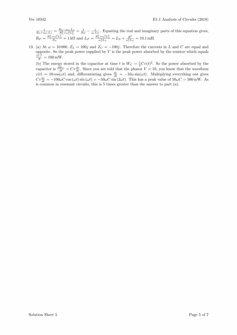
13. (a) At ω = 10 000, ZL = 100j and ZC = −100j. Therefore the currents in L and C are equal andopposite. So the peak power supplied by V is the peak power absorbed by the resistor which equals|V |2R = 100 mW.
(b) The energy stored in the capacitor at time t is WC = 12Cv(t)2. So the power absorbed by the
capacitor is dWC
dt = Cv dvdt . Since you are told that the phasor V = 10, you know that the waveform
v(t) = 10 cos(ωt) and, differentiating gives dvdt = −10ω sin(ωt). Multiplying everything out gives
Cv dvdt = −100ωC cos (ωt) sin (ωt) = −50ωC sin (2ωt). This has a peak value of 50ωC = 500 mW. Asis common in resonant circuits, this is 5 times greater than the answer to part (a).
Solution Sheet 5 Page 5 of 7
Ver 10342 E1.1 Analysis of Circuits (2018)
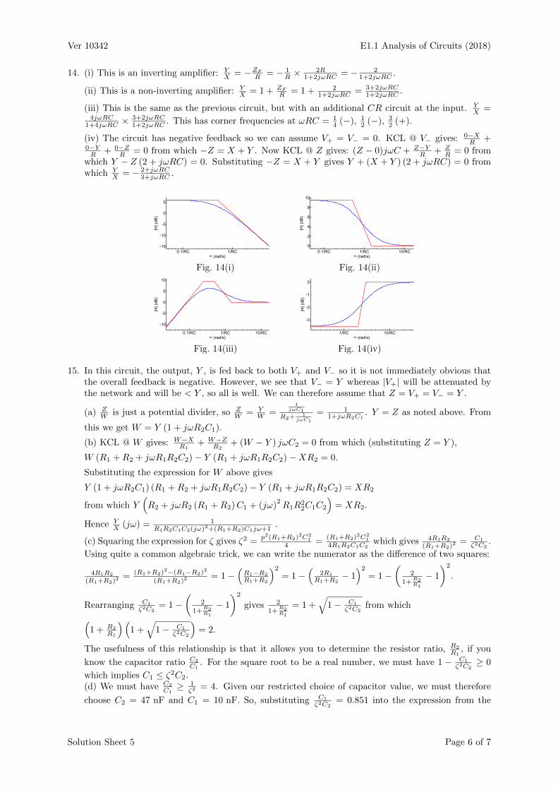
14. (i) This is an inverting amplifier: YX = −ZF
R = − 1R ×
2R1+2jωRC = − 2
1+2jωRC .
(ii) This is a non-inverting amplifier: YX = 1 + ZF
R = 1 + 21+2jωRC = 3+2jωRC
1+2jωRC .
(iii) This is the same as the previous circuit, but with an additional CR circuit at the input. YX =
4jωRC1+4jωRC ×
3+2jωRC1+2jωRC . This has corner frequencies at ωRC = 1
4 (−), 12 (−), 3
2 (+).
(iv) The circuit has negative feedback so we can assume V+ = V− = 0. KCL @ V− gives: 0−XR +
0−YR + 0−Z
R = 0 from which −Z = X + Y . Now KCL @ Z gives: (Z − 0)jωC + Z−YR + Z
R = 0 fromwhich Y − Z (2 + jωRC) = 0. Substituting −Z = X + Y gives Y + (X + Y ) (2 + jωRC) = 0 fromwhich Y
X = − 2+jωRC3+jωRC .
0.1/RC 1/RC-15
-10
-5
0
5
ω (rad/s)
|H| (
dB)
0.1/RC 1/RC 10/RC0
2
4
6
8
10
ω (rad/s)
|H| (
dB)
Fig. 14(i) Fig. 14(ii)
0.1/RC 1/RC 10/RC
-10
-5
0
5
10
ω (rad/s)
|H| (
dB)
1/RC 10/RC
-3
-2
-1
0
ω (rad/s)
|H| (
dB)
Fig. 14(iii) Fig. 14(iv)
15. In this circuit, the output, Y , is fed back to both V+ and V− so it is not immediately obvious thatthe overall feedback is negative. However, we see that V− = Y whereas |V+| will be attenuated bythe network and will be < Y , so all is well. We can therefore assume that Z = V+ = V− = Y .
(a) ZW is just a potential divider, so Z
W = YW =
1jωC1
R2+1
jωC1
= 11+jωR2C1
. Y = Z as noted above. From
this we get W = Y (1 + jωR2C1).
(b) KCL @ W gives: W−XR1
+ W−ZR2
+ (W − Y ) jωC2 = 0 from which (substituting Z = Y ),
W (R1 +R2 + jωR1R2C2)− Y (R1 + jωR1R2C2)−XR2 = 0.
Substituting the expression for W above gives
Y (1 + jωR2C1) (R1 +R2 + jωR1R2C2)− Y (R1 + jωR1R2C2) = XR2
from which Y(R2 + jωR2 (R1 +R2)C1 + (jω)
2R1R
22C1C2
)= XR2.
Hence YX (jω) = 1
R1R2C1C2(jω)2+(R1+R2)C1jω+1
.
(c) Squaring the expression for ζ gives ζ2 =p2(R1+R2)
2C21
4 =(R1+R2)
2C21
4R1R2C1C2which gives 4R1R2
(R1+R2)2 = C1
ζ2C2.
Using quite a common algebraic trick, we can write the numerator as the difference of two squares:
4R1R2
(R1+R2)2 = (R1+R2)
2−(R1−R2)2
(R1+R2)2 = 1−
(R1−R2
R1+R2
)2= 1−
(2R1
R1+R2− 1)2
= 1−(
2
1+R2R1
− 1
)2
.
Rearranging C1
ζ2C2= 1−
(2
1+R2R1
− 1
)2
gives 2
1+R2R1
= 1 +√
1− C1
ζ2C2from which(
1 + R2
R1
)(1 +
√1− C1
ζ2C2
)= 2.
The usefulness of this relationship is that it allows you to determine the resistor ratio, R2
R1, if you
know the capacitor ratio C2
C1. For the square root to be a real number, we must have 1 − C1
ζ2C2≥ 0
which implies C1 ≤ ζ2C2.(d) We must have C2
C1≥ 1
ζ2 = 4. Given our restricted choice of capacitor value, we must therefore
choose C2 = 47 nF and C1 = 10 nF. So, substituting C1
ζ2C2= 0.851 into the expression from the
Solution Sheet 5 Page 6 of 7
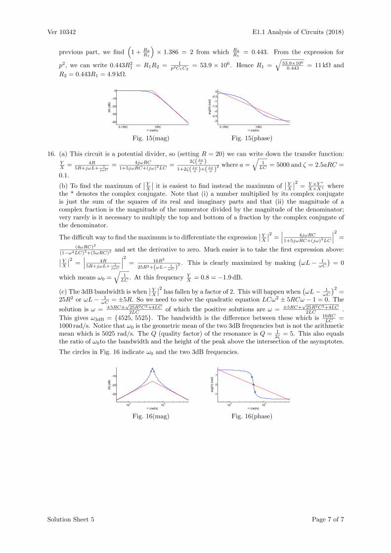
Ver 10342 E1.1 Analysis of Circuits (2018)
previous part, we find(
1 + R2
R1
)× 1.386 = 2 from which R2
R1= 0.443. From the expression for
p2, we can write 0.443R21 = R1R2 = 1
p2C1C2= 53.9 × 10⁶. Hence R1 =
√53.9×10⁶
0.443 = 11 kΩ and
R2 = 0.443R1 = 4.9 kΩ.
0.1/RC 1/RC
-40
-30
-20
-10
0
ω (rad/s)
|H| (
dB)
0.1/RC 1/RC
-3
-2.5
-2
-1.5
-1
-0.5
0
ω (rad/s)
arg(
H)
(rad
)
Fig. 15(mag) Fig. 15(phase)
16. (a) This circuit is a potential divider, so (setting R = 20) we can write down the transfer function:
YX = 4R
5R+jωL+ 1jωC
= 4jωRC1+5jωRC+(jω)2LC
=2ζ( jω
a )1+2ζ( jω
a )+( jωa )
2 where a =√
1LC = 5000 and ζ = 2.5aRC =
0.1.
(b) To find the maximum of∣∣ YX
∣∣ it is easiest to find instead the maximum of∣∣ YX
∣∣2 = Y×Y ∗
X×X∗ wherethe * denotes the complex conjugate. Note that (i) a number multiplied by its complex conjugateis just the sum of the squares of its real and imaginary parts and that (ii) the magnitude of acomplex fraction is the magnitude of the numerator divided by the magnitude of the denominator;very rarely is it necessary to multiply the top and bottom of a fraction by the complex conjugate ofthe denominator.
The difficult way to find the maximum is to differentiate the expression∣∣ YX
∣∣2 =∣∣∣ 4jωRC1+5jωRC+(jω)2LC
∣∣∣2 =
(4ωRC)2
(1−ω2LC)2+(5ωRC)2and set the derivative to zero. Much easier is to take the first expression above:∣∣ Y
X
∣∣2 =∣∣∣ 4R5R+jωL+ 1
jωC
∣∣∣2 = 16R2
25R2+(ωL− 1ωC )
2 . This is clearly maximized by making(ωL− 1
ωC
)= 0
which means ω0 =√
1LC . At this frequency Y
X = 0.8 = −1.9 dB.
(c) The 3dB bandwidth is when∣∣ YX
∣∣2 has fallen by a factor of 2. This will happen when(ωL− 1
ωC
)2=
25R2 or ωL− 1ωC = ±5R. So we need to solve the quadratic equation LCω2 ± 5RCω − 1 = 0. The
solution is ω = ±5RC±√25R2C2+4LC2LC of which the positive solutions are ω = ±5RC+
√25R2C2+4LC2LC .
This gives ω3dB = 4525, 5525. The bandwidth is the difference between these which is 10RCLC =
1000 rad/s. Notice that ω0 is the geometric mean of the two 3dB frequencies but is not the arithmeticmean which is 5025 rad/s. The Q (quality factor) of the resonance is Q = 1
2ζ = 5. This also equalsthe ratio of ω0to the bandwidth and the height of the peak above the intersection of the asymptotes.
The circles in Fig. 16 indicate ω0 and the two 3dB frequencies.
103
104
-30
-20
-10
ω (rad/s)
|H| (
dB)
103
104
-1
0
1
ω (rad/s)
arg(
H)
(rad
)
Fig. 16(mag) Fig. 16(phase)
Solution Sheet 5 Page 7 of 7
Ver 8954 E1.1 Analysis of Circuits (2016)
E1.1 Circuit Analysis
Problem Sheet 6 (Lectures 14, 15 & 16)
Key: [A]= easy ... [E]=hard
Note: A tilde-superscript on a phasor denotes division by√
2, i.e. V = 1√2V . This means that
∣∣∣V ∣∣∣equals the RMS value of a phasor V .
1. [A] Say which of the following waveforms include negative exponentials and which include positiveexponentials: (a) 2− 4e−3t, (b) 2 + 4e3t, (c) 2 + 4e−3t, (d) −2− 4e3t, (e) 2 + 4e−t/−3.
2. [B] Suppose v(t) = 5 + 2e−100t.
(a) Determine the time constant, τ , of the negative exponential.
(b) Determine the time at which v(t) = 5.5 V.
(c) Give an expression for the time taken for v(t) to fall from A to B where 5 < B < A < 7.
3. [B] If V = −200j in Fig. 3, find the phasor value of I and the complex power absorbed by each ofthe components including the voltage source.
4. [B] If v(t) =
0 t < 0
5 t ≥ 0in Fig. 4 (below),
(a) find an expression for x(t) for t ≥ 0.
(b) Sketch a graph of x(t) for −RC ≤ t ≤ 3RC.
(c) Determine the time at which x(t) = 4.5.
5. [C] For each of the circuits shown in Fig. 5(i)-(vi) determine (a) the time constant (b) the DC gainYX
∣∣ω=0
and (c) the high frequency gain YX
∣∣ω=∞. In each case, determine these in two ways: directly
from the circuit and via the transfer function.
Fig. 3 Fig. 5(i) Fig. 5(ii) Fig. 5(iii)
Fig. 4 Fig. 5(iv) Fig. 5(v) Fig. 5(vi)
6. [C] For each of the periodic waveforms shown in Fig. 6(i)-(iii) determine (a) the mean value and (b)the rms value.
0 1 2 3 4 5 6-2
0
2
4
6
0 1 2 3 4 5 60
1
2
3
4
0 1 2 3 4 5 60
2
4
6
Fig. 6(i) Fig. 6(ii) Fig. 6(iii)
Problem Sheet 6 Page 1 of 3
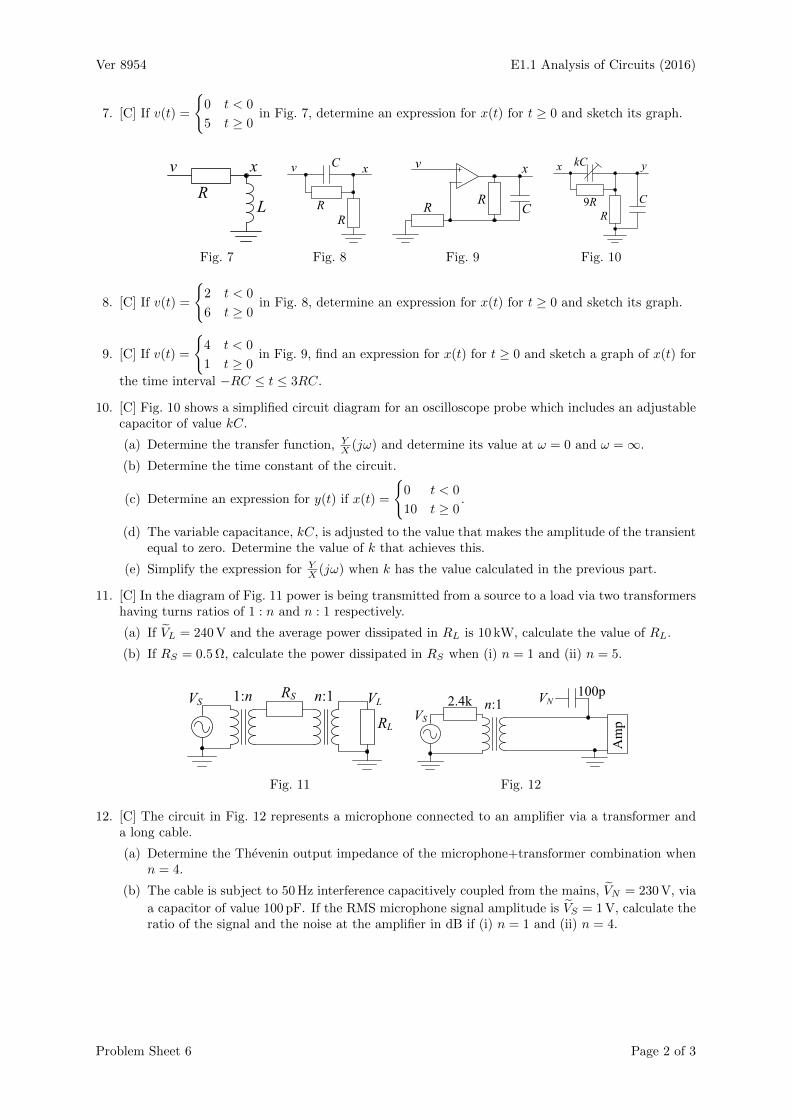
Ver 8954 E1.1 Analysis of Circuits (2016)
7. [C] If v(t) =
0 t < 0
5 t ≥ 0in Fig. 7, determine an expression for x(t) for t ≥ 0 and sketch its graph.
Fig. 7 Fig. 8 Fig. 9 Fig. 10
8. [C] If v(t) =
2 t < 0
6 t ≥ 0in Fig. 8, determine an expression for x(t) for t ≥ 0 and sketch its graph.
9. [C] If v(t) =
4 t < 0
1 t ≥ 0in Fig. 9, find an expression for x(t) for t ≥ 0 and sketch a graph of x(t) for
the time interval −RC ≤ t ≤ 3RC.
10. [C] Fig. 10 shows a simplified circuit diagram for an oscilloscope probe which includes an adjustablecapacitor of value kC.
(a) Determine the transfer function, YX (jω) and determine its value at ω = 0 and ω =∞.
(b) Determine the time constant of the circuit.
(c) Determine an expression for y(t) if x(t) =
0 t < 0
10 t ≥ 0.
(d) The variable capacitance, kC, is adjusted to the value that makes the amplitude of the transientequal to zero. Determine the value of k that achieves this.
(e) Simplify the expression for YX (jω) when k has the value calculated in the previous part.
11. [C] In the diagram of Fig. 11 power is being transmitted from a source to a load via two transformershaving turns ratios of 1 : n and n : 1 respectively.
(a) If VL = 240 V and the average power dissipated in RL is 10 kW, calculate the value of RL.
(b) If RS = 0.5 Ω, calculate the power dissipated in RS when (i) n = 1 and (ii) n = 5.
Fig. 11 Fig. 12
12. [C] The circuit in Fig. 12 represents a microphone connected to an amplifier via a transformer anda long cable.
(a) Determine the Thevenin output impedance of the microphone+transformer combination whenn = 4.
(b) The cable is subject to 50 Hz interference capacitively coupled from the mains, VN = 230 V, via
a capacitor of value 100 pF. If the RMS microphone signal amplitude is VS = 1 V, calculate theratio of the signal and the noise at the amplifier in dB if (i) n = 1 and (ii) n = 4.
Problem Sheet 6 Page 2 of 3
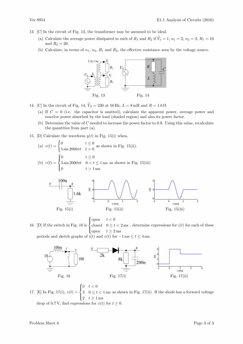
Ver 8954 E1.1 Analysis of Circuits (2016)
13. [C] In the circuit of Fig. 13, the transformer may be assumed to be ideal.
(a) Calculate the average power dissipated in each of R1 and R2 if Vs = 1, n1 = 2, n2 = 3, R1 = 10and R2 = 20.
(b) Calculate, in terms of n1, n2, R1 and R2, the effective resistance seen by the voltage source.
Fig. 13 Fig. 14
14. [C] In the circuit of Fig. 14, VS = 230 at 50 Hz, L = 8 mH and R = 1.6 Ω.
(a) If C = 0 (i.e. the capacitor is omitted), calculate the apparent power, average power andreactive power absorbed by the load (shaded region) and also its power factor.
(b) Determine the value of C needed to increase the power factor to 0.9. Using this value, recalculatethe quantities from part (a).
15. [D] Calculate the waveform y(t) in Fig. 15(i) when,
(a) v(t) =
0 t ≤ 0
5 sin 2000πt t > 0as shown in Fig. 15(ii).
(b) v(t) =
0 t ≤ 0
5 sin 2000πt 0 < t ≤ 1 ms
0 t > 1 ms
as shown in Fig. 15(iii)
-1 0 1 2-5
0
5
t (ms)-1 0 1 2
-5
0
5
t (ms)
Fig. 15(i) Fig. 15(ii) Fig. 15(iii)
16. [D] If the switch in Fig. 16 is
open t < 0
closed 0 ≤ t < 2 ms
open t ≥ 2 ms
, determine expressions for i(t) for each of these
periods and sketch graphs of i(t) and v(t) for −1 ms ≤ t ≤ 4 ms.
-1 0 1 2 3
0
1
2
3
t (ms)
Fig. 16 Fig. 17(i) Fig. 17(ii)
17. [E] In Fig. 17(i), v(t) =
0 t < 0
3 0 ≤ t < 1 ms
2 t ≥ 1 ms
as shown in Fig. 17(ii). If the diode has a forward voltage
drop of 0.7 V, find expressions for x(t) for t ≥ 0.
Problem Sheet 6 Page 3 of 3
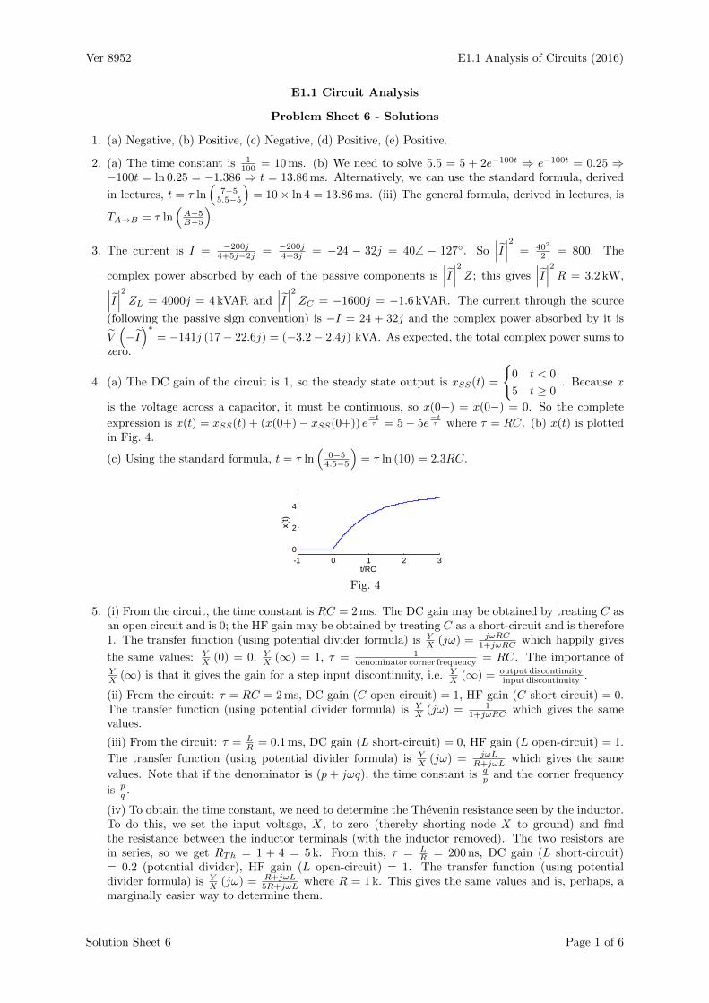
Ver 8952 E1.1 Analysis of Circuits (2016)
E1.1 Circuit Analysis
Problem Sheet 6 - Solutions
1. (a) Negative, (b) Positive, (c) Negative, (d) Positive, (e) Positive.
2. (a) The time constant is 1100 = 10 ms. (b) We need to solve 5.5 = 5 + 2e−100t ⇒ e−100t = 0.25 ⇒
−100t = ln 0.25 = −1.386 ⇒ t = 13.86 ms. Alternatively, we can use the standard formula, derived
in lectures, t = τ ln(
7−55.5−5
)= 10× ln 4 = 13.86 ms. (iii) The general formula, derived in lectures, is
TA→B = τ ln(A−5B−5
).
3. The current is I = −200j4+5j−2j = −200j
4+3j = −24 − 32j = 40∠ − 127. So∣∣∣I∣∣∣2 = 402
2 = 800. The
complex power absorbed by each of the passive components is∣∣∣I∣∣∣2 Z; this gives
∣∣∣I∣∣∣2R = 3.2 kW,∣∣∣I∣∣∣2 ZL = 4000j = 4 kVAR and∣∣∣I∣∣∣2 ZC = −1600j = −1.6 kVAR. The current through the source
(following the passive sign convention) is −I = 24 + 32j and the complex power absorbed by it is
V(−I)∗
= −141j (17− 22.6j) = (−3.2− 2.4j) kVA. As expected, the total complex power sums tozero.
4. (a) The DC gain of the circuit is 1, so the steady state output is xSS(t) =
0 t < 0
5 t ≥ 0. Because x
is the voltage across a capacitor, it must be continuous, so x(0+) = x(0−) = 0. So the complete
expression is x(t) = xSS(t) + (x(0+)− xSS(0+)) e−tτ = 5− 5e
−tτ where τ = RC. (b) x(t) is plotted
in Fig. 4.
(c) Using the standard formula, t = τ ln(
0−54.5−5
)= τ ln (10) = 2.3RC.
-1 0 1 2 30
2
4
t/RC
Fig. 4
5. (i) From the circuit, the time constant is RC = 2 ms. The DC gain may be obtained by treating C asan open circuit and is 0; the HF gain may be obtained by treating C as a short-circuit and is therefore1. The transfer function (using potential divider formula) is Y
X (jω) = jωRC1+jωRC which happily gives
the same values: YX (0) = 0, Y
X (∞) = 1, τ = 1denominator corner frequency = RC. The importance of
YX (∞) is that it gives the gain for a step input discontinuity, i.e. Y
X (∞) = output discontinuityinput discontinuity .
(ii) From the circuit: τ = RC = 2 ms, DC gain (C open-circuit) = 1, HF gain (C short-circuit) = 0.The transfer function (using potential divider formula) is Y
X (jω) = 11+jωRC which gives the same
values.
(iii) From the circuit: τ = LR = 0.1 ms, DC gain (L short-circuit) = 0, HF gain (L open-circuit) = 1.
The transfer function (using potential divider formula) is YX (jω) = jωL
R+jωL which gives the same
values. Note that if the denominator is (p+ jωq), the time constant is qp and the corner frequency
is pq .
(iv) To obtain the time constant, we need to determine the Thevenin resistance seen by the inductor.To do this, we set the input voltage, X, to zero (thereby shorting node X to ground) and findthe resistance between the inductor terminals (with the inductor removed). The two resistors arein series, so we get RTh = 1 + 4 = 5 k. From this, τ = L
R = 200 ns, DC gain (L short-circuit)= 0.2 (potential divider), HF gain (L open-circuit) = 1. The transfer function (using potentialdivider formula) is Y
X (jω) = R+jωL5R+jωL where R = 1 k. This gives the same values and is, perhaps, a
marginally easier way to determine them.
Solution Sheet 6 Page 1 of 6
Ver 8952 E1.1 Analysis of Circuits (2016)
(v) To determine the Thevenin resistance seen by the capacitor, we set X = 0 and measure theresistance at the capacitor terminals. Since X is connected to ground, the two 1 k resistors are inseries and so we have 8 k in parallel with 2 k which gives 1.6 k. From this, τ = RC = 0.16 ms, DC gain(C open-circuit) = 0.1 (potential divider), HF gain (C short-circuit) = 0.5. The transfer function(using potential divider formula) is Y
X (jω) = R2R+ 8R
1+8jωRC
= 1+8jωRC10+16jωRC where R = 1 k and we used
the formula for Z8R||C = 8R1+jω8RC .
(vi) To determine the Thevenin resistance at the capacitor terminals is not trivial because of thedependent voltage source that is the opamp. If we set X = 0 and replace the capacitor with a voltagesource V as in Fig. 5(i), we can use nodal analysis to determine I and then calculate RTh = V
I . Since
the op-amp is a unit-gain buffer, Y = V . KCL at node W gives: W10 + W−V
10 + W−V10 = 0 ⇒ W =
23V ⇒ I = V−W
10 ==13V
10 = V30 ⇒ RTh = 30 k. So, finally, we get τ = RThC = 3 ms. For the DC
gain, we make C an open-circuit as in Fig. 5(ii). Negative feedback means V+ = Y and, since thereis no current through the resistor connected to V+, we must also have W = Y . KCL at node Wthen gives W = Y = X, so the DC gain is 1. For the HF gain, the capacitor acts a a short circuitso V+ = 0 which in turn means that Y = 0 so the gain is 0.
Rather easier is the transfer function approach. We know V+ = Y and V+ is determined from W
by an RC potential divider giving: YW = V+
W = 11+jωRC . KCL at W gives W−X
R + W−YR + W−Y
R =
0 ⇒ 3W − 2Y = X. We now substitute for W using the previous equation YW = 1
1+jωRC to get
3Y (1 + jωRC) − 2Y = X⇒ YX = 1
1+3jωRC . From this we can easily get: τ = 3RC, YX (0) = 1 and
YX (∞) = 0.
-1 0 1 2 30
2
4
t*R/L
Fig. 5(i) Fig. 5(ii) Fig. 7
6. (i) v(t) equals 6 for 13 of the time and−2 for 2
3 of the time. So its average value is v = 13×6+2
3×(−2) =23 . Similarly, the average value of v2 is v2 = 1
3 × 36+23 × 4 = 142
3 . So Vrms =√
14.67 = 3.83. This ishigher than the average value v.
(ii) During the first period (0 ≤ t ≤ 2), the formula for v can be derived as v = 2t. To findthe average value, we integrate over one period, and divide by the length of the period. So v =12
∫ 2
t=02tdt = 1
2
[t2]20
= 2. This is also pretty obvious from looking at the waveform. In the same
way, v2 = 12
∫ 2
t=0(2t)
2dt = 1
2
[43 t
3]20
= 5 13 giving Vrms =
√5.33 = 2.31.
(iii) This is the same as the previous waveform but shifted up by +2. You can perform integrationssimilar to the previous part or, easier, just modify the previous answers. v (which previously equalled2) will be increased by 2 to become v = 4. Adding a constant onto a random variable does not affect
its variance, so v2 − (v)2
will be unchanged at 5 13 − 22 = 1 1
3 . It follows that v2 = (v)2
+ 113 = 17 1
3 .
Taking the square root gives Vrms =√
17.33 = 4.16.
7. Method 1 (inductor current continuity): For t < 0, x = 0 and the current through the inductoris i = v−x
R = 0. It follows that at time t = 0+, the current through the resistor (which equalsthe current through the inductor) will still be zero and x(0+) = v(0+) = 5. From this value iswill decay to a steady state value xSS = 0 since the inductor is a short circuit for DC. Thus,x(t) = xSS(t) + (x(0+)− xSS(0+)) e
−tτ = 0 + 5e
−tτ where τ = L
R . This is plotted in Fig. 7.
Method 2 (transfer function): The transfer function of the circuit is (from potential divider equation)XV = jωL
R+jωL . From this we get the DC gain, GDC = 0, the HF gain, GHF = 1, and the time constant
is LR . The DC gain allows us to calculate the steady state xSS(t) = GDCv(t) ≡ 0. The output
discontinuity at t = 0 is given by ∆x = GHF∆v = 1×5 = 5. So x(0+) = xSS(0−)+∆x = 0+5 = 5.
Finally we put everything together to get: x(t) = xSS(t)+(x(0+)− xSS(0+)) e−tτ = 0+(5− 0) e
−tτ .
Solution Sheet 6 Page 2 of 6
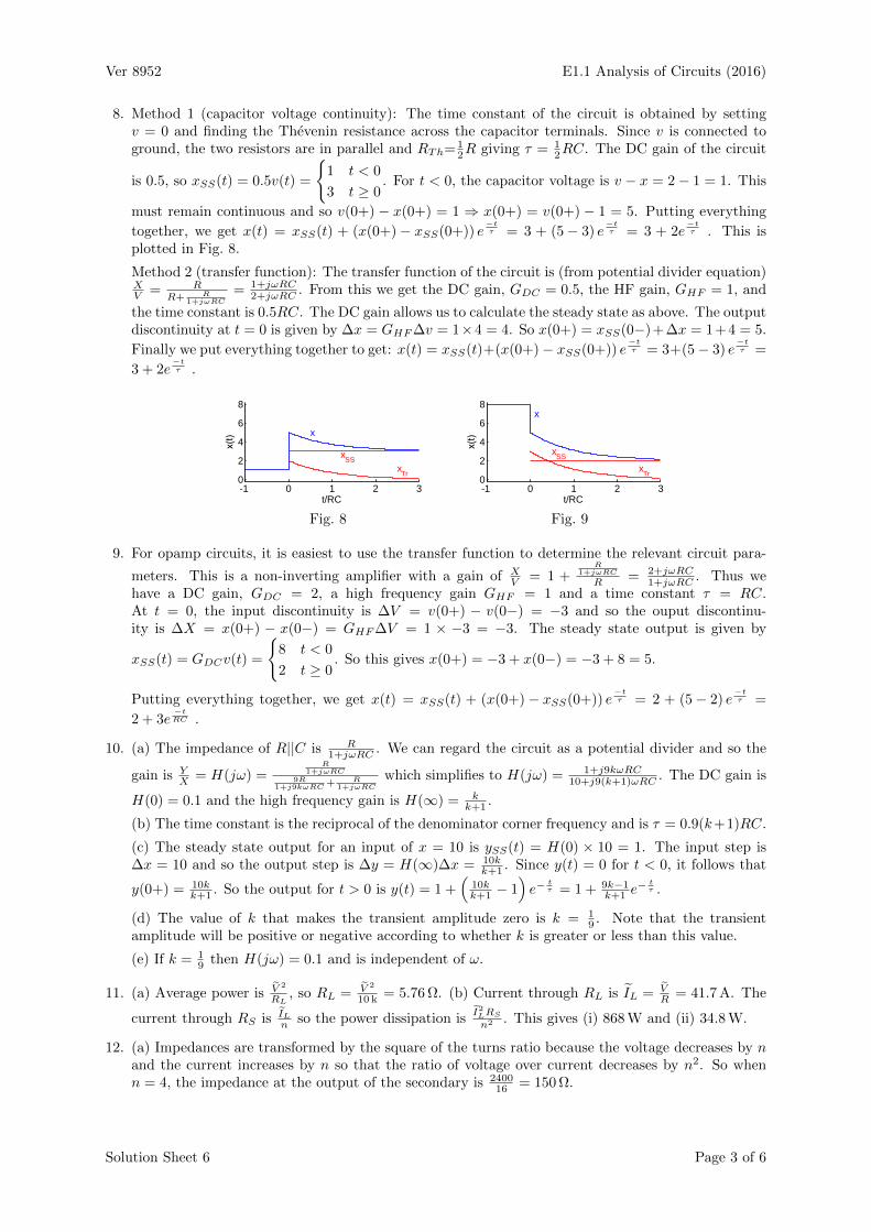
Ver 8952 E1.1 Analysis of Circuits (2016)
8. Method 1 (capacitor voltage continuity): The time constant of the circuit is obtained by settingv = 0 and finding the Thevenin resistance across the capacitor terminals. Since v is connected toground, the two resistors are in parallel and RTh=1
2R giving τ = 12RC. The DC gain of the circuit
is 0.5, so xSS(t) = 0.5v(t) =
1 t < 0
3 t ≥ 0. For t < 0, the capacitor voltage is v − x = 2− 1 = 1. This
must remain continuous and so v(0+) − x(0+) = 1 ⇒ x(0+) = v(0+) − 1 = 5. Putting everything
together, we get x(t) = xSS(t) + (x(0+)− xSS(0+)) e−tτ = 3 + (5− 3) e
−tτ = 3 + 2e
−tτ . This is
plotted in Fig. 8.
Method 2 (transfer function): The transfer function of the circuit is (from potential divider equation)XV = R
R+ R1+jωRC
= 1+jωRC2+jωRC . From this we get the DC gain, GDC = 0.5, the HF gain, GHF = 1, and
the time constant is 0.5RC. The DC gain allows us to calculate the steady state as above. The outputdiscontinuity at t = 0 is given by ∆x = GHF∆v = 1×4 = 4. So x(0+) = xSS(0−)+∆x = 1+4 = 5.
Finally we put everything together to get: x(t) = xSS(t)+(x(0+)− xSS(0+)) e−tτ = 3+(5− 3) e
−tτ =
3 + 2e−tτ .
-1 0 1 2 30
2
4
6
8
t/RC
xSS
xTr
x
-1 0 1 2 30
2
4
6
8
t/RC
xSS
xTr
x
Fig. 8 Fig. 9
9. For opamp circuits, it is easiest to use the transfer function to determine the relevant circuit para-
meters. This is a non-inverting amplifier with a gain of XV = 1 +
R1+jωRC
R = 2+jωRC1+jωRC . Thus we
have a DC gain, GDC = 2, a high frequency gain GHF = 1 and a time constant τ = RC.At t = 0, the input discontinuity is ∆V = v(0+) − v(0−) = −3 and so the ouput discontinu-ity is ∆X = x(0+) − x(0−) = GHF∆V = 1 × −3 = −3. The steady state output is given by
xSS(t) = GDCv(t) =
8 t < 0
2 t ≥ 0. So this gives x(0+) = −3 + x(0−) = −3 + 8 = 5.
Putting everything together, we get x(t) = xSS(t) + (x(0+)− xSS(0+)) e−tτ = 2 + (5− 2) e
−tτ =
2 + 3e−tRC .
10. (a) The impedance of R||C is R1+jωRC . We can regard the circuit as a potential divider and so the
gain is YX = H(jω) =
R1+jωRC
9R1+j9kωRC+ R
1+jωRC
which simplifies to H(jω) = 1+j9kωRC10+j9(k+1)ωRC . The DC gain is
H(0) = 0.1 and the high frequency gain is H(∞) = kk+1 .
(b) The time constant is the reciprocal of the denominator corner frequency and is τ = 0.9(k+1)RC.
(c) The steady state output for an input of x = 10 is ySS(t) = H(0) × 10 = 1. The input step is∆x = 10 and so the output step is ∆y = H(∞)∆x = 10k
k+1 . Since y(t) = 0 for t < 0, it follows that
y(0+) = 10kk+1 . So the output for t > 0 is y(t) = 1 +
(10kk+1 − 1
)e−
tτ = 1 + 9k−1
k+1 e− tτ .
(d) The value of k that makes the transient amplitude zero is k = 19 . Note that the transient
amplitude will be positive or negative according to whether k is greater or less than this value.
(e) If k = 19 then H(jω) = 0.1 and is independent of ω.
11. (a) Average power is V 2
RL, so RL = V 2
10 k = 5.76 Ω. (b) Current through RL is IL = VR = 41.7 A. The
current through RS is ILn so the power dissipation is
I2LRSn2 . This gives (i) 868 W and (ii) 34.8 W.
12. (a) Impedances are transformed by the square of the turns ratio because the voltage decreases by nand the current increases by n so that the ratio of voltage over current decreases by n2. So whenn = 4, the impedance at the output of the secondary is 2400
16 = 150 Ω.
Solution Sheet 6 Page 3 of 6

Ver 8952 E1.1 Analysis of Circuits (2016)
(b) At 50 Hz, the capacitor impedance is ZC = 1j2π50×100 p = −j31.8 MΩ . With the transformed
source impedance from part (a), we get the equivalent circuit shown in Fig. 12. Using superposition,
VA = VN× Rn−2
Rn−2+ZC+ VSn
−1 × ZCRn−2+ZC
= n−1ZC VS+Rn−2VN
Rn−2+ZC. The ratio of the signal and noise
voltages is equal to the ratio of the two terms in the numerator, so the ratio of the signal and noise
voltage magnitudes isn−1|ZC ||VS|Rn−2|VN | = 31.8M×1
2400×230 × n = 57.66 × n. Converting this to decibels gives
20 log10 57.66 + 20 log10 n = 35.2 + 20 log10 n. This gives (i) 35.2 dB for n = 1 and (ii) 47.3 dB forn = 4. So, slightly surprisingly, using a transfomer to reduce the voltage coming from the microphoneactually makes the signal-to-noise ratio better.
Fig. 12 Fig. 13
13. (a) V1 = n1VS = 2 so the average power dissipated in R1 isV 21
R1= 400 mW. Similarly, V2 = n2VS = 3,
so the average power dissipated in R2 isV 22
R2= 450 mW.
(b) From the ideal transformer equations, 1× IS +n1× (−I1)+n2× (−I2) = 0 (the minus signs arisebecause in Fig. 13 I1 and I2 are defined as coming out of the transformer). Rearranging this and
using Ohm’s law gives IS = n1I1+n2I2 = n1V1
R1+ n2V2
R2=
n21VSR1
+n22VSR2
. So Reff = VSIS
= 11
n−21 R1
+ 1
n−22 R2
.
This is the same as the parallel combination of n−21 R1 and n−22 R2 , i.e. the parallel combination ofthe individual winding resistances transferred from the secondaries to the primary.
14. (a) The inductor impedance is jωL = j × 100π × 0.008 = 2.51 Ω. So the current is I = VSR+jωL =
41.5−65.1j. So S = V I∗ = P+jQ = 9.54+14.98j kVA. So the apparent power is |S| = 17.8 kVAandthe average and reactive powers are P and Q given earlier. The power factor is cosφ = P
|S| = 0.54.
(b) Adding the capacitor will not consume any average power and so will not affect P at all. Weneed to reduce Q to P tan (arccos 0.9) = 4.62 kVAR since tanφ = Q
P and we want cosφ = 0.9. It
follows that QC = 4.62− 14.98 = −10.36 kVAR = −|VS |2|ZC | = −2302ωC. This gives C = 623µF. Now
S = P + jQ = 9.54 + 4.62j kVA. So the apparent power is |S| = 10.6 kVA and the average andreactive powers are P and Q given earlier. The power factor is cosφ = P
|S| = 0.9.
15. Notice first that since there are no input discontinuities, there will be no output discontinuitieseither. The circuit transfer function is X
V = jωRC1+jωRC . The gain at ω = 2000π is G = 0.503 +
0.5j = 0.709∠44.8. The phasor corresponding to v(t) = 5 sinωt is V = −5j and so the steadystate output will be X = GV = 2.5 − 2.51j = 3.54∠ − 45.2 which corresponds to a waveformxSS(t) = 2.5 cosωt+ 2.51 sinωt. The time constant is RC = 0.16 ms.
(a) At time t = 0+ we have xSS(0+) = 2.5 V. Since there is no output discontinuity, x(0+) =
x(0−) = 0. Putting this together gives x(t) = xSS(t) + (x(0+)− xSS(0+)) e−tτ = 2.5 cosωt +
2.51 sinωt+ (0− 2.5) e−tRC . This is plotted in Fig. 15(i).
(b) Substituting t = 1 into the previous expression gives x(1−) = x(1+) = 2.495 (very close to thesteady state value since it has had 6 1
4 time constants to converge). For t > 1, the steady state is
xSS(t) ≡ 0. Therefore we get x(t) = 2.495e−(t−1)τ . This is plotted in Fig. 15(ii).
Solution Sheet 6 Page 4 of 6

Ver 8952 E1.1 Analysis of Circuits (2016)
-1 0 1 2-5
0
5
t (ms)
xSS
xTr
x
-1 0 1 2-5
0
5
t (ms)
xSS
xTr x
Fig. 15(i) Fig. 15(ii)
16. For the steady state when t < 0, we can treat the inductor as a short circuit and so i = 10R = 100 mA.
When the switch is closed, there is a constant 10 V across the inductor and so didt = V
L = 100 V/s.Therefore the current through the inductor will increase linearly at this rate for 2 ms (from an initialvalue of 100 mA) and will reach a value of 300 mA. Since there is no resistor in series with theinductor, the current increases linearly rather than exponentially; you can, if you wish, regard thisas a limiting case of a negative exponential that has an infinite time constant.
When the switch is opened at t = 2 ms, the current will decay from its peak value of 300 mA backdown to its steady state value of 100 mA with a time constant of L
R = 1 ms. Thus for t > 2 ms, we
have i(t) = 100 + (300− 100) e−(t−2)
1 (in units of mA and ms). All this is plotted in Fig. 16(i).
When the switch is open, v(t) = Ri(t). However, when the switch is closed, v(t) ≡ 0. We thereforeget the voltage waveform plotted in Fig. 16(v).
-1 0 1 2 3 40
100
200
300
t (ms)
iSS
iTr
i
-1 0 1 2 3 40
10
20
30
t (ms)
vSS
v
Fig. 16(i) Fig. 16(v)
17. In this question, we have two different circuits according to whether the diode is off or on. These areshown in Fig. 17(off),(on). When the diode is off, we have a DC steady state xSS(t) = 0 and a timeconstant τOff = RC = 1.6 ms. On the other hand, when the diode is on, we can get the DC steadystate by doing KCL for the shaded supernode: x+0.7−v
2 + x8 = 0 ⇒ xSS = 4
5 (v − 0.7). We obtainthe time constant by setting all voltage sources to zero and finding the Thevenin resistance and thecapacitor terminals: this is RTh = 2 k||8 k = 1.6 k; this gives a time constant τOn = 0.32 ms.
For t < 0, v = x = 0 and so, since v− x < 0.7, the diode will be off. When v changes to 3, the diodewill turn on and will charge the capacitor up to a steady state voltage of 4
5 (3− 0.7) = 1.84. Whenv now changes to 2 V, the diode will turn off and x will fall towards the “off” steady state of 0 V.However, it will never reach this value, because when x reaches v − 0.7 = 1.3 V the diode will turnon again resulting in a new steady state of 4
5 (2− 0.7) = 1.04 V. So this means we actually have fourdistinct time segments: t < 0, 0 ≤ t < 1, 1 ≤ t < Tx, t ≥ Tx wher Tx is the, as yet unknown, timeat which the diode turns on for the last time.
Segment 1 (Diode Off, t < 0, x = v = 0).
Segment 2 (Diode On, 0 ≤ t < 1, v = 3, xSS = 45 (3− 0.7) = 1.84, τOn = 0.32 ms): x(t) =
xSS(t) + (x(0+)− xSS(0+)) e−tτ = 1.84 + (0− 1.84) e
−tτ = 1.84 − 1.84e
−tτOn . At t = 1 this gives
x(1) = 1.76.
Segment 3 (Diode Off, 1 ≤ t < Tx, v = 2, xSS = 0, τOff = 1.6 ms): Capacitor voltage continuity
means that x(1+) = 1.76. So x(t) = xSS(t) + (x(1+)− xSS(1+)) e−tτ = 0 + (1.76− 0) e
−tτ =
1.76e−(t−1)τOff . We need to know when the voltage x reaches 1.3 V (t = Tx) because that is when the
diode will turn on again. Solving 1.76e−(Tx−1)τOff = 1.3⇒ Tx = 1.48 ms.
Segment 4 (Diode On, t ≥ 1.48 ms, v = 2, xSS = 45 (2− 0.7) = 1.04, τOn = 0.32 ms): x(t) =
xSS(t) + (x(Tx+)− xSS(Tx+)) e−tτ = 1.04 + (1.3− 1.04) e
−tτ = 1.04 + 0.26e
−(t−Tx)τOn .
All four segments are plotted in Fig. 17(iii).
Solution Sheet 6 Page 5 of 6
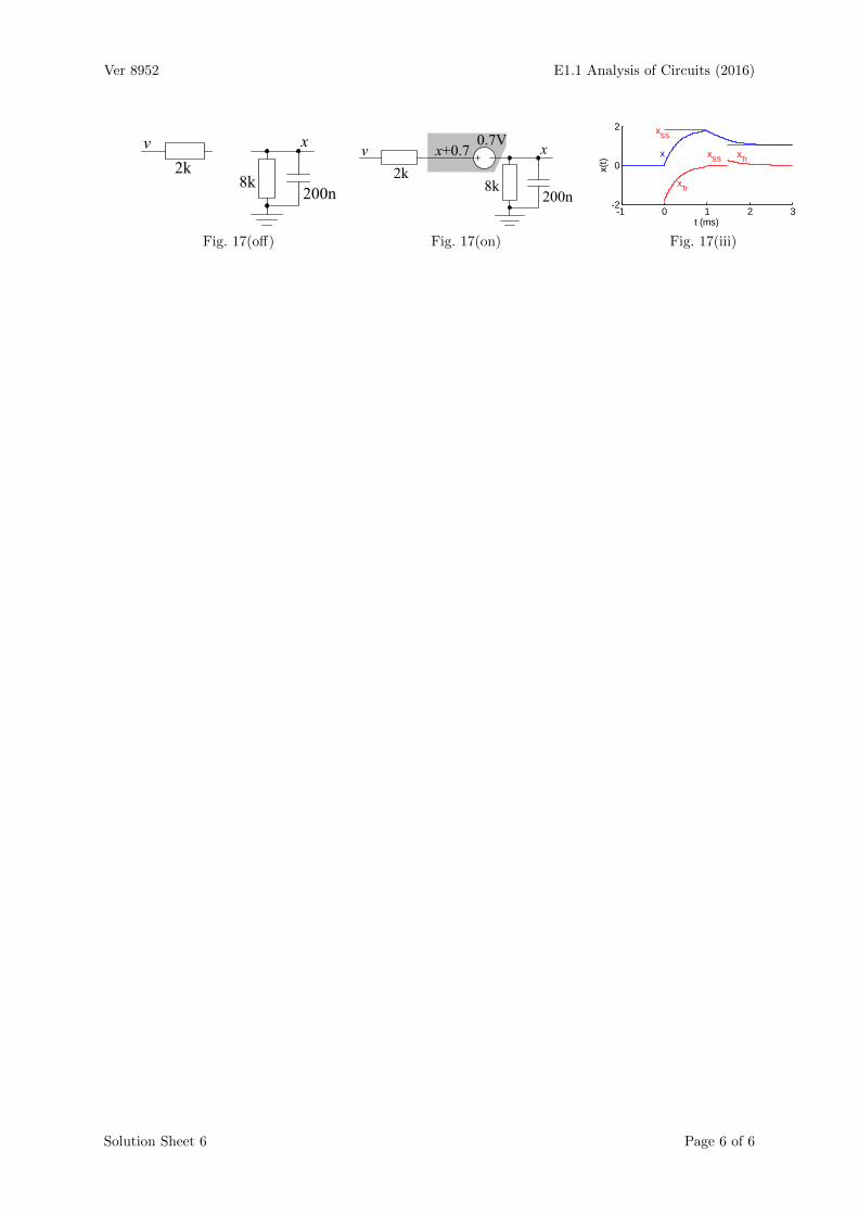
Ver 8952 E1.1 Analysis of Circuits (2016)
-1 0 1 2 3-2
0
2
t (ms)
xSS
xTr
x xSS
xTr
Fig. 17(off) Fig. 17(on) Fig. 17(iii)
Solution Sheet 6 Page 6 of 6
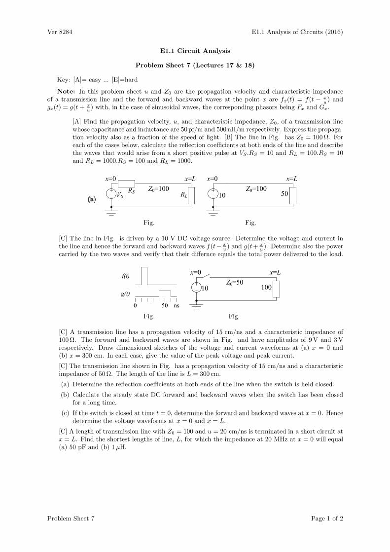
Ver 8284 E1.1 Analysis of Circuits (2016)
E1.1 Circuit Analysis
Problem Sheet 7 (Lectures 17 & 18)
Key: [A]= easy ... [E]=hard
Note: In this problem sheet u and Z0 are the propagation velocity and characteristic impedanceof a transmission line and the forward and backward waves at the point x are fx(t) = f(t − x
u ) andgx(t) = g(t+ x
u ) with, in the case of sinusoidal waves, the corresponding phasors being Fx and Gx.
[A] Find the propagation velocity, u, and characteristic impedance, Z0, of a transmission linewhose capacitance and inductance are 50 pf/m and 500 nH/m respectively. Express the propaga-tion velocity also as a fraction of the speed of light. [B] The line in Fig. has Z0 = 100 Ω. Foreach of the cases below, calculate the reflection coefficients at both ends of the line and describethe waves that would arise from a short positive pulse at VS .RS = 10 and RL = 100.RS = 10and RL = 1000.RS = 100 and RL = 1000.
(a)(b)(c)
Fig. Fig.
[C] The line in Fig. is driven by a 10 V DC voltage source. Determine the voltage and current inthe line and hence the forward and backward waves f(t− x
u ) and g(t+ xu ). Determine also the power
carried by the two waves and verify that their differnce equals the total power delivered to the load.
Fig. Fig.
[C] A transmission line has a propagation velocity of 15 cm/ns and a characteristic impedance of100 Ω. The forward and backward waves are shown in Fig. and have amplitudes of 9 V and 3 Vrespectively. Draw dimensioned sketches of the voltage and current waveforms at (a) x = 0 and(b) x = 300 cm. In each case, give the value of the peak voltage and peak current.
[C] The transmission line shown in Fig. has a propagation velocity of 15 cm/ns and a characteristicimpedance of 50 Ω. The length of the line is L = 300 cm.
(a) Determine the reflection coefficients at both ends of the line when the switch is held closed.
(b) Calculate the steady state DC forward and backward waves when the switch has been closedfor a long time.
(c) If the switch is closed at time t = 0, determine the forward and backward waves at x = 0. Hencedetermine the voltage waveforms at x = 0 and x = L.
[C] A length of transmission line with Z0 = 100 and u = 20 cm/ns is terminated in a short circuit atx = L. Find the shortest lengths of line, L, for which the impedance at 20 MHz at x = 0 will equal(a) 50 pF and (b) 1µH.
Problem Sheet 7 Page 1 of 2

Ver 8284 E1.1 Analysis of Circuits (2016)
[C] In Fig. , L = 5 m, u = 20 cm/ns, Z0 = 100 , RL = 50 and the frequency of operation is 50 MHz.
(a) If the forward wave phasor at x = 0 is F0 = 6j, determine the forward wave phasors, Fx, atx = 1, 2, 3, 4 and 5 metres.
(b) Calculate the reflection coefficient at x = L.
(c) Determine the backward wave phasors, Gx, at x = 0, 1, 2, 3, 4 and 5.
(d) Determine the line voltage phasors, Vx, at x = 0, 1, 2, 3, 4 and 5.
(e) Determine the Voltage Standing Wave Ratio: V SWR = max(|Vx|)min(|Vx|) .
(f) Determine the line impedance, V0
I0, at x = 0.
Fig. Fig.
[C] Repeat question for RL = 100.
[C] In Fig. , L = 1 m, u = 15 cm/ns, Z0 = 100 , RS = 10 , RL = 150 and the frequency of operationis 20 MHz.
(a) Calculate the reflection coefficient, ρL at x = L. Hence calculate the phasor ratio G0
F0at x = 0.
(b) Calculate the line impedance V0
I0at x = 0.
(c) By treating the circuit at the source end as a potential divider, calculate V0 if VS = 10.
(d) Calculate F0 and hence calculate FL, GL and the load voltage, VL.
(e) Calculate the complex power supplied by the source.
Problem Sheet 7 Page 2 of 2
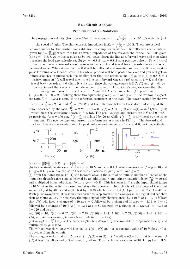
Ver 8284 E1.1 Analysis of Circuits (2016)
E1.1 Circuit Analysis
Problem Sheet 7 - Solutions
The propagation velocity (from page 17-4 of the notes) is u =√
1L0C0
= 2× 10⁸ m/s which is 23 of
the speed of light. The characteristic impedance is Z0 =√
L0
C0= 100 Ω. These are typical
characteristics for the twisted pair cable used in computer networks. The reflection coefficients isgiven by ρ = R−Z0
R+Z0where R is the Thevenin impedance at the relevant end of the line. This gives
(a) ρS = −0.818, ρL = 0 so a pulse at VS will travel down the line as a forward wave and stop whenit reaches the load (no reflections), (b) ρS = −0.818, ρL = 0.818 so a positive pulse at VS will travel
down the line as a forward wave, be reflected at x = L and travel back towards the source as abackward wave. When it reaches x = 0 it will be reflected and inverted and will result in a negativepulse traveling as a forward wave. This whole process will be repeated for ever and you will get aninfinite sequence of pulses each one smaller than than the previous one, (c) ρS = 0, ρL = 0.818 so a
positive pulse at VS will travel down the line as a forward wave, be reflected at x = L and thentravel back towards x = 0 where it will stop. Since the voltage source is DC, f() and g() will be
constants and the waves will be independent of x and t. From Ohm’s law, we know that thevoltage and current in the line are 10 V and 0.2 A so we must have f + g = 10 and
f − g = 0.2× 100 = 20. Solving these two equations gives f = 15 and g = −5. As we would expect,the ratio g
f = −0.333 is equal to the reflection coefficient at the load. The power carried by the two
waves is f2
Z0= 2.25 W and g2
Z0= 0.25 W and the difference between these does indeed equal the
power absorbed by the load: 102
50 = 2 W. At x = 0, v0(t) = f(t) + g(t) and i0(t) = Z−10 (f(t)− g(t))which gives the waveforms shown in Fig. (a). The peak voltage and current are 9 V and 90 mA
respectively. At x = 300 cm, f(t− x
u
)is delayed by 20 ns while g
(t+ x
u
)is advanced by the same
amount. The new voltage and current waveforms are as shown in Fig. (b). The forward andbackward waves now overlap and the peak voltage and current are 12 V and 60 mA respectively.
0 50 100 150 2000
2
4
6
8
10
12
Time (s)
f(t)
, g(t
) an
d v L(t
) (
V)
f(t)
g(t)
vL(t)
Fig. (a) Fig. (b) Fig.
(a) ρL = 100−50100+50 = 0.33, ρ0 = 0−50
0+50 = −1.(b) In the steady state we must have V = 10 V and I = 0.1 A which means that f + g = 10 andf − g = 0.1Z0 = 5. We can solve these two equations to give f = 7.5 and g = 2.5.(c) From the notes (page 17-11) the forward wave is the sum of an infinite number of copies of theinput signal; each extra copy is delayed by an additional round-trip propagation delay (600
15 = 40 ns)and multiplied by an additional factor ρLρ0 = −0.33. This is shown in Fig. ; the input signal jumpsto 10 V when the switch is closed and stays there forever. Onto this is added a copy of the inputsignal delayed by 40 ns and multiplied by −0.33 which means that f(t) jumps to 6.67 at t = 40 ns.With pulse waveforms, it is sometimes easier to keep track of the changes in the signals rather thantheir absolute values. In this case, the input signal only changes once: by +10 V at t = 0. It followsthat f(t) will have a change of +10 at t = 0 followed by a change of 10ρLρ0 = −3.33 at t = 40
followed by a change of 10 (ρLρ0)2
= 1.11 at t = 80 followed by a change of 10 (ρLρ0)3
= −0.37 att = 120 and so on.So, f(0) = 10, f(40) = 6.67, f(80) = 7.78, f(120) = 7.41, f(160) = 7.53, f(200) = 7.49, f(240) =7.5), · · ·. As we can see, f(t)→ 7.5 as predicted in part (a).g(t) = ρLf(t − 2L
u ) is just the same as f(t) but delayed by the round-trip propagation delay andmultiplied by ρl = 0.33.The voltage waveform at x = 0 is equal to f(t) + g(t) and has a constant value of 10 V for t ≥ 0 asis obvious from the circuit.The voltage waveform at x = L is vL(t) = fL(t) + gL(t) = f(t− 20) + g(t+ 20), that is, the sum off(t) delayed by 20 ns and g(t) advanced by 20 ns. This reaches a peak value of 10 (1 + ρL) = 13.3 V.
Solution Sheet 7 Page 1 of 3
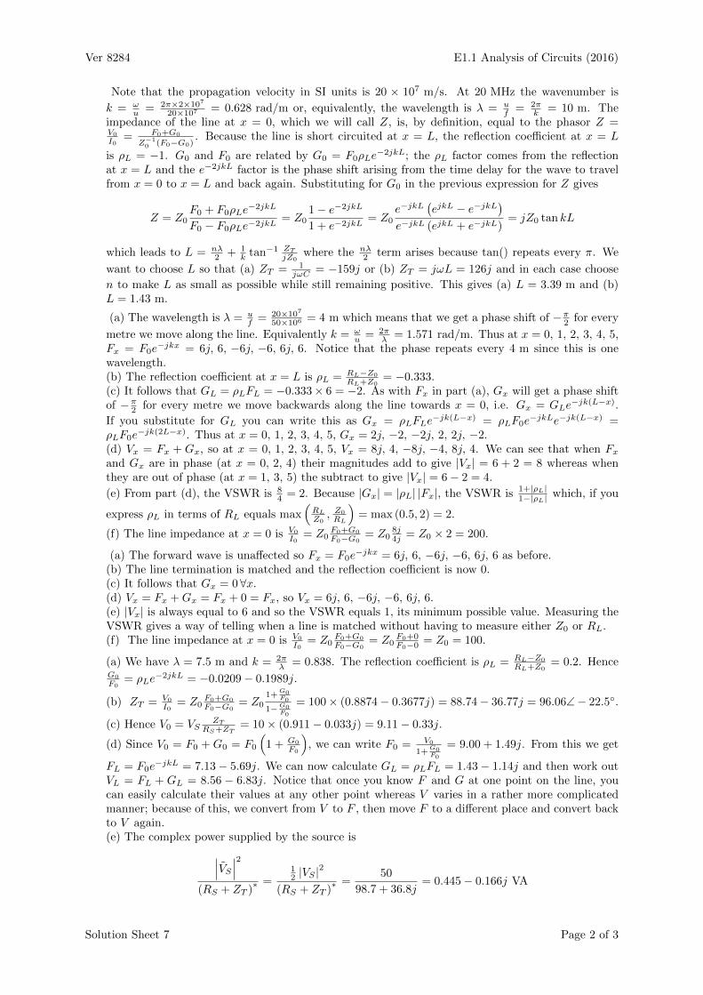
Ver 8284 E1.1 Analysis of Circuits (2016)
Note that the propagation velocity in SI units is 20 × 107 m/s. At 20 MHz the wavenumber is
k = ωu = 2π×2×107
20×107 = 0.628 rad/m or, equivalently, the wavelength is λ = uf = 2π
k = 10 m. Theimpedance of the line at x = 0, which we will call Z, is, by definition, equal to the phasor Z =V0
I0= F0+G0
Z−10 (F0−G0)
. Because the line is short circuited at x = L, the reflection coefficient at x = L
is ρL = −1. G0 and F0 are related by G0 = F0ρLe−2jkL; the ρL factor comes from the reflection
at x = L and the e−2jkL factor is the phase shift arising from the time delay for the wave to travelfrom x = 0 to x = L and back again. Substituting for G0 in the previous expression for Z gives
Z = Z0F0 + F0ρLe
−2jkL
F0 − F0ρLe−2jkL= Z0
1− e−2jkL
1 + e−2jkL= Z0
e−jkL(ejkL − e−jkL
)e−jkL (ejkL + e−jkL)
= jZ0 tan kL
which leads to L = nλ2 + 1
k tan−1 ZT
jZ0where the nλ
2 term arises because tan() repeats every π. We
want to choose L so that (a) ZT = 1jωC = −159j or (b) ZT = jωL = 126j and in each case choose
n to make L as small as possible while still remaining positive. This gives (a) L = 3.39 m and (b)L = 1.43 m.
(a) The wavelength is λ = uf = 20×107
50×106 = 4 m which means that we get a phase shift of −π2 for every
metre we move along the line. Equivalently k = ωu = 2π
λ = 1.571 rad/m. Thus at x = 0, 1, 2, 3, 4, 5,Fx = F0e
−jkx = 6j, 6, −6j, −6, 6j, 6. Notice that the phase repeats every 4 m since this is onewavelength.(b) The reflection coefficient at x = L is ρL = RL−Z0
RL+Z0= −0.333.
(c) It follows that GL = ρLFL = −0.333× 6 = −2. As with Fx in part (a), Gx will get a phase shiftof −π2 for every metre we move backwards along the line towards x = 0, i.e. Gx = GLe
−jk(L−x).
If you substitute for GL you can write this as Gx = ρLFLe−jk(L−x) = ρLF0e
−jkLe−jk(L−x) =ρLF0e
−jk(2L−x). Thus at x = 0, 1, 2, 3, 4, 5, Gx = 2j, −2, −2j, 2, 2j, −2.(d) Vx = Fx + Gx, so at x = 0, 1, 2, 3, 4, 5, Vx = 8j, 4, −8j, −4, 8j, 4. We can see that when Fxand Gx are in phase (at x = 0, 2, 4) their magnitudes add to give |Vx| = 6 + 2 = 8 whereas whenthey are out of phase (at x = 1, 3, 5) the subtract to give |Vx| = 6− 2 = 4.
(e) From part (d), the VSWR is 84 = 2. Because |Gx| = |ρL| |Fx|, the VSWR is 1+|ρL|
1−|ρL| which, if you
express ρL in terms of RL equals max(RL
Z0, Z0
RL
)= max (0.5, 2) = 2.
(f) The line impedance at x = 0 is V0
I0= Z0
F0+G0
F0−G0= Z0
8j4j = Z0 × 2 = 200.
(a) The forward wave is unaffected so Fx = F0e−jkx = 6j, 6, −6j, −6, 6j, 6 as before.
(b) The line termination is matched and the reflection coefficient is now 0.(c) It follows that Gx = 0∀x.(d) Vx = Fx +Gx = Fx + 0 = Fx, so Vx = 6j, 6, −6j, −6, 6j, 6.(e) |Vx| is always equal to 6 and so the VSWR equals 1, its minimum possible value. Measuring theVSWR gives a way of telling when a line is matched without having to measure either Z0 or RL.(f) The line impedance at x = 0 is V0
I0= Z0
F0+G0
F0−G0= Z0
F0+0F0−0 = Z0 = 100.
(a) We have λ = 7.5 m and k = 2πλ = 0.838. The reflection coefficient is ρL = RL−Z0
RL+Z0= 0.2. Hence
G0
F0= ρLe
−2jkL = −0.0209− 0.1989j.
(b) ZT = V0
I0= Z0
F0+G0
F0−G0= Z0
1+G0F0
1−G0F0
= 100× (0.8874− 0.3677j) = 88.74− 36.77j = 96.06∠− 22.5.
(c) Hence V0 = VSZT
RS+ZT= 10× (0.911− 0.033j) = 9.11− 0.33j.
(d) Since V0 = F0 + G0 = F0
(1 + G0
F0
), we can write F0 = V0
1+G0F0
= 9.00 + 1.49j. From this we get
FL = F0e−jkL = 7.13− 5.69j. We can now calculate GL = ρLFL = 1.43− 1.14j and then work out
VL = FL + GL = 8.56 − 6.83j. Notice that once you know F and G at one point on the line, youcan easily calculate their values at any other point whereas V varies in a rather more complicatedmanner; because of this, we convert from V to F , then move F to a different place and convert backto V again.(e) The complex power supplied by the source is∣∣∣VS∣∣∣2
(RS + ZT )∗ =
12 |VS |
2
(RS + ZT )∗ =
50
98.7 + 36.8j= 0.445− 0.166j VA
Solution Sheet 7 Page 2 of 3

Ver 8284 E1.1 Analysis of Circuits (2016)
. You might expect this to be purely real because the circuit appears to contain only resistors;however, there are implicit capacitors and inductors in the transmission line.
Solution Sheet 7 Page 3 of 3