eece 481 mos basics - courses.ece.ubc.ca
TRANSCRIPT

1
EECE 481
MOS Basics Lecture 2
EECE 481 Lecture 2
Reza Molavi
Dept. of ECE
University of British Columbia
Slides Courtesy : Dr. Res Saleh (UBC), Dr. D. Sengupta (AMD), Dr. B. Razavi (UCLA)

2 EECE 481 Lecture 2
PN Junction and Diodes
PN Junction
- The difference in the concentration of carriers in p, and n-type semi-conductors (i.e. gradient)
causes diffusion of electrons from n to p and holes from p to n leaving immobile ions behind
- The region at junction where majority carriers are removed due to this diffusion, is called the
depletion or space-charge region
p-type semi-conductor heavily
doped with acceptor atoms,
e.g. boron
n-type semi-conductor is
heavily doped with donor
atoms, e.g. arsenic and
phosphorus

3 EECE 481 Lecture 2
PN Junction Basics
- The charges in both regions create an electric field across the boundary of junction to
counteract the diffusion of majority carriers
-This electric field creates a potential across the junction called contact or barrier potential

4 EECE 481 Lecture 2
PN Junction - Equilibrium
Majority carriers are abundant at equilibrium (on either side) but can not diffuse to the other
side due to the existence of barrier potential

5 EECE 481 Lecture 2
PN Junction – Forward Bias

6 EECE 481 Lecture 2
MOS Transistor Basics
The source and drain regions (n+) and substrate (p) in NMOS transistor create
two back-to-back diodes at equilibrium (therefore, requires external stimulus for any conduction)

7 EECE 481 Lecture 2
Definition of Threshold Voltage
- We need to apply an external voltage to turn the p-type substrate into an n-type substrate to
create a channel for conduction
- As we apply a positive VGS the substrate is first depleted under the gate area (immobile ions)
- Further increase of VGS creates a conducting layer of minority carriers under the gate
- The VGS voltage required to make the surface of the substrate “as much n-type as the rest of
substrate is p” is called Threshold Voltage

8 EECE 481 Lecture 2
Definition of Threshold Voltage
The onset of inversion in NMOS transistor (creation of channel under the gate in (d)
Small VGS, no channel yet!

9 EECE 481 Lecture 2
Effect of Body bias on Threshold Voltage
- Application of negative voltage to bulk attracts holes and leaves behind “negatively charged ions”
- As a result, there should be more positive charge on gate plate to mirror the negative ions in the
substrate and more positive voltage is required to create the channel, i.e. VTH increases
where

10 EECE 481 Lecture 2
MOS Current Calculation
Charge per unit area
VDS > 0 carriers start flowing
From source into the drain
VGS > Vth channel created,
no current yet!

11 EECE 481 Lecture 2
MOS Current Calculation
Charge density along direction of current
Velocity of carriers is a function of
the horizontal electric field
Total charge in the grey box (amount of charge hat
passes through the channel in 1 second)

12 EECE 481 Lecture 2
MOS Current Calculation
This equation predicts roll-off after reaching a peak due to the existence of non-physical
positive carriers. Therefore, the equation must be adjusted after VDS reaches VGS-VT
(Board Notes)
13 EECE 481 Lecture 2
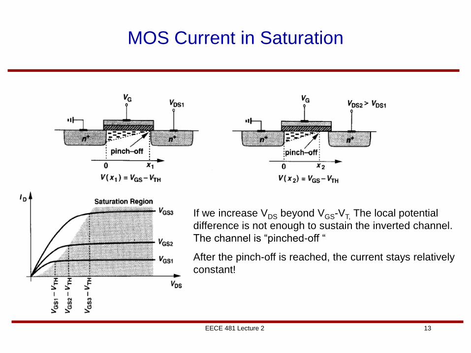
MOS Current in Saturation
If we increase VDS beyond VGS-VT, The local potential
difference is not enough to sustain the inverted channel.
The channel is “pinched-off “
After the pinch-off is reached, the current stays relatively
constant!

14 EECE 481 Lecture 2
Channel-length Modulation
(IDS dependence on VDS)
Large drain-source voltage makes the channel
Effectively smaller, i.e. larger drain current
(Board Notes)

15 EECE 481 Lecture 2
Large E Fields in Short Channel Devices
Horizontal Electric field (between the source and drain) = VDS (=Vdd) / L
Vertical Electric field (between the gate and channel) = VGS (=Vdd) / tox
Large electrical field causes an early velocity saturation for carriers in short channel devices

16 EECE 481 Lecture 2
Velocity Saturation
- Beyond a certain field limit velocity does not increase!
- NMOS saturates faster than PMOS (due to their
larger mobility)

17 EECE 481 Lecture 2
Short-Channel MOS Current
Similar to long channel device except for an extra term in denominator
General current of short channel MOS

18 EECE 481 Lecture 2
Cont’d
Current of short channel MOS in saturation
Equating this current and that of previous slide gives the required VDS for saturation
Always smaller than VGS-VT
indicates early saturation
(Board Notes)

19 EECE 481 Lecture 2
Example From Hodges and Saleh Textbook
- Note how fast NMOS saturates (at VDS of 0.6 rather than 1.3 (1.8-0.5)
- Note the difference between NMOS and PMOS

20 EECE 481 Lecture 2
Summary
• Semi-conductor devices typically possess an inherent barrier of
current and a control knob (voltage) to remove the barrier.
• Threshold Voltage is the required gate-source voltage to invert
the substrate to the opposite type, i.e. p to n for NMOS and n
and to p for PMOS to create a conductive channel.
• As VDS increases the MOS devices are first in linear(triode
region) and then enter saturation regime (relatively constant
current, channel length modulation still applies).
• Large Electrical fields (both vertical and horizontal) causes early
saturation of DSM devices.
• For short-channel devices the IDS-VGS relationship is more
linear rather than quadratic.