efficient architecture for flexible prescaler using...
TRANSCRIPT

International Journal of Science, Engineering and Technology Research (IJSETR), Volume 3, Issue 3, March 2014
571
ISSN: 2278 – 7798
All Rights Reserved © 2014 IJSETR
Abstract— This paper, An Efficient Architecture for Flexible
Prescaler Using Multimodulo Prescaler is an architecture which is designed from the proposed dynamic logic multiband flexible divider. The multiband divider consist of different Multimodulo Prescaler by using different N/N+1 dual modulo Prescaler we get different Multimodulo Prescaler. In this paper, it shows the power reduction by using four Prescaler in one block is less than that of two Prescaler in one block.
Keywords—prescaler,dualmoduloPrescaler,dynamic
logic,DFF
I. INTRODUCTION
Division operation is very important in the computer
system. For division algorithm now a day‗s people use a
hardware module divider. So many techniques are there to
implement the divider. In synchronous technique it always
need clock signal to trigger the system. If we use that
technique it may cause some problems, such as clock skew,
dynamic power consumption... etc. If we compared with
synchronous systems, asynchronous circuits do not need
system clock signals and thus the asynchronous system does
not have the shortcomings mentioned above.
Wireless communication has received increasing interest
for military and commercial applications. The Wireless LAN
(WLAN) it operates in different frequency band, in market a
leading WLAN solutions must offer multi-mode
interoperability with transparent worldwide usage. The
design for frequency synthesizers is for fast switching and for
high operating frequencies. The synthesizer can be an
integer-N type with programmable Integer frequency
dividers or Fractional-N type synthesizer. By using dual
modulo Prescaler that is N or N+1 we can do frequency
division.
Frequency dividers (FDs) also called Prescaler which are
used in many communications applications such as
frequency synthesizers, timing-recovery circuits and clock
generation circuits. The Prescaler is loaded at the feedback
path of the synthesizer, takes signal and generate a periodic
output signal and frequency is fraction of the input
frequency. Prescaler is one of the most critical blocks in the
frequency synthesizer since it operates at the highest
Manuscript received Feb , 2014.
G SWETHA, VLSI DESIGN, SRM UNIVERSITY Chennai, India,
9962214181
S Yuvaraj, ELACTRONICS AND COMMUNICATION ENGINEERING ,
SRM University, Chennai, India, Phone/ Mobile No.9715340404
frequency and consumes large power. So, there must be
power reduction in the first stage of
Prescaler so it is an important one to realize the low power.
Fig. 1 a new architecture of dynamic logic multiband flexible divider
I. DESIGN PARAMETERS
In electronics, digital circuits and digital electronics, the
propagation delay, or gate delay, is the length of time which
starts when the input to a logic gate becomes stable and valid,
at that time the output of that logic gate is stable and valid.
When input changes it takes some time to reach 0.1% to
0.9% of its final output level. If we reduce the gate delay in
the circuit, then the process will be faster and has a good
performance.
Propagation delay increased due to temperature, supply
voltage and output load capacitance. The output of a logic
gate is connected to many other gates (high fan-out) the
propagation delay increases substantially. Wires have an
approximate propagation delay of 1 ns for every 6 inches (15
cm) of length. Logic gates can have delays ranges from more
than 10 ns. The operating frequency is decided by the
propagation delay and it is calculated as
(1)
In equation (1) tpLH is a low to high transition and tpHL
is a high to low transition of the gates. The total power
consumption of the CMOS digital circuits is determined by
the switching and short circuit power. The switching power
Efficient Architecture for Flexible Prescaler
Using
Multimodulo Prescaler
G SWETHA, S YUVARAJ
International Journal of Science, Engineering and Technology Research (IJSETR), Volume 3, Issue 3, March 2014
572
All Rights Reserved © 2014 IJSETR
is linearly proportional to the operating frequency and is
given by the sum of switching power at each output node as in
(2)
Where n is the number of switching nodes, fclk is the clock
frequency, CLi is the load capacitance at the output node of
the i th stage, and Vdd is the supply voltage. Normally, the
short-circuit power occurs in dynamic circuits when there
exists direct paths from the supply to ground which is given
by
Psc = Isc*Vdd (3)
Where Isc is the short-circuit current. From this it shows
that the short-circuit power is much higher in E-TSPC logic
circuits than in TSPC logic circuits. Where, TSPC logic
circuits exhibit higher switching power compared to that of
E-TSPC logic circuits due to high load capacitance. For the
E-TSPC logic circuit, the short-circuit power is the major
problem. The ETSPC circuit has the merit of higher
operating frequency, but it consumes more power than the
TSPC circuit does for a given transistor size.
II. Dual modulo Prescaler
a) 2/3 Prescaler
Fig. 2 Single-Phase Clock 2/3Prescaler
In conventional 2/3 Prescaler uses two DFF‘s.DFF1 is
loaded by OR gate and DFF2 is loaded by DFF1, an AND
gate in the output stage which makes a larger load. A low
power and improved speed 2/3 Prescaler implemented in the
TSPC logic format. Fig. 2 shows the Prescaler which uses
two embedded NOR gates instead of an OR, AND gate for the
conventional 2/3 TSPC Prescaler. This arrangement reduces
the switching nodes 12 to 7 and consumes less power
compared to the conventional 2/3 Prescaler.
The control signal MC selects the divide by 2 or 3 mode.
When MC is logic 1 DFF1 will disconnect from the power
supply and DFF2 alone work to form the divide-by-2
operation. Therefore the short circuit power and switching
power DFF1 is removed. When MC Low both flip-flops
combine give the divide-by-3 operation.
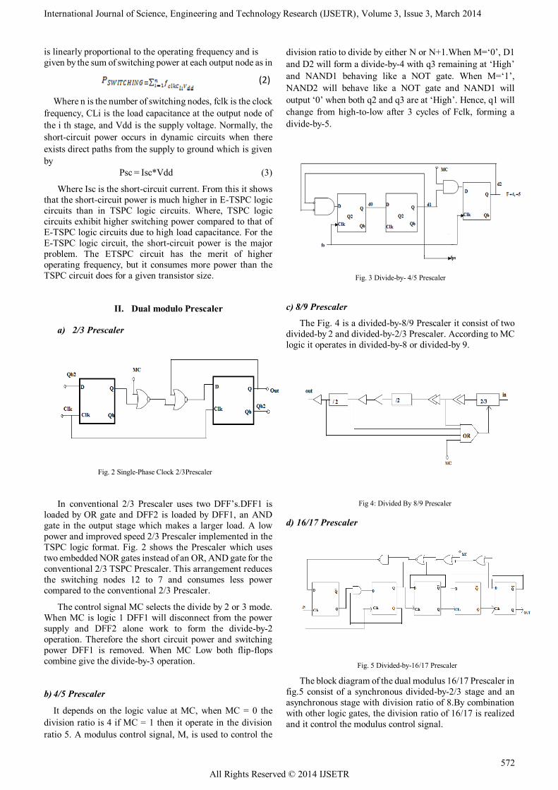
b) 4/5 Prescaler
It depends on the logic value at MC, when MC = 0 the
division ratio is 4 if MC = 1 then it operate in the division
ratio 5. A modulus control signal, M, is used to control the
division ratio to divide by either N or N+1.When M=‗0‘, D1
and D2 will form a divide-by-4 with q3 remaining at ‗High‘
and NAND1 behaving like a NOT gate. When M=‗1‘,
NAND2 will behave like a NOT gate and NAND1 will
output ‗0‘ when both q2 and q3 are at ‗High‘. Hence, q1 will
change from high-to-low after 3 cycles of Fclk, forming a
divide-by-5.
Fig. 3 Divide-by- 4/5 Prescaler
c) 8/9 Prescaler
The Fig. 4 is a divided-by-8/9 Prescaler it consist of two
divided-by 2 and divided-by-2/3 Prescaler. According to MC
logic it operates in divided-by-8 or divided-by 9.
Fig 4: Divided By 8/9 Prescaler
d) 16/17 Prescaler
Fig. 5 Divided-by-16/17 Prescaler
The block diagram of the dual modulus 16/17 Prescaler in
fig.5 consist of a synchronous divided-by-2/3 stage and an
asynchronous stage with division ratio of 8.By combination
with other logic gates, the division ratio of 16/17 is realized
and it control the modulus control signal.

International Journal of Science, Engineering and Technology Research (IJSETR), Volume 3, Issue 3, March 2014
573
ISSN: 2278 – 7798
All Rights Reserved © 2014 IJSETR
III. MULTIMODULOS 32/33/47/48 PRESCALER
The proposed wideband Multimodulo Prescaler
which can divide the input frequency by 32, 33, 47, and 48 is
shown in Fig. 3. It is similar to the 32/33 Prescaler used in,
but with an additional inverter and a multiplexer without any
extra flip-flop it can also perform 47 and 48 and also it saves
the power, reduces the complexity. The Multimodulo
Prescaler consists of the wideband 2/3 (N1/(N+1))Prescaler ,
four asynchronous TSPC divide-by-2 circuits ((AD)=16) and
combinational logic circuits to achieve multiple division
ratios. Besides the usual MOD signal for controlling N /
(N+1) divisions, the additional control signal Sel is used to
switch the Prescaler between 32/33 and 47/48 modes.
Fig. 6 Multimodulo Prescaler
Case 1: S =’0’
When Sel=0, the output from the NAND2 gate is directly
transferred to the input of 2/3 Prescaler and the Multimodulo
Prescaler operates as the normal 32/33 Prescaler, where the
division ratio is controlled by the logic signal MOD. If
MC=1, the 2/3 Prescaler operates in the divide-by-2 mode
and when MC, the 2/3 Prescaler operates in the divide-by-3
mode. If MOD =1, the NAND2 gate output switches to
logic-1‖ (MC=1) and the wideband Prescaler operates in the
divide- by-2 mode for entire operation.
The division ratio N performed by the Multimodulo
Prescaler is
N = (AD*N)+(0*(N+1)) = 32
(4)
Where N=2 and AD=16 is fixed for the entire design. If
MOD=0 , for 30 input clock cycles MC remains at logic ―1,
where wideband Prescaler operates in divide-by-2 mode and,
for three input clock cycles, MC remains at logic ―0‖ where
the wideband Prescaler operates in the divide-by-3 mode.
The division ratio N+1 performed by the Multimodulo
Prescaler is
N + 1 = ((AD – 1)*N)+(1*(N+1)) =33
(5)
Case 2: S = 1
When Sel = 1, the inverted output of the NAND2 gate is
directly transferred to the input of 2/3 Prescaler and the
Multimodulo Prescaler operates as a 47/48 Prescaler, where
the division ratio is controlled by the logic signal MOD. If
MC= 1, the 2/3 Prescaler operates in divide-by-3 mode and
when MC=0, the 2/3 Prescaler operates in divide-by-2 mode
which is quite opposite to the operation performed when
Sel=0.
If MOD = 1, the division ratio N+1 performed by the
multi modulus Prescaler is same as except that the wideband
Prescaler operates in the divide-by-3 mode for the entire
operation given by
N + 1 = ((AD *(N+1))+(0*N)) = 48
(6)
If MOD = 1, the division ratio N performed by the Multi
Modulus Prescaler is
N = ((AD - 1) * (N+1)) + (1*N) = 47 (7)
For divided-by-2/3 Prescaler we get 32/33/47/48
Multimodulo Prescaler. In that way in the place proposed 2/3
Prescaler if we keep 4/5 Prescaler we get 64/65/79/80
Multimodulo Prescaler. And for 8/9 Prescaler we get
128/129/143/144.In the same way for 16/17 Prescaler we get
256/257/271/272 Multimodulo Prescaler.
IV. MULTIBAND FLEXIBLE DIVIDER
a) Program Counter
The program counter is responsible for counting P pulses
of Slow CLK before outputting a pulse to the
phase/frequency detector and resetting itself and the swallow
counter. The implementation used in this project, using a
7-bit ripple counter, a 7-bit comparator, and a zero-detector
is shown in Figure. The ripple counter is clocked by Slow
CLK, and increments its count by one each clock cycle. At
each stage, the 7-bit comparator compares each count bit to
the corresponding bit in the control signal, and outputs a 0
for each equal bit. When the zero-detector detects
equivalence in all of the 7 bits, indicating that the desired
count has been reached, Fout is driven high. On the next
clock cycle, the program counter is reset to zero and the count
is restarted. In addition, the output pulse on Fout is used to
reset the count of the swallow counter, indicating the end of
one complete cycle of the frequency divider.
The ripple counter is implemented using 7 cascaded
D-type flip-flops, each arranged in a toggle configuration.
The output of each flip-flop is used to clock the next flip-flop.
Since the output of each flip-flop inverts on every clock cycle,
each flip-flop essentially divides its clock by two, causing the
next stage of the ripple counter to be clocked at half the rate
of the previous flip flop. Each flip-flop was designed to
respond to the falling edge of its clock, when the output of the
previous stage changes from a 1 to a 0. In this way, an
incrementing binary count is achieved with the outputs of
each flip-flop forming the bits of the count. Since the
program counter contains 7-bits, any count between 0 and
127 can be set by the control signal. It is important to realize
however that in order to achieve a division ratio as specified
in the equation DIV=NP+S, the control signal must be set to
P-1, since the zero-state is included in the count.

International Journal of Science, Engineering and Technology Research (IJSETR), Volume 3, Issue 3, March 2014
574
All Rights Reserved © 2014 IJSETR
Fig. 7 Block Diagram Of A 7-bit Program Counter
Program Counter Implementation
It is possible to see the three major components of the
program counter implemented using MCML logic gates. At
the input of the counter, an array of 7 flip-flops is used as the
ripple counter. The outputs of the ripple counter, taken from
the outputs of each of the flip-flops, are fed into an array of 7
XNOR gates. The XNOR gates compare each bit with the
corresponding bit in the control signal, outputting a logical
‗1‗ when the bits are equal. Although this logic is inverted
compared to the description of the comparator in the previous
section, the zero-detector is implemented as a one-detector
using a tree of cascaded AND gates. In this way, the overall
logic of the circuit is unchanged, and the output pulse can be
generated without any additional logic. Another difference
seen in Figure is a separate output, Swallow RST, and some
simple circuitry used to generate it.
Swallow RST is used internally to reset the flip-flops of
the program counter, and externally to reset the flip-flops of
the swallow counter. Since the fan-out of the reset signal is
high (7 flip-flops in the PC, and 6 in the SC), the reset signal
is broken into two paths and driven using separate MCML
buffers. In early simulations, these buffers were absent and
the reset signal could not provide enough current to drive the
input capacitance associated with the flip-flops. Swallow
RST was generated using an approach that guarantees
predictable timing of the reset signal. Fout is ―tapped‖ and
fed to the input of a flip-flop clocked by Fin. On the clock
cycle immediately following Fout going high, the pulse is
sampled by the flip-flop, generating Swallow RST and
resetting both the program counter and the swallow counter.
To ensure that the reset signal is removed before the next
clock cycle, the reset signal is fed back to its generating
flip-flop through a delay chain comprised of three buffers.
a) Swallow Counter
The swallow counter, as indicated in Figure, is used to
count S pulses of Slow CLK before asserting the modulus
control signal and changing the modulus of the DMP to N. A
block diagram of the swallow counter is provided in Figure.
By looking at Figure, the similarities between the swallow
counter and the program counter are apparent. Once again,
the count (6-bits in this case) is maintained using a ripple
counter comprised of cascaded flip-flops clocked with Slow
CLK. In addition, a comparator compares each count bit with
its corresponding bit in the control signal, and a
zero-detector asserts modulus control when all bits are equal.
However, the swallow counter does not reset when the count
is reached, but masks the input clock using an AND gate
connected to the inverse of modulus control. As a result, the
ripple counter stops counting when the count is reached, and
the state of the circuit is maintained until a reset signal
(Swallow RST) is received from the program
Fig.8 Block Diagram Of 6-bit Swallow Counter
S-Counter Implementation
The 6-bit ripple counter implemented as an array of
flip-flops, and clocked with the gated clock provided by the
AND of Slow CLK and modulus control. In addition, the
comparator is implemented as an array of MCML XNOR
gates, while the zero-detector is actually implemented as a
one-detector using a tree of cascaded AND gates. Unlike the
program counter however, no additional circuitry is
necessary to generate the reset as the reset is received from
the program counter by means of the Swallow RST signal.By
implementing individual block and placing the entire blocks
a new block diagram of dynamic logic multiband flexible
divider is formed.
I. OPERATION
Always clock is high and the 7-bit control signal of
Program counter is 1100000 and 6-bit control signal of
Swallow counter is 011000.The output is show below in
tabular form with different Prescaler and Mux inputs the
output will be varied in to 2/3, 4/5, 8/9, 16/17 Prescaler and
executes Multimodulo Prescaler in the graph which is shown
below tabular form and it is done with HDL program.

International Journal of Science, Engineering and Technology Research (IJSETR), Volume 3, Issue 3, March 2014
575
ISSN: 2278 – 7798
All Rights Reserved © 2014 IJSETR
TABLE I
Prescaler input Mux input Output
Multimodulo
Prescaler
10 00 2/3 32/33/47/48
11 01 4/5 64/65/79/80
00 10 8/9 126/127/143/144
01 11 16/17 256/257/271/272
When Prescaler input is 10 and Mux input is 00 the output is 2/3 Prescaler that is 32/33/47/48 Multimodulo Prescaler
When Prescaler input is 11 and Mux input is 01 the output is 4/5 Prescaler that is 64/65/79/80 Multimodulo Prescaler

International Journal of Science, Engineering and Technology Research (IJSETR), Volume 3, Issue 3, March 2014
576
All Rights Reserved © 2014 IJSETR
When Prescaler input is 00 and Mux input is 10 the output is 8/9 Prescaler that is 128/128/143/144 Multimodulo Prescaler.
When Prescaler input 01 and Mux input 11 the output is 16/17 Prescaler that is 256/257/271/272 Multimodulo Prescaler.

International Journal of Science, Engineering and Technology Research (IJSETR), Volume 3, Issue 3, March 2014
577
ISSN: 2278 – 7798
All Rights Reserved © 2014 IJSETR
POWER REPORT
TABLE II
SIMULATION RESULTS
The power report which is mentioned in TABLE II taken
from the Xilinx tool and the output is shown below.
Frequency Divider 2/3 and 4/5
Frequency Divider 2/3, 4/5, 8/9, 16/17
CONCLUSION
In the proposed system they designed dynamic logic
flexible divider. In this paper, a new architecture is designed
with four Prescaler that is 2/3, 4/7, 8/9, 16/17 and combining
all the four Prescaler, and it takes less power when compared
to two Prescaler in one block that is 2/3 and 4/5 Prescaler.
And it is synthesized from the Model Sim and power report is
taken from the X power. The frequency division is applicable
for many applications and in real time also.
REFERENCES
[1] V. K. Manthena “A Low-Power Single-Phase
Clock Multiband Flexible Divider,‖ IEEE
transactions on very large scale integration (VLSI)
systems, vol.20, n0.20, February 2012.(reference)
[2] V. K. Manthena ―A 1.8-V 6.5-GHz low power wide
and single-phase clock CMOS 2/3 Prescaler,‖ in
IEEE 53rd Midwest Symp. Circuits Syst., Aug.
2010, pp. 149–152.
[3] V. K. Manthena “A low power fully programmable
1 MHz resolution 2.4 GHz CMOS PLL frequency
synthesizer,” in Proc. IEEE Biomed. Circuits Syst.
Conf., Nov. 2007, pp. 187–190.
[4] Li Wang ―A 16/17 Dual-Modulus Prescaler in SiGe
HBT Technology‖.
[5] Ali Rahnamaei “Design and Optimization of
÷8/9 Divider in PLL Frequency Synthesizer with
Dynamic Logic (E_TSPC)‖. Proceedings of the 6th
WSEAS Int. Conf. on Electronics, Hardware,
Wireless and Optical Communications, Corfu
Island, Greece, February 16-19, 2007.
About Author
G Swetha received B.Tech degree in Electronics &
Communication Engineering from Nimra College
of Engineering & Technology, Ibrahimpatnam,
Vijayawada, Andhra Pradesh, India. Currently
doing M.Tech in specialization of VLSI DESIGN in
SRM UNIVERSITY, Chennai.
.
S Yuvaraj received B.E degree in Electronics &
Communication Engineering from KSR College of
Engineering, Tamil Nadu, India and M.Tech in VLSI
DESIGN from the SRM UNIVERSITY, Chennai, India.
Currently he is working as Associate Professor O.G at SRM
UNIVERSITY, Chennai, Tamil Nadu.
Prescaler Multimodulo
Prescaler Power(Mw)
Combine of
2/3 and 4/5
Prescaler
32/33/47/48
and 64/65/79/80 1746 mw
Combined
2/3,4/5,8/9,16/17
Prescaler
32/33/47/48,
64/65/79/80,
128/129/143/144
256/257/272/271
1593 mw