electromagnetic -...
TRANSCRIPT


Electromagnetic Advanced Design System 2012.08

1
Copyright Notice
© Agilent Technologies, Inc. 1983-2012 5301 Stevens Creek Blvd., Santa Clara, CA 95052 USA No part of this documentation may be reproduced in any form or by any means (including electronic storage and retrieval or translation into a foreign language) without prior agreement and written consent from Agilent Technologies, Inc. as governed by United States and international copyright laws.
Acknowledgments Mentor Graphics is a trademark of Mentor Graphics Corporation in the U.S. and other countries. Mentor products and processes are registered trademarks of Mentor Graphics Corporation. * Calibre is a trademark of Mentor Graphics Corporation in the US and other countries. "Microsoft®, Windows®, MS Windows®, Windows NT®, Windows 2000® and Windows Internet Explorer® are U.S. registered trademarks of Microsoft Corporation. Pentium® is a U.S. registered trademark of Intel Corporation. PostScript® and Acrobat® are trademarks of Adobe Systems Incorporated. UNIX® is a registered trademark of the Open Group. Oracle and Java and registered trademarks of Oracle and/or its affiliates. Other names may be trademarks of their respective owners. SystemC® is a registered trademark of Open SystemC Initiative, Inc. in the United States and other countries and is used with permission. MATLAB® is a U.S. registered trademark of The Math Works, Inc.. HiSIM2 source code, and all copyrights, trade secrets or other intellectual property rights in and to the source code in its entirety, is owned by Hiroshima University and STARC. FLEXlm and FLEXnet are registered trademarks of Flexera Software LLC Terms of Use for Flexera Software information can be found at http://www.flexerasoftware.com/company/about/terms.htm . Layout Boolean Engine by Klaas Holwerda, v1.7 http://www.xs4all.nl/~kholwerd/bool.html . FreeType Project, Copyright (c) 1996-1999 by David Turner, Robert Wilhelm, and Werner Lemberg. QuestAgent search engine (c) 2000-2002, JObjects. Motif is a trademark of the Open Software Foundation. Netscape is a trademark of Netscape Communications Corporation. Netscape Portable Runtime (NSPR), Copyright (c) 1998-2003 The Mozilla Organization. A copy of the Mozilla Public License is at http://www.mozilla.org/MPL/ . FFTW, The Fastest Fourier Transform in the West, Copyright (c) 1997-1999 Massachusetts Institute of Technology. All rights reserved. Gradient, HeatWave and FireBolt are trademarks of Gradient Design Automation Inc.
The following third-party libraries are used by the NlogN Momentum solver:
"This program includes Metis 4.0, Copyright © 1998, Regents of the University of Minnesota", http://www.cs.umn.edu/~metis , METIS was written by George Karypis ([email protected]).
Intel@ Math Kernel Library, http://www.intel.com/software/products/mkl
HSPICE is a registered trademark of Synopsys, Inc. in the United States and/or other countries.
DWG and DXF are registered trademarks of Autodesk, Inc. in the United States and/or other countries.
MATLAB is a registered trademark of The MathWorks, Inc. in the United States and/or other countries.
SuperLU_MT version 2.0 - Copyright © 2003, The Regents of the University of California, through Lawrence Berkeley National Laboratory (subject to receipt of any required approvals from U.S. Dept. of Energy). All rights reserved. SuperLU Disclaimer: THIS SOFTWARE IS PROVIDED BY THE COPYRIGHT HOLDERS AND CONTRIBUTORS "AS IS" AND ANY EXPRESS OR IMPLIED WARRANTIES, INCLUDING, BUT NOT LIMITED TO, THE IMPLIED WARRANTIES OF MERCHANTABILITY AND FITNESS FOR A PARTICULAR PURPOSE ARE DISCLAIMED. IN NO EVENT SHALL THE COPYRIGHT OWNER OR CONTRIBUTORS BE LIABLE FOR ANY DIRECT, INDIRECT, INCIDENTAL, SPECIAL, EXEMPLARY, OR CONSEQUENTIAL DAMAGES (INCLUDING, BUT NOT LIMITED TO, PROCUREMENT OF SUBSTITUTE GOODS OR SERVICES;

Electromagnetic
2
LOSS OF USE, DATA, OR PROFITS; OR BUSINESS INTERRUPTION) HOWEVER CAUSED AND ON ANY THEORY OF LIABILITY, WHETHER IN CONTRACT, STRICT LIABILITY, OR TORT (INCLUDING NEGLIGENCE OR OTHERWISE) ARISING IN ANY WAY OUT OF THE USE OF THIS SOFTWARE, EVEN IF ADVISED OF THE POSSIBILITY OF SUCH DAMAGE.
7-zip - 7-Zip Copyright: Copyright (C) 1999-2009 Igor Pavlov. Licenses for files are: 7z.dll: GNU LGPL + unRAR restriction, All other files: GNU LGPL. 7-zip License: This library is free software; you can redistribute it and/or modify it under the terms of the GNU Lesser General Public License as published by the Free Software Foundation; either version 2.1 of the License, or (at your option) any later version. This library is distributed in the hope that it will be useful,but WITHOUT ANY WARRANTY; without even the implied warranty of MERCHANTABILITY or FITNESS FOR A PARTICULAR PURPOSE. See the GNU Lesser General Public License for more details. You should have received a copy of the GNU Lesser General Public License along with this library; if not, write to the Free Software Foundation, Inc., 59 Temple Place, Suite 330, Boston, MA 02111-1307 USA. unRAR copyright: The decompression engine for RAR archives was developed using source code of unRAR program.All copyrights to original unRAR code are owned by Alexander Roshal. unRAR License: The unRAR sources cannot be used to re-create the RAR compression algorithm, which is proprietary. Distribution of modified unRAR sources in separate form or as a part of other software is permitted, provided that it is clearly stated in the documentation and source comments that the code may not be used to develop a RAR (WinRAR) compatible archiver. 7-zip Availability: http://www.7-zip.org/
AMD Version 2.2 - AMD Notice: The AMD code was modified. Used by permission. AMD copyright: AMD Version 2.2, Copyright © 2007 by Timothy A. Davis, Patrick R. Amestoy, and Iain S. Duff. All Rights Reserved. AMD License: Your use or distribution of AMD or any modified version of AMD implies that you agree to this License. This library is free software; you can redistribute it and/or modify it under the terms of the GNU Lesser General Public License as published by the Free Software Foundation; either version 2.1 of the License, or (at your option) any later version. This library is distributed in the hope that it will be useful, but WITHOUT ANY WARRANTY; without even the implied warranty of MERCHANTABILITY or FITNESS FOR A PARTICULAR PURPOSE. See the GNU Lesser General Public License for more details. You should have received a copy of the GNU Lesser General Public License along with this library; if not, write to the Free Software Foundation, Inc., 51 Franklin St, Fifth Floor, Boston, MA 02110-1301 USA Permission is hereby granted to use or copy this program under the terms of the GNU LGPL, provided that the Copyright, this License, and the Availability of the original version is retained on all copies.User documentation of any code that uses this code or any modified version of this code must cite the Copyright, this License, the Availability note, and "Used by permission." Permission to modify the code and to distribute modified code is granted, provided the Copyright, this License, and the Availability note are retained, and a notice that the code was modified is included. AMD Availability: http://www.cise.ufl.edu/research/sparse/amd
UMFPACK 5.0.2 - UMFPACK Notice: The UMFPACK code was modified. Used by permission. UMFPACK Copyright: UMFPACK Copyright © 1995-2006 by Timothy A. Davis. All Rights Reserved. UMFPACK License: Your use or distribution of UMFPACK or any modified version of UMFPACK implies that you agree to this License. This library is free software; you can redistribute it and/or modify it under the terms of the GNU Lesser General Public License as published by the Free Software Foundation; either version 2.1 of the License, or (at your option) any later version. This library is distributed in the hope that it will be useful, but WITHOUT ANY WARRANTY; without even the implied warranty of MERCHANTABILITY or FITNESS FOR A PARTICULAR PURPOSE. See the GNU Lesser General Public License for more details. You should have received a copy of the GNU Lesser General Public License

3
along with this library; if not, write to the Free Software Foundation, Inc., 51 Franklin St, Fifth Floor, Boston, MA 02110-1301 USA Permission is hereby granted to use or copy this program under the terms of the GNU LGPL, provided that the Copyright, this License, and the Availability of the original version is retained on all copies. User documentation of any code that uses this code or any modified version of this code must cite the Copyright, this License, the Availability note, and "Used by permission." Permission to modify the code and to distribute modified code is granted, provided the Copyright, this License, and the Availability note are retained, and a notice that the code was modified is included. UMFPACK Availability: http://www.cise.ufl.edu/research/sparse/umfpack UMFPACK (including versions 2.2.1 and earlier, in FORTRAN) is available at http://www.cise.ufl.edu/research/sparse . MA38 is available in the Harwell Subroutine Library. This version of UMFPACK includes a modified form of COLAMD Version 2.0, originally released on Jan. 31, 2000, also available at http://www.cise.ufl.edu/research/sparse
. COLAMD V2.0 is also incorporated as a built-in function in MATLAB version 6.1, by The MathWorks, Inc. http://www.mathworks.com . COLAMD V1.0 appears as a column-preordering in SuperLU (SuperLU is available at http://www.netlib.org ). UMFPACK v4.0 is a built-in routine in MATLAB 6.5. UMFPACK v4.3 is a built-in routine in MATLAB 7.1.
Qt Version 4.7.4 - Qt Notice: The Qt code was modified. Used by permission. Qt copyright: Qt Version 4.7.4, Copyright (c) 2010 by Nokia Corporation. All Rights Reserved. Qt License: Your use or distribution of Qt or any modified version of Qt implies that you agree to this License. This library is free software; you can redistribute it and/or modify it under the terms of the GNU Lesser General Public License as published by the Free Software Foundation; either version 2.1 of the License, or (at your option) any later version. This library is distributed in the hope that it will be useful, but WITHOUT ANY WARRANTY; without even the implied warranty of MERCHANTABILITY or FITNESS FOR A PARTICULAR PURPOSE. See the GNU Lesser General Public License for more details. You should have received a copy of the GNU Lesser General Public License along with this library; if not, write to the Free Software Foundation, Inc., 51 Franklin St, Fifth Floor, Boston, MA 02110-1301 USA Permission is hereby granted to use or copy this program under the terms of the GNU LGPL, provided that the Copyright, this License, and the Availability of the original version is retained on all copies.User documentation of any code that uses this code or any modified version of this code must cite the Copyright, this License, the Availability note, and "Used by permission." Permission to modify the code and to distribute modified code is granted, provided the Copyright, this License, and the Availability note are retained, and a notice that the code was modified is included. Qt Availability: http://www.qtsoftware.com/downloads Patches Applied to Qt can be found in the installation at: $HPEESOF_DIR/prod/licenses/thirdparty/qt/patches. You may also contact Brian Buchanan at Agilent Inc. at [email protected] for more information.
The HiSIM_HV source code, and all copyrights, trade secrets or other intellectual property rights in and to the source code, is owned by Hiroshima University and/or STARC.
Errata The ADS product may contain references to "HP" or "HPEESOF" such as in file names and directory names. The business entity formerly known as "HP EEsof" is now part of Agilent Technologies and is known as "Agilent EEsof". To avoid broken functionality and to maintain backward compatibility for our customers, we did not change all the names and labels that contain "HP" or "HPEESOF" references.
Warranty The material contained in this document is provided "as is", and is subject to being changed, without notice, in future editions. Further, to the maximum extent permitted by applicable law, Agilent disclaims all warranties, either express or implied, with regard to this documentation and any information contained herein, including but not limited to the implied warranties of merchantability and

Electromagnetic
4
fitness for a particular purpose. Agilent shall not be liable for errors or for incidental or consequential damages in connection with the furnishing, use, or performance of this document or of any information contained herein. Should Agilent and the user have a separate written agreement with warranty terms covering the material in this document that conflict with these terms, the warranty terms in the separate agreement shall control.
Technology Licenses The hardware and/or software described in this document are furnished under a license and may be used or copied only in accordance with the terms of such license. Portions of this product include the SystemC software licensed under Open Source terms, which are available for download at http://systemc.org/ . This software is redistributed by Agilent. The Contributors of the SystemC software provide this software "as is" and offer no warranty of any kind, express or implied, including without limitation warranties or conditions or title and non-infringement, and implied warranties or conditions merchantability and fitness for a particular purpose. Contributors shall not be liable for any damages of any kind including without limitation direct, indirect, special, incidental and consequential damages, such as lost profits. Any provisions that differ from this disclaimer are offered by Agilent only.
Restricted Rights Legend U.S. Government Restricted Rights. Software and technical data rights granted to the federal government include only those rights customarily provided to end user customers. Agilent provides this customary commercial license in Software and technical data pursuant to FAR 12.211 (Technical Data) and 12.212 (Computer Software) and, for the Department of Defense, DFARS 252.227-7015 (Technical Data - Commercial Items) and DFARS 227.7202-3 (Rights in Commercial Computer Software or Computer Software Documentation).

5
Table of Contents Table of Contents .............................................................................................. 5
Chapter 1 – EM Simulation Overview ............................................................ 14
1.1 Getting Started with an EM Simulation ................................................... 14
1.1.1 Related Videos ................................................................................ 16
1.2 Process for Simulating a Design ............................................................. 16
Chapter 2 – Momentum ................................................................................... 18
2.1 Momentum Overview .............................................................................. 18
2.1.1 Momentum Simulation Modes ......................................................... 19
2.1.2 Locating Momentum Examples........................................................ 20
2.2 Setting up Momentum Simulations ......................................................... 21
2.2.1 Creating a Physical Design .............................................................. 21
2.2.2 Selecting the Momentum Mode ....................................................... 21
2.2.3 Specifying Simulation Settings......................................................... 22
2.2.4 Defining Substrates ......................................................................... 24
2.2.5 Assigning Port Properties ................................................................ 24
2.2.6 Defining the Frequency and Output Plan ......................................... 24
2.2.7 Defining Simulation Options ............................................................ 25
2.2.8 Setting up Local, Remote, or Third Party Simulation ........................ 25
2.2.9 Adding a Box or Waveguide ............................................................ 25
2.2.10 Running the Momentum Simulation ............................................. 25
2.2.11 Viewing Momentum Simulation Results ....................................... 26
2.2.12 Computing Radiation patterns ...................................................... 26
2.3 Examples- Setting up Momentum Simulations ........................................ 26
2.3.1 Defining Momentum Settings for LPF .............................................. 26
2.3.2 Designing a Coplanar Waveguide Bend .......................................... 37
2.4 Theory of Operation for Momentum ........................................................ 47
2.4.1 The Method of Moments Technology............................................... 48
2.4.2 The Momentum Solution Process .................................................... 51
2.4.3 Special Simulation Topics ................................................................ 54

Electromagnetic
6
2.4.4 Simulating with Internal Ports and Ground References .................... 55
2.4.5 Limitations and Considerations ........................................................ 62
2.4.6 References ...................................................................................... 69
2.5 Conductor Loss Models in Momentum .................................................... 69
2.5.1 Surface Impedance Models ............................................................. 69
2.5.2 Example: Single Trace in Free Space .............................................. 71
2.5.3 Example: Folded Trace in Free Space ............................................. 73
2.5.4 Using Infinite and Finite Ground Planes ........................................... 74
Chapter 3 – FEM .............................................................................................. 77
3.1 FEM Overview ........................................................................................ 77
3.1.1 Major Features and Benefits ............................................................ 78
3.2 Theory of Operation for FEM .................................................................. 79
3.2.1 The Finite Element Method .............................................................. 79
3.2.2 Implementation Overview ................................................................ 81
3.2.3 The Solution Process ...................................................................... 82
3.2.4 The Mesher ..................................................................................... 82
3.2.5 The 2D Solver ................................................................................. 83
3.2.6 Modes ............................................................................................. 85
3.2.7 The 3D Solver ................................................................................. 86
3.2.8 Ports-only Solutions and Impedance Computations ......................... 91
3.2.9 Calculating S-Parameters ................................................................ 93
3.2.10 Equations ..................................................................................... 98
3.3 Setting up FEM Simulations ................................................................. 104
3.3.1 Creating a Physical Design ............................................................ 104
3.3.2 Specifying Simulation Settings....................................................... 104
3.3.3 Defining Substrates ....................................................................... 106
3.3.4 Assigning Port Properties .............................................................. 106
3.3.5 Defining the Frequency and Output Plan ....................................... 106
3.3.6 Defining Simulation Options .......................................................... 107
3.3.7 Setting up Local, Remote, or Third Party Simulation ...................... 107
3.3.8 Adding a Box or Waveguide .......................................................... 107

7
3.3.9 Running FEM Simulations ............................................................. 107
3.3.10 Viewing FEM Simulation Results ............................................... 108
3.3.11 Computing Radiation Patterns ................................................... 108
3.4 Example- Designing a Microstrip Filter ................................................. 108
3.4.1 Drawing the Circuit ........................................................................ 108
3.4.2 Editing the Component .................................................................. 109
3.4.3 Copying and Placing another Component ..................................... 110
3.4.4 Adding Ports .................................................................................. 110
3.4.5 Generating the Layout ................................................................... 110
3.4.6 Defining a Substrate ...................................................................... 111
3.4.7 Adding Ports to the Layout ............................................................ 112
3.4.8 Finishing the Box around the Filter ................................................ 113
3.4.9 Performing the Simulation ............................................................. 114
Chapter 4 – Setting up EM Simulations ....................................................... 116
4.1 Overview .............................................................................................. 117
4.1.1 Using the EM Setup Window ......................................................... 117
4.1.2 EM Toolbar Options ....................................................................... 123
4.2 Viewing Layout Information .................................................................. 124
4.2.1 Displaying Layout Information ....................................................... 124
4.3 Defining a Frequency Plan ................................................................... 125
4.3.1 Setting up Frequency Plans ........................................................... 125
4.4 Defining an Output Plan ........................................................................ 128
4.4.1 Selecting an Output Dataset .......................................................... 129
4.4.2 Customizing the Dataset Naming Convention ................................ 129
4.4.3 Specifying Data Display Settings ................................................... 130
4.4.4 Reusing Simulation Data ............................................................... 131
4.4.5 Saving Currents and Fields ........................................................... 132
4.4.6 Creating an Output Plan ................................................................ 132
4.5 Defining Simulation Options ................................................................. 133
4.5.1 Specifying Simulation Options ....................................................... 134
4.5.2 Specifying Physical Model Settings for Momentum ........................ 135
4.5.3 Specifying Physical Model Settings for FEM .................................. 141
4.5.4 Defining Preprocessor Settings ..................................................... 146

Electromagnetic
8
4.5.5 Defining Mesh Settings for Momentum .......................................... 152
4.5.6 Defining Mesh Settings for FEM .................................................... 167
4.5.7 Defining Solver Settings ................................................................ 177
4.5.8 Performing FEM Broadband Refinement ....................................... 181
4.6 Generating an EM Model and Symbol .................................................. 185
4.6.1 How Do I Generate an EM Model .................................................. 186
4.6.2 Generating Symbols ...................................................................... 188
4.7 Specifying Simulation Resources ......................................................... 194
4.7.1 Setting up Local and Remote Simulation ....................................... 194
4.7.2 Setting up Third Party (Distributed) Simulation .............................. 196
4.7.3 Using the Job Manager ................................................................. 200
4.8 Substrates ............................................................................................ 201
4.8.1 Adding Boxes, Waveguides, and Symmetry Planes ...................... 201
4.8.2 Substrates in EM Simulation .......................................................... 208
4.8.3 Sweeping Substrate Name and Mesh Density ............................... 220
4.8.4 Defining Substrates in EM Simulations .......................................... 223
4.9 Using an EM Setup Template ............................................................... 237
4.9.1 Installing an EM Setup Template in a Library ................................. 238
4.9.2 Removing an EM Setup Template from a Library .......................... 238
4.10 Using the Job Manager......................................................................... 238
4.10.1 Starting the Job Manager ........................................................... 239
4.10.2 Job Progression ......................................................................... 241
4.10.3 Managing Jobs .......................................................................... 243
4.10.4 Managing Hosts ......................................................................... 244
4.10.5 Setting Preferences ................................................................... 245
Chapter 5 – Ports .......................................................................................... 259
5.1 Defining Ports in EM Simulations .......................................................... 259
5.1.1 Assigning a Layout Pin to the S-parameter Port ............................ 259
5.1.2 Setting up Ports ............................................................................. 261
5.1.3 Defining S-parameter Ports ........................................................... 261
5.1.4 Selecting the Reference Offset ...................................................... 262

9
5.1.5 Editing the S-parameter Ports Properties ...................................... 265
5.1.6 Selecting the Calibration Type ....................................................... 266
5.1.7 Assigning Pins to an S-parameter Port .......................................... 271
5.1.8 Using Edge and Area Pins in Ports ................................................ 273
5.2 Setting up Ports .................................................................................... 274
5.2.1 Using the Toolbar Options ............................................................. 275
5.2.2 Selecting the Calibration Type ....................................................... 277
5.2.3 Selecting the S-Parameter Ports Title Fields ................................. 278
5.2.4 Using Layout Pins.......................................................................... 279
5.3 Using Ports in Momentum .................................................................... 282
5.3.1 Momentum Ports Overview ........................................................... 282
5.3.2 Using Calibrated Ports ................................................................... 286
5.3.3 Using Uncalibrated Ports ............................................................... 300
5.4 Using Ports in FEM ............................................................................... 305
5.4.1 Adding a Pin to a Circuit ................................................................ 305
5.4.2 Selecting the Port Calibration ........................................................ 306
5.4.3 Defining a TML Port Calibration ..................................................... 306
5.4.4 Defining the None Port Calibration ................................................ 308
Chapter 6 – Getting Started with a Layout for EM Simulations ................. 310
6.1 Creating a Layout for EM Simulations ................................................... 310
6.1.1 Creating a Layout from a Complete Schematic .............................. 310
6.1.2 Creating a Layout Directly ............................................................. 312
6.1.3 Shapes .......................................................................................... 312
6.1.4 Layers ........................................................................................... 313
6.1.5 Drawing Tips ................................................................................. 317
6.2 Using EM Tools .................................................................................... 321
6.2.1 Cookie Cutter ................................................................................ 321
6.2.2 Copying the Selected Design to a New Cell View .......................... 323
6.3 Example- Designing a Microstrip Line ................................................... 324
6.3.1 Drawing the Circuit ........................................................................ 325
6.3.2 Creating a New Workspace ........................................................... 325
6.3.3 Adding Microstrip Line components to the Schematic .................... 326
6.3.4 Placing Components in a Schematic ............................................. 326

Electromagnetic
10
6.3.5 Editing Component Parameters ..................................................... 327
6.3.6 Adding Pins to the Circuit .............................................................. 328
6.3.7 Saving a Design ............................................................................ 329
6.3.8 Generating a Layout ...................................................................... 329
6.3.9 Creating a Simple Substrate .......................................................... 330
6.3.10 Defining the EM Setup ............................................................... 331
6.3.11 Viewing Results ......................................................................... 333
6.3.12 Switching Simulation Engines .................................................... 333
6.3.13 Comparing Momentum and FEM Results................................... 334
Chapter 7 – Running EM Simulations .......................................................... 335
7.1 Starting an EM Simulation .................................................................... 335
7.2 Viewing Simulation Status .................................................................... 336
7.2.1 Understanding the "% Covered" Status Message .......................... 336
7.3 Stopping an EM Simulation .................................................................. 337
7.4 Viewing the Simulation Summary ......................................................... 337
7.5 Generating Simulation Input Files ......................................................... 338
7.6 Generating a Substrate......................................................................... 338
7.7 Generating Mesh .................................................................................. 339
7.8 Generating S-parameters ..................................................................... 339
Chapter 8 – Viewing 3D Simulations ............................................................ 340
8.1 Starting an EM Visualization ................................................................. 340
8.2 Visualizing 3D View before EM Simulations .......................................... 341
8.2.1 Validating Your Geometry Visually ................................................ 343
8.2.2 Navigating in the 3D Environment ................................................. 343
8.2.3 Exporting Field Data ...................................................................... 344
8.2.4 Specifying Material and Object Settings ........................................ 346
8.2.5 Customizing the Simulation View ................................................... 350
8.2.6 Setting Up the Viewer on External X Window Displays .................. 352
8.3 Visualizing FEM Simulations ................................................................ 352
8.3.1 Starting FEM Visualization ............................................................. 352
8.3.2 Controlling Visualization Excitations .............................................. 354

11
8.3.3 Setting up Plots ............................................................................. 355
8.4 Visualizing Momentum Simulations ...................................................... 365
8.4.1 Starting Momentum Visualization .................................................. 365
8.4.2 Controlling Visualization Excitations .............................................. 367
8.4.3 Plotting Properties ......................................................................... 368
8.4.4 Animating Momentum Fields ......................................................... 371
8.4.5 Plotting Momentum Mesh .............................................................. 372
8.5 Computing Radiation Patterns .............................................................. 373
8.5.1 About Radiation Patterns ............................................................... 373
8.5.2 About Antenna Characteristics ...................................................... 375
8.5.3 Calculating Far Fields .................................................................... 379
8.5.4 Viewing Far Fields ......................................................................... 381
8.5.5 Exporting Far Field Data ................................................................ 386
8.6 Viewing Simulation Summary ............................................................... 388
8.6.1 Viewing Momentum Mesh ............................................................. 389
8.6.2 Viewing S-param Simulation Summary .......................................... 390
8.6.3 Viewing Mesh Generation Summary ............................................. 391
8.6.4 Viewing Geometry Preproc Summary ............................................ 392
8.6.5 Viewing Substrate Generation Summary ....................................... 393
Chapter 9 – EM Circuit Cosimulation ........................................................... 395
9.1 Using an EM Model .............................................................................. 395
9.1.1 Creating an EM Model ................................................................... 395
9.1.2 Updating an EM Model .................................................................. 396
9.1.3 Using an EM Model for Circuit Simulation ...................................... 397
9.1.4 EM Model Window Overview ......................................................... 398
9.2 Defining Component Parameters .......................................................... 404
9.2.1 Components and EM Circuit Cosimulation .................................... 405
9.2.2 Editing Component Parameters ..................................................... 405
9.2.3 Using Existing Components ........................................................... 408
9.3 Performing EM Circuit Cosimulation ..................................................... 410
9.3.1 Setting up a Layout ........................................................................ 411
9.3.2 Defining the EM Simulation Setup ................................................. 411
9.3.3 Defining Component Parameters ................................................... 411

Electromagnetic
12
9.3.4 Creating an EM Model and Symbol ............................................... 412
9.3.5 Using Components in a Schematic ................................................ 412
9.3.6 Running an EM Circuit Cosimulation ............................................. 412
9.3.7 Example ........................................................................................ 412
9.4 Using the EM Circuit Excitation AEL Addon .......................................... 415
9.4.1 Enabling the EM Circuit Excitation AEL Addon .............................. 416
9.4.2 EM Circuit Excitation Flow ............................................................. 417
9.4.3 Creating EM Models ...................................................................... 418
9.4.4 Creating Circuits for AC/HB ........................................................... 418
9.4.5 Running AC/HB Simulation ............................................................ 420
9.4.6 Viewing Results ............................................................................. 420
Chapter 10 – EMPro and ADS Integration ................................................... 423
10.1 EMPro and ADS Integration Process .................................................... 423
10.1.1 Creating Designs in EMPro ........................................................ 425
10.1.2 Saving EMPro Designs in a Library ............................................ 426
10.1.3 Adding an EMPro Library in ADS ............................................... 426
10.1.4 Using EMPro Components in ADS Layout ................................. 426
10.1.5 Using EMPro Components in ADS Schematic ........................... 426
10.2 Saving EMPro Designs in a Library ...................................................... 426
10.2.1 Saving Designs in a Library ....................................................... 427
10.2.2 Saving Existing 3D Components in a Library ............................. 428
10.2.3 Creating Designs in EMPro ........................................................ 430
10.3 Adding an EMPro Library in ADS .......................................................... 433
10.3.1 Adding an EMPro library in ADS ................................................ 434
10.3.2 Using Libraries, Cells, and Views in ADS ................................... 435
10.4 Adding EMPro Components in ADS Layout .......................................... 438
10.4.1 Inserting EMPro Components in ADS Layout ............................. 438
10.4.2 Customizing Component Parameters in ADS ............................. 440
10.4.3 Defining EM Ports on EMPro Components ................................ 440
10.4.4 Waveguide Port ......................................................................... 441
10.4.5 Circuit Component Port .............................................................. 441
13
10.4.6 Assigning Pins to EMPro Ports .................................................. 442
10.4.7 Performing 3D Visualization ....................................................... 443
10.5 Using EMPro Components in ADS Schematic ...................................... 443
10.5.1 Adding EMPro Components to Schematic ................................. 444
10.5.2 Exporting EMPro Simulation Results as emModel ..................... 446
10.6 Exporting ADS Layouts to EMPro ......................................................... 450
10.7 EMPro ADS Integration FAQs .............................................................. 452
10.7.1 How Do I Add an EMPro Library in ADS .................................... 452
10.7.2 How Do I Reuse Results from an EMPro Simulation in ADS Schematic 453
10.7.3 How Do I Sweep an EMPro 3D Design using FEM in ADS ........ 454
10.7.4 How Do I Simulate an ADS Board with an EMPro 3D Design in ADS Schematic 454
10.7.5 How Do I Simulate an ADS Board with an EMPro 3D Design in ADS Layout 455
10.7.6 How Do I Simulate a Board Created in ADS Layout together with a EMPro 3D Design using EMPro as Driver .................................................................... 455
10.7.7 How Do I Move the Height of the Instantiation of a 3D Component456
10.7.8 How Do I Set the Origin of a 3D Component .............................. 456
10.7.9 How do I add a Port on a 3D Component ................................... 457
10.7.10 How Do I Add Text to Look-alike or Footprint from a 3D Design 457
10.7.11 How Do I Flip a 3D Component .................................................. 458
10.7.12 How Do I Change the Layer of the Footprint View ...................... 459
10.7.13 How Do I Scale or Offset a Lookalike Symbol ............................ 459
10.7.14 How Do I Use a 3D Component Created in an Earlier Version of EMPro 460
10.8 Example- Using the EMPro Connector Design in ADS ......................... 461
10.8.1 Open the SMA Johnson Edge Mount Project in EMPro.............. 461
10.8.2 Create Ports ............................................................................... 462
10.8.3 Save the Connector Design in an EMPro Library ....................... 462
10.8.4 Import the EMPro library in ADS ................................................ 463
10.8.5 Open Design in ADS .................................................................. 463
10.8.6 Use EMPro Connector in Schematic .......................................... 464
10.8.7 Use EMPro Connector in ADS Layout ........................................ 465

Electromagnetic
14
Chapter 1 – EM Simulation Overview ADS provides EM simulation tools for designing and evaluating modern communications systems products. It provides a unified interface for Momentum and FEM simulators. These are electromagnetic simulators that compute S-parameters, surface currents, and fields for general planar circuits, including microstrip, stripline, coplanar waveguide, and other topologies.
The EM simulation use model provides the following advantages:
• Single EM Setup window that replaces the tasks performed by multiple dialog boxes.
• Unified use model for Momentum, Momentum RF, and FEM.
• Job manager provides improved ease-of-use for monitoring multiple local, remote, queued, or distributed simulations.
• EM models are fully compatible with the new dynamic model selection.
• EM Simulation toolbar provides shortcuts to frequently used menus.
• Generates reusable EM setups that offer the following benefits:
o Creates easy to save and restore EM setups.
o Reduces the efforts to define EM settings.
o Simplifies the simulation process.
o Ensures easier, faster, and accessible EM simulations.
1.1 Getting Started with an EM Simulation The EM menu that enables you to perform various tasks such as simulating a circuit, configuring a simulation, and adding a box or waveguide. Using the EM menu, you can perform the following tasks:
• Performing simulations: Choose EM> Simulate to perform an EM simulation. You can also press F7 to start the simulation process.
• Configuring a Simulation Setup: Choose EM> Simulation Setup... to open the EM Setup window. You can also press F6 to open the EM Setup window. The EM Setup window enables you to define frequency and output plan, configure engine options, generate ports and EM model. For more information, see Setting up EM Simulations.
15
• Modifying the Output Dataset name: Choose EM> Choose Output Dataset to change the name of the dataset that is used to store the EM S-Parameter results.
• Stopping a simulation: To end a simulation before it is finished, choose EM> Stop and Release Simulator. You can use this option to release your simulation license.
• Clearing the Momentum Mesh: Choose EM> Clear the Momentum Mesh to remove the momentum mesh.
• Viewing the recent simulations: You can view the latest EM simulations from the current EM Setup by selecting the EM> Show Most Recent option.
• Creating/editing Layout components: You can create, edit, or select a parameter by using the Layout Component Parameters dialog box. Select EM> Components> Parameters to open this dialog box.
• Viewing the results: You can view and analyze, S-parameters, currents, far-fields, antenna parameters, and transmission line data by choosing EM> Post-Processing> Visualization. For more information, refer to Visualizing 3D View before EM Simulations.
• Adding or deleting a box or waveguide: You can specify a box or waveguide around the substrate by selecting EM> Box - Waveguide. You can select the required options for adding or deleting a box or waveguide. For more information, refer to Adding Boxes, Waveguides, and Symmetry Planes.
• Defining radiation patterns: You can compute the electromagnetic fields by choosing EM> Post-Processing> Far Field. For more information, refer to Computing Radiation Patterns.

Electromagnetic
16
• Adding and deleting FEM symmetry planes: You can add an FEM symmetry plane by selecting EM> FEM Symmetry Plane> Add Symmetry Plane.For more information, refer to Adding Boxes, Waveguides, and Symmetry Planes.
1.1.1 Related Videos
You might find the following online video useful in understanding the topics covered on this page:
ADS 2011 Momentum and FEM Interface
1.2 Process for Simulating a Design Perform the following process for creating and simulating a design:
• Creating a physical design: You can start with the physical dimensions of a planar design, such as a patch antenna or the traces on a multilayer printed circuit board. There are three ways to enter a design into Advanced Design System:
o Convert a schematic into a physical layout.
o Draw the design using Layout.
o Import a layout from another simulator or design system. ADS can import files in various types of formats. For information on converting schematics or drawing in Layout, see Schematic Capture and Layout and Creating a Layout for EM Simulations. For information on importing designs, see Importing and Exporting Designs.
• Selecting an EM simulator: From the EM Setup dialog box, you can select the required simulator: Momentum Microwave, Momentum RF, and FEM. For more information, see Selecting an EM Simulator.
• Defining the substrate: A substrate is the media where a circuit resides. Using the EM Setup dialog box, you can assign predefined substrates. For more information, see Defining Substrates in EM Simulations.
17
• Assigning port properties: Ports enable you to inject energy into a circuit to analyze the behavior of your circuit. You apply ports to a circuit when you create the circuit, and then assign port properties. There are several different types of ports that you can use in your circuit, depending on your application. For more information, refer to Defining Ports in EM Simulations.
• Defining the Frequency and Output Plan: You can set up multiple frequency plans for a simulation. For each plan, a solution can be found for a single frequency point or over a frequency range. You can define the output plans. For more information, refer to Defining a Frequency Plan.
• Setting Simulation Options: You set up a simulation by specifying the parameters of preprocessor, substrates, and mesh. You can specify various mesh parameters to customize the mesh to your design. For more information, refer to Defining Simulation Options.
• Simulating the circuit: After completing the setup, you can run an EM simulation. Choose the Simulate option to perform an EM simulation. You can also press F7 to start the simulation process.
Note You need to specify only valid data in the EM Setup window. If you copy an EM setup file from one library to another library, all the information is not copied. For example, you must define a substrate in the new library. Similarly, if a layout does not have pins referenced in the original layout, these pins are not visible and all the ports are invalid.

Electromagnetic
18
Chapter 2 – Momentum • Momentum Overview
• Theory of Operation for Momentum
• Setting up Momentum Simulations
• Using Ports in Momentum
o Momentum Ports Overview
o Using Calibrated Ports
o Using Uncalibrated Ports
• Examples- Setting up Momentum Simulations
o Designing a Coplanar Waveguide Bend
o Defining Momentum Settings for LPF
• Conductor Loss Models in Momentum
2.1 Momentum Overview Momentum is an electromagnetic simulator that computes S-parameters for general planar circuits, including microstrip, slotline, stripline, coplanar waveguide, and other topologies. Vias and airbridges connect topologies between layers that enable you to simulate multilayer RF/microwave printed circuit boards, hybrids, multichip modules, and integrated circuits. Momentum provides a complete tool set to predict the performance of high-frequency circuit boards, antennas, and ICs.
Momentum Optimization extends Momentum capability to a true design automation tool. The Momentum Optimization process varies geometry parameters automatically to help you achieve the optimal structure that meets the circuit or device performance goals. By using (parameterized) layout components you can also perform Momentum optimizations from the schematic page.
Momentum Visualization is an option that gives users a 3-dimensional perspective of simulation results, enabling you to view and animate current flow in conductors and slots, and view both 2D and 3D representations of far-field radiation patterns.
Momentum enables you to:
19
• Simulate when a circuit model range is exceeded or the model does not exist.
• Identify parasitic coupling between components.
• Go beyond simple analysis and verification to design automation of circuit performance.
• Visualize current flow and 3-dimensional displays of far-field radiation
Key features of Momentum include:
• An electromagnetic simulator based on the Method of Moments.
• Adaptive frequency sampling for fast, accurate, simulation results.
• Optimization tools that alter geometric dimensions of a design to achieve performance specifications.
• Comprehensive data display tools for viewing results.
• Equation and expression capability for performing calculations on simulated data.
• Full integration in the ADS circuit simulation environment allowing EM/Circuit co-simulation and co-optimization.
2.1.1 Momentum Simulation Modes
You can use Momentum RF and Momentum Microwave simulation modes. Momentum RF provides accurate electromagnetic simulation performance at RF frequencies. At higher frequencies, as radiation effects increase, the accuracy of the Momentum RF models declines smoothly with increased frequency. Momentum RF addresses the need for faster, more stable simulations down to DC, while conserving computer resources. Typical RF applications include RF components and circuits on chips, modules, and boards, as well as digital and analog RF interconnects and packages.
When compared to the Momentum Microwave mode, the Momentum RF mode uses new technologies enabling it to simulate physical designs at RF frequencies with several useful benefits. The RF mode is based on quasi-static electromagnetic functions enabling faster simulation of designs. Momentum RF has the same use-model as Momentum in ADS, and works with Momentum Visualization and Optimization.
Choose the mode that matches the application
Momentum RF is usually the more efficient mode when a circuit
• is electrically small
• is geometrically complex

Electromagnetic
20
• does not radiate
For descriptions about electrically small and geometrically complex circuits, see Matching the Simulation Mode to Circuit Characteristics.
Note For infinite ground planes with a loss conductivity specification, the MW mode of Momentum incorporates the HF losses in ground planes, however, the RF mode of Momentum will make an abstraction of these HF losses.
2.1.2 Locating Momentum Examples
You can refer the examples of designs that are simulated using Momentum RF and Momentum Microwave in the Examples directory.
To open a Momentum design example:
1. Choose File > Open > Example from the ADS Main window. The Select an Archived File dialog box is displayed.
2. Select Momentum. A list of examples is displayed, as shown in the following figure:
3. Select the required example directory. For example, you can select Antenna, ModelComposer, or Microwave.
21
4. Click Open. A list of all examples present in the selected example category is displayed.
5. Select the required example.
6. Click Open.
2.2 Setting up Momentum Simulations This section provides information about how to create and simulate a design with Momentum.
2.2.1 Creating a Physical Design
You start with the physical dimensions of a planar design, such as a patch antenna or the traces on a multilayer printed circuit board. There are three ways to create a design in ADS:
• Convert a schematic into a physical layout
• Draw the design using Layout
• Import a layout from another simulator or design system: Advanced Design System can import files in a variety of formats.
For information on converting schematics or drawing in Layout, see Schematic Capture and Layout and Creating a Layout for EM Simulations. For information on importing designs, see Importing and Exporting Designs.
2.2.2 Selecting the Momentum Mode
After creating a physical design in the layout window, you need to specify simulation setup options by using the EM Setup window. Select EM > Simulation Setup in the Layout window. Most Momentum simulation setups are specified in the EM Setup window.
Momentum can operate in two simulation modes: microwave or RF. You can select the mode based on your design goals. Use Momentum (microwave) mode for designs requiring full-wave electromagnetic simulations that include microwave radiation effects. Use Momentum RF mode for designs that are geometrically complex, electrically small, and do not radiate. You might also choose Momentum RF mode for quick simulations on new microwave models that can ignore radiation effects, and to conserve computer resources.
From the EM Setup window, you can choose the required simulation mode. In each case, the menu label in the EM Setup dialog box changes to the current mode. You can choose a simulation mode based on your application. Each mode has its advantages. In addition to specifically RF applications, Momentum RF can simulate microwave circuits. The following graph identifies which mode is best suited for various applications.

Electromagnetic
22
Some applications can benefit from using either mode depending on your requirements. As your requirements change, you can quickly switch modes to simulate the same physical design. As an example, you may want to begin simulating microwave applications using Momentum RF for quick, initial design and optimization iterations, then switch to Momentum Microwave to include radiation effects for final design and optimization. Momentum RF is an efficient mode for a circuit that is electrically small, geometrically complex, and does not radiate.
Deciding which mode to use depends on your application. Each mode has its advantages. In addition to specifically RF applications, Momentum RF can simulate microwave circuits. As your requirements change, you can quickly switch modes to simulate the same physical design. As an example, you may want to begin simulating microwave applications using Momentum RF for quick, initial design, and optimization iterations. Later, you can switch to Momentum to include the radiation effects for final design and optimization.
To select a Momentum mode:
1. Choose EM > Simulation Setup in the Layout window. The EM Setup window is displayed.
2. Choose either Momentum RF or Momentum Microwave in the Simulator panel, as shown in the following figure:
2.2.3 Specifying Simulation Settings
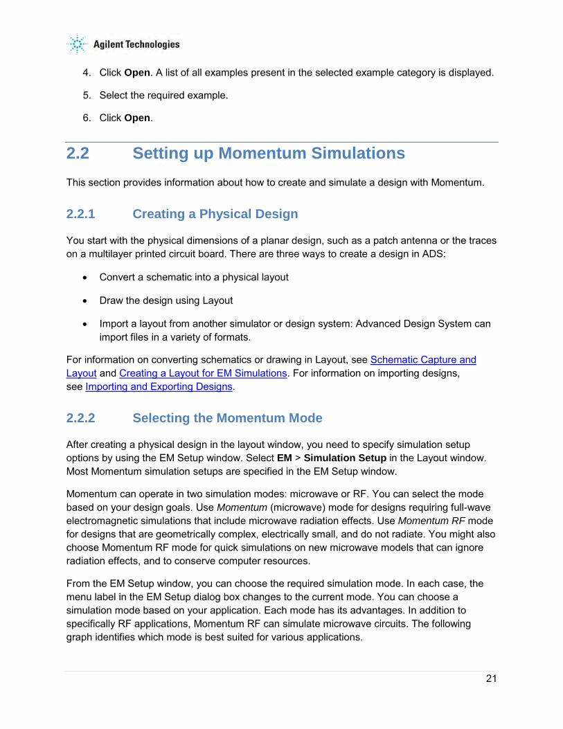
In the EM Setup window, options required for specifying simulation settings are listed in the left pane. You can select the required option to open the settings in the right pane of the EM Setup window, as shown in the following figure:
23
You can specify settings for the following options:
• Layout: You can view information about the workspace, library, cell, and view by selecting Layout. For more information, refer Viewing Layout Information.
• Substrate: You can open a predefined substrate file from ADS by selecting Substrate. For more information, refer Defining Substrates in EM Simulations.
• Ports: You can refresh layout pins information, create, delete, and resequence ports, and search the required S-parameter ports or layout pins by selecting Ports. For more information, refer to Defining Ports in EM Simulations.
• Frequency Plan: You can add or remove frequency plans for your EM simulations by selecting Frequency Plan. For more information, see Defining a Frequency Plan.
• Output Plan: You can specify the data display settings for your EM simulations by selecting Output Plan. For more information, see Defining a Frequency Plan.
• Options: You can define the preprocessor, mesh, simulation, and expert settings by selecting Options. For more information, see Defining Simulation Options.
Electromagnetic
24
• Resources: You can specify the local, remote, and third party settings by selecting Resources. For more information, see Specifying Simulation Resources
• Model/Symbol: You can generate an EM model and symbol by selecting Model/Symbol. For more information, see Generating an EM Model and Symbol.
• Notes: You can add comments to your EM Setup window by selecting Notes.
2.2.4 Defining Substrates
A substrate is the media where a circuit resides. For example, a multilayer PC board consists of various layers of metal, insulating or dielectric material, and ground planes. Other designs may include covers, or they may be open and radiate into air. A complete substrate definition is required in order to simulate a design. The substrate definition includes the number of layers in the substrate and the composition of each layer. This is also where you position the layers of your physical design within the substrate, and specify the material characteristics of these layers.
For specifying a substrate for your Momentum simulation, see Defining Substrates in an EM Simulation.
2.2.5 Assigning Port Properties
Ports enable you to inject energy into a circuit, which is necessary in order to analyze the behavior of your circuit. You apply ports to a circuit when you create the circuit, and then assign port properties in Momentum. There are several different types of ports that you can use in your circuit, depending on your application.
For assigning ports in a Momentum simulation, see Defining Ports in EM Simulations.
2.2.6 Defining the Frequency and Output Plan
You can set up multiple frequency plans for a Momentum simulation. You can also specify the data display settings for your EM simulations by using the EM Setup Window.
For specifying a frequency and output plan, see Defining a Frequency Plan and Defining an Output Plan.
25
2.2.7 Defining Simulation Options
You can specify global options, such as physical model, preprocessor, and mesh for Momentum simulations. You can either use a predefined set of simulation options or or create a new set in Simulation Options of the EM Setup window. You can specify the following simulation options for a Momentum simulation:
• Defining Preprocessor Settings
• Specifying Physical Model Settings for Momentum
• Defining Solver Settings
• Defining Mesh Settings for Momentum
2.2.8 Setting up Local, Remote, or Third Party Simulation
You can run a Momentum simulation on a local or remote machine, or take advantage of a third party load balancing and queuing system such as LSF, Sun Grid Engine, and PBS Professional.
For more information, see Specifying Simulation Resources.
2.2.9 Adding a Box or Waveguide
These elements enable you to specify boundaries on substrates along the horizontal plane. Without a box or waveguide, the substrate is treated as being infinitely long in the horizontal direction. This treatment is acceptable for many designs, but there may be instances where a boundaries need to be taken into account during the simulation process. A box specifies the boundaries as four perpendicular, vertical walls that make a box around the substrate. A waveguide specifies two vertical walls that cut two sides of the substrate. For more information, see Adding Boxes, Waveguides, and Symmetry Planes.
2.2.10 Running the Momentum Simulation
You set up a simulation by specifying the parameters of a frequency plan, such as the frequency range of the simulation and the sweep type. When the setup is complete, you run the simulation. The simulation process uses the mesh pattern, and the electric fields in the design are calculated. S-parameters are then computed based on the electric fields. If the Adaptive

Electromagnetic
26
Frequency Sample sweep type is chosen, a fast, accurate simulation is generated, based on a rational fit model.
For more information, see Running Momentum Simulations.
2.2.11 Viewing Momentum Simulation Results
You can display the results of a Momentum simulation by using the Data Display and Visualization window. You can display the various type of results from a Momentum simulation such as S-parameters, radiation patterns (far-field plots) and derived antenna parameters.
For more information, see Visualizing 3D View before EM Simulation and Visualizing Momentum Simulations.
2.2.12 Computing Radiation patterns
Once the electric fields on the circuit are known, you can compute electromagnetic fields. The electromagnetic fields can be expressed in the spherical coordinate system attached to your circuit. For more information on radiation patterns, see Computing Radiation Patterns.
2.3 Examples- Setting up Momentum Simulations • Designing a Coplanar Waveguide Bend
• Defining Momentum Settings for LPF
2.3.1 Defining Momentum Settings for LPF
This example describes the recommended settings for Momentum by designing a MMIC Low Pass Filter (LPF).
Application Workspace
This application is available in the following location: $HPEESOF_DIR/examples/Tutorial/LPF_Design_Demo_wrk.7zap
Defining a Substrate
To open a predefined substrate:
1. Select EM > Simulation Setup to open the EM Setup window.
2. Select Substrate.
27
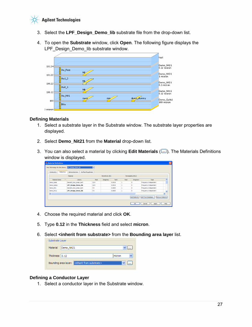
3. Select the LPF_Design_Demo_lib substrate file from the drop-down list.
4. To open the Substrate window, click Open. The following figure displays the LPF_Design_Demo_lib substrate window.
Defining Materials 1. Select a substrate layer in the Substrate window. The substrate layer properties are
displayed.
2. Select Demo_Nit21 from the Material drop-down list.
3. You can also select a material by clicking Edit Materials ( ). The Materials Definitions window is displayed.
4. Choose the required material and click OK.
5. Type 0.12 in the Thickness field and select micron.
6. Select <inherit from substrate> from the Bounding area layer list.
Defining a Conductor Layer 1. Select a conductor layer in the Substrate window.
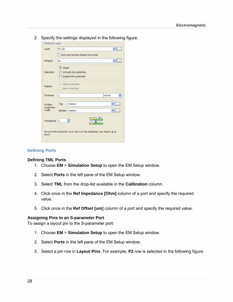
Electromagnetic
28
2. Specify the settings displayed in the following figure:
Defining Ports
Defining TML Ports 1. Choose EM > Simulation Setup to open the EM Setup window.
2. Select Ports in the left pane of the EM Setup window.
3. Select TML from the drop-list available in the Calibration column.
4. Click once in the Ref Impedance [Ohm] column of a port and specify the required value.
5. Click once in the Ref Offset [um] column of a port and specify the required value.
Assigning Pins to an S-parameter Port To assign a layout pin to the S-parameter port:
1. Choose EM > Simulation Setup to open the EM Setup window.
2. Select Ports in the left pane of the EM Setup window.
3. Select a pin row in Layout Pins. For example, P2 row is selected in the following figure:

29
4. Drag the pin from Layout Pins and drop it on the or terminal of the required port in S-parameter Ports. For example, P2 is dragged and dropped on the - terminal of Port1 in the following figure:
5. A message box is displayed if your target pin is already used by other ports.
6. Click Delete Ports and Continue in the message box.
Note You can drag and drop multiple layout pins and connect with a S-parameter port.
Specify a Frequency Plan
To add a frequency plan:
1. Choose EM> Simulation Setup to display the EM Setup window.
2. Select Frequency Plan in the left pane of the EM Setup window.
3. To add a new frequency plan, click Add.
4. Select Adaptive sweep from the Type column.
5. Specify 0 GHz in the Fstart column.

Electromagnetic
30
6. Specify 10 GHz in the Fstop column.
7. Specify 50(max) of N points in the Npts column.
8. Do not specify any value in the Step column.
9. Select the check box in the Enabled column to enable the frequency plan. The following figure displays the recommended frequency settings:
See frequency plan for more information.
Defining an Output Plan
To create an output plan:
1. Choose EM> Simulation Setup to display the EM Setup window.
2. Select Output Plan in the left pane of the EM Setup window.
3. The default dataset name is displayed. To specify a new dataset, click Edit. For more information, see Defining an Output Plan#Selecting an Output Dataset.
4. Select Simulation Type as an appending text to the dataset name.
5. Select Open data display when simulation completes.
6. Select Auto-select based on number of Ports as a template to be used for displaying the data in Template.
7. Select Reuse files from previous simulation.
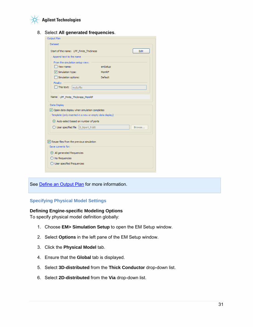
31
8. Select All generated frequencies.
See Define an Output Plan for more information.
Specifying Physical Model Settings
Defining Engine-specific Modeling Options To specify physical model definition globally:
1. Choose EM> Simulation Setup to open the EM Setup window.
2. Select Options in the left pane of the EM Setup window.
3. Click the Physical Model tab.
4. Ensure that the Global tab is displayed.
5. Select 3D-distributed from the Thick Conductor drop-down list.
6. Select 2D-distributed from the Via drop-down list.

Electromagnetic
32
7. Select the required lumped and wire via model options, as shown in the following figure:
Specifying Layer-specific Modeling Options To specify physical model definition for a specific layer:
1. Select EM> Simulation Setup to open EM Setup window.
2. Select Options in the left pane of the EM Setup window.
3. Click the Physical Model tab.
4. Click the Layer Specific tab.

33
5. Select a value from the Model Type for Via drop-down list in the required layer, as shown in the following figure:
Defining Preprocessor Settings
To specify preprocessor settings:
1. Choose EM > Simulation Setup to open the EM Setup window.
2. Select Options in the EM Setup window.
3. Click the Preprocessor tab.
4. Select Heal the layout.
5. Select Auto-determine a safe snap distance (conservative).
6. Select Merge shapes touching each other where possible to preserve the edges shared between adjacent shapes.
7. Select Simplify the layout to generate a conformal mesh containing minimum number of edges.
8. Type 1 in the Displacement field.
9. Select Generate and replace shapes on derived layers to enable the processing of derived layers.

Electromagnetic
34
10. Select Save Preprocessor Messages as a DRC Result to display the location-bound information and warning messages.
11. Type EmPpmsgs in the Job Name field.
12. Type 255 in the DRC Layer field. The following figure displays the recommended preprocessor settings for Momentum.
Defining Mesh Settings
Define global and layer-specific mesh settings for Momentum.
Defining Global Mesh Parameters
Global mesh parameters affect the entire circuit. To set up global parameters:
1. Select EM> Simulation Setup to open the EM Setup window.
2. Select Momentum as the EM simulator.
3. Select Options in the left pane of the EM Setup window.
35
4. Select the Mesh tab. By default, the Global parameters are displayed.
5. Select Highest Simulation Frequency.
6. Select Cell/Wavelength and type 20.
7. Enable Edge Mesh
8. Select Auto-determine Edge Width.
9. Enable Mesh reduction to obtain an optimal mesh with fewer small cells and an improved memory usage and simulation time.
10. Enable Thin layer overlap extraction to extract objects for the following situations:
o Two objects on different layers overlap.
o The objects are separated with a thin substrate layer. If this is enabled, the geometry will be altered to produce a more accurate model for the overlap region. The Normal setting is recommended for most layouts. The Aggressive setting is only recommended when tiny overlap differences are expected to lead to significant result variations as this option will considerably increase the problem size. For more information, refer to Defining Mesh Settings for Momentum#Processing Object Overlap.
Note This should always be enabled for modeling thin layer capacitors.
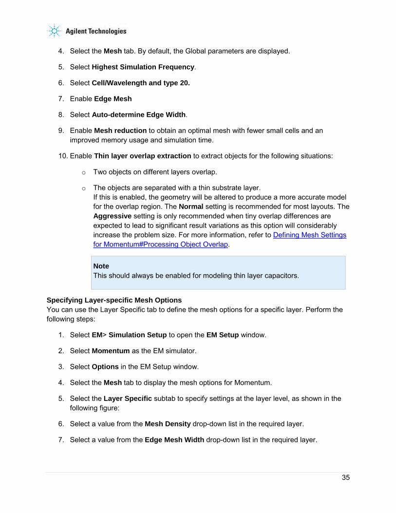
Specifying Layer-specific Mesh Options You can use the Layer Specific tab to define the mesh options for a specific layer. Perform the following steps:
1. Select EM> Simulation Setup to open the EM Setup window.
2. Select Momentum as the EM simulator.
3. Select Options in the EM Setup window.
4. Select the Mesh tab to display the mesh options for Momentum.
5. Select the Layer Specific subtab to specify settings at the layer level, as shown in the following figure:
6. Select a value from the Mesh Density drop-down list in the required layer.
7. Select a value from the Edge Mesh Width drop-down list in the required layer.

Electromagnetic
36
8. Select a value from the Transmission Line Mesh Width drop-down list in the required layer.
Specifying Shape-specific Mesh Options You can customize the selected shape by using the Shape Specific tab. Perform the following steps:
1. Choose EM> Simulation Setup to open the EM Setup window.
2. Select Momentum as the EM simulator.
3. Select Options in the left pane of the EM Setup window.
4. Select the Mesh tab to display the mesh options for Momentum.
5. Select the Shape Specific subtab to specify settings at the shape level, as shown below.
Note To enable the shape-specific options, you need to select a shape in the layout before specifying the options.
6. Enable the Override Layer Specific Mesh Density section. You can select one of the following options:
o Select Maximum Cellsize. Set the maximum value of the mesh density that will be simulated. For more information, refer to Defining Mesh Settings for Momentum#Adjusting Mesh Density.
o Type the number of cells per wavelength in the Cells/Wavelength text box.
7. Enable Override Layer Specific Edge Mesh. You can select one of the following options:
o No Edge Mesh
o Auto-determine Edge Width
o Use Edge Width
8. Enable the Override Layer Specific Transmission Line Mesh section. You can select one of the following options:
o No Transmission Line Mesh
o Cells in Width

37
Creating an EM Model and Symbol
To create an EM model and symbol:
1. Choose EM > Simulation Setup to open the EM Setup window.
2. Select Model/Symbol in the left pane of the EM Setup window.
3. Accept the default emModel name.
4. Select Include S-Parameter data only.
5. Select Create EM Model when simulation is launched. If the Create Now button is labeled Update Now, then the EM Model already exists for this cell.
6. Type Symbol_look_alike in the View Name field.
7. Select Layout Look-alike.
8. Select min pin-pin distance from the Size drop-down list.
9. Select Create Symbol when simulation is launched to create a symbol after the simulation process.
2.3.2 Designing a Coplanar Waveguide Bend
There are two methods for constructing a coplanar waveguide in layout:
• The objects that you draw are the slots on a groundplane. In the substrate definition, the layout layer that the slots are drawn on is mapped to a slot metallization layer.This

Electromagnetic
38
method gives you infinite grounds on the coplanar plane. An example is the coplanar waveguide bend, shown below.
• The objects that you draw represent metal. For example, you can draw strips and ground metal with gaps in between. This layer is mapped to a metallization layer defined as a strip. This method gives you finite grounds on the coplanar plane. Typically, this method is used when coupled microstrip lines are created initially as schematic elements.
Drawing slots on a ground plane is the preferred method because a mesh with fewer edges or unknowns will result, compared to meshing the strips. If a coplanar waveguide design is drawn with strips, it can be converted to a slot pattern with a boolean operation if a bounding box is provided.
Designing a Coplanar Waveguide Bend
This exercise, like the previous exercises, takes you through all of the steps that are necessary when designing with Momentum: creating a layout, defining a substrate, adding ports to the circuit, defining a mesh, simulating, and viewing results. Unlike the previous exercises, this one explores the following design topics:
• Creating a layout that is drawn on more than one layer
• Using vias as connections between layers
• Specifying new port types

39
• Working with new mesh parameters This circuit drawn in this exercise is a coplanar waveguide bend. A coplanar waveguide is, generally, slots filled with a dielectric or air, surrounded by metal, as shown in the figure here.
Creating the Layout
In this example, the circuit is created entirely within the Layout window, and a schematic representation is not used. Be sure to save your work periodically. The layout consists of the following components:
• Coplanar waveguide slots
• Bridges that span the two slots
• Vias that vertically connect the bridges to the slots The slots will be drawn on one layer, the bridges will be drawn on a second layer, and the vias on a third layer. This will be important for when these layers are mapped to the substrate. An illustration of the circuit is shown on the left, the layout is on the right.
Electromagnetic
40
1. Set your preferences so that a Layout window will open instead of a Schematic window. From the Main window, choose Tools > Preferences and enable Create Initial Layout Window. Disable Create Initial Schematic Window.
2. Create a new workspace named cpw_bend.
3. From the Layout window, choose Options > Preferences. Scroll to the Layout Units tab. Set the layout units to um and the resolution to 0.001. Click OK.
4. There is a difference between the length units that you chose when you created the new project, and the units that you just set. The units chosen when you created the project set the units of the layout window in which you are working. The units chosen through Options > Preferences sets the units for objects that are drawn in the Layout window.
5. You will rename the layout layers that are used for drawing the slots, bridges, and vias of the coplanar waveguide bend. Using more descriptive names can help identify which layer that each part of the circuit is drawn on. Choose Options > Layers. Select the Advanced tab. From the Layers list, select cond. In both the Name and Layer Binding fields, enter slot. Click Apply (located just below the Layers list). Select cond2. In both the Name and Layer Binding fields, enter bridge. Click Apply. Select hole. In the Name field only, enter via and click Apply. Click OK.
Drawing the Waveguide Slots
The section describes how to draw the coplanar waveguide slots.
1. Verify that slot is the current layer. The slots will be drawn on this layer. The name of the current layer is displayed in the tool bar and at the top of the Layout window. If slot is not displayed, select it from the list.
2. Choose Insert > Rectangle , then choose Insert > Coordinate Entry. The toolbar arrow is activated and the Coordinate Entry dialog box opens.
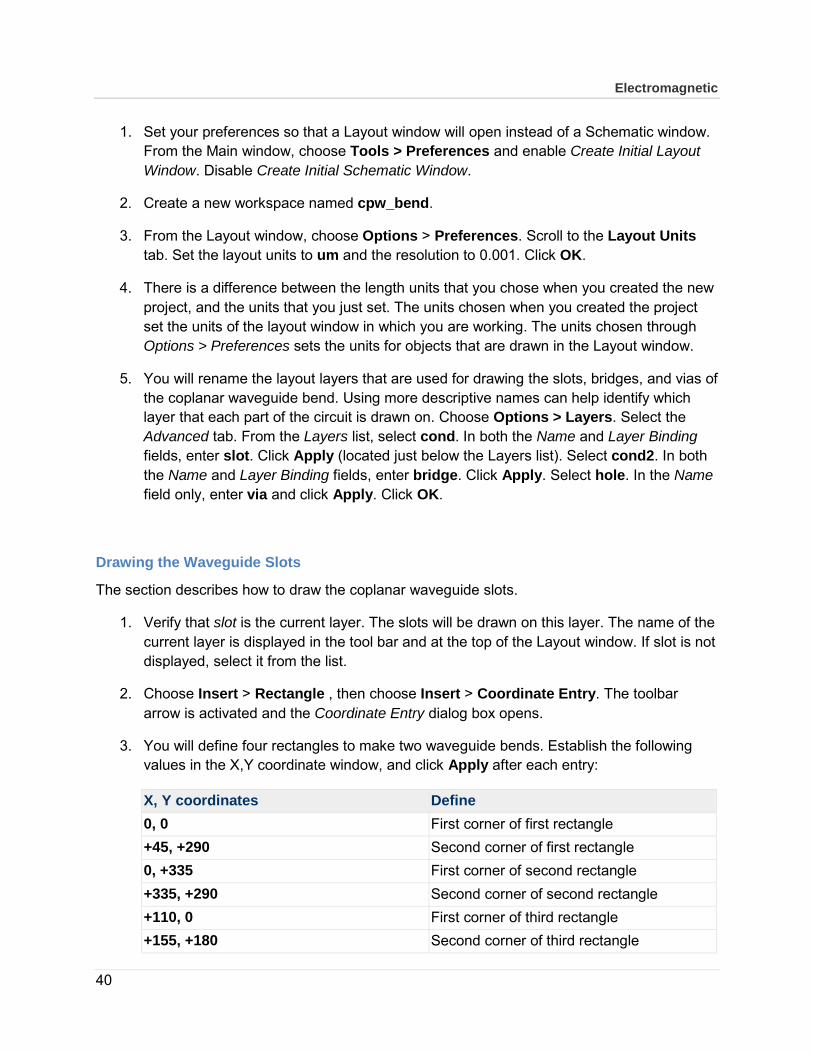
3. You will define four rectangles to make two waveguide bends. Establish the following values in the X,Y coordinate window, and click Apply after each entry:
X, Y coordinates Define 0, 0 First corner of first rectangle +45, +290 Second corner of first rectangle 0, +335 First corner of second rectangle +335, +290 Second corner of second rectangle +110, 0 First corner of third rectangle +155, +180 Second corner of third rectangle
41
X, Y coordinates Define +110, +180 First corner of fourth rectangle +335, +225 Second corner of fourth rectangle
4. Click OK when finished, to dismiss the dialog box.
5. Select View > View All to see your drawing.
6. End the command. The drawing in the layout window should resemble the figure here.
Drawing the Bridges
The slots that make up the coplanar waveguide have been drawn on the layer slot. On a different layer, you will draw the bridges that span the two slots. This is important, because the slots and bridges will be treated differently in Momentum. This will become more clear when the substrate is applied to the circuit, later in this exercise.
1. From the layer list on the toolbar, select the layer bridge and click OK.
Note The slot layer is still visible. You will not do so here, but it can be made invisible if you go to the Layout window and choose Options > Layers , select the slot layer and deselect Vis to turn Visible off. The same action can be taken in Layers window by deselecting Vis in the slot layer.
2. Choose Insert > Rectangle , then choose Insert > Coordinate Entry.
3. Using the Coordinate Entry dialog box you will define two rectangles that make the bridges. Establish the following values in the X,Y coordinate window, and click Apply after each entry:

Electromagnetic
42
X, Y coordinates Define 0, +170 First corner of first bridge +155, +180 Second corner of first bridge +155, +180 First corner of second bridge +165, +335 Second corner of second bridge
4. Click OK when finished, to dismiss the dialog box.
5. End the current command. The drawing in the Layout window should now look like the following figure.
Drawing a Via
The vias must be drawn on a third layer. This is necessary for when the vias are mapped to the substrate, later in this exercise.
The position and size of a via is very important. The various snap modes in Layout can aid in drawing vias, as shown in this part of the exercise. More information on how to draw vias and other drawing tips are in Drawing Tips.
1. From the layout layer list on the toolbar, select via.
2. Choose Options > Preferences. Select the Grid/Snap tab. Under Active Snap Modes, enable Vertex and deselect Grid. Click OK. By using the vertex snap mode, the vias that you draw will snap to the vertex of a nearby object (a bridge) and not to a grid point. This ensures that the vias will be positioned precisely on the edges of the rectangles.
3. Choose Insert > Polyline. Referring to the points identified on the drawing below, create the line segments shown by performing these steps:
o Click once on A1 and click twice on A2.
o Click once on B1 and click twice on B2.

43
o Click once on C1, click once on C2, and click twice on C3. Then, click the toolbar arrow. End the command. The drawing in the Layout window should now appear as shown below.
Opening a Substrate
This exercise uses a substrate that is supplied with Momentum. It will not be necessary to make any changes to it, but it will be reviewed to clarify how layout layers can be mapped to a substrate.
1. From the Layout window, choose EM > Simulation Setup.
2. Select Substrate.
3. Select the substrate file cpw_bend_example.
4. Click Open.
Map the conductor layers 1. Right-click a layer and select Map Conductor Layer. You can see how the layers are
mapped between the Free_Space, air, and GaAs layers:
o There is a thin layer of air between the bridges and the slots.
o The vias are mapped directly to the air substrate layer. The vias, although drawn as lines, are extruded by Momentum and effectively cut vertically through this layer of air, connecting the edges of the slots and the bridges.
o A strip defines the layer such that the bridges are metal and what surrounds the microstrips on that layer is air. A slot is the opposite of a strip: the layout layer would be treated as a ground plane, and the bends that you have drawn are treated as open areas in the ground plane. Vias represent vertical sections that cut through other layers vertically.

Electromagnetic
44
Adding Ports
This section describes how to add ports to the layout and how to apply the coplanar port type to them. Coplanar is one of the several port types that are available in Momentum. It is designed specifically for coplanar waveguide circuits, where an electric field is likely to build up between two ports. Each of the two ports is excited with the same absolute electrical field, but with opposite polarity. The currents are equal but in opposite in direction. For more information, see Using Ports in Momentum.
1. The ports must be added to the waveguide slots and so they must be drawn on the same layer as the slots. From the Layout Layers list box, select slot.
2. The ports must also be positioned in the center of each slot edge. To help position the ports, set the following snap modes:
o Enable Options > Midpoint Snap
o Enable Options > Edge/Centerline Snap
o Disable all other snap modes except Snap Enabled.
3. Click the Pin icon. The Properties dialog box appears.
4. Verify that Num=1. If it is not, select Num and set it to 1. Click OK.
5. Note the ghost image of the port. If it appears very large, or if it cannot be seen, cancel the command. Depending on your system defaults, you may need to change the value of the Port/Ground Size ( Options > Preferences > Placement ) and the value of the Font Definition Size ( Options > Preferences > Component Text) before your ports and labels will be an appropriate size for this layout.
6. When you are ready to add ports, apply them in the order and direction as shown here, then end the port command.

45
7. From the Layout window, chose EM > Simulation Setup. Select Ports to display port properties.
8. In the Layout window, click P1. In the EM Setup window, verify that the calibration is set to TML.
9. Click P2. Verify that the calibration is set to TML.
10. Select the terminal of P2 and drop it on the terminal of P1.
11. Click P3. Verify that the calibration is set to TML.
12. Click P4. Verify that the calibration is set to TML.
13. Select the terminal of P3 and drop it on the terminal of P3.
14. Save your changes.
Generating the Mesh
This section describes how to use additional mesh parameters. Because this circuit is on multiple layers, it is possible to set mesh parameters for each layer. Thus, you can set a relatively dense mesh on a specific layer. In this example, you will not use an edge mesh on the bridge layer.
1. From the Layout window, choose EM > Simulation Setup.
2. Select Options.
3. Click the Mesh tab.
4. Set the following Global parameters:
o Mesh Frequency = 40 GHz
o Number of Cells per Wavelength = 30
o Enable Edge Mesh Global parameters will be applied to all layers, unless other values are specified from the Layer tab.
5. Click the Layer tab.
6. In the Layout Layers list, select bridge. Set the mesh density to 30 and select No Edge Mesh. These mesh parameters will be applied to the objects drawn on the bridge layer only.
7. Select Preprocessed geometry from the Generate list

Electromagnetic
46
8. Click Simulate to start the computations. The mesh will be computed and displayed on the layout, as shown here. Zoom in for a closer look at the mesh.
9. Zoom in on the ports. You can see that additional arrows have been added to each port. The new arrow indicate the direction of the voltage over the slot.
Performing a Simulation
1. From the Layout window, choose EM > Simulation Setup.
2. Select Frequency Plan in the EM Setup window.
3. From the Type list, select Adaptive and set these parameters:
o Fstart = 1 GHz
o Fstop = 40 GHz
o Npts = 50
4. Click Add.
5. Click Simulate.
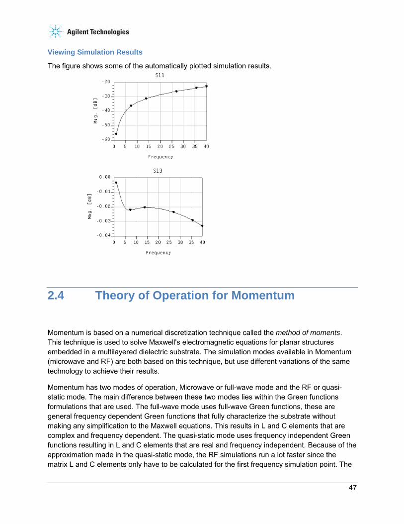
47
Viewing Simulation Results
The figure shows some of the automatically plotted simulation results.
2.4 Theory of Operation for Momentum
Momentum is based on a numerical discretization technique called the method of moments. This technique is used to solve Maxwell's electromagnetic equations for planar structures embedded in a multilayered dielectric substrate. The simulation modes available in Momentum (microwave and RF) are both based on this technique, but use different variations of the same technology to achieve their results.
Momentum has two modes of operation, Microwave or full-wave mode and the RF or quasi-static mode. The main difference between these two modes lies within the Green functions formulations that are used. The full-wave mode uses full-wave Green functions, these are general frequency dependent Green functions that fully characterize the substrate without making any simplification to the Maxwell equations. This results in L and C elements that are complex and frequency dependent. The quasi-static mode uses frequency independent Green functions resulting in L and C elements that are real and frequency independent. Because of the approximation made in the quasi-static mode, the RF simulations run a lot faster since the matrix L and C elements only have to be calculated for the first frequency simulation point. The

Electromagnetic
48
approximation also implies that the quasi-static mode typically should be used for structures that are smaller than half the wavelength. Both engine modes are using the so-called star-loop basis function, ensuring a stable solution at all frequencies. Both engines also make use of a mesh reduction algorithm which reduces the number of unknowns in the simulation by generating a polygonal mesh. This mesh reduction algorithm can be turned on or off, with a toggle switch.
The sources applied at the ports of the circuit yield the excitations in the equivalent network model. The currents in the equivalent network are the unknown amplitudes of the rooftop expansion functions. Solving the equivalent network for a number of independent excitation states yields the unknown current amplitudes. A port calibration process is used to calculate the S-parameter data of the circuit from the current solution, when calibration is requested.
The following sections contain more information about:
• The method of moments technology
• The Momentum solution process
• Special simulation topics
• Considerations and software limitations
2.4.1 The Method of Moments Technology
The method of moments (MoM) technique is based upon the work of R.F. Harrington, an electrical engineer who worked extensively on the method and applied it to electromagnetic field problems, in the beginning of the 1960's. It is based on older theory which uses weighted residuals and variational calculus. More detailed information on the method of moments and Green's theorem refer to, Field Computation by Moment Methods Reference 1).
In the method of moments, prior to the discretization, Maxwell's electromagnetic equations are transformed into integral equations. These follow from the definition of suitable electric and magnetic Green's functions in the multilayered substrate.
In Momentum, a mixed potential integral equation (MPIE) formulation is used. This formulation expresses the electric and magnetic field as a combination of a vector and a scalar potential. The unknowns are the electric and magnetic surface currents flowing in the planar circuit.
Using notations from linear algebra, we can write the mixed potential integral equation in very general form as a linear integral operator equation:
(1)

49
Here, J(r) represents the unknown surface currents and E(r) the known excitation of the problem. The Green's dyadic of the layered medium acts as the integral kernel. The unknown surface currents are discretized by meshing the planar metalization patterns and applying an expansion in a finite number of sub-sectional basis functions B1(r), ..., BN(r):
(2)
The standard basis functions used in planar EM simulators are the subsectional rooftop functions defined over the rectangular, triangular, and polygonal cells in the mesh. Each rooftop is associated with one edge of the mesh and represents a current with constant density flowing through that edge as shown in the following illustration. The unknown amplitudes Ij, j=1,..,N of the basis function expansion determine the currents flowing through all edges of the mesh.
Discretization of the surface currents using rooftop basis functions.
The integral equation (1) is discretized by inserting the rooftop expansion (2) of the currents. By applying the Galerkin testing procedure, that is, by testing the integral equation using test functions identical to the basis functions, the continuous integral equation (1) is transformed into a discrete matrix equation:
for i=1,...,N
(3)
with
(4)
(5)

Electromagnetic
50
The left hand side matrix [Z] is called the interaction matrix, as each element in this matrix describes the electromagnetic interaction between two rooftop basis functions. The dimension N of [Z] is equal to the number of basis functions. The right-hand side vector [V] represents the discretized contribution of the excitations applied at the ports of the circuit.
The surface currents contribute to the electromagnetic field in the circuit by means of the Green's dyadic of the layer stack. In the MPIE formulation, this Green's dyadic is decomposed into a contribution from the vector potential A(r) and a contribution from the scalar potential V(r):
(6)
The scalar potential originates from the dynamic surface charge distribution derived from the surface currents and is related to the vector potential through the Lorentz gauge. By substituting the expression (6) for the Green's dyadic in the expression (4) for the interaction matrix elements, yields the following form:
(7)
with
(8)
(9)
This allows the interaction matrix equation to be given a physical interpretation by constructing an equivalent network model. In this network, the nodes correspond to the cells in the mesh and hold the cell charges. Each cell corresponds to a capacitor to the ground. All nodes are connected with branches which carry the current flowing through the edges of the cells. Each branch has in inductor representing the magnetic self coupling of the associated current basis function. The equivalent circuit is built by replacing each cell in the mesh with a capacitor to the ground reference and inductors to the neighboring cells, as shown in the following figure:
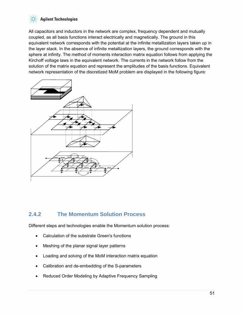
51
All capacitors and inductors in the network are complex, frequency dependent and mutually coupled, as all basis functions interact electrically and magnetically. The ground in this equivalent network corresponds with the potential at the infinite metallization layers taken up in the layer stack. In the absence of infinite metallization layers, the ground corresponds with the sphere at infinity. The method of moments interaction matrix equation follows from applying the Kirchoff voltage laws in the equivalent network. The currents in the network follow from the solution of the matrix equation and represent the amplitudes of the basis functions. Equivalent network representation of the discretized MoM problem are displayed in the following figure:
2.4.2 The Momentum Solution Process
Different steps and technologies enable the Momentum solution process:
• Calculation of the substrate Green's functions
• Meshing of the planar signal layer patterns
• Loading and solving of the MoM interaction matrix equation
• Calibration and de-embedding of the S-parameters
• Reduced Order Modeling by Adaptive Frequency Sampling

Electromagnetic
52
Calculation of the Substrate Green's Functions
The substrate Green's functions are the spatial impulse responses of the substrate to Dirac type excitations. They are calculated for each pair of signal (strip, slot and/or via) layers mapped to a substrate level. Although it is necessary to know which signal layers are mapped to a substrate level, since only impulse responses are being calculated, it is not necessary to know the patterns on these signal layers. This implies that the Green's functions can be pre-calculated and stored in a substrate database. This allows the substrate Green's functions to be reused for other circuits defined on the same substrate.
The high frequency electromagnetic Green's functions depend upon the radial distance and the frequency. The computations are performed up to very large radial distances over the entire frequency band specified by the user. The frequency points are selected adaptively to ensure an accurate interpolation with respect to frequency. Computations performed over very wide frequency ranges can consume more CPU time and disk space to store the results. To increase speed, the RF mode uses quasi-static electromagnetic Green's functions based on low-frequency approximation and scales the quasi-static Green functions at higher frequencies.
Meshing of the Planar Signal Layer Patterns
The planar metallization (strip, via) and aperture (slot) patterns defined on the signal layers are meshed with rectangular and triangular cells in the microwave simulation mode. As translational invariance can be used to speed up the interaction matrix load process, the meshing algorithm will maximize the number of uniform rectangular cells created in the mesh. The meshing algorithm is very flexible as different parameters can be set by the user (number of cells/wavelength, number of cells/width, edge meshing, and mesh seeding), resulting in a mesh with different density. It is clear that the mesh density has a high impact on both the efficiency and accuracy of the simulation results. Default mesh parameters are provided which give the best accuracy/efficiency trade-off. Both the RF and microwave modes use mesh reduction technology to combine rectangular and triangular cells to produce a mesh of polygonal cells, thus reducing demand for computer resources. Mesh reduction eliminates small rectangles and triangles which from an electrical modeling point of view only complicate the simulation process without adding accuracy. As mentioned previously, this feature may be turned on or off with a toggle switch.
Loading and Solving of the MoM Interaction Matrix Equation
The loading step of the solution process consists of the computation of all the electromagnetic interactions between the basis functions and the filling of the interaction matrix and the excitation vector. The interaction matrix as defined in the rooftop basis is a dense matrix, that is,
53
each rooftop function interacts with every other rooftop function. This electromagnetic interaction between two basis functions can either be strong or weak, depending on their relative position and their length scale. The matrix filling process is essentially a process of order (N2), (i.e. the computation time goes up with the square of the number of unknowns).
In the solving step, the interaction matrix equation is solved for the unknown current expansion coefficients. The solution yields the amplitudes of the rooftop basis functions which span the surface current in the planar circuit. Once the currents are known, the field problem is solved because all physical quantities can be expressed in terms of the currents. With the release 2005A, an iterative matrix solve scheme was introduced in Momentum. For large problem sizes, the iterative matrix solve performs as an order (N2) process. Momentum still uses a direct matrix solve process if the structure is small or when convergence problems are detected in the iterative matrix solver process.
Calibration and De-embedding of the S-parameters
Momentum performs a calibration process on the single type port, the same as any accurate measurement system, to eliminate the effect of the sources connected to the transmission line ports in the S-parameter results. Feedlines of finite length (typically half a wavelength at high frequencies, short lines are used at low frequencies) are added to the transmission line ports of the circuit. Lumped sources are connected to the far end of the feedlines. These sources excite the eigenmodi of the transmission lines without interfering with the circuit. The effect of the feedlines is computed by the simulation of a calibration standard and subsequently removed from the S-parameter data. A built-in cross section solver calculates the characteristic impedance and propagation constant of the transmission lines. This allows to shift the phase reference planes of the S-parameters, a process called de-embedding. Results of the calibration process includes the elimination of low-order mode mismatches at the port boundary, elimination of high-order modes, and removal of all port excitation parasitics.
Besides transmission line ports, Momentum offers the user the ability to define direct excitation or internal ports. These ports can be specified at any location on the planar metallization patterns as either a point or a line feed. They allow to connect both passive and active lumped components to the distributed model of the planar circuits. The S-parameters associated with these ports are calculated from the excitation consisting of a lumped source connected to the equivalent network model at the locations of the internal ports. The parasitic effects of these lumped sources are not calibrated out of the S-parameters results.
Reduced Order Modeling by Adaptive Frequency Sampling
A key element to providing fast, highly accurate solutions using a minimum of computer resources is the Adaptive Frequency Sampling (AFS) technology. When simulating over a large frequency range, oversampling and straight line interpolation can be used to obtain smooth curves for the S-parameters. Oversampling however implies a huge amount of wasted

Electromagnetic
54
resources. Momentum allows the user to benefit from a smart interpolation scheme based on reduced order modeling techniques to generate a rational pole/zero model for the S-parameter data. The Adaptive Frequency Sampling algorithm selects the frequency samples automatically and interpolates the data using the adaptively constructed rational pole/zero model. This feature allows important details to be modeled by sampling the response of the structure more densely where the S-parameters are changing significantly. It minimizes the total number of samples needed and maximizes the information provided by each new sample. In fact, all kinds of structure can take advantage of the AFS module. The Adaptive Frequency Sampling technology reduces the computation time needed for simulating large frequency ranges with Momentum significantly.
2.4.3 Special Simulation Topics
Some special simulation topics are discussed in this section:
• Simulating slots in ground planes
• Simulating metallization loss
• Simulating internal ports and ground references
Simulating Slots in Ground Planes
Slots in ground planes are treated in a special manner by Momentum. An electromagnetic theorem called the equivalence principle is applied. Instead of attempting to simulate the flow of electric current in the wide extent of the ground plane, only the electric field in the slot is considered. This electric field is modeled as an equivalent magnetic current that flows in the slot. Momentum does not model finite ground plane metallization thickness. Ground planes and their losses are part of the substrate definition.
By using slot metallization definitions, entire structures, such as slot lines and coplanar waveguide circuits, can be built. Slots in ground planes can also be used to simulate aperture coupling through ground planes for multi-level circuits. Structure components on opposite sides of a ground plane are isolated from each other, except for intermediate coupling that occurs through the slots. This treatment of slots allows Momentum to simulate slot-based circuits and aperture coupling very efficiently.
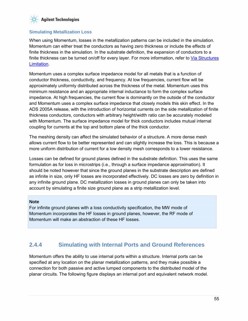
55
Simulating Metallization Loss
When using Momentum, losses in the metallization patterns can be included in the simulation. Momentum can either treat the conductors as having zero thickness or include the effects of finite thickness in the simulation. In the substrate definition, the expansion of conductors to a finite thickness can be turned on/off for every layer. For more information, refer to Via Structures Limitation.
Momentum uses a complex surface impedance model for all metals that is a function of conductor thickness, conductivity, and frequency. At low frequencies, current flow will be approximately uniformly distributed across the thickness of the metal. Momentum uses this minimum resistance and an appropriate internal inductance to form the complex surface impedance. At high frequencies, the current flow is dominantly on the outside of the conductor and Momentum uses a complex surface impedance that closely models this skin effect. In the ADS 2005A release, with the introduction of horizontal currents on the side metallization of finite thickness conductors, conductors with arbitrary height/width ratio can be accurately modeled with Momentum. The surface impedance model for thick conductors includes mutual internal coupling for currents at the top and bottom plane of the thick conductor.
The meshing density can affect the simulated behavior of a structure. A more dense mesh allows current flow to be better represented and can slightly increase the loss. This is because a more uniform distribution of current for a low density mesh corresponds to a lower resistance.
Losses can be defined for ground planes defined in the substrate definition. This uses the same formulation as for loss in microstrips (i.e., through a surface impedance approximation). It should be noted however that since the ground planes in the substrate description are defined as infinite in size, only HF losses are incorporated effectively. DC losses are zero by definition in any infinite ground plane. DC metallization losses in ground planes can only be taken into account by simulating a finite size ground plane as a strip metallization level.
Note For infinite ground planes with a loss conductivity specification, the MW mode of Momentum incorporates the HF losses in ground planes, however, the RF mode of Momentum will make an abstraction of these HF losses.
2.4.4 Simulating with Internal Ports and Ground References
Momentum offers the ability to use internal ports within a structure. Internal ports can be specified at any location on the planar metallization patterns, and they make possible a connection for both passive and active lumped components to the distributed model of the planar circuits. The following figure displays an internal port and equivalent network model.
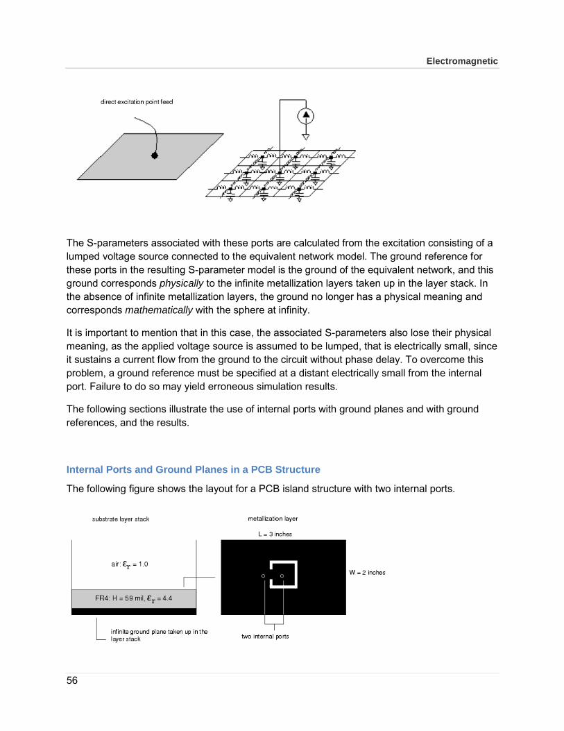
Electromagnetic
56
The S-parameters associated with these ports are calculated from the excitation consisting of a lumped voltage source connected to the equivalent network model. The ground reference for these ports in the resulting S-parameter model is the ground of the equivalent network, and this ground corresponds physically to the infinite metallization layers taken up in the layer stack. In the absence of infinite metallization layers, the ground no longer has a physical meaning and corresponds mathematically with the sphere at infinity.
It is important to mention that in this case, the associated S-parameters also lose their physical meaning, as the applied voltage source is assumed to be lumped, that is electrically small, since it sustains a current flow from the ground to the circuit without phase delay. To overcome this problem, a ground reference must be specified at a distant electrically small from the internal port. Failure to do so may yield erroneous simulation results.
The following sections illustrate the use of internal ports with ground planes and with ground references, and the results.
Internal Ports and Ground Planes in a PCB Structure
The following figure shows the layout for a PCB island structure with two internal ports.

57
The infinite ground plane is taken up in the substrate layer stack and provides the ground reference for the internal ports. The magnitude and phase of the S21-parameter calculated with Momentum. The simulation results are validated by comparing them with the measured data for the magnitude and the phase of S21. h6. The following figure displays the Magnitude and phase of S21:
The thicker line is Momentum results, the thinner line is the measurement.
Finite Ground Plane, no Ground Ports
The same structure was resimulated with a finite groundplane. The substrate layer stack contains no infinite metallization layers. No ground reference was specified for the ports, so the sphere at infinity acts as the ground reference for the internal ports. The S-parameters obtained from a simulation for these ports no longer have a physical meaning. The following figure displays PCB substrate layer stack and metallization layers:
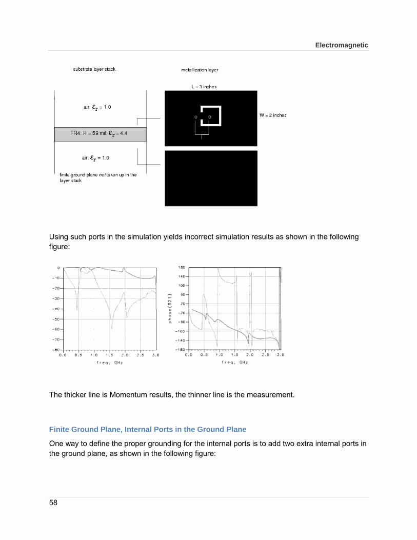
Electromagnetic
58
Using such ports in the simulation yields incorrect simulation results as shown in the following figure:
The thicker line is Momentum results, the thinner line is the measurement.
Finite Ground Plane, Internal Ports in the Ground Plane
One way to define the proper grounding for the internal ports is to add two extra internal ports in the ground plane, as shown in the following figure:
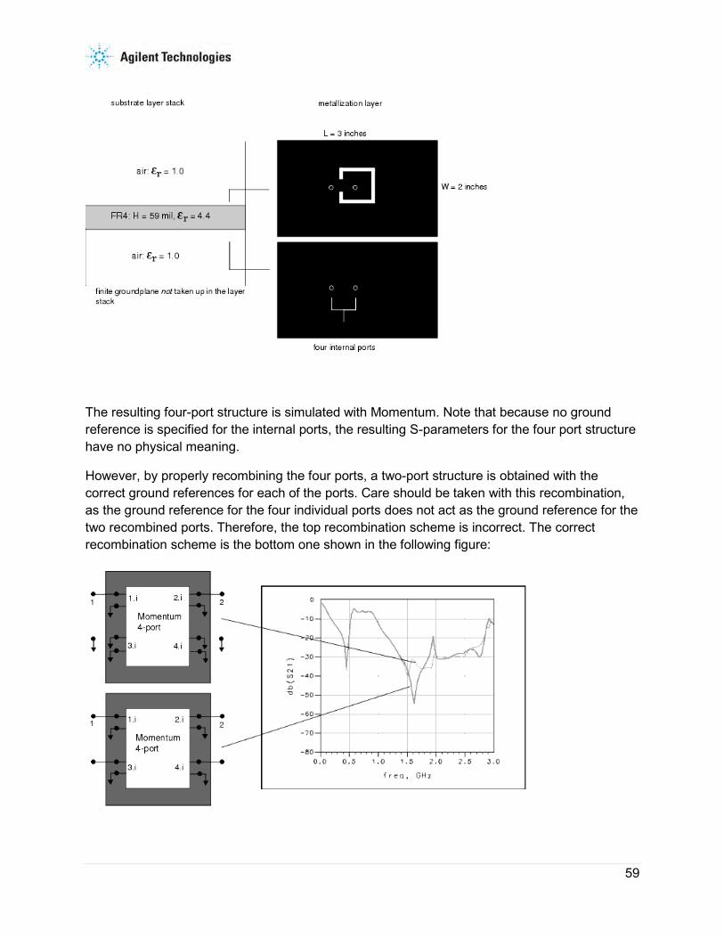
59
The resulting four-port structure is simulated with Momentum. Note that because no ground reference is specified for the internal ports, the resulting S-parameters for the four port structure have no physical meaning.
However, by properly recombining the four ports, a two-port structure is obtained with the correct ground references for each of the ports. Care should be taken with this recombination, as the ground reference for the four individual ports does not act as the ground reference for the two recombined ports. Therefore, the top recombination scheme is incorrect. The correct recombination scheme is the bottom one shown in the following figure:

Electromagnetic
60
Finite Ground Plane, Ground References
The process of adding two extra internal ports in the ground plane and recombining the ports in the correct way can be automated in Momentum by defining two ground reference ports, as shown in the following figure:
The S-parameters obtained with Momentum are identical to the S-parameters of the two-port after the correct recombination in the section above, also shown in the following figure:
The thicker line is Momentum results, the thinner line is the measurement.
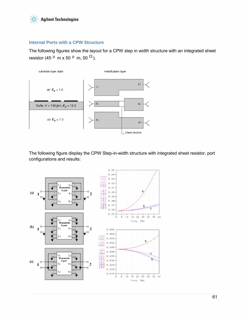
61
Internal Ports with a CPW Structure
The following figures show the layout for a CPW step in width structure with an integrated sheet resistor (45 m x 50 m, 50 ).
The following figure display the CPW Step-in-width structure with integrated sheet resistor, port configurations and results:

Electromagnetic
62
Six internal ports are added to the metallization layers. The six-port S-parameter model is recombined into a two-port model to describe the CPW-mode S-parameters. Different recombination schemes are possible, yielding different simulation results. Scheme (c) is the correct one, as the ground reference for the internal ports is the sphere at infinity and this cannot act as the ground reference for the CPW ports.
The process of adding extra internal ports to the ground metallization patterns and recombining the ports in the correct way can be automated in Momentum by defining ground reference ports, as shown in the following figure:
2.4.5 Limitations and Considerations
This section describes some software limitations and physical considerations which need to be taken into account when using Momentum:
• Comparing the microwave and RF simulation modes
• Matching the simulation mode to circuit characteristics
• Higher-order modes and high frequency limitation
• Substrate waves and substrate thickness limitation
• Parallel-plate modes and high frequency limitation
• Slotline structures and high frequency limitation

63
• Via structures and metallization thickness limitation
• Via structures and substrate thickness limitation
• CPU time and memory requirements
Comparing the Microwave and RF Simulation Modes
Momentum has two simulation modes: the Microwave and RF mode. The Microwave mode uses full-wave formulation, the RF mode uses a quasi-static formulation. In the quasi-static formulation, the Green functions are low-frequency approximations to the full-wave and more general Green functions. Because of the approximations made in the RF mode, the simulations are more efficient. The approximation is valid for structures that are small compared to the wavelength (size of the circuit smaller than half a wavelength).
Note For infinite ground planes with a loss conductivity specification, the MW mode of Momentum incorporates the HF losses in ground planes, however, the RF mode of Momentum will make an abstraction of these HF losses.
Matching the Simulation Mode to Circuit Characteristics
The Momentum RF mode can be used to simulate RF and microwave circuits, depending on your requirements. However, Momentum RF is usually the more efficient mode when a circuit is electrically small, geometrically complex, and does not radiate. This section describes these characteristics.
Radiation Momentum RF provides accurate electromagnetic simulation performance at RF frequencies. However, this upper limit depends on the size of your physical design. At higher frequencies, as radiation effects increase, the accuracy of the Momentum RF models declines smoothly with increased frequency.
Similarly, if the substrate allows the propagation of surface waves (these are guided waves that propagate in the substrate layers) the accuracy of the RF mode will gradually decline because surface waves are not included in the RF calculation.
Electrically Small Circuits Momentum RF works best for electrically small circuits as its accuracy smoothly decreases with increasing electrical size relative to a given frequency. A circuit is considered electrically small

Electromagnetic
64
relative to a given frequency if its physical dimension is smaller than half the wavelength of the frequency. Depending on which value you know, maximum circuit dimension or maximum simulation frequency, you can determine a qualitative approximation of the circuit's electrical size.
For space wave radiation, you can use one of the following two expressions strictly as a guideline to have an awareness about the circuit's electrical size relative to the maximum frequency you plan to run the simulation. When you know the value of D , use the first expression to approximate the maximum frequency up to which the circuit is electrically small. When you know the maximum simulation frequency, use the second expression to approximate the maximum allowable dimension:
or
where: D = the maximum length in mm diagonally across the circuit. F = the maximum frequency in GHz . The following expression provides a guideline up to which frequency the substrate is electrically small for surface wave radiation.
During a simulation, Momentum RF calculates the maximum frequency up to which the circuit is considered electrically small, and displays that value in the status display. This is similar to using the expressions above since the dimension and thickness of a layout is typically fixed, and it is the simulation frequency that is swept.

65
Geometrically Complex Circuits The mesh generated for a simulation establishes a geometric complexity for a circuit. A circuit is considered geometrically complex if its shape does not fit into a uniform, rectangular mesh, and the mesh generation produces a lot of triangles. Layouts containing shapes such as circles, arcs, and non-rectangular polygons usually result in meshes with many triangles. A measure of increasing geometric complexity is when the ratio of triangular cells to rectangular cells grows larger:
The mesh-reduction technology offered by Momentum RF and Microwave eliminates electromagnetically redundant rectangular and triangular cells. This reduces the time required to complete the simulation thus increasing efficiency. This mesh reduction algorithm can be turned on or off, using a toggle switch.
Higher-order Modes and High Frequency Limitation
Since Momentum does not account for higher-order modes in the calibration and de-embedding process, the highest frequency for which the calibrated and de-embedded S-parameters are valid is determined by the cutoff frequency of the port transmission line higher-order modes. As a rule of thumb for microstrip transmission lines, the cutoff frequency (in GHz) for the first higher-order mode is approximately calculated by:
Cutoff frequency fc = 0.4 Z0 / height where Z0 is the characteristic impedance of the transmission line. For a 10 mil alumina substrate with 50 ohm microstrip transmission line, we obtain a high frequency limit of approximately fc = 80 GHz.
Parallel Plate Modes
In the region between two infinite parallel plates or ground planes, parallel plate modes exist. Any current flowing in the circuit will excite all of these modes. How strong a mode will be excited depends on how well the field generated by the current source matches with the field distribution of the parallel plate mode.
A distinction can be made between the fundamental mode and the higher order modes. The fundamental mode, which has no cut-off frequency, propagates at any frequency. The higher order modes do have a cut-off frequency. Below this frequency, they decay exponentially and only influence the local (reactive) field around the source. Above this frequency, they propagate as well and may take real energy away from the source.

Electromagnetic
66
Momentum takes the effect of the fundamental mode into account. The higher order modes are taken into account as long as they are well below cut-off. If this is not the case, a warning is issued saying that higher-order parallel plate modes were detected close to their cut-off frequency. Simulation results will start to degrade from then on.
The Effect of Parallel Plate Modes The fundamental mode has its electric field predominantly aligned along the Z-axis from the top plate to the bottom plate. This means that this mode creates a difference in the potential between both plates. This mode can be excited by any current in your circuit: electric currents on a strip or via, magnetic currents on a slot. It behaves as a cylindrical wave that propagates to infinity where it feels a short circuit (since both plates are connected there). However, since infinity is very far away, no reflected wave ever comes back.
In a symmetric strip line structure, the current on the strip won't excite the fundamental mode due to this symmetry. However, the presence of a feature such as a slot in one of the plates creates an asymmetry. The slot will excite the fundamental mode!
The accuracy of the Momentum results for calibrated ports degrades when the parallel plate modes become important. For calibrated ports is assumed that they excite the circuit via the fundamental transmission line mode. However, this excitation is not pure. The source will excite the circuit via the parallel plate modes, too. This effect cannot be calibrated out, since those contributions are not orthogonal. The consequence is that the excitation doesn't correspond with a pure fundamental transmission line mode excitation.
Avoiding Parallel Plate Modes You can short circuit the parallel plate modes by adding vias to your structure at those places where parallel plate modes will be excited. Similar problems will exist with the measurements. Both plates must be connected explicitly with each other! This won't take place at infinity but somewhere at the side of the board. If no vias are used in the real structure, the fundamental mode may be excited. This mode will propagate to the borders and reflect. Thus, the real structure differs in that from the simulations where no reflection will be seen since a reflection only happens at infinity.
One way to counter the difference between measurements in reality and simulation is to take into account the package (box) around the structure. Another possibility is adding vias to your structure, both in real life and in the simulations. Try to make the physical representation of your circuit as close as possible to reality. However, the actual shape of the via should not be that important. Small sheets can be used to represent the small circular vias that are realized in the real structure.

67
Surface Wave Modes
If the substrate is not closed (open or half open), and not homogeneous, surface wave modes can exist. The parallel plate mode can be seen as a special case of a surface wave mode. Their behavior is identical. Both are cylindrical waves that propagate radially away from the source. They are guided by the substrate. Both fundamental and higher order surface wave modes exist. Similar conclusions can be drawn with respect to limitations such as the effects of the modes.
Slotline Structures and High Frequency Limitation
The surface wave accuracy deterioration of the calibration process is somewhat more prominent for slotline transmission lines than for microstrip transmission lines. Therefore, slotline structures simulated with Momentum will exhibit a somewhat higher noise floor (10-20 dB higher) than microstrip structures. For best results, the highest simulation frequency for slotline structures should satisfy:
Substrate thickness < 0.15 * effective wavelength
Simulation of narrow slot lines are accurate at frequencies somewhat higher than the high frequency limit determined by this inequality, but wide slotlines will show deteriorated accuracy at this frequency limit.
Via Structures Limitation
In Momentum, the current flow on via structures is only allowed in the vertical direction; horizontal or circulating currents are not modeled. As via structures are metallization patterns, the modeling of metallization losses in via's is identical to the modeling of metallization loss in microstrip and slotline structures.
Via Structures and Substrate Thickness Limitation
The vertical electrical currents on via structures are modeled with rooftop basis functions. In this modeling, the vertical via structure is treated as one cell. This places an upper limit to the substrate layer thickness as the cell dimensions should not exceed 1/20 of a wavelength for accurate simulation results. Momentum simulations with via structures passing through electrically thick substrate layers will become less accurate at higher frequencies. By splitting the thick substrate layer into more than one layer, more via-cells are created and a more accurate solution is obtained.
CPU Time and Memory Requirements
Both CPU time and memory needed for a Momentum simulation increase with the complexity of the circuit and the density of the mesh. The size N of the interaction matrix equation is equal to the number of edges in the mesh. For calibrated ports, the number of unknowns is increased with the edges in the feedlines added to the transmission line ports.

Electromagnetic
68
CPU Time The CPU time requirements for a Momentum simulation can be expressed as:
CPU time = A + B N + C N2 + D N3
where:
N = number of unknowns
A, B, C, D = constants independent of N
The constant term A accounts for the simulation set up time. The meshing of the structure is responsible for the linear term, BN. The loading of the interaction matrix is responsible for the quadratic term and the solving of the matrix equation accounts for:
• part of the quadratic term (when using the iterative solver)
• the cubic term (when using the direct solver)
It is difficult to predict the value of the constants A, B, C and D, because they depend on the problem at hand.
Memory Usage The memory requirement for a Momentum simulation can be expressed as:
Memory = X + Y N + Z N2
where
N = number of unknowns
X, Y, Z constants independent of N
Like with the CPU time expression, the constants X, Y and Z are difficult to predict for any given structure.
For medium to large size problems, the quadratic term, which accounts for storing of the interaction matrix, always dominates the overall memory requirement. For small structures, memory usage can also be dependent upon the substrate. The substrate database must be read and interpolated, which requires a certain amount of memory. Algorithms to make trade-off between time and memory resources are implemented in the simulator. These algorithms result in additional usage above that required to solve the matrix. Total memory consumption is typically less than 1.5 times what is required to store the matrix, for large matrices.

69
2.4.6 References
1. R. F. Harrington, Field Computation by Moment Methods . Maxillan, New York (1968).
2.5 Conductor Loss Models in Momentum
2.5.1 Surface Impedance Models
Sheet Conductor
In momentum.cfg file:
MOM3D_USE_SHEETLOSSMODEL=0,1,2
model 0: DC resistance
model 1: single sided skin effect Note: this is default in ADS 2008.
model 2: double sided skin effect
Note: this is default in ADS 2009.
Thick Conductor (no horizontal side currents)
In momentum.cfg file:
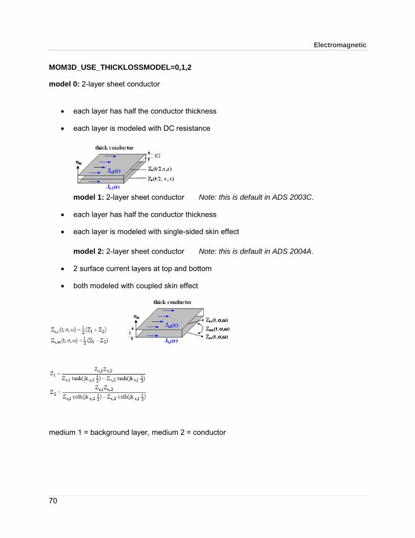
Electromagnetic
70
MOM3D_USE_THICKLOSSMODEL=0,1,2
model 0: 2-layer sheet conductor
• each layer has half the conductor thickness
• each layer is modeled with DC resistance
model 1: 2-layer sheet conductor Note: this is default in ADS 2003C.
• each layer has half the conductor thickness
• each layer is modeled with single-sided skin effect model 2: 2-layer sheet conductor Note: this is default in ADS 2004A.
• 2 surface current layers at top and bottom
• both modeled with coupled skin effect
medium 1 = background layer, medium 2 = conductor

71
Thick Conductor (horizontal side currents included)
The same models as for thick conductors without horizontal side currents apply, however, the thickness is replaced by the effective thickness of the solid object represented by the thick conductor.
2.5.2 Example: Single Trace in Free Space

Electromagnetic
72
Convergence Using N-layer Sheet Conductor Model
Results Using Sheet Conductor Models
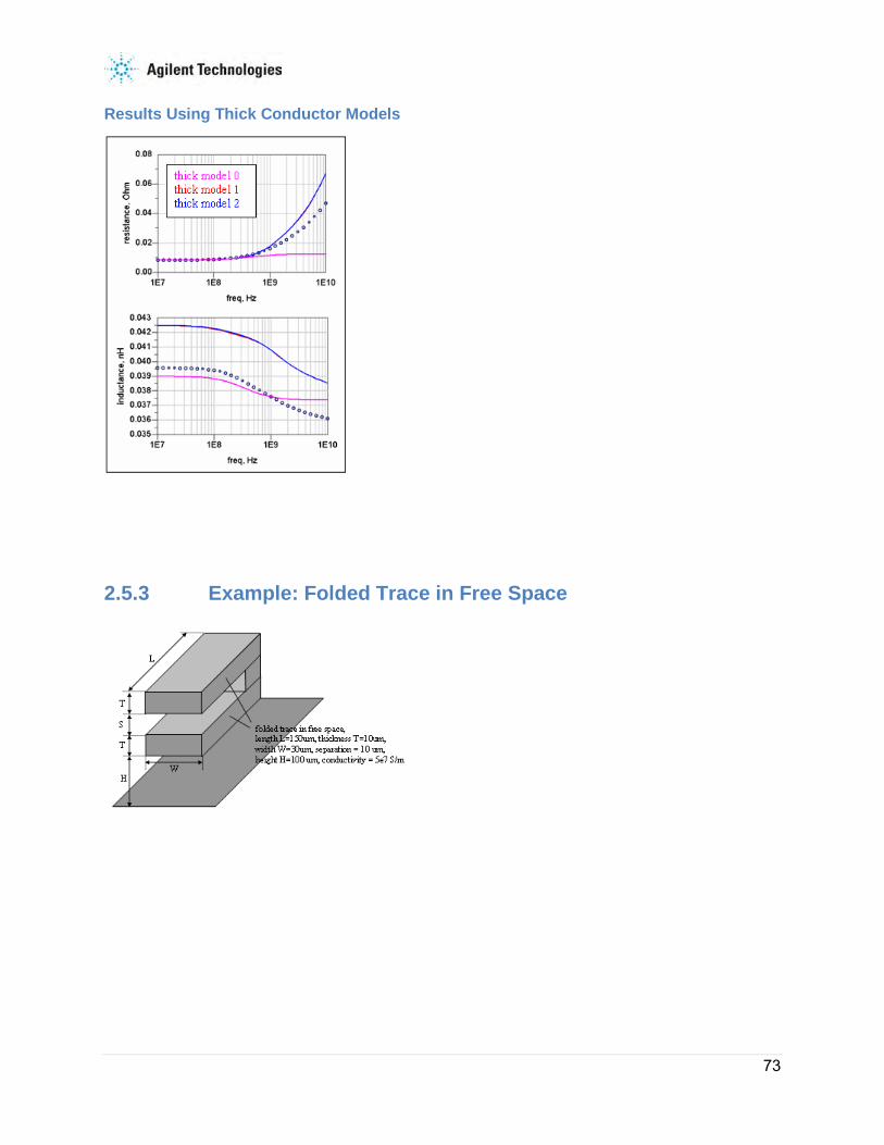
73
Results Using Thick Conductor Models
2.5.3 Example: Folded Trace in Free Space

Electromagnetic
74
Results Using Thick Conductor Models
2.5.4 Using Infinite and Finite Ground Planes
Any closed boundary condition or slot conductor layer in ADS is considered to be an infinite Ground Plane. It is important to understand what is modeled for the various definitions for these infinite planes. Since return currents are modeled in the infinite ground plane for all three models (perfect conductor, impedance, conductivity), the inductance of the Ground Plane is included in the simulation results for any case with an infinite Ground Plane.
When using the impedance and conductivity models for infinite Ground Planes, Momentum and FEM models and captures an equivalent surface impedance. The surface impedance is described as follows:
• For both the impedance and conductivity models, the High Frequency resistive losses are included but not the DC resistive losses.
• For the impedance model, the surface impedance is constant versus frequency.
• For the conductivity model, the surface impedance is frequency dependent. (Note: for infinite ground planes with a loss conductivity specification, the MW mode of Momentum incorporates the High Frequency (HF) losses in ground planes; however, the RF mode of Momentum will make an abstraction of these HF losses.)
If DC resistive losses need to be modeled in a Ground Plane, then a finite Ground Plane must be used. The DC resistance between two points on an infinite ground plane is always zero

75
(independent of the impedance value). This is a theoretical limit that does not exist in real life (ground planes are always finite in size). Hence, Momentum will always compute a zero DC resistance for an infinite Ground Plane.
Specifying a finite conductivity in the Ground Plane provides an additional way to model a loss mechanism that happens in a real world situation. In this case, it is the resistive losses of the 'return current' that flows in the Ground Plane. In most practical cases the Ground Plane losses are much smaller than the losses in the signal lines because the Ground Plane metallization is both thicker and wider than the signal lines (thus the return current is distributed on more metal which reduces the losses). As such, modeling the Ground Plane as a "Perfect Conductor" is less of an approximation than modeling the signal lines as "Perfect Conductors".
Another way to think about this would be to consider the difference between modeling a big chunk of metal (an 'area fill' as a 'finite Ground Plane') as either a "Perfect Conductor" or with a finite conductivity. The effect will typically be a slight increase in the simulated losses, but usually the difference will be pretty small.
Defining Infinite Ground Planes in ADS
This section demonstrates how to define infinite Ground Planes within ADS. When an infinite Ground Plane is required, the ‘Closed’ boundary condition is used. This can be selected at the top and/or bottom of the substrate stack-up. Note that intermediate layers in the substrate stack-up can also be used as infinite Ground Planes, but are defined by using the ‘Layout Layers’ tab of the substrate editor to define ‘Slot’ planes at the desired locations.
Access the substrate editor, to define the ‘Closed’ boundary condition (or ‘Slot’ layers) that is used for an infinite Ground Plane. The Slot layers may also be used as infinite Ground Planes. This can be used in many different applications. Consider the case of a simple transmission line over an infinite Ground Plane that has a hole in it. If you want to create this structure, perform the following the steps in the subsequent Figures.
ADS Momentum Layout for a very simple case of a transmission line over an infinite Ground Plane that has a hole in it. (The signal trace is on the “cond’ layer and the hole for the Ground Plane is drawn on the “resi” layer, which is displayed in green and in outline mode. There is no significance to which layer upon which this is drawn, we just need to make note of it for the next steps.)

Electromagnetic
76
After the layout is created, the next step is to properly define the substrate stack-up. This is shown in the next two Figures. These illustrations will conclude the main concepts that you need to know to setup infinite Ground Planes using ‘Slot’ layers.
Defining Finite Ground Planes in ADS Momentum This section will pictorially demonstrate how to define finite Ground Planes within ADS Momentum.
When a finite Ground Plane is desired, ‘Strip’ conductor layers are used with “Ground Reference” ports attached to them such that an explicit ground definition is created. In the case of a simple microstrip structure, the bottom ‘Closed’ boundary is replaced with an ‘Open’ boundary definition and then the Layout Layer with the object representing the finite Ground Plane is mapped as a ‘Strip’ layer into the appropriate substrate stack-up location. In the Figures on the following pages, the geometry (a simple rectangle in this case, but it could be any polygon) to be used as the finite Ground Plane was drawn on the “cond2” layout layer.
Note that the layout layer with the finite Ground Plane object (“cond2” in this case) is mapped as a ‘Strip’ layer at the bottom conductor location when using the open boundary at the very bottom of the substrate stack-up. In this case, we will consider a scenario with edge ports placed on the signal and finite Ground Plane objects.
For the case above, we observed some nuances to consider when using “Single Mode” ports with the finite Ground Plane configuration. Now let’s look at a similar case that uses “Internal” ports instead. Once again, note that the layout layer with the finite Ground Plane object (“cond2” in this case) is mapped as a ‘Strip’ layer at the bottom conductor location when using the open boundary at the very bottom of the substrate stack-up. In this next case, we will consider a scenario with “Internal” point ports placed inside the signal and finite Ground Plane objects.

77
Chapter 3 – FEM • FEM Overview
• Theory of Operation for FEM
• Setting up FEM Simulations
• Using Ports in FEM
• Example- Designing a Microstrip Filter
3.1 FEM Overview An FEM simulator provides a complete solution for electromagnetic simulation of arbitrarily-shaped and passive three-dimensional structures. FEM simulators create 3D EM simulation for designers working with RF circuits, MMICs, PC boards, modules, and Signal Integrity applications. It provides a 3D electromagnetic field solver and fully automated meshing and convergence capabilities for modeling arbitrary 3D shapes, such as bond wires and finite dielectric substrates. Along with Momentum, FEM simulators provide RF and microwave engineers access to some of the most comprehensive EM simulation tools in the industry.
Developed with the designer of high-frequency/high-speed circuits in mind, FEM Simulator offers a powerful finite-element EM simulator that solves a wide array of applications with impressive accuracy and speed.
By combining fast solution times, efficient memory usage, and powerful display capabilities, FEM Simulator for ADS provides performance solution to complex high-frequency problems. FEM Simulator for ADS users need very little background in electromagnetic field theory in order to operate and achieve accurate, and meaningful solutions.

Electromagnetic
78
3.1.1 Major Features and Benefits
FEM Simulator comes with a list of impressive features. These key technological enablers demonstrate the advantages of full 3D EM design and verification which include:
• Conductors, resistors, isotropic dielectrics, isotropic linear magnetic material modeling that allow a wide range of application coverage.
• An unlimited number of ports, which enables simulating multi-I/O design applications such as packages.
• Electric and magnetic fields modeling, enabling visualization of EM fields in a design.
• Absorbing boundary condition (free space), enabling antenna modeling.
• Full-wave, EM-accuracy for first-pass design success.
• Antenna parameters (gain, directivity, polarization, and so on), to enable better insight into antenna design.
• FEM Simulator/ADS integration provides an integrated approach to EM/Circuit design for both co-simulation and co-optimization.
Application Areas
EM modeling tools are known for their great accuracy. FEM Simulator redefines this term with broad application coverage, including the following:
• Microstrip, stripline, CPW elements (filters, couplers, spiral inductors, via holes, air bridges, meander lines...)
• Multilayer structures
• Ceramic filters
• Adapters/transitions
• Antennas
• Couplers
• Power splitters/combiners
79
Visualization and Display of Results
The visualization and animation capabilities in FEM Simulator enable you to evaluate simulation results thoroughly.
To aid in analyzing your designs, EM field animation and dynamic rotation of structures can be performed simultaneously. Choose from shaded plots, contour lines, or vectors. 3D far-field plots illustrate beam shapes in both azimuth and elevation on a single plot. To aid in analyzing your designs, EM field animation and dynamic rotation of structures can be performed simultaneously. Choose from shaded plots, contour lines, or vectors. 3D far-field plots illustrate beam shapes in both azimuth and elevation on a single plot.
3.2 Theory of Operation for FEM
The simulation technique used to calculate the full three-dimensional electromagnetic field inside a structure is based on the finite element method. Although its implementation is largely transparent, a general understanding of the method is useful in making the most effective use of FEM Simulator.
This section provides an overview of the finite element method, its implementation in FEM Simulator, and a description of how S-parameters are computed from the simulated electric and magnetic fields.
3.2.1 The Finite Element Method
To generate an electromagnetic field solution from which S-parameters can be computed, FEM Simulator employs the finite element method. In general, the finite element method divides the full problem space into thousands of smaller regions and represents the field in each sub-region (element) with a local function.
In FEM Simulator, the geometric model is automatically divided into a large number of tetrahedra, where a single tetrahedron is formed by four equilateral triangles.
Representation of a Field Quantity
The value of a vector field quantity (such as the H-field or the E-field) at points inside each tetrahedron is interpolated from the vertices of the tetrahedron. At each vertex, FEM Simulator stores the components of the field that are tangential to the three edges of the tetrahedron. In addition, the component of the vector field at the midpoint of selected edges that is tangential to

Electromagnetic
80
a face and normal to the edge can also be stored. The field inside each tetrahedron is interpolated from these nodal values.
In the following figure, the field quantities are interpolated from nodal values:
The components of a field that are tangential to the edges of an element are explicitly stored at the vertices. The component of a field that is tangential to the face of an element and normal to an edge is explicitly stored at the midpoint of the selected edges.
The value of a vector field at an interior point is interpolated from the nodal values. By representing field quantities in this way, Maxwell's equations can be transformed into matrix equations that are solved using traditional numerical methods.
Basis Functions
A first-order tangential element basis function interpolates field values from both nodal values at vertices and on edges. First-order tangential elements have 20 unknowns per tetrahedra.
Size of Mesh Versus Accuracy
There is a trade-off between the size of the mesh, the desired level of accuracy, and the amount of available computing resources.
On one hand, the accuracy of the solution depends on how small each of the individual elements (tetrahedra) are. Solutions based on meshes that use a large number of elements are more accurate than solutions based on coarse meshes using relatively few elements. To generate a precise description of a field quantity, each tetrahedron must occupy a region that is small enough for the field to be adequately interpolated from the nodal values.
On the other hand, generating a field solution for meshes with a large number of elements requires a significant amount of computing power and memory. Therefore, it is desirable to use

81
a mesh that is fine enough to obtain an accurate field solution but not so fine that it overwhelms the available computer memory and processing power.
To produce the optimal mesh, FEM Simulator uses an iterative process in which the mesh is automatically refined in critical regions. First, it generates a solution based on a coarse initial mesh. Then, it refines the mesh based on suitable error criteria and generates a new solution. When selected S-parameters converge to within a desired limit, the iteration process ends.
Field Solutions
During the iterative solution process, the S-parameters typically stabilize before the full field solution. Therefore, when you are interested in analyzing the field solution associated with a structure, it may be desirable to use convergence criteria that is tighter than usual.
In addition, for any given number of adaptive iterations, the magnetic field (H-field) is less accurate than the solution for the electric field (E-field) because the H-field is computed from the E-field using the following relationship:
thus making the polynomial interpolation function an order lower than those used for the electric field.
3.2.2 Implementation Overview
To calculate the S-matrix associated with a structure, the following steps are performed:
1. The structure is divided into a finite element mesh.
2. The waves on each port of the structure that are supported by a transmission line having the same cross section as the port are computed.
3. The full electromagnetic field pattern inside the structure is computed, assuming that each of the ports is excited by one of the waves.
4. The generalized S-matrix is computed from the amount of reflection and transmission that occurs.
The final result is an S-matrix that allows the magnitude of transmitted and reflected signals to be computed directly from a given set of input signals, reducing the full three-dimensional electromagnetic behavior of a structure to a set of high frequency circuit values.

Electromagnetic
82
3.2.3 The Solution Process
There are three variations to the solution process:
• Adaptive solution
• Non-adaptive discrete frequency sweep
• Non-adaptive fast frequency sweep
Adaptive Solution
An adaptive solution is one in which a finite element mesh is created and automatically refined to increase the accuracy of succeeding adaptive solutions. The adaptive solution is performed at a single frequency. (Often, this is the first step in generating a non-adaptive frequency sweep or a fast frequency sweep.).
Non-adaptive Discrete Frequency Sweep
To perform this type of solution, an existing mesh is used to generate a solution over a range of frequencies. You specify the starting and ending frequency, and the interval at which new solutions are generated. The same mesh is used for each solution, regardless of the frequency.
Non-adaptive Fast Frequency Sweep
This type of solution is similar to a discrete frequency sweep, except that a single field solution is performed at a specified center frequency. From this initial solution, the system employes asymptotic waveform evaluation (AWE) to extrapolate an entire bandwidth of solution information. While solutions can be computed and viewed at any frequency, the solution at the center frequency is the most accurate.
3.2.4 The Mesher
A mesh is the basis from which a simulation begins. Initially, the structure's geometry is divided into a number of relatively coarse tetrahedra, with each tetrahedron having four triangular faces.

83
The mesher uses the vertices of objects as the initial set of tetrahedra vertices. Other points are added to serve as the vertices of tetrahedra only as needed to create a robust mesh.
After the initial field solution has been created, if adaptive refinement is enabled, the mesh is refined further.
2D Mesh Refinement
For 2D objects or ports, the mesher treats its computation of the excitation field pattern as a two-dimensional finite element problem. The mesh associated with each port is simply the 2D mesh of triangles corresponding to the face of tetrahedra that lie on the port surface.
The mesher performs an iterative refinement of this 2D mesh as follows:
1. Using the triangular mesh formed by the tetrahedra faces of the initial mesh, solutions for the electric field, E, are calculated.
2. The 2D solution is verified for accuracy.
3. If the computed error falls within a pre-specified tolerance, the solution is accepted. Otherwise, the 2D mesh on the port face is refined and another iteration is performed. Any mesh points that have been added to the face of a port are incorporated into the full 3D mesh.
3.2.5 The 2D Solver
Before the full three-dimensional electromagnetic field inside a structure can be calculated, it is necessary to determine the excitation field pattern at each port. The 2D solver calculates the natural field patterns (or modes) that can exist inside a transmission structure with the same cross section as the port. The resulting 2D field patterns serve as boundary conditions for the full three-dimensional problem.
Excitation Fields
The assumption is that each port is connected to a uniform waveguide that has the same cross section as the port. The port interface is assumed to lie on the z=0 plane. Therefore, the excitation field is the field associated with traveling waves propagating along the waveguide to which the port is connected:

Electromagnetic
84
where:
Re is the real part of a complex number or function. E(x,y) is a phasor field quantity. j is the imaginary unit,
ω is angular frequency, 2πf. γ=α + j β is the complex propagation constant, α is the attenuation constant of the wave. β is the propagation constant associated with the wave that determines, at a given time t , how the phase angle varies with z.
In this context, the x and y axes are assumed to lie in the cross section of the port; the z axis lies along the direction of propagation.
Wave Equation
The field pattern of a traveling wave inside a waveguide can be determined by solving Maxwell's equations. The following equation that is solved by the 2D solver is derived directly from Maxwell's equation.
where:
E(x,y) is a phasor representing an oscillating electric field.
k 0 is the free space wave number, , ω is the angular frequency, 2πf. µr( x, y ) is the complex relative permeability. εr( x, y ) is the complex relative permittivity.
To solve this equation, the 2D solver obtains an excitation field pattern in the form of a phasor solution, E(x,y) . These phasor solutions are independent of z and t ; only after being multiplied by e-γz do they become traveling waves.
Also note that the excitation field pattern computed is valid only at a single frequency. A different excitation field pattern is computed for each frequency point of interest.

85
3.2.6 Modes
For a waveguide or transmission line with a given cross section, there is a series of basic field patterns (modes) that satisfy Maxwell's equations at a specific frequency. Any linear combination of these modes can exist in the waveguide.
Modes, Reflections, and Propagation
It is also possible for a 3D field solution generated by an excitation signal of one specific mode to contain reflections of higher-order modes which arise due to discontinuities in a high frequency structure. If these higher-order modes are reflected back to the excitation port or transmitted onto another port, the S-parameters associated with these modes should be calculated.
If the higher-order mode decays before reaching any port-either because of attenuation due to losses or because it is a non-propagating evanescent mode-there is no need to obtain the S-parameters for that mode. Therefore, one way to avoid the need for computing the S-parameters for a higher-order mode is to include a length of waveguide in the geometric model that is long enough for the higher-order mode to decay.
For example, if the mode 2 wave associated with a certain port decays to near zero in 0.5 mm, then the "constant cross section" portion of the geometric model leading up to the port should be at least 0.5 mm long. Otherwise, for accurate S-parameters, the mode 2 S-parameters must be included in the S-matrix.
The length of the constant cross section segment to be included in the model depends on the value of the mode's attenuation constant, α.
Modes and Frequency
The field patterns associated with each mode generally vary with frequency. However, the propagation constants and impedances always vary with frequency. Therefore, when a frequency sweep has been requested, a solution is calculated for each frequency point of interest.
When performing frequency sweeps, be aware that as the frequency increases, the likelihood of higher-order modes propagating also increases.
Modes and Multiple Ports on a Face
Visualize a port face on a microstrip that contains two conducting strips side by side as two separate ports. If the two ports are defined as being separate, they are treated as two ports are

Electromagnetic
86
connected to uncoupled transmission structures. It is as if a conductive wall separates the excitation waves.
However, in actuality, there will be electromagnetic coupling between the two strips. The accurate way to model this coupling is to analyze the two ports as a single port with multiple modes.
3.2.7 The 3D Solver
To calculate the full 3D field solution, the following wave equation is solved:
where: E(x,y,z) is a complex vector representing an oscillating electric field. mr( x, y ) is the complex relative permeability.
k 0 is the free space phase constant, . ω is the angular frequency, 2πf. εr( x, y ) is the complex relative permittivity.
This is the same equation that the 2D solver solves for in calculating the 2D field pattern at each port. The difference is that the 3D solver does not assume that the electric field is a traveling wave propagating in a single direction. It assumes that the vector E is a function of x, y, and z. The physical electric field, E(x,y,z,t) , is the real part of the product of the phasor, E(x,y,z) , and εj ω t :
Boundary Conditions
FEM Simulator imposes boundary conditions at all surfaces exposed to the edge of the meshed problem region. This includes all outer surfaces and all surfaces exposed to voids and surface discontinuities within the structure. The following types of boundary conditions are recognized by the 3D solver:
• Port
• Perfect H

87
• Symmetric H
• Perfect E
• Symmetric E
• Ground plane
• Conductor
• Resistor
• Radiation
• Restore
Port Boundaries
The 2D field solutions generated by the 2D solver for each port serve as boundary conditions at those ports. The final field solution that is computed for the structure must match the 2D field pattern at each port.
FEM Simulator solves several problems in parallel. Consider the case of analyzing modes 1 and 2 in a two-port device. To compute how much of a mode 1 excitation at port 1 is transmitted as a mode 2 wave at port 2, the 3D mesher uses the following as boundary conditions:
• A "mode 1" field pattern at port 1.
• A "mode 2" field pattern at port 2.
To compute the full set of S-parameters, solutions involving other boundary conditions must also be solved. Because the S-matrix is symmetric for reciprocal structures (that is, S 12 is the same as S 21 ), only half of the S-parameters need to be explicitly computed.
Perfect H Boundaries
A Perfect H boundary forces the magnetic field (H-field) to have a normal component only. A symmetric H boundary can be used to model a plane of symmetry for a mode in which the H-field is normal to the symmetry plane.
Perfect E Boundaries
By default, the electric field is assumed to be normal to all surfaces exposed to the background, representing the case in which the entire structure is surrounded by perfectly conducting walls.

Electromagnetic
88
This is referred to as a Perfect E boundary. The final field solution must match the case in which the tangential component of the electric field goes to zero at Perfect E boundaries.
It is also possible to assign Perfect E boundaries to surfaces within a structure. Using Perfect E boundaries in this way enables users to model perfectly conducting surfaces. The surfaces of all objects that have been defined to be perfectly conducting materials are automatically assigned to be Perfect E boundaries.
Conductor Boundaries
Conductor boundaries can be assigned to surfaces of imperfect conductors or resistive loads such as thick film resistors. At such boundaries, the following condition holds:
where:
is the is the unit vector that is normal to the surface. E tan is the component of the E-field that is tangential to the surface. H is the H-field. Z s is the surface impedance of the boundary. (1+ j )/(δσ). δ is the skin depth, , of the conductor being modeled. ω is the frequency of the excitation wave. σ is the conductivity of the conductor.
The fact that the E-field has a tangential component at the surface of imperfect conductors simulates the case in which the surface is lossy. The amount of loss will be proportional to the component of ExH that flows into the surface.
The field inside these objects is not computed; the conductor boundary approximates the behavior of the field at the surfaces of the objects.
Resistor Boundaries
Resistor boundaries model surfaces that represent resistive loads such as thin films on conductors. The following condition holds at resistor boundaries:

89
where: E tan is the component of the E-field that is tangential to the surface. H is the H-field. R is the resistance at the boundary in ohms per square meter.
Radiation Boundaries
Radiation boundaries model surfaces that represent open space. Energy is allowed to radiate from these boundaries instead of being contained within them. At these surfaces, the second order radiation boundary condition is employed:
where: E tan is the component of the E-field that is tangential to the surface.
is the unit vector normal to the radiation surface.
k 0 is the free space phase constant, . j is equal to .
To ensure accurate results, radiation boundaries should be applied at least one quarter of a wavelength away from the source of the signal. However, they do not have to be spherical. The only restriction regarding their shape is that they be convex with regard to the radiation source.
Computing Radiated Fields
Electromagnetic Design System maps the E-field computed by the 3D solver on the radiation surfaces to plane registers and then calculates the radiated E-field using the following equation:
where:

Electromagnetic
90
s represents the radiation surfaces. j is the imaginary unit, . ω is the angular frequency, 2πf. µ0 is the relative permeability of the free space. H tan is the component of the magnetic field that is tangential to the surface. H normal is the component of the magnetic field that is normal to the surface. E tan is the component of the electric field that is tangential to the surface. G is the free space Green's Function, given by:
where:
k 0 is the free space wave number, . r and represent, respectively, points on the radiation surface and points beyond the surface as shown in Implementing Green's Function When Computing Radiated Fields.
Implementing Green's Function When Computing Radiated Fields
Displaying Field Solutions
The 3D solver is also used to manipulate field quantities for display. The system enables you to display or manipulate the field associated with any excitation wave at any port-for example, the field inside the structure due to a discrete mode 2 excitation wave at port 3. Waves excited on different modes can also be superimposed, even if they have different magnitudes and phases-for example, the waves excited on mode 1 at port 1 and mode 2 at port 2. In addition, far-field radiation in structures with radiation boundaries can be displayed.

91
The available fields depend on the type of solution that was performed:
• For adaptive solutions, the fields associated with the solution frequency are available.
• For frequency sweeps, the fields at each solved frequency point are available.
• For fast frequency sweeps, the fields associated with the center frequency point are initially available.
3.2.8 Ports-only Solutions and Impedance Computations
This section addresses how impedances are computed for multi-conductor transmission line ports. Some examples of such structures are:
• Two coupled microstrip lines
• Coplanar waveguide modeled with 3 separate strips
• Shielded twin-wire leads
For structures with one or two conductors, you will need to define a single line segment, called an "impedance line", for each mode. Some examples of such structures include:
• microstrip transmission line (two-conductor structure)
• grounded CPW (two-conductor structure) where the CPW ground fins are also attached to the OUTER ground
For these structures, the port solver will compute the voltage V along the impedance line which is used to calculate Z pv = V 2 /(2*Power). The power is always normalized to 1 Watt.
If one models N-conductor structures where N>2, then FEM Simulator uses a different algorithm for computing Z pv and Z pi . The user must define an impedance line for each interior conductor. The impedance lines should go from the center of each interior conductor to the outer conductor.
The port solver computes a voltage along the first N line segments for each of the first N modes
when the port solver detects that there are N+1 conductors. This becomes a "voltage vector" (of length N) for each of the N quasi-TEM modes. Then, when computing Z pv , the square of the scalar voltage is now replaced by the dot product of the voltage vectors, for example:

Electromagnetic
92
For a more detailed explanation as to why this is done, refer to reference [1] at the end of this section. For Z pi , the current is generally computed by adding the currents flowing into and out of the port and taking the average of the two. (If the simulator computed currents to perfect accuracy, the inward and outward currents would be identical.) For all mode numbers >= N, where N = number of conductors, the currents are calculated in this way. For the first (N-1) quasi-TEM modes, the currents are computed on the N-1 interior conductors producing a current eigenvector. Then the impedance:
The result is that the FEM Simulator impedance computations for such structures as coupled microstrip lines match the published equations for even- and odd-mode impedances.
As an example, take a CPW modeled as three interior strips surrounded by an enclosure. The ground strips do not touch the enclosure. Such a model is in the examples directory of FEM Simulator and is called cpwtaper . The port solver shows us that the desired CPW mode is not the dominant mode, but is actually mode 3. To identify the modes, one can use the arrow plots in the Port Calibration menu or the Arrow display of the E-field in the post processor.
Each port consists of a 4 conductor system, the outer (ground) conductor, the inner strip, and the two "ground" strips. This results in 3 quasi-TEM modes. Mode 1 has E-field lines predominately in the substrate, all pointing in the same direction. This is the common mode (+V, +V, +V). Mode 2 also has E-field lines predominately in the substrate, but in opposite directions under the two "ground" strips. This is the slot mode (-V, 0, +V). Mode 3 has nearly zero E-fields everywhere because the fields are predominately between the inner strip and the "ground" strips. This is the CPW mode (0, +V, 0).
For further help in identifying modes in such a structure, one can look at the distributions with the "full" scale. One will notice that modes 1 and 3 obviously have the same "even" symmetry in the E fields, while mode 2 has an odd symmetry. The CPW mode has an "even" symmetry, so it has to be mode 1 or 3.
Modes 1 and 2 have significant E-field strengths in the substrate, especially under the "ground" strips. So, there is a potential difference between the "ground" strips and the outer ground for these two modes. However, for mode 3, the "ground" strips are at the same potential as the outer ground, which is consistent with the CPW mode.
Thus one can identify the modes. For mode 3, the "ground" strips are at 0 volts with respect to the outer ground, and the signal line has +V. The Z pv impedance computed for this mode using a dot product of the voltage vector for mode 3 gives the same Z pv as by computing the simple voltage between center strip and either "ground" strip. That is because the voltage vector for

93
mode 3 along the three impedance lines is =[0,V,0] and
However, the impedances for the other modes now match accepted impedance definitions found in the literature for multi-conductor transmission lines.
1. G.G. Gentili and M. Salazar-Palma, "The definition and computation of modal characteristic impedance in quasi-TEM coupled transmission lines," IEEE Trans. Microwave Theory Tech., Feb. 1995, pp. 338-343.
3.2.9 Calculating S-Parameters
A generalized S-matrix describes what fraction of power associated with a given field excitation is transmitted or reflected at each port.
The S-matrix for a three port structure is shown below:
where:
All quantities are complex numbers. The magnitudes of a and b are normalized to a field carrying one watt of power. |a i | 2 represents the excitation power at port i. |b i | 2 represents the power of the transmitted or reflected field at port i. The full field pattern at a port is the sum of the port's excitation field and all reflected/transmitted fields. The phase of a i and b i represent the phase of the incident and reflected/transmitted field at t=0,
represents the phase angle of the excitation field on port i at t=0. (By default, it is zero.)
represents the phase angle of the reflected or transmitted field with respect to the excitation field.
Electromagnetic
94
S ij is the S-parameter describing how much of the excitation field at port j is reflected back or transmitted to port i.
For example, S 31 is used to compute the amount of power from the port 1 excitation field that is transmitted to port 3. The phase of S 31 specifies the phase shift that occurs as the field travels from port 1 to port 3.
Note When the 2D solver computes the excitation field for a given port, it has no information indicating which way is "up" or "down". Therefore, if ports have not been calibrated, it is possible to obtain solutions in which the S-parameters are out of phase with the expected solution.
Frequency Points
The S-parameters associated with a structure are a function of frequency. Therefore, separate field solutions and S-matrices are generated for each frequency point of interest. FEM Simulator supports two types of frequency sweeps:
• Discrete frequency sweeps, in which a solution is generated for the structure at each frequency point you specify.
• Fast frequency sweeps, in which asymptotic waveform evaluation is used to extrapolate solutions for a range of frequencies from a single solution at a center frequency.
Fast frequency sweeps are useful for analyzing the behavior of high Q structures. For wide bands of information, they are much faster than solving the problem at individual frequencies.
Note Within a fast frequency solution, there is a bandwidth where the solution results are most accurate. This range is indicated by an error criterion using a matrix residue that measures the accuracy of the solution. For complex frequency spectra that have many peaks and valleys, a fast sweep may not be able to accurately model the entire frequency range. In this case, additional fast sweeps with different expansion frequencies will automatically be computed and combined into a single frequency response.
Renormalized S-Matrices
Before a structure's generalized S-matrix can be used in a high frequency circuit simulator to compute the reflection and transmission of signals, the generalized S-matrix must be normalized to the appropriate impedance. For example, if a generalized S-matrix has been
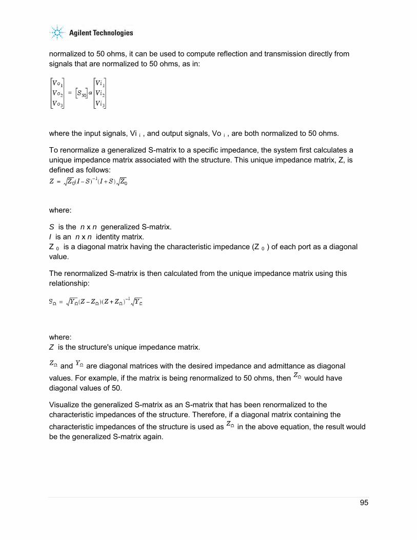
95
normalized to 50 ohms, it can be used to compute reflection and transmission directly from signals that are normalized to 50 ohms, as in:
where the input signals, Vi i , and output signals, Vo i , are both normalized to 50 ohms.
To renormalize a generalized S-matrix to a specific impedance, the system first calculates a unique impedance matrix associated with the structure. This unique impedance matrix, Z, is defined as follows:
where:
S is the n x n generalized S-matrix. I is an n x n identity matrix. Z 0 is a diagonal matrix having the characteristic impedance (Z 0 ) of each port as a diagonal value.
The renormalized S-matrix is then calculated from the unique impedance matrix using this relationship:
where: Z is the structure's unique impedance matrix.
and are diagonal matrices with the desired impedance and admittance as diagonal values. For example, if the matrix is being renormalized to 50 ohms, then would have diagonal values of 50.
Visualize the generalized S-matrix as an S-matrix that has been renormalized to the characteristic impedances of the structure. Therefore, if a diagonal matrix containing the characteristic impedances of the structure is used as in the above equation, the result would be the generalized S-matrix again.

Electromagnetic
96
Z- and Y-Matrices
Calculating and displaying the unique impedance and admittance matrices (Z and Y) associated with a structure is performed in the post processor.
Characteristic Impedances
FEM Simulator calculates the characteristic impedance of each port in order to compute a renormalized S-matrix, Z-matrix, or Y-matrix. The system computes the characteristic impedance of each port in three ways-as Z pi , Z pv , and Z vi impedances.
You have the option of specifying which impedance is to be used in the renormalization calculations.
PI Impedance The Z pi impedance is the impedance calculated from values of power (P) and current (I):
The power and current are computed directly from the simulated fields. The power passing through a port is equal to the following:
where the surface integral is over the surface of the port.
The current is computed by applying Ampere's Law to a path around the port:
While the net current computed in this way will be near zero, the current of interest is that flowing into the structure, I- or that flowing out of the structure, I+ . In integrating around the port, the system keeps a running total of the contributions to each and uses the average of the two in the computation of impedances.
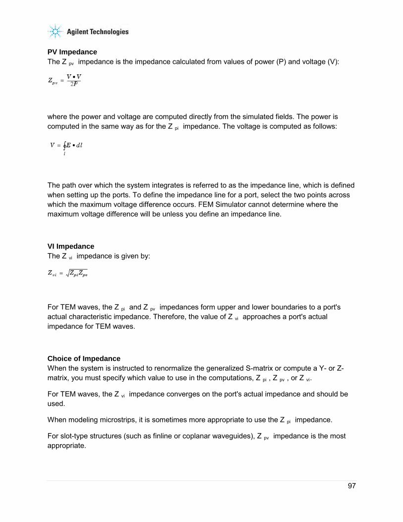
97
PV Impedance The Z pv impedance is the impedance calculated from values of power (P) and voltage (V):
where the power and voltage are computed directly from the simulated fields. The power is computed in the same way as for the Z pi impedance. The voltage is computed as follows:
The path over which the system integrates is referred to as the impedance line, which is defined when setting up the ports. To define the impedance line for a port, select the two points across which the maximum voltage difference occurs. FEM Simulator cannot determine where the maximum voltage difference will be unless you define an impedance line.
VI Impedance The Z vi impedance is given by:
For TEM waves, the Z pi and Z pv impedances form upper and lower boundaries to a port's actual characteristic impedance. Therefore, the value of Z vi approaches a port's actual impedance for TEM waves.
Choice of Impedance When the system is instructed to renormalize the generalized S-matrix or compute a Y- or Z-matrix, you must specify which value to use in the computations, Z pi , Z pv , or Z vi.
For TEM waves, the Z vi impedance converges on the port's actual impedance and should be used.
When modeling microstrips, it is sometimes more appropriate to use the Z pi impedance.
For slot-type structures (such as finline or coplanar waveguides), Z pv impedance is the most appropriate.

Electromagnetic
98
De-embedding
If a uniform length of transmission line is added to (or removed from) a port, the S-matrix of the modified structure can be calculated using the following relationship:
where:
is a diagonal matrix with the following entries:
γ = α + jβ is the complex propagation constant, where:
αi is the attenuation constant of the wave of port i. βi is the propagation constant associated with the uniform transmission line at port i. l i is the length of the uniform transmission line that has been added to or removed from the structure at port i. A positive value indicates that a length of transmission line has been removed from the structure.
The value of γ for the dominant mode of each port is automatically calculated by the 2D solver.
3.2.10 Equations
The sections below describe some of the equations that are solved in a simulation or used to define elements of a structure.
Derivation of Wave Equation
The solution to the following wave equation is found during a simulation:

99
where:
E( x,y,z ) is a phasor representing an oscillating electric field
k 0 is the free space wave number, . ω is the angular frequency, 2πf. µr( x,y,z ) is the complex relative permeability. εr( x,y,z ) is the complex relative permittivity.
The difference between the 2D and 3D solvers is that the 2D solver assumes that the electric field is a traveling wave with this form:
while the 3D solver assumes that the phasor E is a function of x, y, and z:
Maxwell's Equations
The field equation solved during a simulation is derived from Maxwell's Equations, which in their time-domain form are:
where:

Electromagnetic
100
E (t) is the electric field intensity.
D (t) is the electric flux density, ε E (t), and ε is the complex permittivity.
H (t) is the magnetic field intensity.
B (t) is the magnetic flux density, µ H (t), and µ is the complex permeability.
J (t) is the current density, σ E (t).
ρ is the charge density.
Phasor Notation Because all time-varying electromagnetic quantities are oscillating at the same frequency, they can be treated as phasors multiplied by ej ω t (in the 3D solver) or by ej ω t -γ z (in the 2D solver). In the general case with the 3D solver, the equations become:
By factoring out the quantity ej ω t and using the following relationships:

101
Maxwell's Equations in phasor form reduce to:
where B , H , E , and D are phasors in the frequency domain. Now, using the relationships B = µ H , D = ε E , and J = α E , Maxwell's Equations in phasor form become:
for σ = 0
where H and E are phasors in the frequency domain, µ is the complex permeability, and ε is the complex permittivity.
H and E are stored as phasors, which can be visualized as a magnitude and phase or as a complex quantity.

Electromagnetic
102
Electric and Magnetic Fields Can Be Represented as Phasors
Assumptions To generate the final field equation, place H in the equation in terms of E to obtain:
Then, substitute this expression for H in the equation to produce:
Conductivity
Although good conductors can be included in a model, the system does not solve for any fields inside these materials. Because fields penetrate lossy conductors only to one skin depth (which is a very small distance in good conductors), the behavior of a field can be represented with an equivalent impedance boundary.
For perfect conductors, the skin depth is zero and no fields exist inside the conductor. Perfect conductors are assumed to be surrounded with Perfect E boundaries.

103
Dielectric Loss Tangent
Dielectric losses can be modeled by assuming that the relative permittivity, , is complex:
Expressed in terms of the dielectric (electric) loss tangent, , the complex
relative permittivity, becomes:
Magnetic Loss Tangent
Losses in magnetic materials can be modeled by assuming that µr is complex.
Expressed in terms of the magnetic loss tangent, , the complex relative permeability becomes:
Definition of Freespace Phase Constant
Using the relationships and , the wave equation being solved can be placed in this form:
Electromagnetic
104
Now, if the free space phase constant (or wave number) is defined as, , the above reduces to the following equation that the 2D and 3D engines solve.:
3.3 Setting up FEM Simulations This section describes the process of creating and simulating a design with FEM.
3.3.1 Creating a Physical Design
You start with the physical dimensions of a planar design, such as a patch antenna or the traces on a multilayer printed circuit board. You can create a design in the following ways in ADS:
• Convert a schematic into a physical layout.
• Draw the design using Layout.
• Import a layout from another simulator or design system. Advanced Design System can import files in a variety of formats.
For information about converting schematics or drawing in Layout, see Schematic Capture and Layout documentation. For information on importing designs, see Importing and Exporting Designs.
3.3.2 Specifying Simulation Settings
In the EM Setup window, options required for specifying simulation settings are listed in the left pane. You can select the required option to open the settings in the right pane of the EM Setup window, as shown in the following figure:

105
You can specify settings for the following options:
• Layout: You can view information about the workspace, library, cell, and view by selecting Layout. For more information, refer Viewing Layout Information.
• Substrate: You can open a predefined substrate file from ADS by selecting Substrate. For more information, refer Defining Substrates in EM Simulations.
• Ports: You can refresh layout pins information, create, delete, and resequence ports, and search the required S-parameter ports or layout pins by selecting Ports. For more information, refer to Defining Ports in EM Simulations.
• Frequency Plan: You can add or remove frequency plans for your EM simulations by selecting Frequency Plan. For more information, see Defining a Frequency Plan.
• Output Plan: You can specify the data display settings for your EM simulations by selecting Output Plan. For more information, see Defining a Frequency Plan.
• Options: You can define the preprocessor, mesh, simulation, and expert settings by selecting Options. For more information, see Defining Simulation Options.

Electromagnetic
106
• Resources: You can specify the local, remote, and third party settings by selecting Resources. For more information, see Specifying Simulation Resources
• Model/Symbol: You can generate an EM model and symbol by selecting Model/Symbol. For more information, see Generating an EM Model and Symbol.
• Notes: You can add comments to your EM Setup window by selecting Notes.
3.3.3 Defining Substrates
A substrate is the media upon which the circuit resides. For example, a multilayer PC board consists of various layers of metal, insulating or dielectric material, and ground planes. Other designs may include covers, or they may be open and radiate into air. A complete substrate definition is required in order to simulate a design. The substrate definition includes the number of layers in the substrate and the composition of each layer. This is also where you position the layers of your physical design within the substrate, and specify the material characteristics of these layers.
For specifying a substrate for your FEM simulation, see Defining Substrates in an EM Simulation.
3.3.4 Assigning Port Properties
Ports enable you to inject energy into a circuit, which is necessary in order to analyze the behavior of your circuit. You apply ports to a circuit when you create the circuit, and then assign port properties in FEM Simulator. There are several different types of ports that you can use in your circuit, depending on your application.
For assigning ports in an FEM simulation, see Defining Ports in EM Simulations.
3.3.5 Defining the Frequency and Output Plan
You can set up multiple frequency plans for an FEM simulation. You can also specify the data display settings for your EM simulations by using the EM Setup Window.
For specifying a frequency and output plan, see Defining the Frequency and Output Plan.

107
3.3.6 Defining Simulation Options
You can specify global options, such as physical model, preprocessor, and mesh for FEM simulations. You can either use a predefined set of simulation options or or create a new set in Simulation Options of the EM Setup window. You can specify the following simulation options for an FEM simulation:
• Defining Preprocessor Settings
• Specifying Physical Model Settings for FEM
• Defining Solver Settings for FEM
• Defining Mesh Settings for FEM
3.3.7 Setting up Local, Remote, or Third Party Simulation
You can run FEM simulations on a local or remote machine, or take advantage of a third party load balancing and queuing system such as LSF, Sun Grid Engine, and PBS Professional.
For more information, see Specifying Simulation Resources.
3.3.8 Adding a Box or Waveguide
These elements enable you to specify boundaries on substrates along the horizontal plane. Without a box or waveguide, the substrate is treated as being infinitely long in the horizontal direction. This treatment is acceptable for many designs, but there may be instances where a boundaries need to be taken into account during the simulation process. A box specifies the boundaries as four perpendicular, vertical walls that make a box around the substrate. A waveguide specifies two vertical walls that cut two sides of the substrate.
For more information, see Adding Boxes, Waveguides, and Symmetry Planes.
3.3.9 Running FEM Simulations
You set up a simulation by specifying the parameters of a frequency plan, such as the frequency range of the simulation and the sweep type. When the setup is complete, you run the simulation. The simulation process uses the mesh pattern, and the electric fields in the design are calculated. S-parameters are then computed based on the electric fields. If the Adaptive

Electromagnetic
108
Frequency Sample sweep type is chosen, a fast, accurate simulation is generated, based on a rational fit model.
For more information, see Running FEM Simulations.
3.3.10 Viewing FEM Simulation Results
You can display the results of an FEM simulation by using the Data Display and Visualization window. You can display the various type of results from an FEM simulation such as S-parameters, radiation patterns (far-field plots) and derived antenna parameters.
For more information, see Visualizing 3D View before EM Simulation and Visualizing FEM Simulations.
3.3.11 Computing Radiation Patterns
Once the electric fields on the circuit are known, you can compute electromagnetic fields. The electric fields can be expressed in the spherical coordinate system attached to your circuit. For more information on radiation patterns, see Computing Radiation Patterns.
3.4 Example- Designing a Microstrip Filter This section describes the process of designing a microstrip coupled-line filter.
3.4.1 Drawing the Circuit
The circuit is drawn as a schematic, then converted to a layout. To start the process of designing a Microstrip filter, you need to draw the circuit by:
1. Creating a new workspace.
2. Adding Microstrip components to the schematic.
3. Converting the schematic to a layout.
Creating a New Workspace
To create a new workspace:
1. From the ADS Main window, choose File > New > Workspace to display New Workspace Wizard.
2. Click Next.

109
3. In the Workspace Name field, type step1.
4. Enter a path in Create In. Click Browse to select the location.
5. Click Next.
6. Under Add Libraries, select the libraries to be included in the Workspace, as shown in the following figure:
7. Click Next.
8. Under Library Name, enter a unique library name.
9. Click Next.
10. Under Technology, choose ADS Standard: length unit - mil.
11. Click Finish.
For more information about a workspace, refer Workspace.
Adding Components to the Schematic
The steps in this section describe how to select microstrip filter components.
1. In the Schematic window, click the Palette List arrow. The Palette List drops down.
2. Scroll and select T-lines Microstrip __ from the Palette List.
3. In the component palette, locate and click Mcfil. This selects the Libra Microstrip Coupled-Line Filter Section component.
4. Crosshairs and a ghost icon of the component appear as you move the cursor over the Schematic window. Position the cursor and click.
5. End the command either by clicking the Cancel Command button or by choosing Insert or the arrow button.
3.4.2 Editing the Component
This section describes how to edit several component parameters, such as the length and width, and also how to change the parameters that are displayed below the component.
1. To edit the component parameters, double click the component.
2. Select a parameter and set the values for these parameters:

Electromagnetic
110
o W = line width = 0.25 mm
o S = spacing between lines = 0.044 mm
o L = line length = 1.8 mm
o W1 = width of the line that connects to pin 1 = 0.25 mm
o W2 = width of the line that connects to pin 2 = 0.25 mm
3. Click OK to accept the edits and dismiss the dialog box.
3.4.3 Copying and Placing another Component
This section describes how to make a copy of the filter section and add it to the schematic.
1. Click the filter component on the schematic to select it. A black outline appears around it.
2. From the Schematic window, choose Edit > Copy.
3. Choose Edit > Paste. ** Move the crosshairs so that they are directly over the left connector of the first component and click.
4. End the current command.
3.4.4 Adding Ports
Ports are required on a circuit. If you forget to add ports to the schematic, you can always add them later after the schematic is converted to a layout. In this exercise, ports will be added to the layout.
With FEM, you can define additional characteristics to a port.
3.4.5 Generating the Layout
This section describes how to covert the microstrip coupled-line filter schematic that you just finished to a layout.
1. From the Schematic window, choose Layout > Generate/Update Layout. The Generate/Update Layout dialog box and a Layout window appear.

111
2. From the Layout window, choose Options > Preferences. Click the Layout Units __ tab and set the Resolution to 0.001 mm. Click OK.
3. In the Generate/Update Layout dialog box, enter -1.8 in the X field and 0.294 in the Y field. This step identifies the placement of P1 on the layout. This step is usually optional, but specifying the location will be helpful later when the box is added to enclose the filter. Click OK.
4. A window displaying the results of the conversion is displayed. Click OK. A layout representation of the schematic appears in the Layout window. It should resemble the figure here.
5. From the layout window, choose File > Save. The layout name is filter. You now have a layout and a schematic as part of your project.
3.4.6 Defining a Substrate
This circuit uses a relatively simple substrate. In this exercise, the thickness of some of the layers is modified. A more important task is that ground planes are added to the top and bottom of the substrate. These ground planes form the top and bottom of the metal box in which the filter will be enclosed. The substrate will have the following layers:
• A ground plane representing the top of the box
• A layer of air
• The microstrip filter traces
• A layer of Alumina
• A ground plane representing the bottom of the box.
1. Select EM > Simulation Setup to open the EM Setup window.
2. Select Substrate in the left pane of the EM Setup window.
3. Click New to create a substrate.

Electromagnetic
112
4. Specify the library and view name and select a template.
5. Click OK.
6. Select the top layer in the Substrate Layers field. Specify the bounding area layer. The top ground plane is added to the substrate.
7. In the Substrate Layers list, select Free_Space. Change the Thickness to 2846 um. This sets the layer of air to an appropriate thickness.
8. In the Substrate Layers list, select Alumina. Change the Thickness to 254 um.
9. Keep the bottom ground plane, but select and Cut any other layers that may appear in the substrate.
10.
Note The top and bottom of the box enclosure are defined with groundplanes, the sides of the enclosure will be defined later in this exercise.
You currently see four of the five substrate layers that you need. In this instance, the metal layer is automatically positioned between the Alumina and air layers. Note the following points about this layer:
o Metal layers are identified by a dashed line.
o The word cond identifies the layout layer that is mapped to this position. Refer to the Layout window, and you will see that the microstrip circuit was automatically applied to the layout layer named cond during the translation process.
o The word strip defines the layer such that the microstrips are metal and what surrounds the microstrips on that layer is air or dielectric. Other choices are slot and via. These are described in the exercise in the next section.
11. Choose File > Save As. Specify the file name as filter and click Save. The substrate file filter.slm is saved as part of the project.
3.4.7 Adding Ports to the Layout
In FEM, you can define the ports in your circuit to be one of several types. Depending on the type you choose, the ports will be characterized in different ways. This can impact the result of a simulation, because the simulation can take these characteristics into account. With different port types, you can select one that best matches the intended application of your layout.
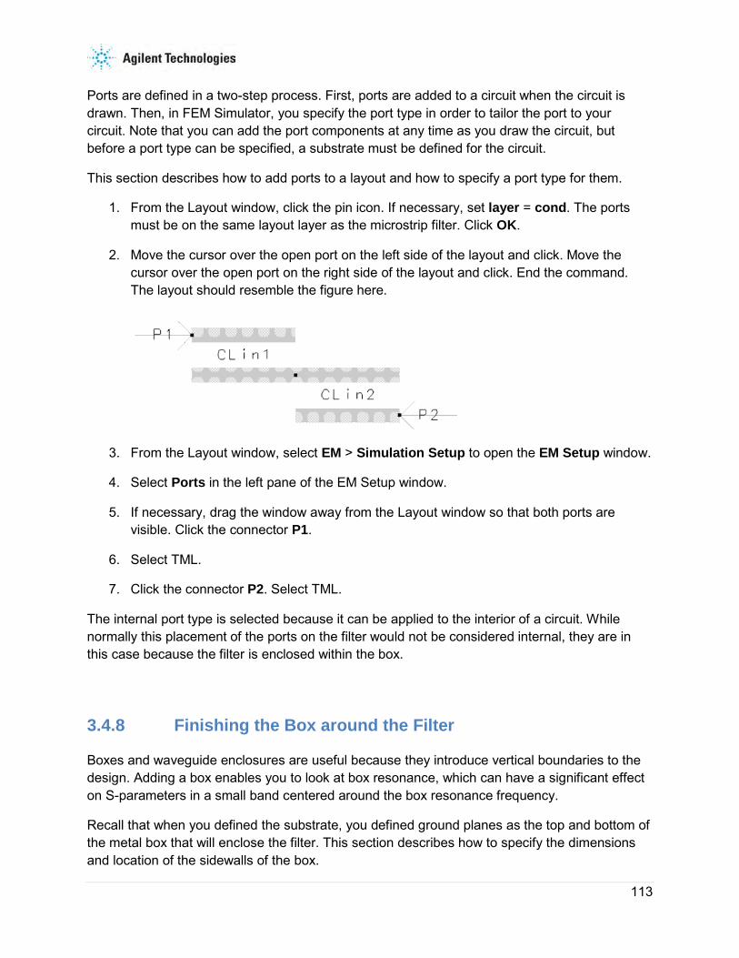
113
Ports are defined in a two-step process. First, ports are added to a circuit when the circuit is drawn. Then, in FEM Simulator, you specify the port type in order to tailor the port to your circuit. Note that you can add the port components at any time as you draw the circuit, but before a port type can be specified, a substrate must be defined for the circuit.
This section describes how to add ports to a layout and how to specify a port type for them.
1. From the Layout window, click the pin icon. If necessary, set layer = cond. The ports must be on the same layout layer as the microstrip filter. Click OK.
2. Move the cursor over the open port on the left side of the layout and click. Move the cursor over the open port on the right side of the layout and click. End the command. The layout should resemble the figure here.
3. From the Layout window, select EM > Simulation Setup to open the EM Setup window.
4. Select Ports in the left pane of the EM Setup window.
5. If necessary, drag the window away from the Layout window so that both ports are visible. Click the connector P1.
6. Select TML.
7. Click the connector P2. Select TML.
The internal port type is selected because it can be applied to the interior of a circuit. While normally this placement of the ports on the filter would not be considered internal, they are in this case because the filter is enclosed within the box.
3.4.8 Finishing the Box around the Filter
Boxes and waveguide enclosures are useful because they introduce vertical boundaries to the design. Adding a box enables you to look at box resonance, which can have a significant effect on S-parameters in a small band centered around the box resonance frequency.
Recall that when you defined the substrate, you defined ground planes as the top and bottom of the metal box that will enclose the filter. This section describes how to specify the dimensions and location of the sidewalls of the box.

Electromagnetic
114
1. From the Layout window, choose EM > Box & Waveguide > Add Box.
2. Type x, y coordinates for the left and right sides of the box. Choose Insert > Coordinate Entry. Type -4.5 , -4.5 in the X,Y fields of the Coordinate Entry dialog box and click Apply.
3. Type +4.5 , +4.5 in the X,Y fields of the Coordinate Entry dialog box and click Apply. The box appears as shown below (you may need to click View All to see the box). Click Cancel to close the dialog box.
3.4.9 Performing the Simulation
This section describes how to set up and run the simulation. In this exercise, the adaptive sweep type is used in the simulation process. This the preferred sweep type, because it used a fast, highly accurate method of comparing simulated data points to a rational fitting model. Unlike the linear sweep type, where simulated data points are chosen in a linear fashion based on step size, adaptive sweep type data points are chosen based on where the most variance seen. Wherever S-parameters vary from the rational fitting model the most, more samples are taken.
1. From the Layout window, choose EM > Simulation Setup.
2. Select FEM.
3. Select Frequency Plan in the left pane of the EM Setup window.
4. Select the Adaptive Sweep Type and set these parameters to the following values:
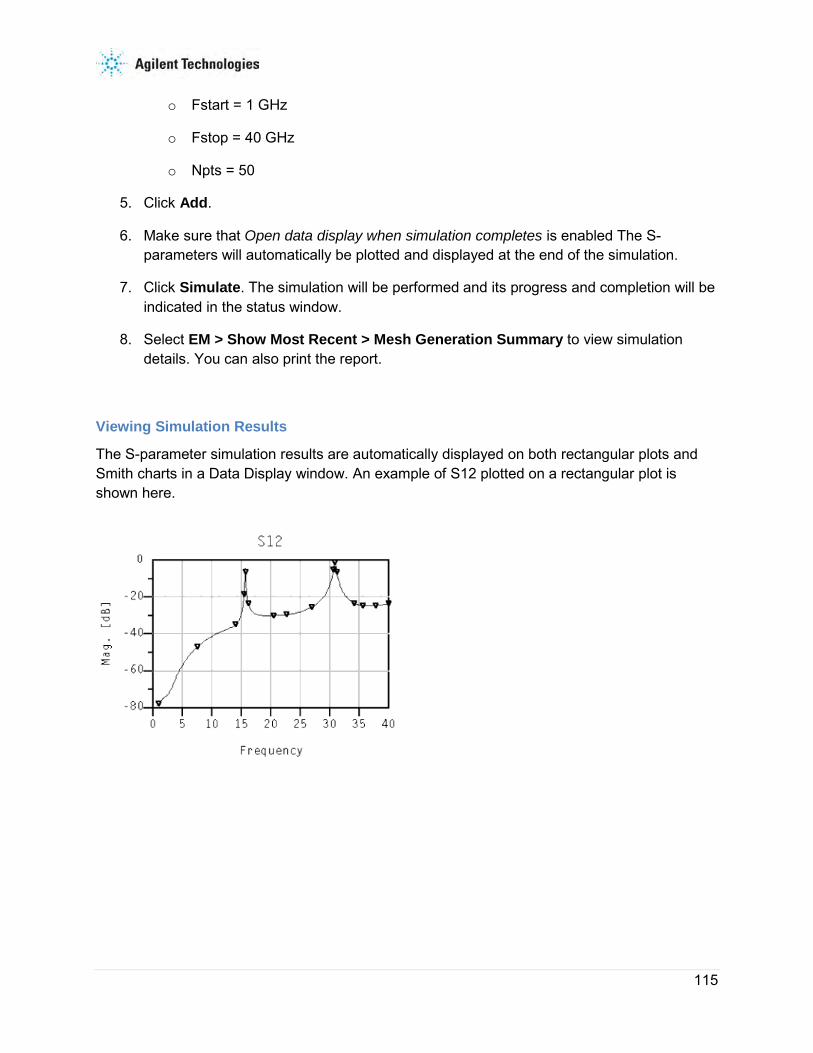
115
o Fstart = 1 GHz
o Fstop = 40 GHz
o Npts = 50
5. Click Add.
6. Make sure that Open data display when simulation completes is enabled The S-parameters will automatically be plotted and displayed at the end of the simulation.
7. Click Simulate. The simulation will be performed and its progress and completion will be indicated in the status window.
8. Select EM > Show Most Recent > Mesh Generation Summary to view simulation details. You can also print the report.
Viewing Simulation Results
The S-parameter simulation results are automatically displayed on both rectangular plots and Smith charts in a Data Display window. An example of S12 plotted on a rectangular plot is shown here.
Electromagnetic
116
Chapter 4 – Setting up EM Simulations
ADS simplifies the overall process of setting up EM simulations. The new EM usability provides a user-friendly EM Setup window for defining Momentum and FEM simulations. Using the EM Setup window, you can specify the settings for your EM simulation from a single interface. You can assign substrates, configure ports, define frequency and output plans, specify local, remote or distributed setup options, and customize the EM data name generated during a simulation.
This section provides the following information about setting up EM simulations:
• Overview
• Viewing Layout Information
• Substrates
o Defining Substrates in EM Simulations
o Substrates in EM Simulation
o Sweeping Substrate Name and Mesh Density
o Adding Boxes, Waveguides, and Symmetry Planes
• Ports
o Defining Ports in EM Simulations
o Setting up Ports
o Using Ports in Momentum
o Using Ports in FEM
• Defining a Frequency Plan
• Defining an Output Plan
• Defining Simulation Options
o Specifying Physical Model Settings for Momentum
o Specifying Physical Model Settings for FEM
o Defining Preprocessor Settings
117
o Defining Mesh Settings for Momentum
o Defining Mesh Settings for FEM
o Defining Solver Settings
• Specifying Simulation Resources
• Using the Job Manager
• Generating an EM Model and Symbol
• Using an EM Setup Template
4.1 Overview ADS provides an improved EM Simulation usability. It is now easier to create and use EM models for arbitrary parts of a layout by designers who are not EM experts. ADS provides a new EM GUI, EM Setup window, which provides a single interface to control all EM setup related features. It provides a:
• Unified EM interface to reduce maintenance efforts.
• User-friendly interface for defining Momentum and FEM simulations.
4.1.1 Using the EM Setup Window
To open the EM Setup window, choose EM > Simulation Setup. The EM Setup window enables you to define simulator options such as substrate, ports, and frequency plan. The following figure displays an EM Setup window:

Electromagnetic
118
The following sections describe the EM Setup window:
• EM Setup Options
• EM Simulators
• EM Setup Summary
• EM Setup Window Menu Options
• EM Toolbar Options
EM Setup Options
In the EM Setup window, options required for specifying simulation settings are listed in the left pane. You can select the required option to open the settings in the right pane of the EM Setup window, as shown in the following figure:
119
• Layout: You can view information about the workspace, library, cell, and view by selecting Layout. For more information, refer Viewing Layout Information.
• Substrate: You can open a predefined substrate file from ADS by selecting Substrate. For more information, refer Defining Substrates in EM Simulations.
• Ports: You can refresh layout pins information, create, delete, and resequence ports, and search the required S-parameter ports or layout pins by selecting Ports. For more information, refer to Defining Ports in EM Simulations.
• Frequency Plan: You can add or remove frequency plans for your EM simulations by selecting Frequency Plan. For more information, see Defining a Frequency Plan.
• Output Plan: You can specify the data display settings for your EM simulations by selecting Output Plan. For more information, see Defining a Frequency Plan.
• Options: You can define the preprocessor, mesh, simulation, and expert settings by selecting Options. For more information, see Defining Simulation Options.
• Resources: You can specify the local, remote, and third party settings by selecting Resources. For more information, see Specifying Simulation Resources
• Model/Symbol: You can generate an EM model and symbol by selecting Model/Symbol. For more information, see Generating an EM Model and Symbol.
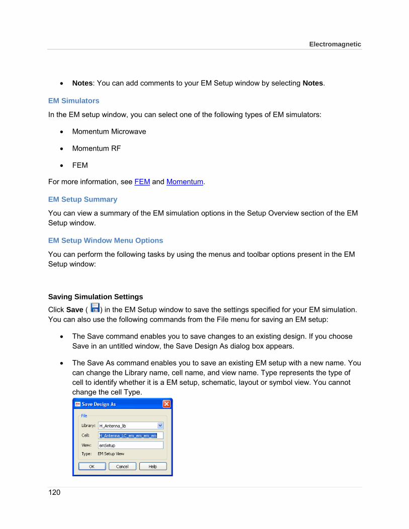
Electromagnetic
120
• Notes: You can add comments to your EM Setup window by selecting Notes.
EM Simulators
In the EM setup window, you can select one of the following types of EM simulators:
• Momentum Microwave
• Momentum RF
• FEM
For more information, see FEM and Momentum.
EM Setup Summary
You can view a summary of the EM simulation options in the Setup Overview section of the EM Setup window.
EM Setup Window Menu Options
You can perform the following tasks by using the menus and toolbar options present in the EM Setup window:
Saving Simulation Settings
Click Save ( ) in the EM Setup window to save the settings specified for your EM simulation. You can also use the following commands from the File menu for saving an EM setup:
• The Save command enables you to save changes to an existing design. If you choose Save in an untitled window, the Save Design As dialog box appears.
• The Save As command enables you to save an existing EM setup with a new name. You can change the Library name, cell name, and view name. Type represents the type of cell to identify whether it is a EM setup, schematic, layout or symbol view. You cannot change the cell Type.
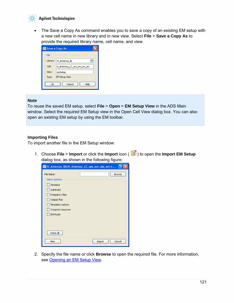
121
• The Save a Copy As command enables you to save a copy of an existing EM setup with a new cell name in new library and in new view. Select File > Save a Copy As to provide the required library name, cell name, and view.
Note To reuse the saved EM setup, select File > Open > EM Setup View in the ADS Main window. Select the required EM Setup view in the Open Cell View dialog box. You can also open an existing EM setup by using the EM toolbar.
Importing Files To import another file in the EM Setup window:
1. Choose File > Import or click the Import icon ( ) to open the Import EM Setup dialog box, as shown in the following figure:
2. Specify the file name or click Browse to open the required file. For more information, see Opening an EM Setup View.

Electromagnetic
122
3. Select the required sections from the Select sections list. You can also select all the sections by clicking Check all.
4. Click Import.
Opening an EM Setup View To open an EM setup view, perform the following the steps:
1. Start ADS and open an existing workspace.
2. From the ADS Main window, choose File > Open > EM Setup View to open the Specify EM Cell View dialog box.
3. Select EM Setup View from the Type drop-down list.
4. If you want to open a built-in ADS design (read-only), check the Show ADS Libraries checkbox to display the list of all libraries under Library.
5. Under Library, select the Library name where the view exists.
6. Under Cell, select the cell name.
7. Under View, select the required EM setup view name.
8. Click OK to open the selected EM setup view.
Opening the 3D Preview window
Choose Tools > 3D EM Preview or click the 3D EM Preview icon ( ) to preview your simulation.
123
Opening the Layout window
Choose Tools > Open Layout Window or click the Open Layout Window icon ( ) to display a layout window.
Simulating a Design You can save the current settings and start the simulation process by clicking the Simulate
button or click ( ) to simulate an EM simulation. You can also press F7 to start the EM simulation. If you have specified invalid EM settings, an error message is displayed.
4.1.2 EM Toolbar Options
You can also use the EM toolbar to perform EM simulations. The EM toolbar provides shortcuts to the frequently-used menus. It is present in the Layout window. You can perform the following tasks by using EM toolbar options:
• Starting an EM simulation: Click Start EM Simulation ( ) to initiate the simulation process.
• Stopping an EM simulation: Click Stop EM Simulation ( ) to stop an EM simulation and release the license.
• Opening the EM Setup window: Click EM Simulation Setup ( ) to display the EM Setup window.
• Opening the substrate editor window: Click Substrate Editor ( ) to open the substrate editor window.
• Opening the 3D Preview window: Click 3D EM Preview ( ) to preview an EM simulation.
• Opening the 3D Viewer window: Click Visualization ( ) to open the 3D Viewer and load the simulation results of the current EM setup.
Electromagnetic
124
• Calculating far fields: Click Far Field ( ) to calculate far fields from the simulation results of the current EM setup.
4.2 Viewing Layout Information You can view information about the current layout in the EM Setup window. This window provides the following information about the location of a workspace, library, cell, and view of the current layout:
• Workspace: Specifies the complete path to the location where you have saved the workspace file.
• Library: Specifies the name of the library.
• Cell: Specifies the name of the cell.
• View: Specifies the view that is opened for setting up the EM simulation.
Note For more information about a workspace, library, cell, and view, see New Terminologies.
From the EM Setup window, you can also open the structure in the following window:
• 3D view
• Layout window
4.2.1 Displaying Layout Information
To display the layout information for your EM simulation:
1. Select EM > Simulation Setup to open the EM Setup window.
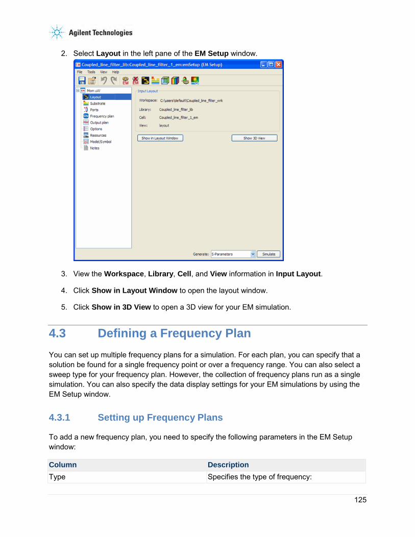
125
2. Select Layout in the left pane of the EM Setup window.
3. View the Workspace, Library, Cell, and View information in Input Layout.
4. Click Show in Layout Window to open the layout window.
5. Click Show in 3D View to open a 3D view for your EM simulation.
4.3 Defining a Frequency Plan You can set up multiple frequency plans for a simulation. For each plan, you can specify that a solution be found for a single frequency point or over a frequency range. You can also select a sweep type for your frequency plan. However, the collection of frequency plans run as a single simulation. You can also specify the data display settings for your EM simulations by using the EM Setup window.
4.3.1 Setting up Frequency Plans
To add a new frequency plan, you need to specify the following parameters in the EM Setup window:
Column Description Type Specifies the type of frequency:
Electromagnetic
126
Column Description • Adaptive: It is the preferred sweep
type. It uses a fast and accurate method of comparing sampled S-parameter data points to a rational fitting model. The value entered in the Sample Points Limit field is the maximum number of samples used in an attempt to achieve convergence. The solutions from the final attempt will be saved. If convergence is achieved using fewer samples, the solutions are saved and the simulation will end.
• Linear: It simulates over a frequency range, selecting the frequency points to be simulated in linear increments based on the step size you specify. Type the start and the stop frequencies in the Start and Stop fields, and select frequency units for each. Enter the step size in the Step field, and select units.
• Log:It simulates over a frequency range, selecting the frequency points to be simulated in logarithmic increments. Type the start and the stop frequencies in the Start and Stop fields, and select frequency units for each. Enter the number of frequency points to be simulated per decade of frequency in the Points/Decade field, and select units.
• Single: It simulates at a single frequency point. Type the value in the Frequency field and select the units.
Fstart Specifies the frequency start value. Set a unit,
such as Hz, KHz, MHz, GHz, or THz, for the selected value.
Fstop Specifies the frequency stop value. Set a unit, such as Hz, KHz, MHz, GHz, or THz, for the selected value.

127
Column Description Npts Specifies the number of frequencies to
simulate. For Adaptive this is the maximun number of samples to use.
Step Specifies the step value. Set a unit, such as Hz, KHz, MHz, GHz, or THz, for the selected value.
Enabled Allows you to enable the frequency plan.
Adding a Frequency Plan
To add a frequency plan:
1. Choose EM> Simulation Setup to display the EM Setup window.
2. Select Frequency Plan in the left pane of the EM Setup window.
3. To add a new frequency plan, click Add.
4. Select a sweep from the Type column.

Electromagnetic
128
5. Specify the frequency start value in the Fstart column.
6. Specify the frequency stop value in the Fstop column.
7. Specify the value of N points in the Npts column.
8. Specify the step value in the Step column.
9. Select the check box in the Enabled column to enable the frequency plan.
10. Repeat the preceding steps to insert additional frequency plans.
Note In a simulation, the frequency plans are executed in the order they appear in this list with the exception that the Adaptive sweep only starts if all others have been executed
Removing a Frequency Plan
To delete a frequency plan:
1. Choose EM> Simulation Setup.
2. Select Frequency Plan in the EM Setup window.
3. Select the required frequency plan.
4. Click Remove.
4.4 Defining an Output Plan You can set up multiple frequency plans for a simulation. For each plan, you can specify that a solution be found for a single frequency point or over a frequency range. You can also select a sweep type for your frequency plan. However, the collection of frequency plans run as a single simulation. You can also specify the data display settings for your EM simulations by using the EM Setup Window.
You can specify a dataset for storing results by using the EM Setup window. You can perform the tasks described in this section.

129
4.4.1 Selecting an Output Dataset
When you run an EM simulation, the results are stored in a dataset. This dataset is then used by Data Display for viewing results. You can select the name and location of the dataset you want to use for a simulation. The default value is the cell name. Datasets are stored in a workspace or data subdirectory. You can also select a dataset name from the existing dataset file names. When using an existing name, new results overwrite existing contents. This means that you should provide unique names for the datasets that will be generated from different cells in the same workspace directory.
Specifying a Dataset
To select an output dataset:
1. Select EM > Simulation Setup to display the EM Setup window.
2. Select Output Plan in the left pane of the EM Setup window.
3. Click Edit. The Choose Output Names dialog box is displayed.
You can also select EM > Choose Output Names to open the Choose Output Names dialog box.
4. Type a name for the dataset where you want simulation data to be saved.
5. You can also click Browse to view the existing dataset names in the current workspace, as shown in the following figure:
6. Select the required dataset and click OK.
7. The Append text specified in simulation setup check box is selected by default.
8. Click OK.
4.4.2 Customizing the Dataset Naming Convention
You can customize the naming convention of the dataset generated during a simulation by adding a prefix or suffix to the data name. To generate the dataset with the required naming

Electromagnetic
130
convention, you can select Appending text to the dataset name. You can select one of the following options for customizing the data name in Append text to the name:
• View name: Select the View name option in the From the layout view section to add text from the layout view.
• Adding simulation type: Select Simulation type include the type of simulator in the dataset name by selecting Simulation Type.
• Adding simulation options: Select Simulation options in the From the simulation setup view section to add text from the simulation setup view.
• Adding user-defined text: You can add a suffix to the dataset name in the This text field.
4.4.3 Specifying Data Display Settings
You can select options to open data display after completing the simulation process.
Open data display when simulation completes: Automatically opens the data display window on the completion of a simulation.
You can also insert a template in a new or empty data display by using one of the following options:
• Auto-select based on number of ports: Selects a template automatically based on the number of ports.
• User-defined file: Enables you to specify a template. You can also perform the following steps to select the required template:
1. Click Browse to open the Data Display Insert Template window, as shown in the following figure:
131
2. By default, the Momentum Product option is selected in the left pane of the Data Display Insert Template window.
3. Select the required template.
4. Click OK.
4.4.4 Reusing Simulation Data
To reduce the time required to complete the current simulation, you can use sampled data from the previous simulation. This function is useful if you extend or shift the frequency plan and re-simulate, or if you want more samples near a resonance frequency. If you change the circuit geometry, substrate, ports, or mesh parameters, simulation data cannot be reused. Enabling the function reuses previously calculated S-50 parameters.
ADS does not verify that the design has not changed. Make sure that only the frequency plan has changed before attempting to reuse data.
To reuse data from the last simulation:
1. Select EM > Simulation Setup to display the EM Setup window.
2. Select Output Plan in the left pane of the EM Setup window.
3. Enable Reuse files from the previous simulation if you want to use data from the previous simulation. Sampled data from the previous simulation will be used in the
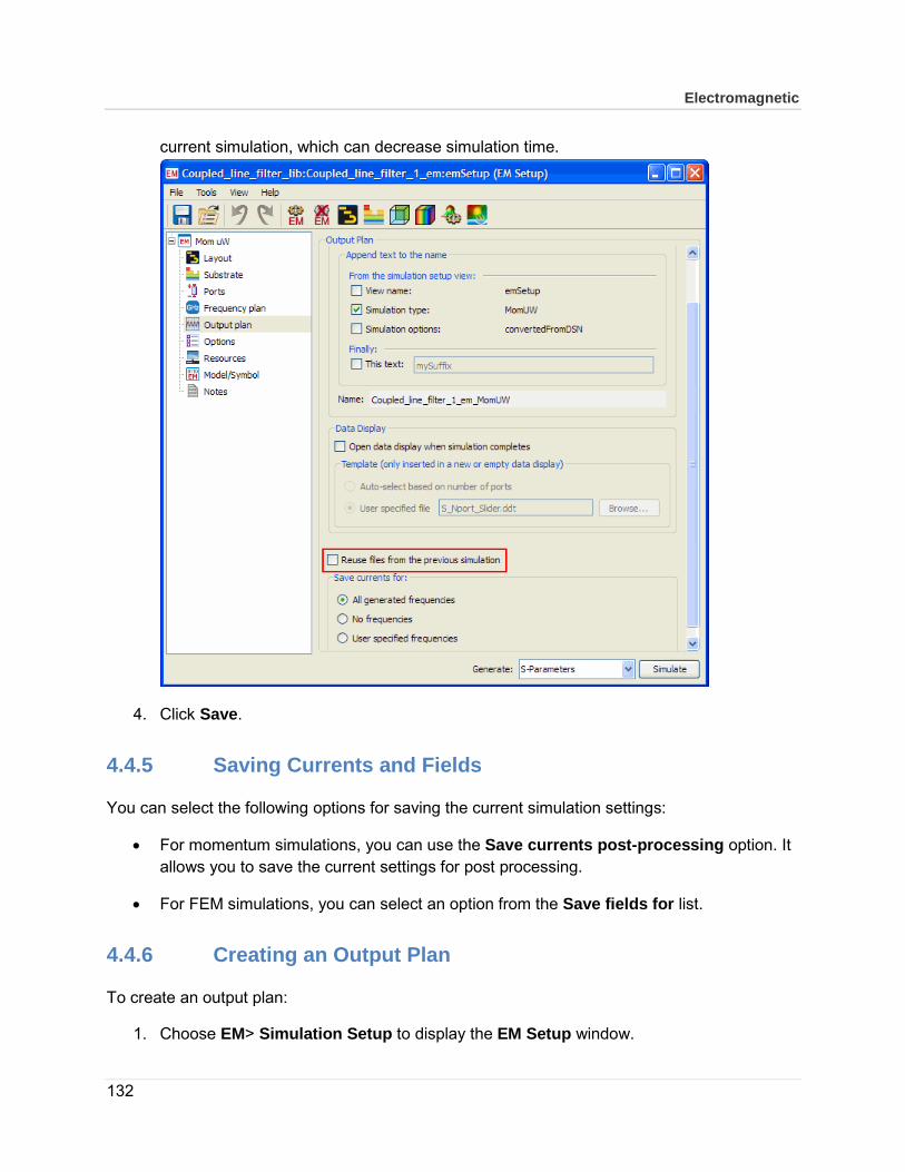
Electromagnetic
132
current simulation, which can decrease simulation time.
4. Click Save.
4.4.5 Saving Currents and Fields
You can select the following options for saving the current simulation settings:
• For momentum simulations, you can use the Save currents post-processing option. It allows you to save the current settings for post processing.
• For FEM simulations, you can select an option from the Save fields for list.
4.4.6 Creating an Output Plan
To create an output plan:
1. Choose EM> Simulation Setup to display the EM Setup window.

133
2. Select Output Plan in the left pane of the EM Setup window.
3. The default dataset name is displayed. To specify a new dataset, click Edit. For more information, see Selecting an Output Dataset.
4. Select an option for appending text to the dataset name.
5. Select Open data display when simulation completes, if you want to open the data display window automatically.
6. Specify the template to be used for displaying the data in Template. You can also click Browse to select the required template.
7. Select Reuse files from previous simulation if you want to use the previous simulation files.
8. Select Save currents for post-processing.
4.5 Defining Simulation Options You can specify engine-specific options, such as physical model, preprocessor, and mesh for EM simulations. You can either use a predefined set of simulation options or or create a new set in Simulation Options of the EM Setup window. You can perform the following operations to edit the list of simulation sets:
• Creating a copy of the option set: You can create a copy of the predefined simulation set by clicking Copy as. Specify a name for the copied option. You can now define new simulation options in this set.
• Renaming an option set: You can change the name of your simulation set by clicking Rename.
• Removing an option set: You can delete a simulation set by clicking Remove. After you remove a simulation set, the simulation set value changes to Default in the drop-down list.
To create a new set of simulation options:
1. Choose EM > Simulation Setup to open the EM Setup window.
2. Select Options in the left pane of the EM Setup window, as shown in the following figure:

Electromagnetic
134
3. Click Create a copy.
4. Specify a name for the copied option.
5. Define new simulation options in the EM Setup window.
4.5.1 Specifying Simulation Options
You can specify preprocessor, mesh, and simulation settings by using the Simulation Options dialog box. It consists of the following tabs:
• Description
• Substrate
• Preprocessor
• Mesh

135
• Simulation
• Expert
In the Description tab, you can add information about the simulation options. The following sections provide information about the other tabs available in the EM Setup window:
• Specifying Physical Model Settings for Momentum
• Specifying Physical Model Settings for FEM
• Defining Preprocessor Settings
• Defining Mesh Settings for Momentum
• Defining Mesh Settings for FEM
• Defining Solver Settings
4.5.2 Specifying Physical Model Settings for Momentum
You can specify the physical model parameters such as model type and lumped and wire via options in a Momentum simulation. You can specify these parameters either globally or on selected layers.
Specifying Global Modeling Options
Using the Global tab, you can specify the modeling type for thick conductors and vias. To identify the conductive areas of a layout layer, you can define the model type for current. The current flow at the surface is modeled depending on the simulation model chosen. You can choose the following modeling options:
• Lumped Model
• 2D Distributed Model
• 3D Distributed
The 2D Distributed Model is the default via simulation model. The Lumped Model can be used to more efficiently simulate contact via's (the main purpose of which is to provide electrical or mechanical contact). The 3D Distributed Model yields a full 3D modeling of all the components of the via currents (including the horizontal via currents) and can be used to more accurately simulate the electrical behavior of a signal via.
Lumped Model • A lumped element network represents the via connection. The actual via mesh is
ignored and a single lumped branch, connecting the largest bottom and top cell covering the via object (or touching in case of an open polyline via), models the via connection.

Electromagnetic
136
• Each via object contributes only one extra unknown to the matrix equation, the lumped via current, which has only a vertical component with a constant amplitude.
• A lumped series R, L impedance is used as electrical model in the simulation of the via.
• The resistance R and inductance L of the via are automatically calculated from the geometry and the material parameters.
• The mutual inductances are NOT included.
• The self and mutual capacitances are NOT included.
• The via cells do NOT contribute to the matrix equation load process.
The internal impedance (resistance and internal inductance) of the via follows from the application of the surface impedance concept for a uniform vertical current distribution on the via. That is, we have:
For via mask layers specified by a conductivity, the surface impedance Zs includes the skin effect. Hence, the frequency dependent skin effects (yielding a higher resistance and a lower internal inductance as frequency increases) are included in the lumped via model. For via mask layers specified by an impedance, the frequency dependent skin effect is NOT included.
2D Distributed Model You can specify this value for both thick conductor and vias simulation models. For a 2D distributed value,a distributed model for an object is created based on the surface mesh. At the vertical side walls, the vertical component of the current is modeled only, using vertical oriented rooftop functions. Hence, the modeled current distribution of the vertical component varies both in the cross-section and in the vertical direction (2D current distribution).
• A distributed model for the via object is created based on its surface mesh.

137
• At the vertical side walls, the vertical component of the via current is modeled only, using vertical oriented rooftop functions. Hence, the modeled current distribution of the vertical component varies both in the cross-section and in the vertical direction (2D current distribution).
• Each via object contributes two unknown currents per rectangular side wall cell to the matrix equation
• The via resistance is modeled as part of the surface impedance, similar to how strip metallizations are treated. The skin effect will be included if the via material is specified by a conductivity.
• The via self and mutual inductances (vertical currents only) and capacitances are included in the simulation.
3D Distributed Model You can specify this value for both thick conductor and vias simulation models. For a 3D distributed value, a distributed model for an object is created based on its surface mesh. At the vertical side walls, both the horizontal and vertical components of the current are modeled, using horizontal and vertical oriented rooftop functions. This yields a complete 3D current modeling of the objects.
• A distributed model for the via object is created based on its surface mesh.
• At the vertical side walls, both the horizontal and vertical components of the via current are modeled, using horizontal and vertical oriented rooftop functions. This yields a complete 3D current modeling of the via objects.
• Each via object contributes four unknown currents per rectangular side wall cell to the matrix equation.
• The via resistance is modeled as part of the surface impedance, similar to how strip metallizations are treated. The skin effect will be included if the via material is specified by a conductivity.
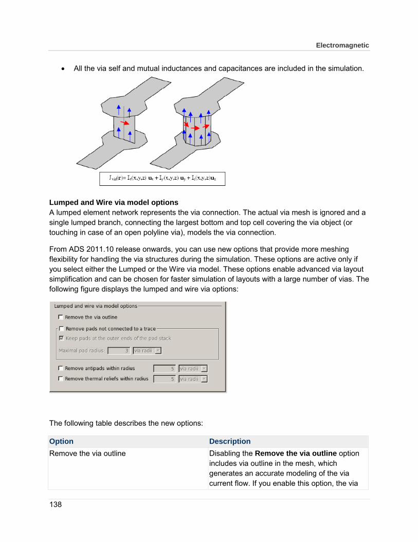
Electromagnetic
138
• All the via self and mutual inductances and capacitances are included in the simulation.
Lumped and Wire via model options A lumped element network represents the via connection. The actual via mesh is ignored and a single lumped branch, connecting the largest bottom and top cell covering the via object (or touching in case of an open polyline via), models the via connection.
From ADS 2011.10 release onwards, you can use new options that provide more meshing flexibility for handling the via structures during the simulation. These options are active only if you select either the Lumped or the Wire via model. These options enable advanced via layout simplification and can be chosen for faster simulation of layouts with a large number of vias. The following figure displays the lumped and wire via options:
The following table describes the new options:
Option Description Remove the via outline Disabling the Remove the via outline option
includes via outline in the mesh, which generates an accurate modeling of the via current flow. If you enable this option, the via

139
Option Description outline is ignored during meshing, which results in a mesh with fewer cells around the via connections.
Remove pads not connected to a trace Disabling the Remove pads not connected to a trace option includes the via pads in the mesh, which generates an accurate modeling of the via current flow. If you enable Remove pads not connected to a trace, the via pads (not connected to a trace) are ignored during meshing, which results in a mesh with fewer cells.
Remove antipads within radius Disabling the Remove antipads within radius option includes the via antipads (clearances in the ground plane) in the mesh, which generates accurate modeling of the ground plane current flow. If you enable Remove antipads within radius, the via antipads within a radius smaller than the specified number of via radii is ignored during meshing, which results in a mesh with fewer cells.
Remove thermal reliefs within radius Disabling the Remove thermal reliefs within radius option includes the via thermal reliefs in the mesh, which generates accurate modeling of the via current flow. If you enable Remove thermal reliefs within radius, the via thermal reliefs within a radius smaller than the specified number of via radii is ignored during meshing, which results in a mesh with fewer cells.
If you convert a project from an older ADS version, the wire vias options are disabled, by default. Therefore, results are same in the original project and the converted workspace.
Guidelines for Lumped and Wire Via Models The lumped and wire via models are subject to the following restrictions:
• Vias that are strictly partially connecting to a pad, trace, or plane cannot be simulated using a lumped or wire model. You can use the 3D Distributed model for simulation.
• Via shapes where center is outside the shape uses the 3D Distributed model for simulation.
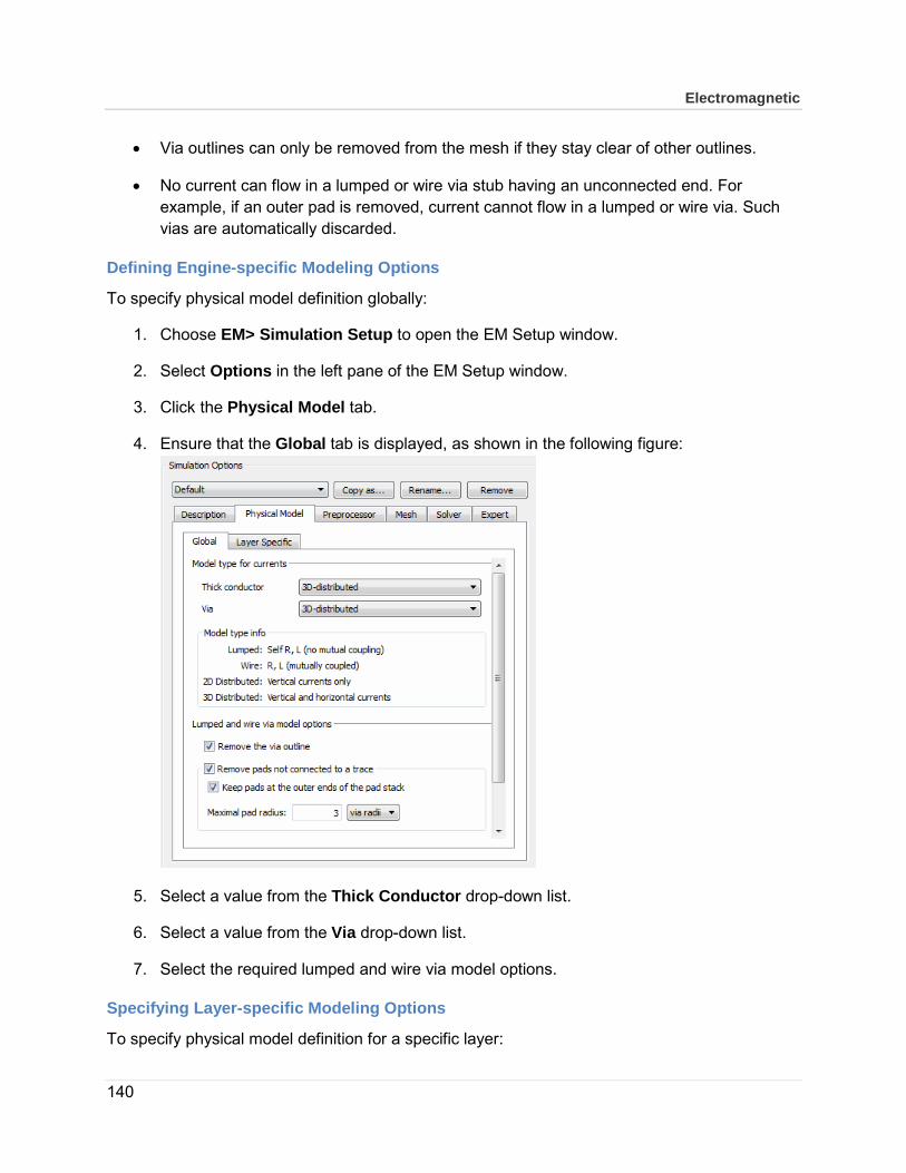
Electromagnetic
140
• Via outlines can only be removed from the mesh if they stay clear of other outlines.
• No current can flow in a lumped or wire via stub having an unconnected end. For example, if an outer pad is removed, current cannot flow in a lumped or wire via. Such vias are automatically discarded.
Defining Engine-specific Modeling Options
To specify physical model definition globally:
1. Choose EM> Simulation Setup to open the EM Setup window.
2. Select Options in the left pane of the EM Setup window.
3. Click the Physical Model tab.
4. Ensure that the Global tab is displayed, as shown in the following figure:
5. Select a value from the Thick Conductor drop-down list.
6. Select a value from the Via drop-down list.
7. Select the required lumped and wire via model options.
Specifying Layer-specific Modeling Options
To specify physical model definition for a specific layer:

141
1. Select EM> Simulation Setup to open EM Setup window.
2. Select Options in the left pane of the EM Setup window.
3. Click the Physical Model tab.
4. Click the Layer Specific tab, as shown in the following figure.
5. Select a value from the Model Type for Currents Thick Conductor drop-down list in the required layer.
6. Select a value from the Model Type for Via drop-down list in the required layer.
4.5.3 Specifying Physical Model Settings for FEM
You can specify the physical model parameters such as model type, substrate layout and outline, and merge adjacent layers with same material properties in an FEM simulation. You can specify these parameters at the global or layer level and set advanced physical model options for FEM simulations.
Specifying Global Options
Model type for metals The fields inside a good conductor decay exponentially with the decay rate given by the skin depth. To get accurate results for the fields inside a good conductor, it is necessary to generate a mesh that has a cell size that is smaller than the skin depth. At high frequencies, this would require very small cells and is thus computationally expensive. The FEM simulator offers a choice to approximate the fields inside good conductors to reduce this expense. You can specify these choices by specifying the "Model type for metals" options: Surface Impedance and Mesh Interior.
In FEM simulations, the default behavior is to not model the fields inside conductors. Instead, an approximate Surface impedance model is used on the surface of conductors. This gives the correct loss modeling at high frequencies. It also gives the correct DC losses for conductors with
Electromagnetic
142
a uniform cross section. Slightly more accurate DC and low frequency losses for structures of varying cross section can be obtained by selecting the Meshed interior option. However, this can significantly degrade the accuracy of the high frequency losses from FEM simulations.
Substrate and Layout Outline When you specified the substrate definition of a circuit, you specified only the vertical dimension of the substrate and not the horizontal dimension. Given this definition, the base substrate layers extend all the way to infinity in the horizontal direction. For many circuit designs this is not relevant and does not affect the simulation. However, there may be instances where you want to introduce horizontal boundaries. For these instances, you can use boxes or waveguides.
Additionally, since the FEM Simulator uses a Finite Element simulation technique, the EM problem domain needs to have a finite extent. Even if your actual substrate is much larger than the circuit you want to simulate, the problem domain will be automatically truncated by the FEM Simulator. The following options enable you to control how this truncation is computed:
Substrate LATERAL Extension Prior to simulation, the FEM Simulator will create a bounding box that surrounds the layout. All the four edges of this bounding box are extended in the X- and Y-directions by the distance specified, unless:
• A Box is defined (the Box specification is used)
• A Waveguide line is parallel to the bonding box edge (the Waveguide specification is used)
• A TML calibrated port lies on the bounding box edge (the domain is truncated at the port)
The FEM Simulator problem domain is truncated by this modified bounding box. You can view the effect of this truncation by selecting FEM > 3D EM Preview.
Substrate VERTICAL Extension If the uppermost or lowermost substrate layer is specified as an Open Boundary, then the uppermost/lowermost substrate will be constructed as a layer with the given Vertical Extension thickness and an Open (absorbing) boundary condition to truncate the problem domain.
The FEM Simulator problem domain is truncated by this modified bounding box. You can view the effect of this truncation by selecting FEM > 3D EM Preview.
Substrate Wall Boundary The selected boundary condition is applied to all the side walls of the problem domain. The boundaries that can be selected are:
• Open: an absorbing boundary is applied to approximate an infinite extension.

143
• Perfect Conductor: the side walls are perfect (lossless) conductors.
• Perfect MagWall: the side walls are perfect (lossless) magnetic walls.
Merge Adjacent Layers with same Material Properties Option using the Merge Adjacent Layers with same Material Properties option, you can merge adjacent layers that share the same material properties.
In an FEM simulation setup, you can specify three types of merge options: Merge Adjacent Layers with same Material Properties option in the Physical Model tab, Merge shapes touching each other where possible in the Preprocessor tab, and Merge Objects with Same Material in the Advanced subtab of the Mesh tab. The Preprocessor merge is done first. Layout objects, drawn on the same layer, touching each other are merged. Shared edges are not preserved during mesh generation. The merge option in the Physical Model merges adjacent layers that share the same material properties. Finally, during FEM mesh generation, and after the 3D objects are added if any, another merge can happen, based on material properties.
To specify the physical model settings globally:
1. Choose EM> Simulation Setup to open the EM Setup window.
2. Select FEM as the EM simulator.
3. Select Options in the left pane of the EM Setup window.
4. Select the Physical Model tab.
5. Ensure that the Global subtab is displayed, as shown in the following figure:
6. Select a value from the Model Type for Metals drop-down list.
7. Type a value in the Substrate Lateral Extension text box and select a unit.
8. Type a value in the Substrate Vertical Extension text box and select a unit.

Electromagnetic
144
9. Select a value from the Substrate wall boundary drop-down list.
10. Select Merge adjacent layers with same material properties.
Specifying Layer-specific Options
In the Layer Specific tab, you can set the model type for metals value for each layer independently. There are following three options:
• <Global>: take the model type for metals defined in the Global tab
• Surface impedance: See Model type for metals.
• Meshed interior: See Model type for metals.
To define substrate overrides for a specific layer:
1. Choose EM> Simulation Setup to display the EM Setup window.
2. Select FEM as the simulator.
3. Select Options in the left pane of the EM Setup window.
4. Select the Physical Model tab to display the substrate options that you can specify for FEM.
5. Select the Layer Specific subtab to override substrate at the layer level.
6. Select a value from the Model Type for Metals drop-down list in the required layer.
Specifying Advanced Options
The Advanced options are used to determine the port surface for calibrated (TML) ports that are on the bounding box of the geometry. You can set the Port Surface Scaling and Port Surface Boundary options.

145
Port Surface Scaling The port surface scaling options control how large the port surfaces are that the FEM simulator will generate for calibrated (TML) ports on the bounding box of the layout. You set the following options:
• Port LATERAL Scale: The port surface will be extended laterally Port LATERAL scale times the width of strip where the TML calibrated port is defined.
• Port VERTICAL Scale: The port surface will be extended vertically Port VERTICAL scale times the height above the ground plane of strip on which the TML calibrated port is defined.
By setting these options to a very large value (say 1.0e6 or larger) you can ensure that port surface covers the entire boundary surface. This will give the most consistent value for port de-embedding and is recommended when the Reference Offset of the port is non-zero. In the following example, a port has a positive pin on a strip with width W and a negative pin on a strip or plane that is wider than W and is a vertical distance H below the positive pin:
The port surface consists of a vertical extension from a distance 'Port VERTICAL scale x H' above the positive pin until the same distance below the negative pin. The horizontal extension has a distance span of 'Port LATERAL scale x W' at both sides of the smallest strip. The scaling factors are 0 are larger, which means that the minimal port surface is the box with dimension W x H. If the scaling factors are large, the port surface can be cropped by the bounding box of the geometry.
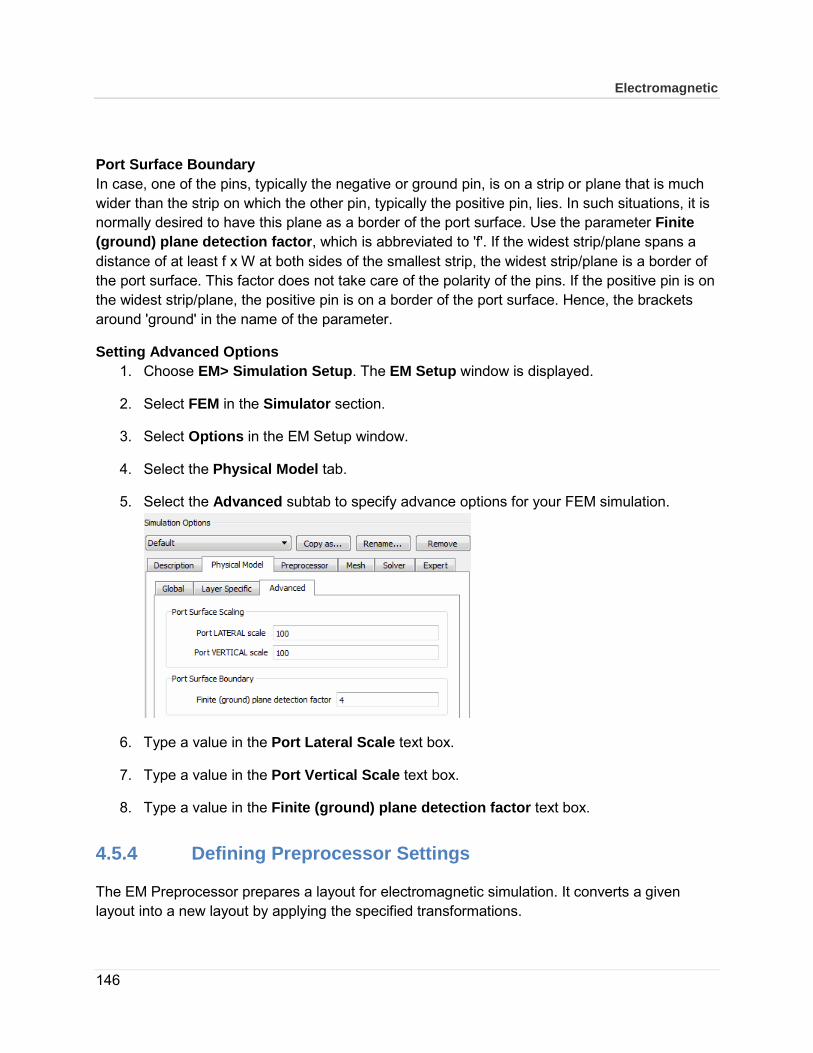
Electromagnetic
146
Port Surface Boundary In case, one of the pins, typically the negative or ground pin, is on a strip or plane that is much wider than the strip on which the other pin, typically the positive pin, lies. In such situations, it is normally desired to have this plane as a border of the port surface. Use the parameter Finite (ground) plane detection factor, which is abbreviated to 'f'. If the widest strip/plane spans a distance of at least f x W at both sides of the smallest strip, the widest strip/plane is a border of the port surface. This factor does not take care of the polarity of the pins. If the positive pin is on the widest strip/plane, the positive pin is on a border of the port surface. Hence, the brackets around 'ground' in the name of the parameter.
Setting Advanced Options 1. Choose EM> Simulation Setup. The EM Setup window is displayed.
2. Select FEM in the Simulator section.
3. Select Options in the EM Setup window.
4. Select the Physical Model tab.
5. Select the Advanced subtab to specify advance options for your FEM simulation.
6. Type a value in the Port Lateral Scale text box.
7. Type a value in the Port Vertical Scale text box.
8. Type a value in the Finite (ground) plane detection factor text box.
4.5.4 Defining Preprocessor Settings
The EM Preprocessor prepares a layout for electromagnetic simulation. It converts a given layout into a new layout by applying the specified transformations.

147
EM Simulation Transformations Overview
The duration of an EM simulation with a conformal mesh is dependent on the number of edges in the mesh. This relation is superlinear. If the number of edges increases, the simulation time increases more than proportionally. Reducing the complexity of the mesh improves performance, especially for larger designs. Besides the complexity of the mesh, the quality of the mesh is also important. A mesh containing triangles with acute angles can lead to a reduced accuracy of the solution or even cause numerical issues while solving.
Specifying the Preprocessor Settings
To specify preprocessor settings:
1. Choose EM > Simulation Setup to open the EM Setup window.
2. Select Options in the EM Setup window.
3. Click the Preprocessor tab.
Note You can view a graphical representation of the available optional transformations by clicking Show Visual Aid.
4. Select Heal the layout and specify the required settings.
5. Select Merge shapes touching each other where possible to preserve the edges shared between adjacent shapes.

Electromagnetic
148
6. Select Simplify the layout to generate a conformal mesh containing minimum number of edges. Specify the required settings.
7. Select Generate and replace shapes on derived layers to enable the processing of derived layers.
8. Select Save Preprocessor Messages as a DRC Result to display the location-bound information and warning messages. Specify the required settings.
Preprocessor Options Overview
The preprocessor settings alter the way the EM meshers interpret the input layout geometries to improve the quality and complexity reduction of a generated mesh. You can write the preprocessed version of the layout to a new cell view. you can specify the following preprocessor options:
• Layout healing: Layout healing merges vertices and edges in close proximity. It corrects numerical issues in the layout that obstruct the creation of a high-quality conformal mesh. Layout healing:
o Closes unintentional gaps between adjacent shapes that are frequently created by layout generators and import or export processes, as shown in the following figure:
o Ensures that stacked vias have only one joint boundary instead of two nearly identical boundaries, as shown in the following figure:
o Eliminates acute angles, as shown in the following figure:
o Defining snap distance: Within the same substrate layer, the vertices and edges that are closer together than the snap distance distance are merged. The

149
distances for layout healing are calculated using the L ∞ metric. In this metric, the distance between two points is the largest absolute difference between both horizontal and between both vertical components. Any set of points equidistant to a given point is an axis-aligned square. Distances calculated using the L ∞ metric always amount to a fraction between 1/√2 and 1 of the Euclidean distance.
The layout healing algorithm starts from an empty layout and inserts all edges of all polygons and polylines one by one. The stack of substrate layers is processed from top to bottom. Within one substrate layer, longer edges are inserted before shorter edges. Newly inserted edges merge with already present features on the same substrate layer within the snap distance. You can define automatic snap distance that enables the preprocessor to automatically provide a snap distance. Layout healing is enabled in this mode by default.
• Merge shapes touching each other where possible: This EM transformation merge the shapes that are touching each other in the design. In this type of transformation, shared edges in the are not preserved. The following figure displays an example of such transformation:
In an FEM simulation setup, you can specify three types of merge options: Merge Adjacent Layers with same Material Properties option in the Physical Model tab, Merge shapes touching each other where possible in the Preprocessor tab, and Merge Objects with Same Material in the Advanced subtab of the Mesh tab. The Preprocessor merge is done first. Layout objects, drawn on the same layer, touching each other are merged. Shared edges are not preserved during mesh generation. The merge option in the Physical Model merges adjacent layers that share the same material properties. Finally, during FEM mesh generation, and after the 3D objects are added if any, another merge can happen, based on material properties.
• Layout simplification: This EM transformation replaces polygons by nearly identical polygons with less vertices. The main purpose is to generate a conformal mesh containing minimum number of edges. Layout simplification also creates higher quality
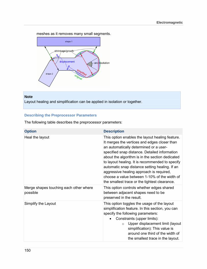
Electromagnetic
150
meshes as it removes many small segments.
Note Layout healing and simplification can be applied in isolation or together.
Describing the Preprocessor Parameters
The following table describes the preprocessor parameters:
Option Description Heal the layout This option enables the layout healing feature.
It merges the vertices and edges closer than an automatically determined or a user-specified snap distance. Detailed information about the algorithm is in the section dedicated to layout healing. It is recommended to specify automatic snap distance setting healing. If an aggressive healing approach is required, choose a value between 1-10% of the width of the smallest trace or the tightest clearance.
Merge shapes touching each other where possible
This option controls whether edges shared between adjacent shapes need to be preserved in the result.
Simplify the Layout This option toggles the usage of the layout simplification feature. In this section, you can specify the following parameters:
• Constraints (upper limits): o Upper displacement limit (layout
simplification): This value is around one third of the width of the smallest trace in the layout.

151
Option Description o Upper shrinkage/growth limit
(layout simplification): The reasonable values are in the range of 5 to 15%. For specific requirements, such as via simplification, the values up to 30-50% can be acceptable (this reduces circles to squares or triangles).
• Use different constraints for vias: You may need to simplify the vias more than the rest of the layout. You can specify a different set of constraints for vias: Displacement and Shrinkage/growth limit.
Save Preprocessor Messages as a DRC Result
This option enables you to display the location-bound information and warning messages in the layout using the DRC Results Viewer. The name of the DRC Result and the ADS layer where errors are shown can be configured.
Guidelines for Defining Preprocessor Settings
While defining the preprocessor parameters, you can refer the following guidelines:
• Layout healing can change the layout topology. Therefore, the healing algorithm is designed to make small changes to the layout topology. It is important to keep the snap distance below the minimal clearance between different layout nets, otherwise short circuits might appear. The snap distance must also be smaller than the width of thin layout traces, otherwise these traces will disappear.
• Specify a snap distance at least 10 times smaller than the minimal clearance and trace width.
• Whenever layout healing performs an actual layout change, a warning is displayed in the status window. The details of the change are written to the DRC Result or the layout processing report (dependent on the setup option Save preprocessor messages as a DRC Result). Refer the DRC result or the layout processing report to verify these changes.

Electromagnetic
152
• Do not use layout healing as a polygon simplification tool. It is recommended to avoid choosing a large snap distance. For this purpose, the layout simplification feature provides a better and safe alternative.
Generating Preprocessed Geometry
Before simulating your design, you can preprocess your design to automatically perform layout healing, merge shapes, and simplify the layout. To generate a preprocessed geometry:
1. Select Preprocessed geometry from the Generate drop-down list in the EM Setup window.
2. Click Go.
4.5.5 Defining Mesh Settings for Momentum
In the Momentum solution approach, any electromagnetic configuration of a 3D design can be represented without loss of generality as a voltage/current distribution on its surfaces. This continuous distribution is approximated by a finite number of unknowns using a mesh. This mesh is a grid-like pattern of triangular and/or quadrilateral cells tessellating all surfaces.
In an S-parameter simulation, coupling effects between cells are being calculated using the Green function database. The currents passing through mesh edges are then derived from mesh cell voltages to match the calculated coupling effects. From these results, S-parameters are calculated for the circuit.
The quality of the mesh determines the quality of a solution. The cells need to be small enough in order to capture real world spatial variations of the current/voltage distribution. However, covering low-variability regions with larger cells is necessary to keep the problem size within reasonable limits.
The default configuration of the mesh generator produces suitable meshes in the vast majority of situations. When desired, this configuration can be adjusted through a number user-adjustable parameters. The default parameters are used automatically. The mesh is normally

153
computed as part of the simulation process; no specific user intervention is required. It is also possible to explicitly preview the mesh without simulating in order to assess its quality.
Defining a Mesh
A mesh is a grid-like pattern of triangles and rectangles, and each triangle or rectangle is a cell. This pattern of cells is based on the geometry of a circuit and, optionally, user-defined parameters, so each circuit will have a unique mesh calculated for it. The mesh is then applied to the circuit in order to compute the current within each cell and identify any coupling effects in the circuit during simulation. From these calculations, S-parameters are then calculated for the circuit. The mesh that was calculated for the double patch example is shown below.
Creating a mesh consists of two parts:
• Defining mesh parameters
• Previewing the mesh It is not necessary to set up mesh parameters; default parameters will be used instead. You can preview the mesh before simulating in order to view the mesh, otherwise the mesh will be computed as part of the simulation process. A mesh is required in order to simulate.
You can define mesh parameters for the following areas:
• Entire circuit
• Objects on a layout layer
• Shape of an object
Note It is not necessary to specify parameters for all levels. For example, you can specify mesh parameters for a single object and use default values for the rest of the circuit.

Electromagnetic
154
Adjusting Mesh Density
A minimal mesh density is guaranteed by enforcing all cells to be smaller than a certain maximum cell size limit. When this maximum cell size is not stated explicitly, it is calculated from the mesh frequency and the number of cells per wavelength. The cells need to be small enough in order to capture real world spatial variations of the longitudinal current distribution. The spatial extent of waves is shortest at the highest frequency. Consider wave phenomena to be described by a sinusoid of a certain wavelength. Each mesh cell is able to approximate only the portion of the sinusoid it covers with a linear function. The accuracy of this piecewise linear fit improves as the number of cells per wavelength increases. For example, if you use 30 cells per wavelength, the maximum deviation between the sinusoid and the linear approximation is about 1 percent.
Increasing either the mesh frequency or the number of cells per wavelength makes the mesh denser. When a denser mesh is desired, it is generally better to increase the number of cells per wavelength than the mesh frequency. The optimal value for the mesh frequency is the highest simulation frequency that will be eventually used. In fact, an increase of the mesh frequency may trigger a recalculation or extension of the Green's functions database.
Note Only the maximal cell size is enforced and not the minimal cell size. A polygon with N sides can be tessellated with no less than N-2 triangles (or half as many quadrilaterals). This imposes a minimal cell size dependent on the level of detail of the geometry. Sometimes the geometric detail is much smaller than a fraction of the wavelength (typically when including integrated circuits in the simulation). In this case it is advised to choose an explicit maximal cell size not larger than four times the regular trace width. Otherwise the mesh may contain cells with a very large aspect ratio that cannot properly model the actual current flow.
Effect of Mesh Reduction on Simulation Accuracy
Mesh reduction is a technology that aims at removing mesh complexity originating from the meshing of geometrically complex shapes. In a normal situation, you specify the mesh density (the number of cells per wavelength) that needs to be used in the simulation in order to obtain a specific accuracy. However, due to geometrical constraints, the mesher can be forced to use more cells than strictly needed by the wavelength criterion. In this case, the mesh introduces "redundant" degrees of freedom in the solution process ("redundant" with respect to the electromagnetic behavior). Mesh reduction is a technology that automatically removes these redundant degrees of freedom, prior to the solution of the problem. Hence, it should have a negligible impact on the accuracy of the results.
Warning

155
Mesh reduction currently ignores layer or shape-specific mesh density settings. If you have other than global mesh settings, disable mesh reduction.
About the Edge Mesh
The edge mesh feature automatically creates a relatively dense mesh pattern of small cells along the edges of metal or slots, and a less dense mesh pattern of a few large cells in all other areas of the geometry. Because most of the current flow occurs along the edges of slots or metals, the edge mesh provides an efficient solution with greater accuracy.
Use the edge mesh to improve simulation accuracy when solving circuits where the modeling of current flow in any edge area is a critical part of the solution. This includes circuits where the characteristic impedance, or the propagation constant are critical for determining the electrical model, circuits in which close proximity coupling occurs, or circuits where edge currents dominate the circuit behavior. The following applications use the edge mesh:
• Tightly coupled lines
• Patch antennas
• Resonant circuits
• Delay lines
• Hairpin filters
Note Edge mesh is available at all levels of meshing: global, layout layer, and object meshing.
Setting the Width of the Edge Mesh
When using an edge mesh, choose Auto-determine Edge Width to let Momentum determine an appropriate width. Alternatively, enter an explicit width. To this end you can use Insert > Measure... to measure distances on the layout.
About the Transmission Line Mesh Use the transmission line mesh when you want to explicitly specify the number of cells in the direction perpendicular to the current flow. This has no effect on the mesh density in the direction of the current flow.
This setting can be used to improve the accuracy of a simulation with a coarse mesh density. For example, the simulation results for a single transmission line with one or two cells across its width will be equal. If you have coupled lines, the results will differ.
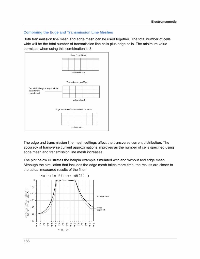
Electromagnetic
156
Combining the Edge and Transmission Line Meshes
Both transmission line mesh and edge mesh can be used together. The total number of cells wide will be the total number of transmission line cells plus edge cells. The minimum value permitted when using this combination is 3.
The edge and transmission line mesh settings affect the transverse current distribution. The accuracy of transverse current approximations improves as the number of cells specified using edge mesh and transmission line mesh increases.
The plot below illustrates the hairpin example simulated with and without and edge mesh. Although the simulation that includes the edge mesh takes more time, the results are closer to the actual measured results of the filter.

157
Processing Object Overlap
The parameter Thin layer overlap extraction should be used in designs that have thin layers in-between overlapping objects. It is possible that mesh cells are generated that cross the overlap region and this is not desirable. Typical situations where this is important are:
• Parallel plate capacitor: The charge will be accumulated where the plates overlap. Just next to that overlap area, charge will be much lower. As charge is assumed to be uniformly distributed on a mesh cell, when such cell crosses the plate overlap area, the charge will be spread out too much, resulting in a less accurate capacitance extraction.
• Transmission line above a finite ground plane: The return current in the ground plane will concentrate just under the transmission line at higher frequencies. Large mesh cells under the transmission line do not allow to describe that return current flow accurately. The overlap extraction provides a way to force a mesh that follows the shape of the transmission line allowing a more accurate approximation of the return current flow.
As an example, consider two layers, one above the other, and close together. They carry a large charge density where they overlap, which increases proportionally to 1/distance. If there is no metal above the layers, the charge density is nearly zero where there is no overlap, and the change is very rapid-nearly a step-at the point of overlap.
If no overlap extraction is performed, the mesher can create cells that will cross the border of the overlap. In the actual circuit, this cell would have a partially high charge density area where the overlap is present, and a partially low charge density area where there is no overlap. However, Momentum simulates cells with a constant charge density, and approximating the strongly-varying charge in the cell with a constant is not an adequate representation. Thus, by enabling thin layer extraction, no cells will be created that cross an overlap region.
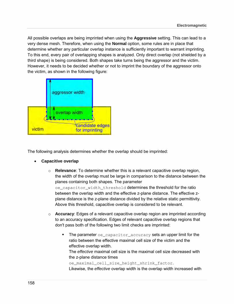
Electromagnetic
158
All possible overlaps are being imprinted when using the Aggressive setting. This can lead to a very dense mesh. Therefore, when using the Normal option, some rules are in place that determine whether any particular overlap instance is sufficiently important to warrant imprinting. To this end, every pair of overlapping shapes is analyzed. Only direct overlap (not shielded by a third shape) is being considered. Both shapes take turns being the aggressor and the victim. However, it needs to be decided whether or not to imprint the boundary of the aggressor onto the victim, as shown in the following figure:
The following analysis determines whether the overlap should be imprinted:
• Capacitive overlap
o Relevance: To determine whether this is a relevant capacitive overlap region, the width of the overlap must be large in comparison to the distance between the planes containing both shapes. The parameter oe_capacitor_width_threshold determines the threshold for the ratio between the overlap width and the effective z-plane distance. The effective z-plane distance is the z-plane distance divided by the relative static permittivity. Above this threshold, capacitive overlap is considered to be relevant.
o Accuracy: Edges of a relevant capacitive overlap region are imprinted according to an accuracy specification. Edges of relevant capacitive overlap regions that don't pass both of the following two limit checks are imprinted:
The parameter oe_capacitor_accuracy sets an upper limit for the ratio between the effective maximal cell size of the victim and the effective overlap width. The effective maximal cell size is the maximal cell size decreased with the z-plane distance times oe_maximal_cell_size_height_shrink_factor. Likewise, the effective overlap width is the overlap width increased with

159
the z-plane distance times oe_overlap_width_height_grow_factor.
The product of the parameters oe_capacitor_accuracy and oe_capacitor_inv_rel_sens_to_delta_w_div_eff_h sets an upper limit for the ratio between the maximal cell size and the effective z-plane distance.
• Inductive overlap
o Relevance: Only sufficiently long boundaries are considered for inductive overlap. The length of the boundary must exceed inductor_length_threshold times the minimal wavelength. In addition, the ratio of the overlap width to the aggressor width must exceed oe_inductor_width_threshold.
o Accuracy: Edges of a relevant inductive overlap region are imprinted according to an accuracy specification. The parameter oe_inductor_accuracy determines the threshold for the ratio between the effective maximal cell size of the victim and the effective overlap width. Above this threshold, edges of relevant inductive overlap regions are imprinted.
When an edge is being imprinted, it is allowed to snap to existing geometry if the snap distance is small enough to uphold the specified accuracy. This snap distance is additionally limited to oe_maximal_overlap_width_change times the overlap width.
The final Boolean parameter oe_pedantic can be used to impose the most strict overlap extraction rules. When enabled, it forces all other parameter values to zero. The Aggressive overlap extraction setting has been implemented in practice by forcing oe_pedantic to ON.
You can set all parameters by selecting Options > Expert in the EM Setup window. When unset, corresponding momentum.cfg configuration variables are consulted for default values. Finally, built-in default values are being used. These values guarantee proper overlap extraction across a wide range of designs.
The following table summarizes all overlap extraction related parameters. Note that all numerical parameters are dimensionless quantities.
Options > Expert key in EM Setup (highest priority)
$HOME/hpeesof/config/momentum.cfg variable name
permissible values built-in default value
oe_capacitor_width_threshold
MOM_MESHER_OVERLAP_EXTRACTION_DEFAULT_CAPACITOR_WIDTH_THRESHOLD
not negative 15
oe_capacitor_accu MOM_MESHER_OVERLA not negative 0.05
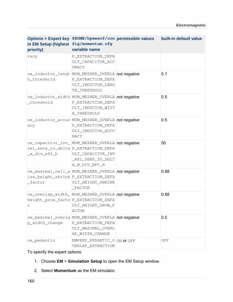
Electromagnetic
160
Options > Expert key in EM Setup (highest priority)
$HOME/hpeesof/config/momentum.cfg variable name
permissible values built-in default value
racy P_EXTRACTION_DEFAULT_CAPACITOR_ACCURACY
oe_inductor_length_threshold
MOM_MESHER_OVERLAP_EXTRACTION_DEFAULT_INDUCTOR_LENGTH_THRESHOLD
not negative 0.1
oe_inductor_width_threshold
MOM_MESHER_OVERLAP_EXTRACTION_DEFAULT_INDUCTOR_WIDTH_THRESHOLD
not negative 0.5
oe_inductor_accuracy
MOM_MESHER_OVERLAP_EXTRACTION_DEFAULT_INDUCTOR_ACCURACY
not negative 0.5
oe_capacitor_inv_rel_sens_to_delta_w_div_eff_h
MOM_MESHER_OVERLAP_EXTRACTION_DEFAULT_CAPACITOR_INV_REL_SENS_TO_DELTA_W_DIV_EFF_H
not negative 50
oe_maximal_cell_size_height_shrink_factor
MOM_MESHER_OVERLAP_EXTRACTION_DEFAULT_HEIGHT_SHRINK_FACTOR
not negative 0.88
oe_overlap_width_height_grow_factor
MOM_MESHER_OVERLAP_EXTRACTION_DEFAULT_HEIGHT_GROW_FACTOR
not negative 0.88
oe_maximal_overlap_width_change
MOM_MESHER_OVERLAP_EXTRACTION_DEFAULT_MAXIMAL_OVERLAP_WIDTH_CHANGE
not negative 0.5
oe_pedantic EMPREP_PEDANTIC_OVERLAP_EXTRACTION
ON or OFF OFF
To specify the expert options:
1. Choose EM > Simulation Setup to open the EM Setup window.
2. Select Momentum as the EM simulator.
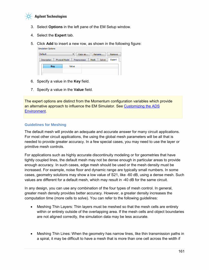
161
3. Select Options in the left pane of the EM Setup window.
4. Select the Expert tab.
5. Click Add to insert a new row, as shown in the following figure:
6. Specify a value in the Key field.
7. Specify a value in the Value field.
The expert options are distinct from the Momentum configuration variables which provide an alternative approach to influence the EM Simulator. See Customizing the ADS Environment.
Guidelines for Meshing
The default mesh will provide an adequate and accurate answer for many circuit applications. For most other circuit applications, the using the global mesh parameters will be all that is needed to provide greater accuracy. In a few special cases, you may need to use the layer or primitive mesh controls.
For applications such as highly accurate discontinuity modeling or for geometries that have tightly coupled lines, the default mesh may not be dense enough in particular areas to provide enough accuracy. In such cases, edge mesh should be used or the mesh density must be increased. For example, noise floor and dynamic range are typically small numbers. In some cases, geometry solutions may show a low value of S21, like -60 dB, using a dense mesh. Such values are different for a default mesh, which may result in -40 dB for the same circuit.
In any design, you can use any combination of the four types of mesh control. In general, greater mesh density provides better accuracy. However, a greater density increases the computation time (more cells to solve). You can refer to the following guidelines:
• Meshing Thin Layers: Thin layers must be meshed so that the mesh cells are entirely within or entirely outside of the overlapping area. If the mesh cells and object boundaries are not aligned correctly, the simulation data may be less accurate.
• Meshing Thin Lines: When the geometry has narrow lines, like thin transmission paths in a spiral, it may be difficult to have a mesh that is more than one cell across the width if

Electromagnetic
162
the default global mesh is used. If needed, use Edge Mesh or Transmission Line Mesh to capture the current distribution across the line.
• Meshing Slots: Slots should be meshed exactly the same as strips-there is no difference. For example, the edge mesh can be used for slots because the current distribution is basically the same, that is, it is concentrated on the edges of a slot.
• Adjusting the Mesh Density of Curved Objects: Vias or other curved objects, when drawn in a layout, have a default value for the number of facets used to draw the object, based on the command Options > Preferences > Entry/Edit > Arc/Circle Resolution (degrees). If the value is small, a relatively large number of facets are used to draw the circle, and this can result in more triangular cells created the curved areas during the mesh process. To change the number of facets for all arcs and circles, use the command shown above. To change them for a single object, select the object, then choose Edit > Modify > Arc/Circle Resolution. Then, increase the number of degrees for the radius, as required, to reduce the number of triangles. However, this alters the geometry of a circuit.
Defining Global Mesh Parameters
Global mesh parameters affect the entire circuit. To set up global parameters:
1. Select EM> Simulation Setup to open the EM Setup window.
2. Select Momentum as the EM simulator.
3. Select Options in the left pane of the EM Setup window.
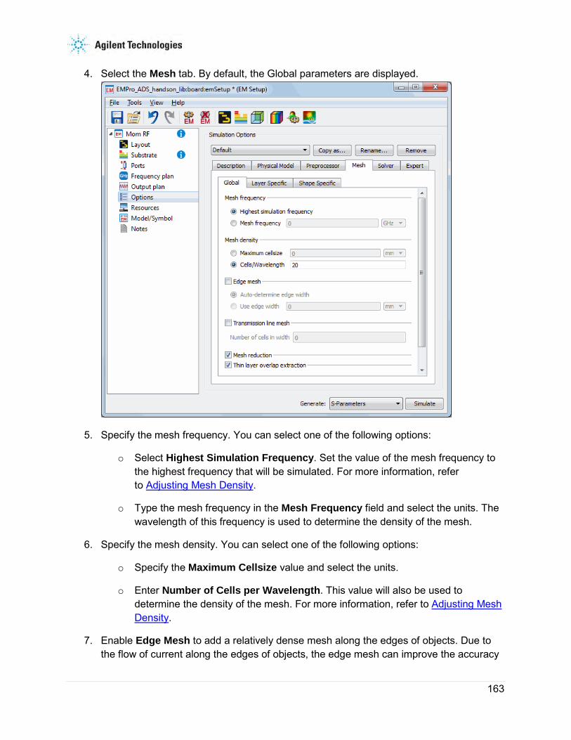
163
4. Select the Mesh tab. By default, the Global parameters are displayed.
5. Specify the mesh frequency. You can select one of the following options:
o Select Highest Simulation Frequency. Set the value of the mesh frequency to the highest frequency that will be simulated. For more information, refer to Adjusting Mesh Density.
o Type the mesh frequency in the Mesh Frequency field and select the units. The wavelength of this frequency is used to determine the density of the mesh.
6. Specify the mesh density. You can select one of the following options:
o Specify the Maximum Cellsize value and select the units.
o Enter Number of Cells per Wavelength. This value will also be used to determine the density of the mesh. For more information, refer to Adjusting Mesh Density.
7. Enable Edge Mesh to add a relatively dense mesh along the edges of objects. Due to the flow of current along the edges of objects, the edge mesh can improve the accuracy

Electromagnetic
164
and speed of a simulation. An edge mesh will similarly be created on thick conductor side walls. You can select one of the following options:
o If you want the edge mesh to be sized automatically, select Auto-determine Edge Width.
o To specify the edge width, select Edge Width and select the units. For more information about the edge mesh, refer to About the Edge Mesh.
Note An edge mesh that is specified with a width larger than the cell size set by the wavelength/number_of_cells_wavelength, will be ignored. This is because such edge meshes would be very inefficient. However, if these edge mesh values must be used, you can decrease the number_of_cells_wavelength, which is specified in the Number of Cells per Wavelength field.
8. Enable Transmission Line Mesh to specify the number of cells along the width of a geometry. This option is most useful for circuits with straight-line geometry.
9. Enter the number of cells that the width will be divided into in the Number of Cells Wide field. This will be the total number of cells along the width of the circuit. For more information about the transmission mesh, refer to About the Transmission Line Mesh.
10. Enable Mesh reduction to obtain an optimal mesh with fewer small cells and an improved memory usage and simulation time.
11. Enable Thin layer overlap extraction to extract objects for the following situations:
o Two objects on different layers overlap.
o The objects are separated with a thin substrate layer. If this is enabled, the geometry will be altered to produce a more accurate model for the overlap region. The Normal setting is recommended for most layouts. The Aggressive setting is only recommended when tiny overlap differences are expected to lead to significant result variations as this option will considerably increase the problem size. For more information, refer to Processing Object Overlap.
Note This should always be enabled for modeling thin layer capacitors.

165
Specifying Layer-specific Mesh Options
You can use the Layer Specific tab to define the mesh options for a specific layer. Perform the following steps:
1. Select EM> Simulation Setup to open the EM Setup window.
2. Select Momentum as the EM simulator.
3. Select Options in the EM Setup window.
4. Select the Mesh tab to display the mesh options for Momentum.
5. Select the Layer Specific subtab to specify settings at the layer level, as shown in the following figure:
6. Select a value from the Mesh Density drop-down list in the required layer.
7. Select a value from the Edge Mesh Width drop-down list in the required layer.
8. Select a value from the Transmission Line Mesh Width drop-down list in the required layer.
Specifying Shape-specific Mesh Options
You can customize the selected shape by using the Shape Specific tab. Perform the following steps:
1. Choose EM> Simulation Setup to open the EM Setup window.
2. Select Momentum as the EM simulator.
3. Select Options in the left pane of the EM Setup window.
4. Select the Mesh tab to display the mesh options for Momentum.
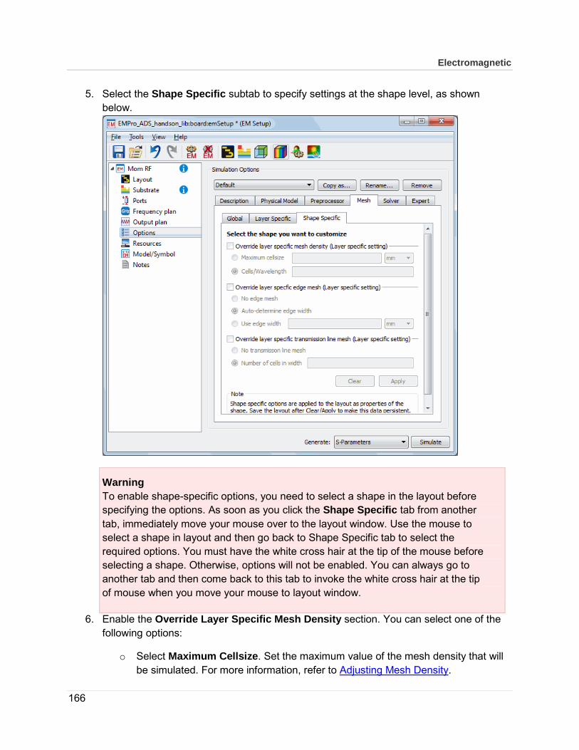
Electromagnetic
166
5. Select the Shape Specific subtab to specify settings at the shape level, as shown below.
Warning To enable shape-specific options, you need to select a shape in the layout before specifying the options. As soon as you click the Shape Specific tab from another tab, immediately move your mouse over to the layout window. Use the mouse to select a shape in layout and then go back to Shape Specific tab to select the required options. You must have the white cross hair at the tip of the mouse before selecting a shape. Otherwise, options will not be enabled. You can always go to another tab and then come back to this tab to invoke the white cross hair at the tip of mouse when you move your mouse to layout window.
6. Enable the Override Layer Specific Mesh Density section. You can select one of the following options:
o Select Maximum Cellsize. Set the maximum value of the mesh density that will be simulated. For more information, refer to Adjusting Mesh Density.
167
o Type the number of cells per wavelength in the Cells/Wavelength text box.
7. Enable Override Layer Specific Edge Mesh. You can select one of the following options:
o No Edge Mesh
o Auto-determine Edge Width
o Use Edge Width
8. Enable the Override Layer Specific Transmission Line Mesh section. You can select one of the following options:
o No Transmission Line Mesh
o Cells in Width
4.5.6 Defining Mesh Settings for FEM
To perform a FEM simulation, the entire 3D problem domain is divided into a set of tetrahedra (or cells). The pattern of cells, called the mesh, is based on the geometry of a layout and optionally, user-defined parameters, so each layout has a unique mesh calculated for it. The mesh is then applied to the geometry to compute the electric fields within each cell. It also helps to identify any coupling effects in the layout during simulation. From these calculations, S-parameters are then calculated for the layout.
The FEM simulator implements an adaptive meshing algorithm, where an initial mesh is generated and the electric fields (and S-parameters) are computed on that initial mesh for a single frequency or multiple frequencies if Performing FEM Broadband Refinement is used. An error estimate is generated for each tetrahedron. The tetrahedrons with the largest estimated errors are refined to create a new mesh where the electric fields (and S-parameters) are computed again. The S-parameters from consecutive meshes are compared. If the S-parameters do not change significantly, then electric fields (and S-parameters) are computed for all the requested frequencies. If the S-parameters do change significantly, then new error estimates are computed, a new mesh is generated and new electric fields (and S-parameters) are computed.
Specifying Mesh Settings for FEM
To define FEM mesh settings using the EM Setup window:
1. Select EM > Simulation Setup to open the EM Setup window.
2. Select the FEM simulator.
3. Select Options in the left pane of the EM Setup window.

Electromagnetic
168
4. Click the Mesh tab, as shown in the following figure:
In the Mesh tab, you can specify the following settings:
• Specifying Stop Criterium Settings
• Specifying Refinement Settings
• Specifying Initial Mesh Settings
• Specifying Advanced Settings
Specifying Stop Criterium Settings
Using the Stop criterium tab, you can specify delta error and adaptive phase values. The following figure displays the stop criterium options:

169
The following table describes the stop criterium options:
Option Description Delta Error Global Delta S-parameter sets a value that is
applied to all S-parameters in the solution. Enter a value in the Delta Error field. It is the allowable change in the magnitude of the vector difference for all S-parameters for at least the number of consecutive refinement passes specified in the field "Consecutive passes of delta error required".
Consecutive passes of delta error required Specify the required number of consecutive passes with a delta error smaller than or equal to the value specified in the field "Delta Error".
Minimum number of adaptive passes Enter the minimum number of refinement passes. The number of refinement passes is at least this number even if the convergence criterium based on the delta error is met with less refinement passes. If you have concerns about convergence, you can increase this value, otherwise, use the default value of 2.
Maximum number of adaptive passes Enter the maximum number of passes to be attempted. If the number of refinement passes entered is reached before the delta error criterium is met, the refinement process ends, based upon this limit. Typically, a value between 10 and 20 is recommended.
Use Memory Limit If the memory used by the FEM solver exceeds the specified memory limit, the mesh refinement process will end and the simulation will continue with the solve phase, even if the delta error does not satisfy the convergence
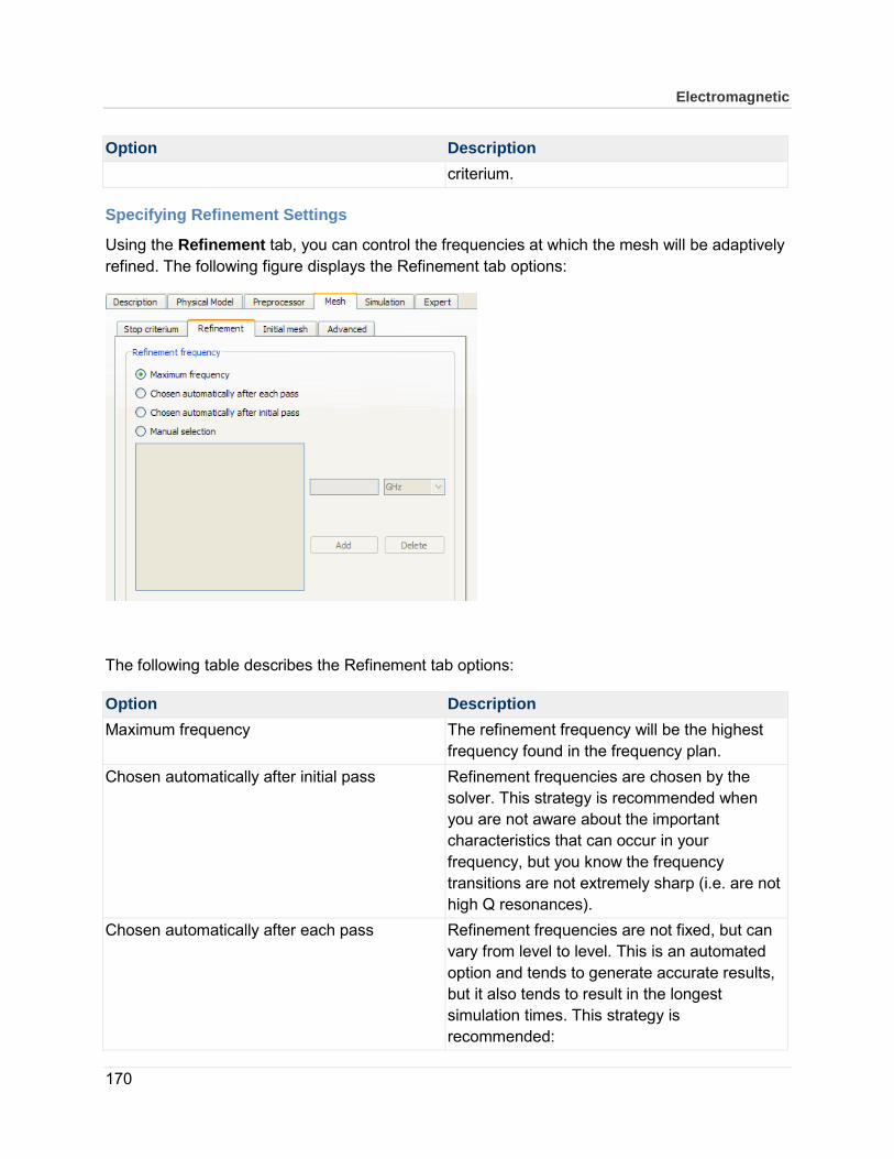
Electromagnetic
170
Option Description criterium.
Specifying Refinement Settings
Using the Refinement tab, you can control the frequencies at which the mesh will be adaptively refined. The following figure displays the Refinement tab options:
The following table describes the Refinement tab options:
Option Description Maximum frequency The refinement frequency will be the highest
frequency found in the frequency plan. Chosen automatically after initial pass Refinement frequencies are chosen by the
solver. This strategy is recommended when you are not aware about the important characteristics that can occur in your frequency, but you know the frequency transitions are not extremely sharp (i.e. are not high Q resonances).
Chosen automatically after each pass Refinement frequencies are not fixed, but can vary from level to level. This is an automated option and tends to generate accurate results, but it also tends to result in the longest simulation times. This strategy is recommended:

171
Option Description • For structures with high Q resonances. • During final analysis of a structure
where accuracy is preferred over fast simulations.
Manual Selection Refinement frequencies are specified
manually.
Performing FEM Broadband Refinement
Specifying Initial Mesh Settings
Using the Initial mesh tab settings, you can control how an initial mesh is generated. If the initial mesh is made finer, the adaptive mesh refinement may converge faster. However, a finer mesh results in higher computation times. Therefore, to avoid overmeshing, the intial mesh size should not be too small.
For some resonating structures, such as patch antennas, the adaptive refinement may fail to converge, if the initial mesh is not fine enough. This is because the resonance frequency depends heavily on the mesh and a small difference in this frequency causes a large delta S. In these cases, the initial mesh settings are required to get the adaptive refinement converging.
From ADS 2012 onwards, there are both global and layer-specific initial mesh settings.
Global Initial Mesh Settings Using the Global tab, you can set initial target size, automatic, and edge mesh length. The following figure displays the initial mesh options:

Electromagnetic
172
The following table describes the Global initial mesh tab options:
Option Description Use Initial Target mesh size Provides an initial denser mesh. If used, no
edge in the initial mesh will be longer than the given length. If you click Automatically Determine, the initial target mesh size is determined automatically. The length is computed based on the frequency plan available when the request is made.
Automatic Conductor Mesh When automatic conductor meshing is selected, the mesher estimates where mesh lengths need to be reduced to improve the accuracy and convergence speed of the simulation. The algorithm to produce this mesh is based on the DC connectivity of geometry with ports. Only parts electrically connected to a port are affected. For those parts the edge and vertex mesh is set. The length of the edge and vertex mesh is based on the estimated width assuming the structure being excited starts with a strip-like construction. The mesh process will report the estimated width in the simulation output window.
Conductor edge mesh length Specifies a target mesh size of all edges that belong to the geometry of a conductor. Edges do not necessarily have to be straight lines. A value of 0 means that no initial conductor edge mesh length is applied.
Conductor vertex mesh length Specifies a target mesh size for all vertices that belong to the geometry of a conductor. A value of 0 means that no initial conductor vertex mesh length is applied.
Number of bondwire segments Enables you to specify the number of bondwire segments.
Global Vertex Mesh Length Defines the value of the Global field used in Layer Specific Initial mesh tab
Global Edge Mesh Length Defines the value of the Global field used in Layer Specific Initial mesh tab

173
Option Description Global Surface Mesh Length Defines the value of the Global field used in
Layer Specific Initial mesh tab
To avoid difficult convergence during adaptive refinement and large number of unknowns, use the initial mesh options, Initial target mesh size and edge mesh size.
Layer-specific Initial Mesh Settings Using the Layer Specific tab, you can set the vertex, edge, and surface mesh options for each layer. The following figure displays the Layer Specific tab options:
If a mesh setting of a layer is set to <Global>, it will inherit its value from the corresponding global mesh setting on the Global Initial Mesh tab, which is also shown on the first row in the Layer Specific tab. It is also possible to enter a maximum cell size that differs from the global value. The value is then displayed in bold. A value of 0 always means that no initial mesh size is applied.
Vertex Mesh Vertex meshing reduces the mesh length around vertices. When combined with edge meshing the shortest length of both is chosen in any given region. The region where the value is applied by the vertex mesh length setting is roughly twice its length in each direction: the actual region is still being optimized. The region affected by it depends on local geometry.
The following figure displays the result of a vertex mesh setting:
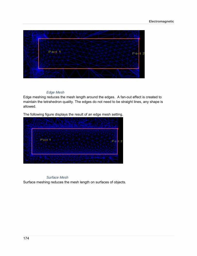
Electromagnetic
174
Edge Mesh Edge meshing reduces the mesh length around the edges. A fan-out effect is created to maintain the tetrahedron quality. The edges do not need to be straight lines, any shape is allowed.
The following figure displays the result of an edge mesh setting.
Surface Mesh Surface meshing reduces the mesh length on surfaces of objects.
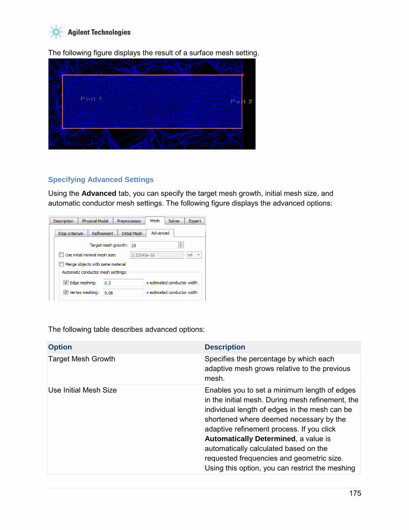
175
The following figure displays the result of a surface mesh setting.
Specifying Advanced Settings
Using the Advanced tab, you can specify the target mesh growth, initial mesh size, and automatic conductor mesh settings. The following figure displays the advanced options:
The following table describes advanced options:
Option Description Target Mesh Growth Specifies the percentage by which each
adaptive mesh grows relative to the previous mesh.
Use Initial Mesh Size Enables you to set a minimum length of edges in the initial mesh. During mesh refinement, the individual length of edges in the mesh can be shortened where deemed necessary by the adaptive refinement process. If you click Automatically Determined, a value is automatically calculated based on the requested frequencies and geometric size. Using this option, you can restrict the meshing
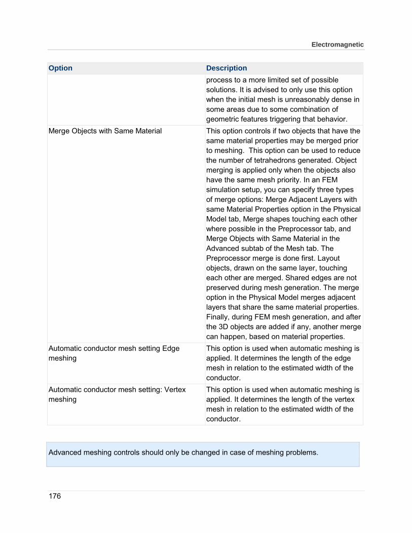
Electromagnetic
176
Option Description process to a more limited set of possible solutions. It is advised to only use this option when the initial mesh is unreasonably dense in some areas due to some combination of geometric features triggering that behavior.
Merge Objects with Same Material This option controls if two objects that have the same material properties may be merged prior to meshing. This option can be used to reduce the number of tetrahedrons generated. Object merging is applied only when the objects also have the same mesh priority. In an FEM simulation setup, you can specify three types of merge options: Merge Adjacent Layers with same Material Properties option in the Physical Model tab, Merge shapes touching each other where possible in the Preprocessor tab, and Merge Objects with Same Material in the Advanced subtab of the Mesh tab. The Preprocessor merge is done first. Layout objects, drawn on the same layer, touching each other are merged. Shared edges are not preserved during mesh generation. The merge option in the Physical Model merges adjacent layers that share the same material properties. Finally, during FEM mesh generation, and after the 3D objects are added if any, another merge can happen, based on material properties.
Automatic conductor mesh setting Edge meshing
This option is used when automatic meshing is applied. It determines the length of the edge mesh in relation to the estimated width of the conductor.
Automatic conductor mesh setting: Vertex meshing
This option is used when automatic meshing is applied. It determines the length of the vertex mesh in relation to the estimated width of the conductor.
Advanced meshing controls should only be changed in case of meshing problems.

177
4.5.7 Defining Solver Settings
You can define the solver settings for both Momentum and FEM. The simulation process combines the Green functions that were calculated for the substrate of a circuit and mesh information that was calculated for the circuit and solves for currents in the circuit. Using these current calculations, S-parameters are then calculated for the circuit.
Defining the Solver Settings for Momentum
You can select the following types of matrix solvers used by Momentum during a simulation:
• Auto-select: If you select the Auto-select solver, Momentum automatically selects the most appropriate matrix solver. It is the default matrix solver selection option.
• Direct Dense: If you select Direct dense, Momentum selects the direct dense matrix solver for a simulation. This implies that the matrix is stored in a dense matrix format (requiring order N2 memory) and solved using a direct matrix factorization technique (requiring order N3 computer time). The direct dense matrix solver guarantees to provide a solution using a predetermined number of operations. The main disadvantage is that the computer time it requires scales qubic with the matrix size N, yielding larger simulation times for large problem sizes.
• Iterative Dense: If you select Iterative dense, Momentum selects the iterative dense matrix solver for a simulation. This implies that the matrix is stored in a dense matrix format (requiring order N2 memory) and solved using an iterative matrix solve technology (requiring order N2 computer time). The computer time scales quadratic with the matrix size N, yielding faster simulation times for large problem sizes when compared to the direct dense matrix solver. The main disadvantage is that the iterative solver does not guarantee to converge fast. The iterative solver monitors its convergence rate and automatically switches to the Direct dense matrix solver when it observes that the convergence stagnates or the convergence rate is too slow.
• Direct Compressed matrix solver: When selecting Direct compressed, Momentum selects the direct compressed matrix solver to be used in the simulation. This implies that the matrix is stored in a compressed matrix format (requiring order NlogN memory) and solved using a direct compressed matrix factorization technique (requiring order (NlogN)1.5 computer time). The direct compressed matrix solver guarantees to always provide a solution using a predetermined number of operations. Moreover, the computer time it requires scales linear-logarithmic with the matrix size N, making it the preferred matrix solver for large problem sizes.
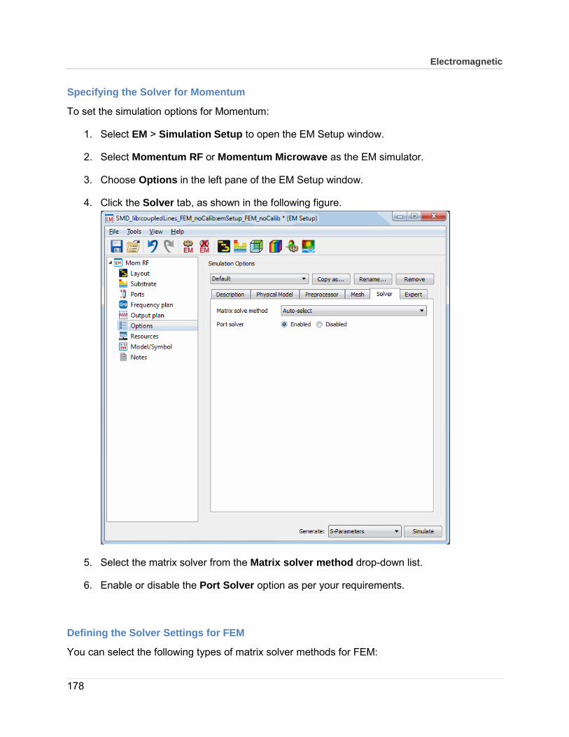
Electromagnetic
178
Specifying the Solver for Momentum
To set the simulation options for Momentum:
1. Select EM > Simulation Setup to open the EM Setup window.
2. Select Momentum RF or Momentum Microwave as the EM simulator.
3. Choose Options in the left pane of the EM Setup window.
4. Click the Solver tab, as shown in the following figure.
5. Select the matrix solver from the Matrix solver method drop-down list.
6. Enable or disable the Port Solver option as per your requirements.
Defining the Solver Settings for FEM
You can select the following types of matrix solver methods for FEM:
179
• Direct:When selecting Direct, the FEM Simulator chooses the direct sparse matrix solver to be used in the simulation.
• Iterative: When selecting Iterative, FEM Simulator chooses the iterative sparse matrix solver to be used in the simulation. There is a choice between two iterative solvers. The default iterative solver is multithreaded and yields better performance, particularly for larger designs. The legacy iterative solver (single-threaded) is also available, as this solver typically requires less memory (up to a factor 2).
You can also specify the Order of basis functions used to approximate the electric fields in all tetrahedra. You can set the following values:
• 2: Electric fields will be approximated with a quadratic variation in each tetrahedron, and the magnetic fields will be approximated with a linear variation in each tetrahedron. This gives the best accuracy.
• 1: Electric fields will be approximated with a linear variation in each tetrahedron, and the magnetic fields will be approximated as being constant in each tetrahedron. This requires less memory than the Order 2 basis functions given the same mesh, but typically requires a larger mesh to get the same level off accuracy. This setting is useful for electrically small structures.
The following simulation settings are available by clicking the Advanced button:
• Use Legacy Iterative Solver: Provides CPU multithreading enhancements to the iterative solver, resulting in a twice speed improvement on computers with quad-core CPUs. Note that the FEM direct solver also supports CPU multithreading.
• Maximal Number of Iterations: Specifies the maximum number of iterations allowed during the iterative solve process. This value is increased to achieve a lower absolute tolerance. Typically a value 500 is sufficient.
• Tolerance iterative solver: Specifies the absolute error tolerance that the solver process must reach to achieve convergence. A typical value would be 1.0e-5. You may need to increase the Maximum Number of Iterations if you significantly decrease the tolerance.
Specifying Simulation Settings for FEM
To set the simulation options for FEM:

Electromagnetic
180
1. Select EM > Simulation Setup to open the EM Setup window.
2. Select FEM as the EM simulator.
3. Choose Options in the left pane of the EM Setup window.
4. Click the Solver tab.
5. Select a matrix solver from the Matrix solver method drop-down list.
6. Select a value for the Order of basis functions field.
7. Click the Advanced tab to specify advanced simulation settings for FEM, as shown in the following figure:
8. Specify the Maximal Number of Iterations value.
9. Specify the Tolerance iterative solver value.
10. Select the Use Legacy Iterative Solver option to use the single-threaded iterative solver. Deselect the option to use the multi-threaded iterative solver.

181
4.5.8 Performing FEM Broadband Refinement
You can automate the FEM broadband refinement process. You can select one of the following refinement strategies depending on your requirements:
• Multiple fixed refinement frequencies
• Refinement frequencies chosen automatically after the initial pass
• Refinement frequencies chosen automatically after each pass
• Manual refinement frequency
This section describes the refinement frequencies and provides guidelines for choosing a strategy.
Importance of Refinement Frequencies
Mesh refinement procedures in FEM typically consist of the following steps:
1. Simulate at the refinement frequencies.
2. If the calculated S-parameters did not reach convergence, perform the following steps:
o Estimate the discretization errors of the field solution.
o Refine the mesh at locations with high values for the error.
o Repeat step 1.
In this procedure, the refinement frequencies play a key role:
• Convergence monitoring: the convergence of the refinement process is monitored at the refinement frequencies (step 2).
• Field error estimation: the field error estimates, on which mesh refinement is based, are calculated at the refinement frequencies (step 2a).
Consequently, the choice of the refinement frequencies can have an important impact on the accuracy of the simulation results:
• The mesh convergence is monitored at frequencies where the S-parameters change most during mesh refinement. If this is not the case, the refinement process might stop too early, i.e., before the mesh refinement has reached convergence over the entire frequency range of interest.
• All important electromagnetic phenomena should occur at one of the refinement frequencies. If this is not the case, this phenomena cannot be taken into account during

Electromagnetic
182
mesh refinement. As a consequence, it is possible that the final mesh is not suited to represent this phenomena accurately.
Choosing a Refinement Strategy in FEM You can select one of the following refinement strategies depending on your requirements:
• Select the maximum simulation frequency for the adaptive refinement
• Refinement frequencies chosen automatically after the initial pass of the adaptive refinement
• Refinement frequencies chosen automatically after each pass of the adaptive refinement
• Manual specification of one of more refinement frequencies
This section describes these refinement frequencies and provides guidelines for choosing a strategy.
Performing Automatic Broadband Refinement Multiple Fixed Refinement Frequencies
You can specify a set of refinement frequencies by selecting the button ‘Manual selection’, and adding frequencies to the frequency table. This refinement strategy behaves as follows:
• All refinement frequencies are simulated on each mesh level.
• Convergence is reached if the convergence criterium is satisfied for all refinement frequencies. In other words, convergence depends on the worst case refinement frequency on each level.
• The mesh refinement depends on the error estimates of all refinement frequencies.
The corresponding logfile shows:
• Delta(S) for each simulated frequency
• Worst case Delta(S) for each mesh level (last line)
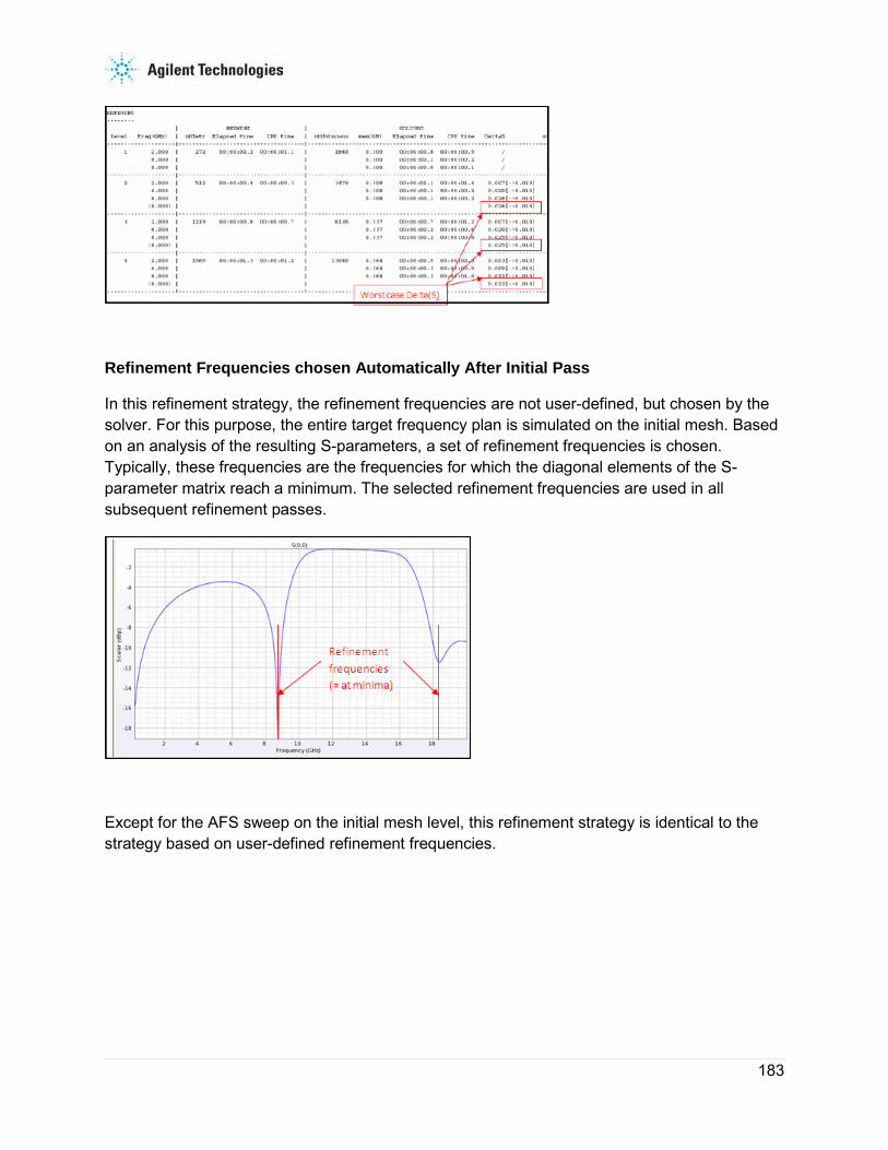
183
Refinement Frequencies chosen Automatically After Initial Pass
In this refinement strategy, the refinement frequencies are not user-defined, but chosen by the solver. For this purpose, the entire target frequency plan is simulated on the initial mesh. Based on an analysis of the resulting S-parameters, a set of refinement frequencies is chosen. Typically, these frequencies are the frequencies for which the diagonal elements of the S-parameter matrix reach a minimum. The selected refinement frequencies are used in all subsequent refinement passes.
Except for the AFS sweep on the initial mesh level, this refinement strategy is identical to the strategy based on user-defined refinement frequencies.

Electromagnetic
184
Refinement Frequencies Chosen Automatically After Each Pass
In this refinement strategy, the refinement frequencies are not fixed, but can vary from level to level. This refinement strategy behaves as follows:
• The entire target frequency plan is simulated on each mesh level using an adaptive frequency sweep.
• The difference of the S-parameters of the rational models is monitored, instead of the difference between the S-parameters of the simulated frequencies only. In other words, convergence depends on the worst case frequency in the entire frequency range of interest. This is the most detailed convergence monitoring possible.
• Mesh refinement depends on the error estimates of all simulated frequencies.

185
Selecting a Refinement Strategy You can refer the following guidelines while selecting a refinement strategy:
• Multiple fixed refinement frequencies: This strategy computes the fewest frequency points during the adaptive refinement stage and therefore usually lead to the fastest simulations. This strategy is recommended for:
o Electrically short transition structures. These can include matching networks, packages, and impedance transformations. If the transmission parameters accumulate less than 180 degrees of phase, it is sufficient to refine only at the highest frequency.
o Designs where you know the frequencies of the critical features such as dual (or multi) band antennas and band pass filters. For these structures set the refinement frequencies to the frequencies of most interest (i.e. in each antenna frequency band, at the low end and high end of the band pass filter). It is advisable to include the maximum frequency of the simulation as a refinement frequency.
o Initial analysis of a structure where speed is preferred over accuracy.
• Refinement frequencies chosen automatically after the initial pass: This strategy is a compromise between manually selecting the refinement frequencies and letting the FEM simulator automatically select the refinement frequencies at each adaptive pass. This strategy is recommended when you do not have a good idea where the important characteristics occur in your frequency. However, you might know the frequency transitions are not extremely sharp (i.e. are not high Q resonances).
• Refinement frequencies chosen automatically after each pass: This is the automated strategy and tends to generate accurate results, but it also tends to result in the longest simulation times. This strategy is recommended in the following situations:
o Structures with high Q resonances.
o During the final analysis of a structure where accuracy is preferred over fast simulations.
4.6 Generating an EM Model and Symbol An EM Model is used by a circuit simulator to model a component by using the S-parameters generated by an EM simulation. The EM-based S-parameters can be precomputed or you can generate them while running the circuit simulation. An EM Model caches the S-parameters to improve circuit simulation performance. For more information about how to use an EM model, see Using an EM Model.
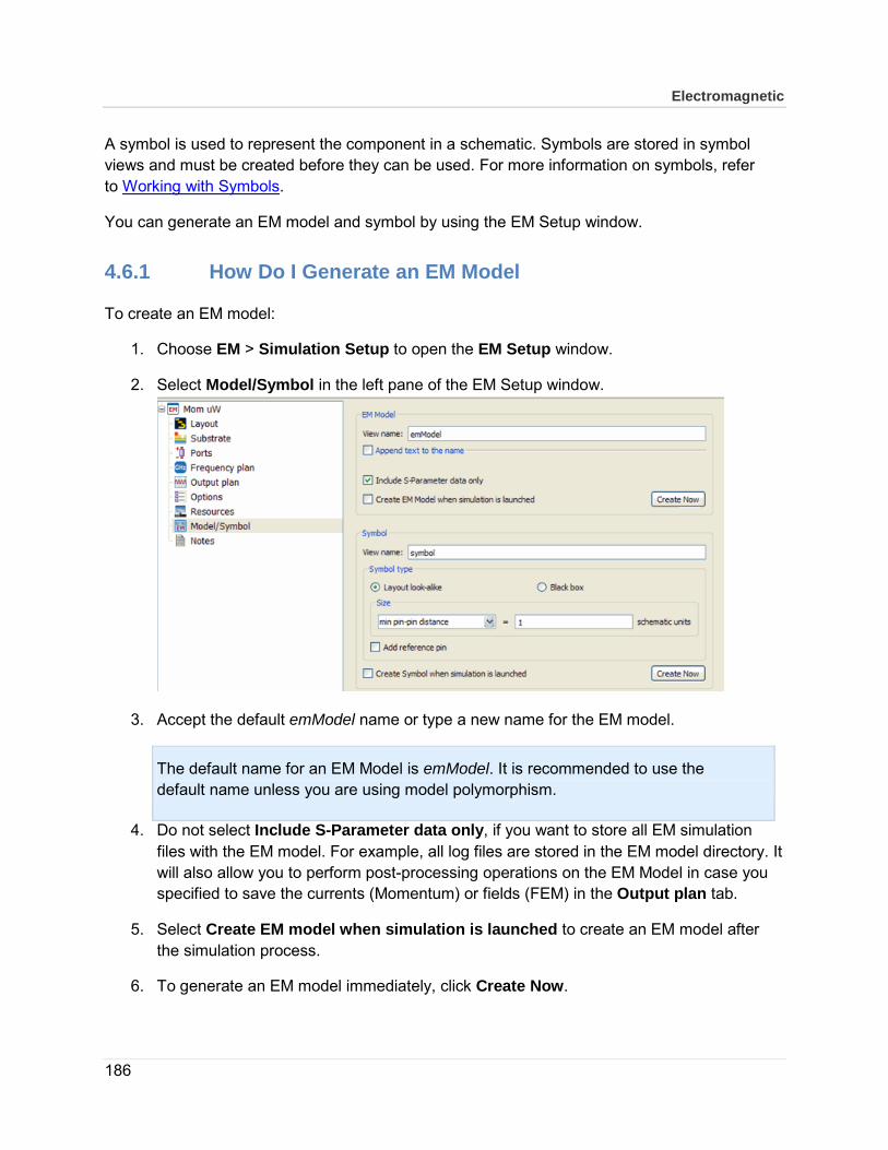
Electromagnetic
186
A symbol is used to represent the component in a schematic. Symbols are stored in symbol views and must be created before they can be used. For more information on symbols, refer to Working with Symbols.
You can generate an EM model and symbol by using the EM Setup window.
4.6.1 How Do I Generate an EM Model
To create an EM model:
1. Choose EM > Simulation Setup to open the EM Setup window.
2. Select Model/Symbol in the left pane of the EM Setup window.
3. Accept the default emModel name or type a new name for the EM model.
The default name for an EM Model is emModel. It is recommended to use the default name unless you are using model polymorphism.
4. Do not select Include S-Parameter data only, if you want to store all EM simulation files with the EM model. For example, all log files are stored in the EM model directory. It will also allow you to perform post-processing operations on the EM Model in case you specified to save the currents (Momentum) or fields (FEM) in the Output plan tab.
5. Select Create EM model when simulation is launched to create an EM model after the simulation process.
6. To generate an EM model immediately, click Create Now.

187
Note If the Create Now button is labeled Update Now, then the EM Model already exists for this cell.
The following figure displays an EM model:
You can also generate an EM model by selecting EM > Component > Create EM Model and Symbol. To know more about an EM Model, see Using an EM Model.
Customizing the EM Model Naming Convention
You can customize the naming convention of the EM model generated during a simulation by adding a prefix or suffix to the data name. To generate the EM model with the required naming convention, you need to specify the following parameters in the EM Setup dialog box:
• Specifying the EM model name: You can specify the EM model name in the Name field.
• Appending customized text to the EM model name: If you want to include customized text with the EM model name, select Append text to the name. You can customize the data name as follows:

Electromagnetic
188
o Adding text from the layout view: Select the View name option in the From the layout view section to add text from the layout view.
o Adding text from the simulation setup view: Select View name in the From the simulation setup view section to add text from the simulation setup view. You can also include the type of simulator in the EM model name by selecting Simulation Type.
o Adding user-defined text: You can add a suffix to the EM model name in the This text field.
To customize the EM model name:
1. Choose EM > Simulation Setup to open the EM Setup window.
2. Select Model/Symbol in the left pane of the EM Setup window.
3. Specify the EM model name in the Name field.
4. Select Append text to the name, as shown in the following figure:
5. Select View name in the From the layout view section.
6. Select View name in the From the simulation setup view section.
7. Select Simulation Type.
8. Add a suffix to the EM model name in the This text field.
4.6.2 Generating Symbols
A symbol is used to represent the component in a schematic. Symbols are stored in symbol views and must be created before they can be used.
The symbol created can either be a black box or a layout look-alike symbol.
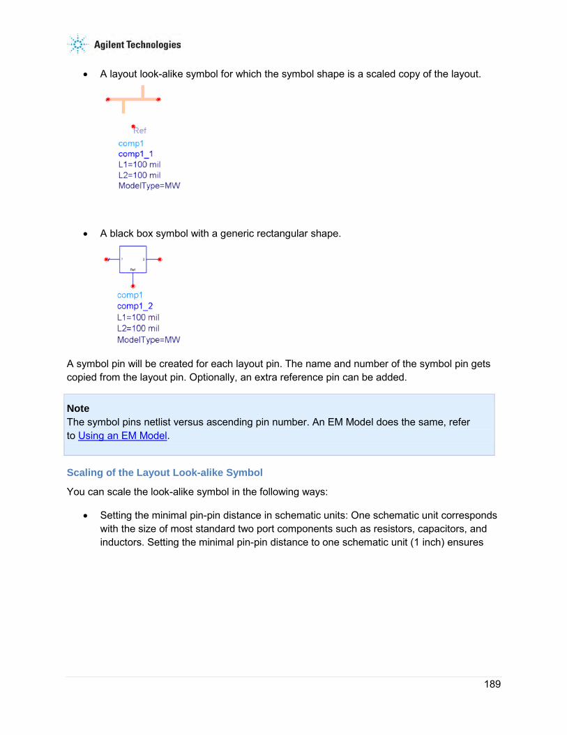
189
• A layout look-alike symbol for which the symbol shape is a scaled copy of the layout.
• A black box symbol with a generic rectangular shape.
A symbol pin will be created for each layout pin. The name and number of the symbol pin gets copied from the layout pin. Optionally, an extra reference pin can be added.
Note The symbol pins netlist versus ascending pin number. An EM Model does the same, refer to Using an EM Model.
Scaling of the Layout Look-alike Symbol
You can scale the look-alike symbol in the following ways:
• Setting the minimal pin-pin distance in schematic units: One schematic unit corresponds with the size of most standard two port components such as resistors, capacitors, and inductors. Setting the minimal pin-pin distance to one schematic unit (1 inch) ensures

Electromagnetic
190
that a component with a given symbol size will fit between two pins.
• Setting the maximum pin-pin distance in schematic units: The following figure illustrates the scaling when the maximal pin-pin distance is set to be equal to one schematic unit (1 inch).

191
• Mapping the layout unit dimensions to the schematic unit dimensions (recommended when combining different components in the same schematic page).
When you combine different layout components on a single schematic, a fixed, absolute scaling factor is the most appropriate choice to ensure that the relative sizes of the layout components are preserved.
Adding a Reference Pin
Using the Add Reference Pin check box, you can enable or disable the addition of an extra reference pin during layout component creation. This "extra" pin is used by EM to provide a reference voltage for all other pins in the layout and enables you to model ground effects (e.g., ground bounce, imperfect ground connections, etc.). In the absence of an explicit Reference Pin, this reference voltage is zero what corresponds with connecting the Reference Pin to the absolute ground (GROUND component) which gets netlisted as node 0.
The Add Reference Pin selection is only available for the layout look-alike symbol selection. When selecting black box this option gets enabled (grayed out). Because black box uses standard symbols, a reference pin will appear in all schematic black box representations. This can cause problems if you are creating a structure with finite ground planes and wish to use them in the schematic. In this case, the layout look-alike symbol with Add Reference Pin disabled is a better choice.
This option should also be disabled for components intended to be used with the Schematic > Generate/Update command. This extra pin will cause pin mismatch errors during design synchronization.
How Do I Create a Symbol
To create a symbol:
1. Choose EM > Simulation Setup to open the EM Setup window.
2. Select Model/Symbol in the left pane of the EM Setup window.
3. In the Symbol section, specify a name for the symbol.
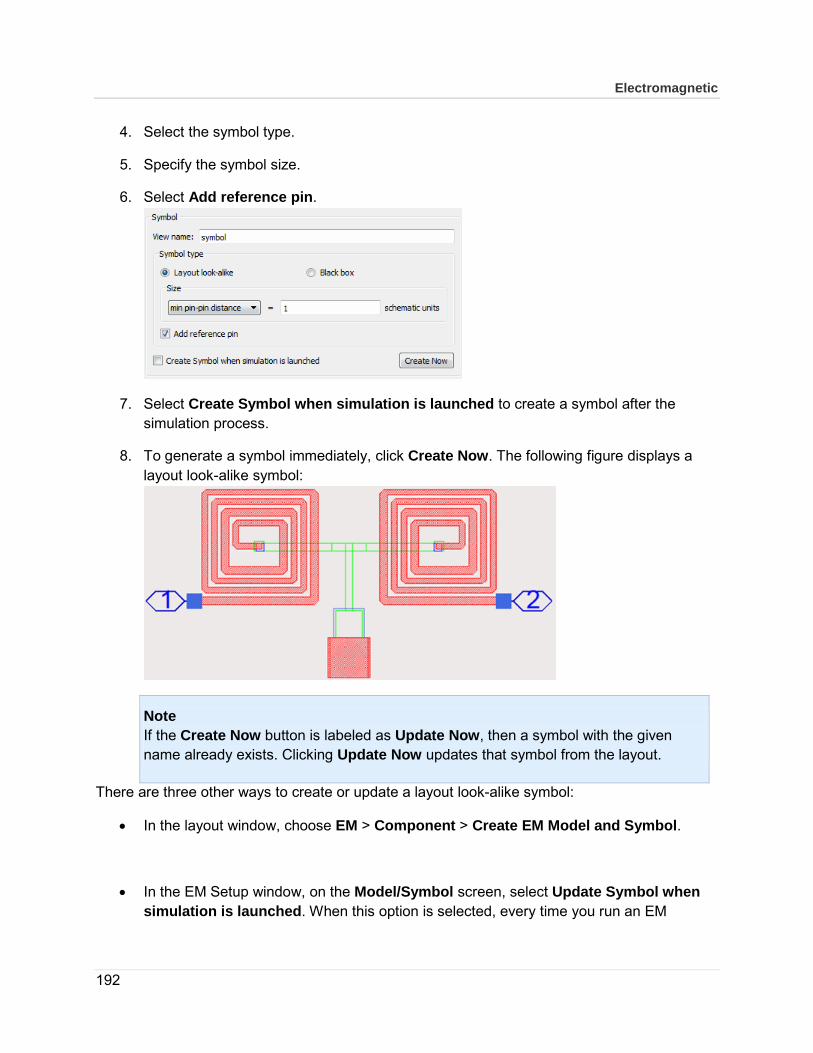
Electromagnetic
192
4. Select the symbol type.
5. Specify the symbol size.
6. Select Add reference pin.
7. Select Create Symbol when simulation is launched to create a symbol after the simulation process.
8. To generate a symbol immediately, click Create Now. The following figure displays a layout look-alike symbol:
Note If the Create Now button is labeled as Update Now, then a symbol with the given name already exists. Clicking Update Now updates that symbol from the layout.
There are three other ways to create or update a layout look-alike symbol:
• In the layout window, choose EM > Component > Create EM Model and Symbol.
• In the EM Setup window, on the Model/Symbol screen, select Update Symbol when simulation is launched. When this option is selected, every time you run an EM

193
simulation using this EM Setup, the layout look-alike symbol will be created (or updated if it already exists).
• Using following AEL function:
momSymbol_createLayoutLookAlikeSymbol ( layoutContext, // source context, must be of layout type symbolName, // symbol view name symbolSizeType, // used to determine the scaling factor // 0: minimum pin pair distance becomes <symbolSize> inch // 1: maximum pin pair distance becomes <symbolSize> inch // 2: 1 layout unit becomes <symbolSize> inch symbolSize, // symbolSize in inch! addRefPin, // TRUE|FALSE, add explicit reference pin warnOffFlag, // TRUE|FALSE, no warning/error dialogs will be shown when TRUE stopEarlyIfBad // TRUE|FASLE, early return in case of errors when TRUE )
There might be some visual differences in between the look-alike symbol you create and the output displayed in the Layout. These differences are described below:
• Look-alike symbol generation in ADS 2011 does not translate the EM simulation specific layout objects: Box, Waveguide and FEM Symmetry Plane. They are special layout objects with no equivalent for the schematic environment. You can manually add a graphical representation to the symbol with the symbol editor if you need to see these objects in your schematics.
• In multi-technology structures, the mapped layers in the top level technology are used to display features of instances that use a nested technology. Mapped layers do not automatically take the display properties of the underlying technologies and can give a very different visual impression. Access the Layer Display Properties of the top level technology and update the colors of the mapped layers.
• The symbol generation flattens the hierarchy and scales shapes. This can distort or drop small features.

Electromagnetic
194
• The background color of Layout and Schematic windows are usually different. This can change the visual impression of objects on layers that use a fill pattern and/or transparency.
• Layout pins on different layers on the same position are shifted away from each-other in the symbol because pins are not layer based in the schematic environment.
4.7 Specifying Simulation Resources You can run EM simulations on a local or remote machine, or take advantage of a third party load balancing and queuing system such as LSF, Sun Grid Engine, and PBS Professional. You can choose one of the following simulation modes:
• Local and Remote Simulation
• Third Party (Distributed) Simulation
4.7.1 Setting up Local and Remote Simulation
From the EM Setup window, you can start and stop the Job Manager. Click Start to initiate the Job Manager window and click Stop to close the Job Manager process. For more information, see Using the Job Manager.
You can specify the setup options described in the following sections for local or remote simulations:
Selecting a Simulation Directory
You can either specify a directory or use the shared directory for storing simulation data:
• Selecting Shared local displays the path of the local directory.
• Selecting Specify allows you to type a new directory. If you select Auto-create subdirectory per job, sub-directories are created automatically.
Setting the Number of Threads Option
You can specify the number of threads used in the local simulation:
• Auto: The number of threads are chosen depending upon the number of cores of the machine.
• Limit to: Allows you to specify the number of threads. This number can be:
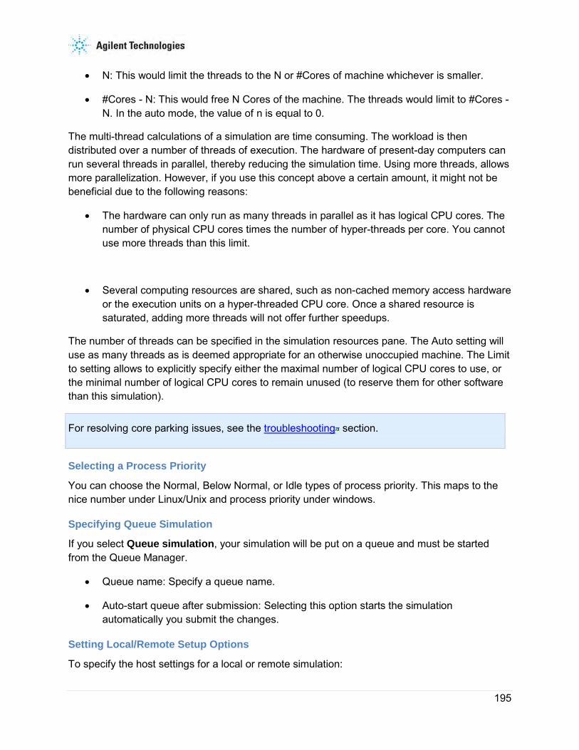
195
• N: This would limit the threads to the N or #Cores of machine whichever is smaller.
• #Cores - N: This would free N Cores of the machine. The threads would limit to #Cores - N. In the auto mode, the value of n is equal to 0.
The multi-thread calculations of a simulation are time consuming. The workload is then distributed over a number of threads of execution. The hardware of present-day computers can run several threads in parallel, thereby reducing the simulation time. Using more threads, allows more parallelization. However, if you use this concept above a certain amount, it might not be beneficial due to the following reasons:
• The hardware can only run as many threads in parallel as it has logical CPU cores. The number of physical CPU cores times the number of hyper-threads per core. You cannot use more threads than this limit.
• Several computing resources are shared, such as non-cached memory access hardware or the execution units on a hyper-threaded CPU core. Once a shared resource is saturated, adding more threads will not offer further speedups.
The number of threads can be specified in the simulation resources pane. The Auto setting will use as many threads as is deemed appropriate for an otherwise unoccupied machine. The Limit to setting allows to explicitly specify either the maximal number of logical CPU cores to use, or the minimal number of logical CPU cores to remain unused (to reserve them for other software than this simulation).
For resolving core parking issues, see the troubleshooting section.
Selecting a Process Priority
You can choose the Normal, Below Normal, or Idle types of process priority. This maps to the nice number under Linux/Unix and process priority under windows.
Specifying Queue Simulation
If you select Queue simulation, your simulation will be put on a queue and must be started from the Queue Manager.
• Queue name: Specify a queue name.
• Auto-start queue after submission: Selecting this option starts the simulation automatically you submit the changes.
Setting Local/Remote Setup Options
To specify the host settings for a local or remote simulation:
Electromagnetic
196
1. Choose EM > Simulation Setup to open the EM Setup window.
2. Select Resources in the left pane of the EM Setup window.
3. Select ADS (Local/Remote).
4. Specify the simulation directory.
5. Specify the number of threads.
6. Choose the process priority from the drop-down list.
7. Select Queue simulation to queue your simulation.
8. Provide a queue name.
9. If you want the queue to start automatically, select Auto-start queue after submission.
4.7.2 Setting up Third Party (Distributed) Simulation
If you want to use a third party workload management system, such as LSF, PBS Professional, and Sun Grid Engine, you can use the Distributed mode. In the distributed mode, you have access to the third party workload/queue management system to submit an EM simulation to a cluster of machines.
197
Before using the distributed mode, you need to set up a connection between your personal machine and the target machine that you want to use as submit host to the workload management system. The submit host is the one machine that will add and monitor simulation jobs given to the workload management system on behalf of your ADS session.
The submit host can be your local machine or can be a remote machine. To create this connection with the submit host you must first make the Job Manager aware of the workload management system on the submit host by adding the necessary configuration settings of the workload management system to the startup environment of the PVM deamon on the submit host.
On a Linux or a Solaris submit host add the necessary environment variables or source the required configuration script for your system into the PVM boot script ~/.eesofpvmprofile. On a Windows based submit host make sure the workload management system can be used by all users from a Windows command window. Refer to the documentation of your workload management environment for details on these configuration requirements. Next, ensure that the connection settings for the submit host are properly configured in the Job Manager Preferences.
Note For the distributed simulation with a third party workload management system where the local machine is a valid submit host, you do not need to define any formal PVM cluster configuration. A local PVM deamon will start and provide the submit and monitor capabilities with the workload management system.
To run simulations, the distributed mode assumes that the third party workload management system has been preconfigured to run ADS related tasks from the user command line environment on the submit host and on the execution hosts (the machines that will run the EM simulation) of the workload management system.
The distributed mode assumes that the third party workload management system has been preconfigured to run ADS related tasks from the command line environment. For setting up the third party workload management system refer to the documentation for your particular environment. You can find information for the supported workload management systems at the following location:
• LSF: http://www.platform.com
• PBS Professional: http://www.pbsgridworks.com/Default.aspx
• Sun Gridengine: http://gridengine.sunsource.net/
Make sure that the execution environment has the essential variables such as HPEESOF_DIR, PATH and ADS license settings are correctly defined on the hosts in the workload management system. For further details about the ADS configuration, refer to the ADS installation guide.
Electromagnetic
198
On Linux or Solaris machines, you can also add a ksh script .adsrc with the appropriate ADS environment settings inside your home directory on the cluster machines. The ~/.adsrc file is picked up by the simulation scripts just before a simulation starts.
Third Party (Distributed) Setup Options
In the EM Setup window, you can specify the following setup options for the distributed mode:
• The capability to start and stop the Job Manager: Click Start to initiate the Job Manager window and click Stop to close the Job Manager process. For more information, see Using the Job Manager.
• Specifying a submit host: Choose the required submit host (this can also be the local machine, as the submission host) for distributed simulation. Click Refresh to retrieve the list again.
• Specifying a submit queue: Choose the required submit queue on the selected submit host for distributed simulation. Click Refresh to retrieve the list again.
• Specifying parallel jobs for frequency sweep: Allows to specify the number of frequency points that will be calculated in parallel. It controls how the frequency sweep is distributed over the cluster. If it is equal to 1, it specifies a normal momentum simulation. If the value is greater than 1, you need a momentum turbo license and this is only supported between a cluster of Linux machines.
• Specifying a simulation directory: You need to define the remote simulation directory on the submit host for your distributed simulations. It sets the directory on the remote computer holding the EM files while the simulation is running. If the host mode is remote but the host is set to the local machine, the remote directory should be set to Shared local.
Note For the distributed simulation with a third party workload management system it is very important that this directory is visible to all cluster hosts in exactly the same way. Make sure mount points are identical.
• Specifying the number of threads: You can specify the number of threads used in the distributed simulation.

199
• Specifying process priority: You can choose the process priority among the Normal, Below Normal and Idle. This maps to the nice number on the Linux/Unix platform and process priority on the Windows platform.
• Specifying job control settings: You can specify the following job control settings:
o Submit user: Enables you to provide a user name if the local user name differs from that on the cluster.
o Email notification: Enables you to specify this option for notification purposes.
o Job name: Enables you to specify a name.
o Shell command at finish: Allows you to use shell commands.
o Resource String: Allows you to specify a resource string.
o Export env. Variables: Enables you to export environment variables.
• Specifying the start time: You can configure the simulation start time by selecting the required option from Start. You can choose either Now, At time, or After job(s) option.
• Specifying the termination time: You can configure the simulation expire time by selecting the required option from Expire. You can choose either Never or type the required time in the At/After text box.
Specifying Third Party (Distributed) Setup Options
To specify the distributed mode setup options:
1. Choose EM > Simulation Setup to open the EM Setup window.
2. Select Resources in the left pane of the EM Setup window.

Electromagnetic
200
3. Select the 3rd Party (distributed) option to specify the distributed setup options.
4. Specify the simulation directory.
5. Specify the number of threads.
6. Choose the process priority from the drop-down list.
7. Specify the job control settings.
8. Select the Start option.
9. Select the Expire option.
4.7.3 Using the Job Manager
The EM Setup window provides the capability to start and stop the Job Manager. For for more information, refer Using the Job Manager. The Job Manager is automatically started in mimimized mode when an EM Setup is being opened. Click the Start button to restart a closed Job Manager or to restore its main window, as shown in the following figure:
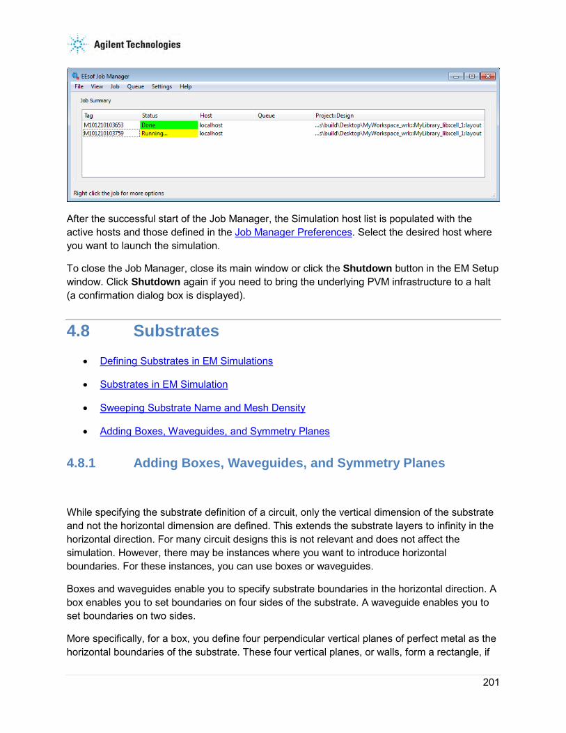
201
After the successful start of the Job Manager, the Simulation host list is populated with the active hosts and those defined in the Job Manager Preferences. Select the desired host where you want to launch the simulation.
To close the Job Manager, close its main window or click the Shutdown button in the EM Setup window. Click Shutdown again if you need to bring the underlying PVM infrastructure to a halt (a confirmation dialog box is displayed).
4.8 Substrates • Defining Substrates in EM Simulations
• Substrates in EM Simulation
• Sweeping Substrate Name and Mesh Density
• Adding Boxes, Waveguides, and Symmetry Planes
4.8.1 Adding Boxes, Waveguides, and Symmetry Planes
While specifying the substrate definition of a circuit, only the vertical dimension of the substrate and not the horizontal dimension are defined. This extends the substrate layers to infinity in the horizontal direction. For many circuit designs this is not relevant and does not affect the simulation. However, there may be instances where you want to introduce horizontal boundaries. For these instances, you can use boxes or waveguides.
Boxes and waveguides enable you to specify substrate boundaries in the horizontal direction. A box enables you to set boundaries on four sides of the substrate. A waveguide enables you to set boundaries on two sides.
More specifically, for a box, you define four perpendicular vertical planes of perfect metal as the horizontal boundaries of the substrate. These four vertical planes, or walls, form a rectangle, if

Electromagnetic
202
you are looking at the circuit from the top, along the z-axis. A box can be used only where the top and bottom layers in the substrate definition are groundplanes or impedance termination. Thus, the four vertical metal walls, plus the top and bottom groundplanes result in a box, hence the name (the walls are the sides, and the top and bottom ground planes are lid and base of the box).
A waveguide is similar, although for a waveguide you specify only two parallel walls. The substrate is therefore only bounded in the horizontal direction perpendicular to these walls. In the horizontal direction parallel to these walls, the substrate still extends to infinity. The top and bottom layers of the substrate must also be defined as groundplanes. The two sidewalls in combination and the top and bottom covers form a waveguide.
Adding a Box
A box defines the boundaries on four sides of the circuit substrate. Either one box or one waveguide can be applied to a circuit at a time. A box can be applied to a circuit only if the top and bottom layers of the substrate definition are defined as ground planes or impedance termination. The walls of the box are perfect metal. The ground planes can be defined either as perfect metals or a losse metal.
203
Adding a box to the circuit enables you to analyze the effects of enclosing the circuit in metal, for example, to identify box resonance. Box resonance can have a significant effect on S-parameters in a small band centered around the box resonance frequency. When a simulation is performed, the resonance frequencies will be noted in the status window when the circuit is simulated, along with the frequency bands where no smooth S-parameters can be calculated.
During a simulation, all current directions on the sidewalls of the box are taken into account.
Note Calibrated ports in the circuit (i.e., Single, Differential, Coplanar and Common mode ports) must be located on and perpendicular to the box edge, or an error will occur. Internal (uncalibrated) ports may be placed anywhere in the circuit and point in any direction.
To add a box:
1. Choose EM > Box-Waveguide > Add Box.
2. Position the mouse and click to define a corner of the box. Move the mouse to the diagonal corner and click once in the layout window.
You can also add a box by performing the following steps:
1. Choose EM > Box-Waveguide > Add Box.
2. From the Layout menu bar choose Insert > Coordinate Entry to open the Coordinate Entry dialog box.
3. Specify a value in the Coordinate Entry X and Coordinate Entry Y fields to specify a corner of the box.
4. Click Apply.
Editing a Box Once the box is applied, you cannot change its dimensions. If you want to change the size, you must delete the current box and add a new one.
Deleting a Box To delete a box, choose EM > Box-Waveguide > Delete Box.

Electromagnetic
204
Viewing Layout Layer Settings of a Box The box is defined as a layout layer named momentum_box. You may review the layout layer settings, but it is a protected layer, so you should not change the settings of this layer. To view the box layer specifications:
1. Choose Options > Layers.
2. Select momentum_box from the Layers list. The layer settings are displayed. For more information on these parameters, refer to Schematic Capture and Layout.
Adding a Waveguide
A waveguide defines the boundaries on two, parallel sides of the circuit substrate. Either one box or one waveguide can be applied to a circuit at a time. A waveguide can be applied to a circuit only if the top and bottom layers of the substrate definition are defined as ground planes or impedance termination. The walls of the waveguide are perfect metal. The ground planes can be defined either as perfect metals or metal with loss.
During a simulation, all current directions on the sidewalls of the waveguide are taken into account. To add a waveguide:
1. Choose EM > Box-Waveguide > Add Waveguide. This opens the Add Waveguide message window, as shown in the following figure:
2. Select the direction of the waveguide. To insert the waveguide parallel to the x-axis, click X-axis. To insert the waveguide parallel to the y-axis, click Y-axis.
3. Position the mouse and click to define one wall of the waveguide. Move the mouse to the position of a point on the second wall and click once in the layout window.
You can also add a waveguide by performing the following steps:
1. Choose EM > Box-Waveguide > Add Waveguide.
2. Select the direction of the waveguide. To insert the waveguide parallel to the x-axis, click X-axis. To insert the waveguide parallel to the y-axis, click Y-axis.
3. Choose Insert > Coordinate Entry in the layout.

205
4. Specify a value for the Coordinate Entry X and Coordinate Entry Y fields to specify a point on the edge of the substrate.
5. Click Apply.
6. Enter the coordinates of a point on the second, parallel edge of the substrate and click Apply.
These boundaries specify the edges of the substrate and the width of the waveguide.
Editing a Waveguide Once the waveguide is applied, you cannot change its dimensions. If you want to change the size, you must delete the current waveguide and add a new one.
Deleting a Waveguide To delete a waveguide,
1. Select EM > Box-Waveguide > Delete Waveguide.
2. Click Yes in the message window to remove the waveguide from the layout.
Viewing Layout Layer Settings of a Waveguide The waveguide is defined as a layout layer named momentum_box. You may review the layout layer settings, but it is a protected layer, so you should not change the settings of this layer.
To view the waveguide layer specifications:
1. Choose Options > Layers.
2. Select momentum_box from the Layers list. The layer settings are displayed. For more information on these parameters, refer to Schematic Capture and Layout.
About Boxes and Waveguides
You may need to simulate a circuit in a box or waveguide in the following situations:
• The actual circuit is enclosed in a metal box: Circuits are often encased in metal enclosures. By adding a box to your design, the metal sidewalls that are present in the real structure may be included in the simulation. This is useful is you suspect that the presence of these sidewalls will have an immediate effect on the behavior of the circuit. For example, "broad-coupled filters" are placed in metal enclosures (a box) and the sidewalls can have an significant influence on the filter characteristics.

Electromagnetic
206
• The nearby metal sidewalls may affect circuit performance: You may want to use a box or waveguide because metal sidewalls are present in the real structure and there may be an effect from these sidewalls on the characteristics of the circuit. This can be a parasitic, unwanted effect. If the effects of the sidewalls were not taken into account while designing the circuit, you can verify any effect that the sidewalls may have on your circuit. In most cases, when the sidewalls are not too close to the actual circuit, the effect of the sidewalls on the simulation results will be marginal. There is, however a specific, significant condition, which is unique for structures with sidewalls.
• The box may resonate: A resonating box is a physical effect where, under the condition of certain frequency and box size combination, the box actually starts resonating at a certain frequency. Because a box resonance has a significant effect on S-parameters in a (small) band centered around the box resonance frequency which cannot be represented by a smooth function, no smooth adaptive S-parameters will be available in this frequency band. When simulating such a circuit, Momentum will inform you of these box resonance frequencies, of the frequency bands where there will not be smooth S-parameters available and of the quality factor (a measure for the sharpness of the box resonance, depending on the losses). In the case of waveguide, the effect is the excitation of a waveguide mode. If your circuit will be positioned near sidewalls, you may want to add a waveguide to determine whether they have an effect on the performance of the circuit.
• The propagating modes may be present: You may have a situation where there are no metal sidewalls in the structure, but the substrate definition is bounded by other material (for example, you have a finite-size substrate where the dielectric material abruptly ends, so you have a dielectric-air transition). Although Momentum boxes and waveguides are defined as perfect metals and not dielectric material, you may decide that defining a metallic enclosure in the simulated circuit may be more representative of the real structure than using no enclosure.
Adding Absorbing Layers under a Cover You may want to model your box or waveguide as having absorbing layers between the covers and the layout. You can use a substrate interface layer, define its thickness, and its absorbing properties using ε and µ (make sure that ε and µ are accurate specifications for this layer). Adding absorbing layers to a box would have an effect on any box resonances that would occur by producing a weaker resonance, that is, the quality factor of the box resonances would lower significantly.

207
Boxes, Waveguides, and Radiation Patterns If you have a structure enclosed in a box or waveguide and you want to calculate radiation patterns for it after the simulation, you need to set the top and bottom planes to values between 376 and 378. There are also other considerations.
Adding a Symmetry Plane
A symmetry plane defines the boundary on one side of the circuit substrate. Only one box, or one waveguide, or one symmetry plane can be applied to a circuit at a time. When a symmetry plane is defined, the simulation results will be equivalent to the results of a larger circuit that would be created by mirroring the circuit about the symmetry plane. For symmetric circuits, this enables faster simulations that require less memory because only half the actual structure needs to be simulated.
To add a symmetry plane:
1. Choose EM > FEM Symmetry Plane > Add Symmetry Plane.
2. Select the direction of the symmetry plane. To insert the symmetry plane parallel to the x-axis, click X-axis. To insert the symmetry plane parallel to the y-axis, click Y-axis.
3. Insert the symmetry plane using one of the following two methods:
o Position the mouse and click to define the location of the symmetry plane.
o From the Layout menu bar choose Insert > Coordinate Entry and use the Coordinate Entry X and Coordinate Entry Y fields to specify a point on the edge of the substrate.
4. Click Apply.
This boundary specifies the edge of the substrate where the plane of symmetry will be applied.
A symmetry plane is not supported by Momentum simulations.
Editing a Symmetry Plane Once the symmetry plane is applied, you cannot change its location. If you want to change the location or orientation, you must delete the current symmetry plane and add a new one.
Deleting a Symmetry Plane To delete a symmetry plane:
1. Choose EM > FEM Symmetry Plane> Delete Symmetry Plane. The symmetry plane is removed from the layout.

Electromagnetic
208
4.8.2 Substrates in EM Simulation
A substrate in EM simulation describes the media where a circuit exists. An example is the substrate of a multilayer circuit board, which consists of layers of metal traces, insulating material, ground planes, vias that connect traces, and air that surrounds the board. A substrate definition enables you to specify properties, such as, the number of layers in the substrate, the dielectric constant, and the height of each layer for your circuit.
A substrate consists of the following types of alternating items:
• Substrate Layer: This layer defines the dielectric media, ground planes, covers, air, or other layered material.
• Interface Layer: This is the conductive layer in between the substrate layers, which is used in conjunction with the layout layers. By mapping layout layers to interface layers, you can position the layout layers that your circuit is drawn on within the substrate.
The top and bottom of the substrate either end with a Cover (Interface) or an infinitely thick Substrate Layer. For more information, see Defining Substrates in an EM Simulation
This section provides information about creating, modifying, and editing a substrate.
Substrate Editor
You can open the Substrate Editor window in the following ways:
• From the ADS Main Window, choose File > New > Substrate and click OK.
• From the ADS Main Window, select Library View tab. Right-click any library or cell and choose New Substrate.

209
• From the Layout Window, choose EM > Substrate.
The key components of substrate editor are listed below:
1. Main Menu bar: Contains menu options to edit or create a new substrate.
2. Toolbar: Contains the most commonly used buttons.
3. Substrate view: Displays 3D cross-section view of substrate stack with mask mappings, it has basic operations to edit the substrate definition.
4. Status bar: Notifies about warnings or errors for the substrate.
5. Properties panel: This panel, on the right, allows editing the properties of the currently selected item of the substrate.
Creating a Substrate
To create a new substrate:
1. Choose File > New from the Substrate window or File > New > Substrate from the ADS Main window.
2. From the New Substrate window, select the library where you want to create the substrate.
3. Type the substrate name in File Name and click OK.
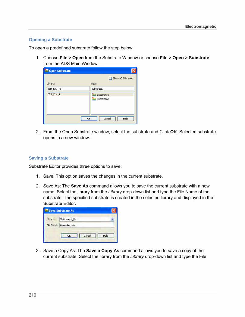
Electromagnetic
210
Opening a Substrate
To open a predefined substrate follow the step below:
1. Choose File > Open from the Substrate Window or choose File > Open > Substrate from the ADS Main Window.
2. From the Open Substrate window, select the substrate and Click OK. Selected substrate opens in a new window.
Saving a Substrate
Substrate Editor provides three options to save:
1. Save: This option saves the changes in the current substrate.
2. Save As: The Save As command allows you to save the current substrate with a new name. Select the library from the Library drop-down list and type the File Name of the substrate. The specified substrate is created in the selected library and displayed in the Substrate Editor.
3. Save a Copy As: The Save a Copy As command allows you to save a copy of the current substrate. Select the library from the Library drop-down list and type the File

211
Name of the substrate. A copy of the current substrate is created in the specified library.
Inserting, Moving, and Deleting Items
The Substrate View enables you to visualize the substrate stack and do basic editing. To add or delete an item in the substrate, right-click in the substrate view and select from the list of option displayed in the pop-up menu. After selecting the desired action, the properties associated with it are displayed in the right panel of the Substrate Editor.
Context menus Right-click on a Substrate Layer and you may see some of the following menus depending on the interface position and properties:
• Insert Substrate Layer Above - Inserts a new substrate layer with an interface layer above the selected layer.
• Insert Substrate Layer Below - inserts a new substrate layer with an interface layer below the selected layer.
• Delete with Upper Layer - Deletes the substrate layer above the selected layer.
• Delete with Lower Layer - Deletes the substrate layer below the selected layer.
• Map Conductor Via - Inserts a new conductor via in the selected substrate.
• Map Semiconductor Via - Inserts a new semiconductor via in the selected substrate.
• Map Dielectric Via - Inserts a new dielectric via in the selected layer.
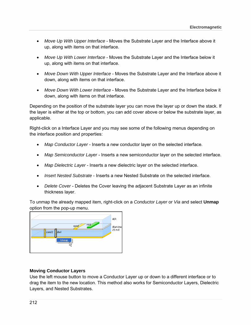
Electromagnetic
212
• Move Up With Upper Interface - Moves the Substrate Layer and the Interface above it up, along with items on that interface.
• Move Up With Lower Interface - Moves the Substrate Layer and the Interface below it up, along with items on that interface.
• Move Down With Upper Interface - Moves the Substrate Layer and the Interface above it down, along with items on that interface.
• Move Down With Lower Interface - Moves the Substrate Layer and the Interface below it down, along with items on that interface.
Depending on the position of the substrate layer you can move the layer up or down the stack. If the layer is either at the top or bottom, you can add cover above or below the substrate layer, as applicable.
Right-click on a Interface Layer and you may see some of the following menus depending on the interface position and properties:
• Map Conductor Layer - Inserts a new conductor layer on the selected interface.
• Map Semiconductor Layer - Inserts a new semiconductor layer on the selected interface.
• Map Dielectric Layer - Inserts a new dielectric layer on the selected interface.
• Insert Nested Substrate - Inserts a new Nested Substrate on the selected interface.
• Delete Cover - Deletes the Cover leaving the adjacent Substrate Layer as an infinite thickness layer.
To unmap the already mapped item, right-click on a Conductor Layer or Via and select Unmap option from the pop-up menu.
Moving Conductor Layers Use the left mouse button to move a Conductor Layer up or down to a different interface or to drag the item to the new location. This method also works for Semiconductor Layers, Dielectric Layers, and Nested Substrates.
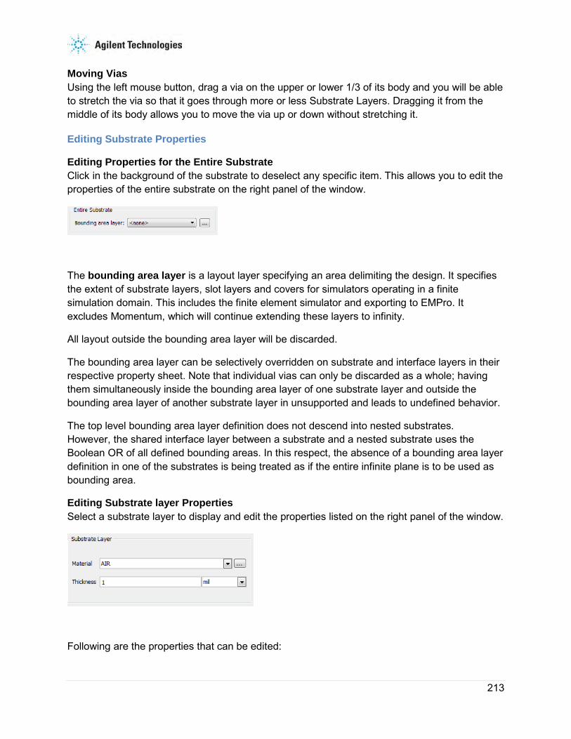
213
Moving Vias Using the left mouse button, drag a via on the upper or lower 1/3 of its body and you will be able to stretch the via so that it goes through more or less Substrate Layers. Dragging it from the middle of its body allows you to move the via up or down without stretching it.
Editing Substrate Properties
Editing Properties for the Entire Substrate Click in the background of the substrate to deselect any specific item. This allows you to edit the properties of the entire substrate on the right panel of the window.
The bounding area layer is a layout layer specifying an area delimiting the design. It specifies the extent of substrate layers, slot layers and covers for simulators operating in a finite simulation domain. This includes the finite element simulator and exporting to EMPro. It excludes Momentum, which will continue extending these layers to infinity.
All layout outside the bounding area layer will be discarded.
The bounding area layer can be selectively overridden on substrate and interface layers in their respective property sheet. Note that individual vias can only be discarded as a whole; having them simultaneously inside the bounding area layer of one substrate layer and outside the bounding area layer of another substrate layer in unsupported and leads to undefined behavior.
The top level bounding area layer definition does not descend into nested substrates. However, the shared interface layer between a substrate and a nested substrate uses the Boolean OR of all defined bounding areas. In this respect, the absence of a bounding area layer definition in one of the substrates is being treated as if the entire infinite plane is to be used as bounding area.
Editing Substrate layer Properties Select a substrate layer to display and edit the properties listed on the right panel of the window.
Following are the properties that can be edited:

Electromagnetic
214
• Material - This property allows you to select the layer material from the Material drop-down list. Materials are defined in the Materials Definition dialog box. Click the button to open the Material Definition dialog box where you can define a new material. The defined material is added automatically in the Material drop-down list.
• Thickness - This property allows you to define the thickness of the layer. The units can be selected from the Thickness drop-down list.
Editing Interface Layer Properties Select an Interface layer to define the interface layer as one of the following:
• Cover - This option is only available for the top or bottom Interface. If it is enabled, the following properties can also be set:
o 377 Ohm Termination - Check the box to enable this termination. If this option is checked, you cannot specify Material and Thickness.
o Material - This property allows you to select the layer material from the Material drop-down list. Materials are defined in the Materials Definition dialog box. Click the button to open the Material Definition dialog box where you can define a new material. The defined material is added automatically in the Material drop-down list.
o Thickness - This property allows you to define the thickness of the layer. The units can be selected from the Thickness drop-down list.
• Strip Plane - Allows the mapping of Conductor, Semiconductor, and Dielectric Layers, and the insertion of Nested Substrates.
• Slot Plane - Allows the mapping of Slot Layers.
Editing Conductor Layer Properties Select a Conductor layer to define any of the following properties:

215
• Layer - Allows you to map the mask layer with layout layer from the Layer drop-down list. To add new layout layer click the button (next to Layer drop-down list).
• Only pins and pin shapes from layer - Allows you to only map the pins and pin shapes into the substrate, but not the geometry.
• Material - Defines material property for the mask layer from the Material drop-down list. To add new material layer click the button (next to Material drop-down list).
• Operation - The operation transforms 2D shapes drawn on a mask into 3D objects. For example, select the proper expand operation to define the thickness of a conductor mask.
• Position - Defines the position of the layer.
• Thickness - Defines the thickness of the layer.
• Surface roughness model - Allows you to select Surface roughness model at Top and Bottom.
• Precedence - Precedence specifies the precedence of a layout layer over another layer, if two or more layout layers are assigned to the same interface or substrate layer and objects overlap. Precedence is used by the mesh maker so that objects on the layer with the greatest precedence number are meshed and any overlap with objects on layers with lesser numbers are logically subtracted from the circuit. If you do not set the precedence, and there are overlapping objects, a mesh will automatically and arbitrarily be created, with no errors reported.
Editing Via Properties Select a Conductor Via layer to edit any of the following properties:

Electromagnetic
216
• Layer - Allows you to map the mask layer with layout layer from the Layer drop-down list. To add new layout layer click the button (next to Layer drop-down list).
• Material - Defines material property for the mask layer from the Material drop-down list. To add new material layer click the button (next to Material drop-down list).
• Surface roughness model - Allows you to select Surface roughness model for the sides of the via.
• Precedence - Precedence specifies which layout layer has precedence over another if two or more layout layers are assigned.
Editing Nested Substrate Properties Select a Nested Substrate to edit any of the following properties:
• Use a nested technology - Check this if your nested substrate represents a substrate from a different technology. With this un-checked you may nest two substrates from the current technology.

217
• Nested Technology - Choose a Nested Technology from the Nested Technology drop-down list. The chosen Nested Technology determines if the substrate appears flipped or not. Click the button to create or edit Nested Technologies.
• Nested Library - This is the name of the library specified in the chosen Nested Technology. This is not editable.
• Flipped - The shows if the nested technology is flipped. This is not editable.
• Nested Substrate - Choose a Substrate from the Nested Library to specify the EM properties of the layouts that will be placed on layouts using this substrate.
• Alignment within nested substrate - This chooses a location within the nested substrate that will be aligned with the interface of the current substrate. Choosing the Bottom interface of the nested substrate places the nested substrate on top of the current substrate interface. Choosing the Top interface of the nested substrate places the nested substrate on bottom of the current substrate interface. You may also choose a strip, slot, or via layer of the nested substrate that will be aligned with the current substrate interface. The Bottom or Top choice in the combobox is used to choose the bottom or top of the strip or via layer that was selected.
• Offset - This allows you to move your Nested Substrate up or down relative to the interface it is on.
• Precedence increase - Precedence specifies which substrate has precedence over another if two or more substrates are at the same location. The substrate with the higher precedence occupies the overlapped area.
See Nested Technology and Setting up Multi-Technology Designs for more information about using Nested Technologies and Nested Substrates.
Verifying Substrate Definition
After creating the substrate definition, choose File > Check (from the Substrate Editor window) to verify the created substrate definition. The verification result or errors (if any) are displayed in the Check Substrate message window.
Setting a Default Substrate
A default substrate can be specified for each library. This substrate can be any substrate in the library or from any library referenced by the technology of the library. A default substrate will be the initial value of the substrate name when any new emSetup views are created. A design kit can have a default substrate and any other libraries that uses the design kit technology will inherit the default substrate from the design kit.

Electromagnetic
218
The Set Default Substrate dialog can be opened from the Options > Set Default Substrate menu on the Substrate Window. It can also be open from the Set Default Substrate context menu on substrates in the ADS Main window.
The Library combobox specifies which library the default substrate is for. The Default Substrate combobox specifies the default substrate. The substrate choices include those in the specified library and any libraries referenced by the technology of the specified library. It also includes the choice to Inherit from referenced libraries. If this is chosen, the referenced libraries are searched for a default substrate specification and the first found will become the default substrate.
Importing a Substrate
To import a substrate choose File > Import from the Substrate editor window or the ADS Main window. The following import options are available:
• SLM Substrate File
• ltd Substrate File
• Substrate From Database
• Substrate From Schematic
SLM Substrate File To import substrate from a slm file, choose SLM Substrate file.

219
ltd Substrate File To import substrate from an ltd file, choose ltd Substrate file.
Substrate From Database To import substrate from a database, choose Substrate From Database.
Substrate From Schematic To import a substrate from a schematic, choose Substrate From Schematic.

Electromagnetic
220
4.8.3 Sweeping Substrate Name and Mesh Density
To support sweeps over a substrate name, you can add a cell parameter, Substrate, of the string type. Use the Substrate Editor to define and save different substrate setups to sweep through. Add a custom parameter to the design called Substrate by performing the following steps:
1. In the layout window, select File > Design Parameters.
2. Click the Cell Parameters tab.
3. Add a parameter named Substrate, of type String, with a Default Value set to an existing substrate, using the "<libraryName>:<substrateName>" format. Double quotes are also included.
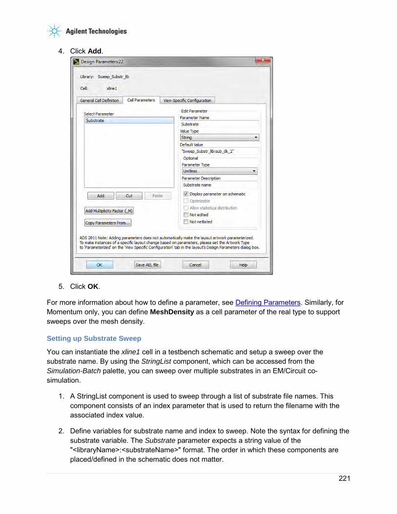
221
4. Click Add.
5. Click OK.
For more information about how to define a parameter, see Defining Parameters. Similarly, for Momentum only, you can define MeshDensity as a cell parameter of the real type to support sweeps over the mesh density.
Setting up Substrate Sweep
You can instantiate the xline1 cell in a testbench schematic and setup a sweep over the substrate name. By using the StringList component, which can be accessed from the Simulation-Batch palette, you can sweep over multiple substrates in an EM/Circuit co-simulation.
1. A StringList component is used to sweep through a list of substrate file names. This component consists of an index parameter that is used to return the filename with the associated index value.
2. Define variables for substrate name and index to sweep. Note the syntax for defining the substrate variable. The Substrate parameter expects a string value of the "<libraryName>:<substrateName>" format. The order in which these components are placed/defined in the schematic does not matter.
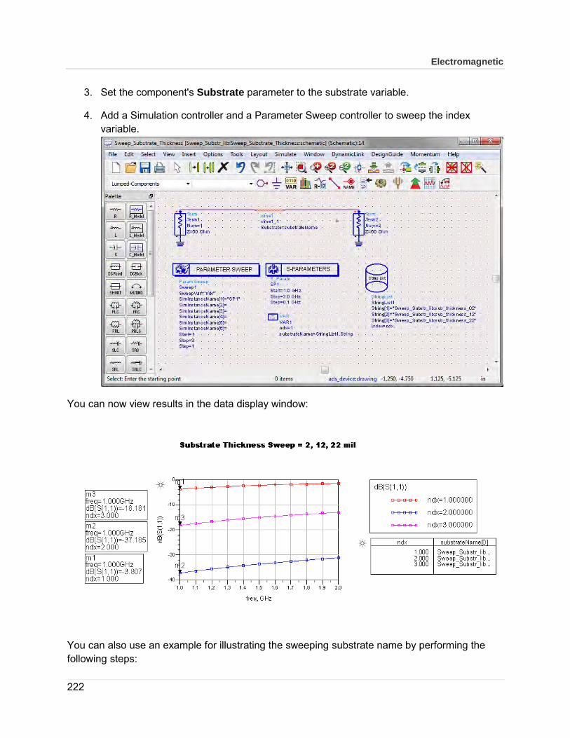
Electromagnetic
222
3. Set the component's Substrate parameter to the substrate variable.
4. Add a Simulation controller and a Parameter Sweep controller to sweep the index variable.
You can now view results in the data display window:
You can also use an example for illustrating the sweeping substrate name by performing the following steps:
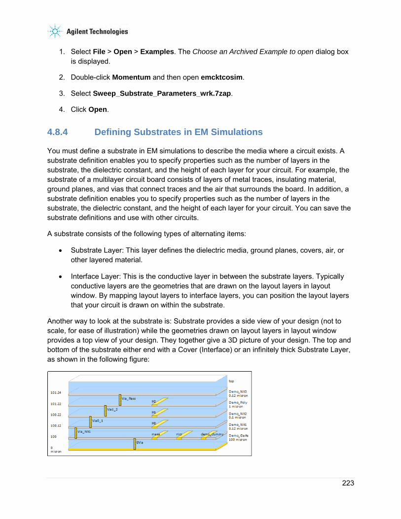
223
1. Select File > Open > Examples. The Choose an Archived Example to open dialog box is displayed.
2. Double-click Momentum and then open emcktcosim.
3. Select Sweep_Substrate_Parameters_wrk.7zap.
4. Click Open.
4.8.4 Defining Substrates in EM Simulations
You must define a substrate in EM simulations to describe the media where a circuit exists. A substrate definition enables you to specify properties such as the number of layers in the substrate, the dielectric constant, and the height of each layer for your circuit. For example, the substrate of a multilayer circuit board consists of layers of metal traces, insulating material, ground planes, and vias that connect traces and the air that surrounds the board. In addition, a substrate definition enables you to specify properties such as the number of layers in the substrate, the dielectric constant, and the height of each layer for your circuit. You can save the substrate definitions and use with other circuits.
A substrate consists of the following types of alternating items:
• Substrate Layer: This layer defines the dielectric media, ground planes, covers, air, or other layered material.
• Interface Layer: This is the conductive layer in between the substrate layers. Typically conductive layers are the geometries that are drawn on the layout layers in layout window. By mapping layout layers to interface layers, you can position the layout layers that your circuit is drawn on within the substrate.
Another way to look at the substrate is: Substrate provides a side view of your design (not to scale, for ease of illustration) while the geometries drawn on layout layers in layout window provides a top view of your design. They together give a 3D picture of your design. The top and bottom of the substrate either end with a Cover (Interface) or an infinitely thick Substrate Layer, as shown in the following figure:

Electromagnetic
224
Opening the Substrate Editor
You can open the Substrate Editor window in the following ways:
• From the ADS Main window, choose File > New > Substrate and click OK.
• From the ADS Main window, select Library View tab. Right-click any library or cell and choose New Substrate.
• From the Layout window, choose EM > Substrate.
• From the EM Setup window, select Substrate in the left pane. Then, click New.
The Substrate Editor window is displayed, as shown in the following figure:
Selecting a Predefined Substrate
To open a predefined substrate:
1. Select EM > Simulation Setup to open the EM Setup window.
2. Select Substrate.
3. Select an existing ADS substrate file from the drop-down list.
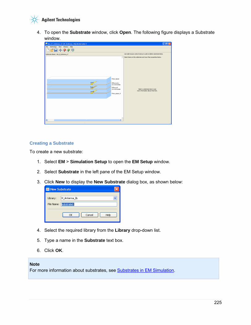
225
4. To open the Substrate window, click Open. The following figure displays a Substrate window.
Creating a Substrate
To create a new substrate:
1. Select EM > Simulation Setup to open the EM Setup window.
2. Select Substrate in the left pane of the EM Setup window.
3. Click New to display the New Substrate dialog box, as shown below:
4. Select the required library from the Library drop-down list.
5. Type a name in the Substrate text box.
6. Click OK.
Note For more information about substrates, see Substrates in EM Simulation.

Electromagnetic
226
Adding, Moving, and Deleting Layers
To organize your substrate layers in the correct order, you can delete, add, and move layers.
To add a substrate layer:
1. Right-click a substrate layer in the Substrate Name list that has the same basic property (open boundary, closed boundary, or finite thickness) as the layer you are adding.
2. Click Insert Substrate Layer Above or Insert Substrate Layer Below to add a new layer.
To move a substrate layer:
1. Right-click a substrate layer that you want to move in the Substrate Name list.
2. Select one of the following options:
o Move Up With Upper Interface
o Move Up With Lower Interface
o Move Down With Upper Interface
o Move Down With Lower Interface
To delete a substrate layer:
1. Right-click a substrate layer.
2. Select Delete with Upper Layer or Delete with Lower Layer to delete a layer definition.
Modifying Substrate Layers
After adding a substrate layer, you can set the properties in the right panel of the Substrate Editor window.
Defining Material While editing a material associated with a substrate layer, you can specify the permittivity and permeability (MUr) properties. The real portion of the relative permittivity, , is a dimensionless
quantity and is identical to the material relative dielectric constant, . To represent a dielectric that dissipates the power of a high-frequency electric field, enter the dielectric loss tangent,
, of the material in the Loss Tangent field. The smaller the loss tangent, the less lossy the material. The real portion of the relative permeability, , is a dimensionless quantity and is identical to the material's relative permeability constant. To represent a dielectric that dissipates the power of a high-frequency magnetic field, enter the magnetic loss tangent, , of the
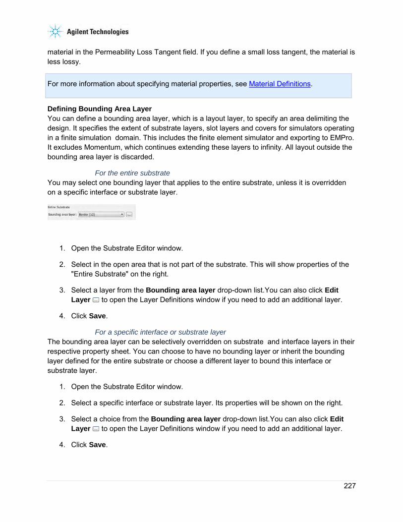
227
material in the Permeability Loss Tangent field. If you define a small loss tangent, the material is less lossy.
For more information about specifying material properties, see Material Definitions.
Defining Bounding Area Layer You can define a bounding area layer, which is a layout layer, to specify an area delimiting the design. It specifies the extent of substrate layers, slot layers and covers for simulators operating in a finite simulation domain. This includes the finite element simulator and exporting to EMPro. It excludes Momentum, which continues extending these layers to infinity. All layout outside the bounding area layer is discarded.
For the entire substrate You may select one bounding layer that applies to the entire substrate, unless it is overridden on a specific interface or substrate layer.
1. Open the Substrate Editor window.
2. Select in the open area that is not part of the substrate. This will show properties of the "Entire Substrate" on the right.
3. Select a layer from the Bounding area layer drop-down list.You can also click Edit Layer to open the Layer Definitions window if you need to add an additional layer.
4. Click Save.
For a specific interface or substrate layer The bounding area layer can be selectively overridden on substrate and interface layers in their respective property sheet. You can choose to have no bounding layer or inherit the bounding layer defined for the entire substrate or choose a different layer to bound this interface or substrate layer.
1. Open the Substrate Editor window.
2. Select a specific interface or substrate layer. Its properties will be shown on the right.
3. Select a choice from the Bounding area layer drop-down list.You can also click Edit Layer to open the Layer Definitions window if you need to add an additional layer.
4. Click Save.

Electromagnetic
228
After adding a bounding layers the substrate will appear to be cut on the right edge and will display the name of the layer that bounds each interface and substrate layer.
Note that individual vias can only be discarded as a whole; having them simultaneously inside the bounding area layer of one substrate layer and outside the bounding area layer of another substrate layer is unsupported and leads to undefined behavior.
The top level bounding area layer definition does not descend into nested substrates. However, the shared interface layer between a substrate and a nested substrate uses the Boolean OR of all defined bounding areas. In this respect, the absence of a bounding area layer definition in one of the substrates is being treated as if the entire infinite plane is used as a bounding area.
Bounding Area Layer applies only to FEM simulations.
Modifying Interface Layers
To identify the areas of a layout layer that are conductive, you can specify a layer as follows:
• Strip: A Strip defines the objects on the layout layer as conductive, the area surrounding the objects is not, as shown in the following figure:
• Slot: A Slot is the inverse of a strip, it defines the objects on the layout layer as not conductive, but the area of this layer surrounding the objects is conductive. When

229
simulated, Momentum and FEM considers the electric field distribution (the equivalent magnetic current flow) in the slot.
Note Conductivity in slot metallization is ignored and perfect metallization is assumed.
• Cover: A cover available only for the top or bottom Interface. If it is enabled, you can also set the following properties:
o 377 Ohm Termination - Select this option to enable this termination. If this option is selected, you cannot specify Material and Thickness.
o Material - This property allows you to select the layer material from the Material drop-down list. Materials are defined in the Materials Definition dialog box. Click the button to open the Material Definition dialog box where you can define a new material. The defined material is added automatically in the Material drop-down list.
o Thickness - This property allows you to define the thickness of the layer. You can also select the units for thickness.
Some examples of using strips and slots include:
• The patches of the Double_Patch antenna example. They are drawn on the layout layer named top_met, and are conductive. This layout layer is mapped to a metallization layer that is defined as a strip.
• The slots of the Slot_dipole antenna example. The slots are drawn on the layout layer named slot. The slots are not conductive, but the area surrounding the slots is. This layout layer is mapped to a metallization layer that is defined as a slot.
Note that a layout can have many other layers that are not part of the actual circuit, such as text or error reporting layers. For the purposes of an Momentum simulation, they are ignored. If layout layers containing parts of the circuit are not mapped to metallization layers, they are ignored as well.

Electromagnetic
230
Mapping a Layout Layer
Layout layers that contain any shapes or components that are part of the circuit must be mapped to metallization layers. If layout layers are not mapped to metallization layers, they are not included in the simulation.
To map a layout layer:
1. Open the Substrate Editor window.
2. Select an interface layer.
3. Select the Strip Plane or Slot Plane option.
4. To map the layer as a via, right-click the substrate layer that you want the via to cut through.
5. Select either Map Conductor Via, Map Semiconductor Via, or Map Dielectric Via.
After mapping vias, it is recommended to convert the vias to rectangles or square vias in the layout design to reduce memory consumption.
6. To define the conductivity characteristics of this layer, see Defining Conductor Layer Properties.
7. If you have overlapping layers, you need to set overlap precedence. For more information, see Setting Overlap Precedence.
8. Click Save.
Unmapping a Layer If you want to change the location of a layer or remove one from the substrate definition, use Unmap.
To unmap a layer:
1. Open the Substrate Editor window.
2. Select a mapped layout layer from the Layers list.
3. Right-click a substrate layer or the interface where the layout layer is mapped.
4. Click Unmap. A message box appears.
5. Click OK. This removes all layout layers assigned to this position.
6. To remap a layer, refer to the steps in Mapping a Layout Layer.
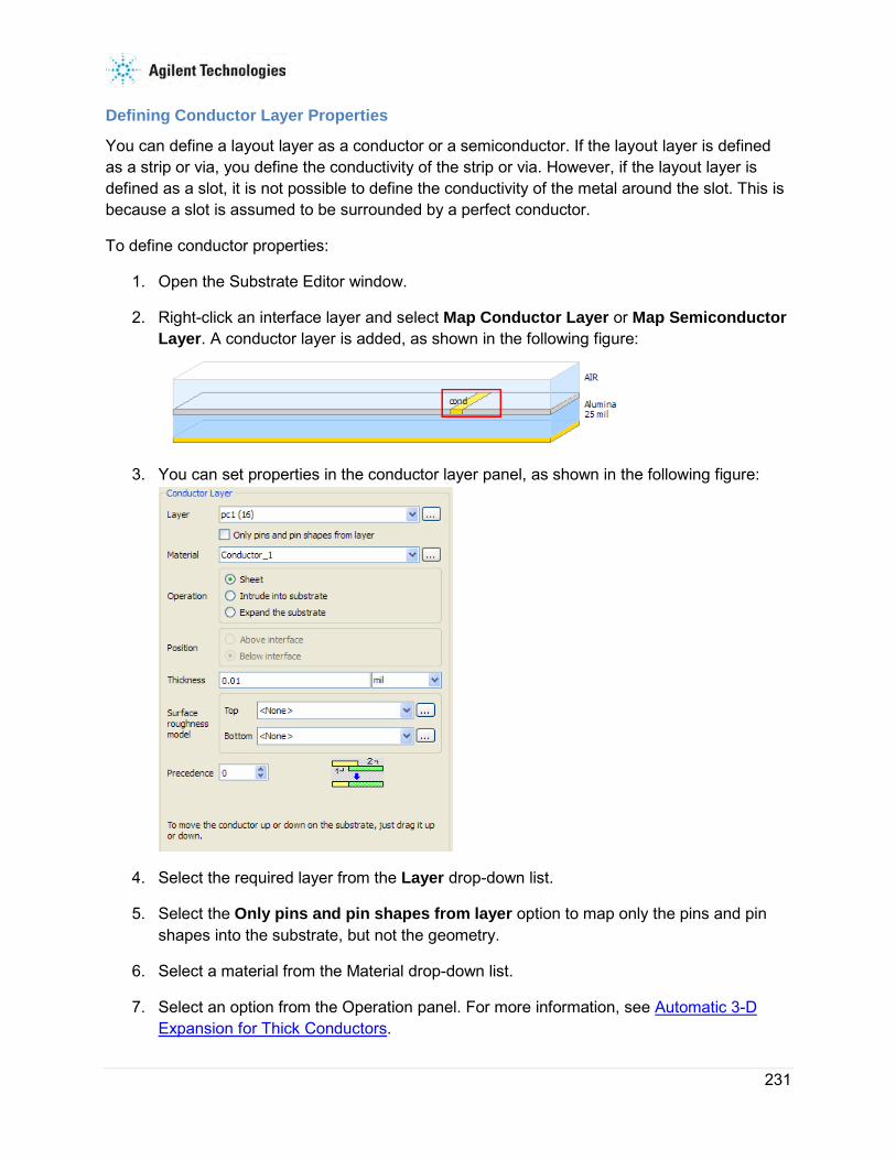
231
Defining Conductor Layer Properties
You can define a layout layer as a conductor or a semiconductor. If the layout layer is defined as a strip or via, you define the conductivity of the strip or via. However, if the layout layer is defined as a slot, it is not possible to define the conductivity of the metal around the slot. This is because a slot is assumed to be surrounded by a perfect conductor.
To define conductor properties:
1. Open the Substrate Editor window.
2. Right-click an interface layer and select Map Conductor Layer or Map Semiconductor Layer. A conductor layer is added, as shown in the following figure:
3. You can set properties in the conductor layer panel, as shown in the following figure:
4. Select the required layer from the Layer drop-down list.
5. Select the Only pins and pin shapes from layer option to map only the pins and pin shapes into the substrate, but not the geometry.
6. Select a material from the Material drop-down list.
7. Select an option from the Operation panel. For more information, see Automatic 3-D Expansion for Thick Conductors.

Electromagnetic
232
8. Type the conductor thickness in the Thickness text box and select a unit.
9. Specify the surface roughness model.
10. Set overlap precedence. For more information, see Setting Overlap Precedence.
11. Repeat these steps for the remaining mapped layout layers.
12. Click Save.
Automatic 3-D Expansion for Thick Conductors Conductors with finite thickness can be modeled using the 3D metal expansion feature. This feature automatically expands the mask of a conductor with finite thickness in the direction orthogonal to the layered medium, using the specified thickness of this conductor.
3D expansion is activated by selecting either the Intrude into Substrate or Expand the Substrate option. In both cases, an extra dielectric layer is included in the internal substrate model. This is done for each metal layer that is expanded. The thickness values of the dielectric layers in between the metal layers are not changed, which preserves the capacitance value between two conductors lying on top of each other in the substrates.
To select the automated 3-D Metal Expansion Substrate items:
1. Open the Substrate Editor window.
2. Select the cond layer.
3. In the Conductor Layer panel, select the substrate layer or the interface where the layout layer is mapped.
4. Choose either Intrude into Substrate or Expand the Substrate.
5. Select the required position: Above Interface or Below Interface.
Simulations with automatic expansion require more simulation time and memory, but result in more accurate simulation results. Typically, when the width/thickness aspect ratio is smaller than a factor of 5, the effect of accounting for the finite thickness of the conductors need to be allowed in Momentum simulations.
Consider an example, where an extra dielectric layer is inserted (indicated with [new] in the figure), which in the case of an above interface expansion has the dielectric properties of the layer above the metal layer. In the case of a below interface expansion, the new layer has the

233
material properties of the layer below the metal layer. The following figure illustrates the internal substrate model when using the Expand the Substrate option and selecting the Above Interface expansion for a conductor.
The following figure illustrates the internal substrate model when using the Expand the Substrate option and selecting the Below Interface expansion for a conductor.
If you select Intrude into Substrate, the above expansion is illustrated in the following figure:
Note Extra internal metallization layers are automatically added in Momentum and FEM to model the currents on all four sides of the finite thickness conductor.
Setting Overlap Precedence Overlap precedence specifies which layout layer has precedence over another if two or more layout layers are assigned to the same metallization layer and objects on the metallization layer overlap. Precedence is used by the mesh maker so that objects on the layer with the greatest precedence number are meshed and any overlap with objects on layers with lesser numbers is
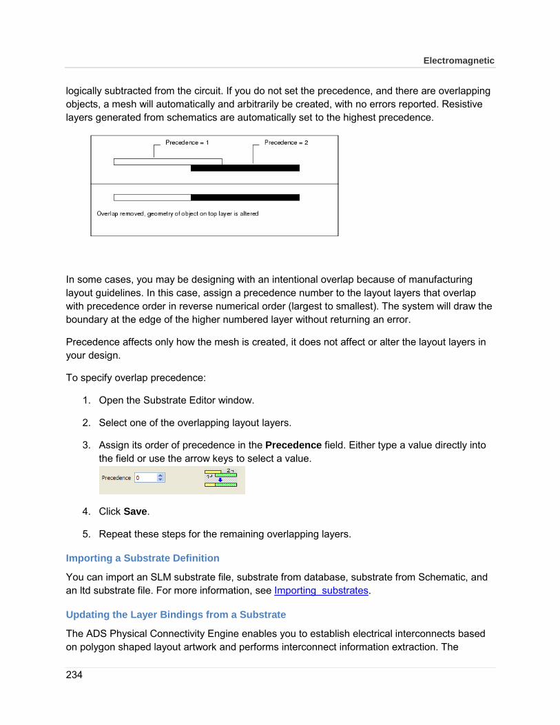
Electromagnetic
234
logically subtracted from the circuit. If you do not set the precedence, and there are overlapping objects, a mesh will automatically and arbitrarily be created, with no errors reported. Resistive layers generated from schematics are automatically set to the highest precedence.
In some cases, you may be designing with an intentional overlap because of manufacturing layout guidelines. In this case, assign a precedence number to the layout layers that overlap with precedence order in reverse numerical order (largest to smallest). The system will draw the boundary at the edge of the higher numbered layer without returning an error.
Precedence affects only how the mesh is created, it does not affect or alter the layout layers in your design.
To specify overlap precedence:
1. Open the Substrate Editor window.
2. Select one of the overlapping layout layers.
3. Assign its order of precedence in the Precedence field. Either type a value directly into the field or use the arrow keys to select a value.
4. Click Save.
5. Repeat these steps for the remaining overlapping layers.
Importing a Substrate Definition
You can import an SLM substrate file, substrate from database, substrate from Schematic, and an ltd substrate file. For more information, see Importing substrates.
Updating the Layer Bindings from a Substrate
The ADS Physical Connectivity Engine enables you to establish electrical interconnects based on polygon shaped layout artwork and performs interconnect information extraction. The

235
Physical Connectivity Engine requires a proper definition of the shape and pin layer binding. The layer binding setup can be derived automatically from a valid Momentum or FEM substrate setup. For more information on the Physical Connectivity Engine, refer to Physical Connectivity Engine
1. Click Edit Layer ( ) to open the Layer Definition window.
2. Click Update Layer Bindings to synchronize the layer bindings from the substrate setup. The Update Layer Binding dialog box is displayed.
3. Select the required substrate.
4. Click OK. An information dialog box is displayed to confirm that the layer bindings are updated.
The layer binding rules applied are:
1. All layout layers mapped at a specific dielectric interface (as STRIP or SLOT) or through a specific dielectric layer (as VIA) will bind.
2. Every via layer additionally binds to all strip layers just above, just below, or somewhere along the via.
3. The layer binding of layout layers that are not mapped will be cleared.
Caution SLOT layers require special attention! With this command, SLOT layers only bind to themselves or to other SLOT layers mapped at the same interface. The interconnect highlighting will not go through a SLOT layer. If you want a different behavior, you have to update the layer binding manually.
Saving a Substrate
A substrate definition can be saved to a file. This enables you to store the definition outside of the current project, making it easier to use the substrate definition in other designs. For more information, see Saving a Substrate.
A substrate definition file is saved with file extension .subst by default.
Viewing Substrate Computation Status After the substrate calculations are started, any messages regarding the calculations will appear in the Momentum Status window. Messages usually refer to any errors found, and indicate when the calculations are complete.
If you close the status window and want to reopen it, from the Layout menu bar choose Window > Simulation Status.
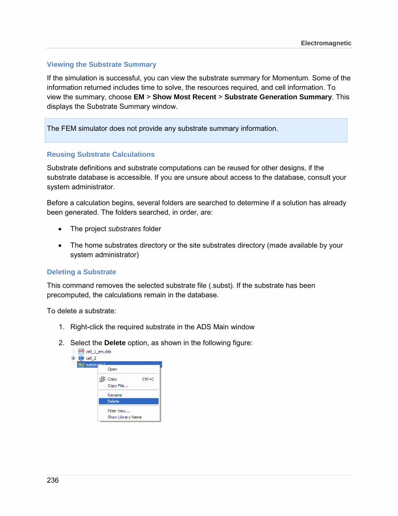
Electromagnetic
236
Viewing the Substrate Summary
If the simulation is successful, you can view the substrate summary for Momentum. Some of the information returned includes time to solve, the resources required, and cell information. To view the summary, choose EM > Show Most Recent > Substrate Generation Summary. This displays the Substrate Summary window.
The FEM simulator does not provide any substrate summary information.
Reusing Substrate Calculations
Substrate definitions and substrate computations can be reused for other designs, if the substrate database is accessible. If you are unsure about access to the database, consult your system administrator.
Before a calculation begins, several folders are searched to determine if a solution has already been generated. The folders searched, in order, are:
• The project substrates folder
• The home substrates directory or the site substrates directory (made available by your system administrator)
Deleting a Substrate
This command removes the selected substrate file (.subst). If the substrate has been precomputed, the calculations remain in the database.
To delete a substrate:
1. Right-click the required substrate in the ADS Main window
2. Select the Delete option, as shown in the following figure:
237
Substrate Definition Summary
For every change to a substrate definition, you need to recompute. The system checks for duplicate definitions, regardless of the name and uses previously computed data if it exists. The entire substrate definition includes:
• Vias, in the same manner that they are part of the fabrication process.
• Air bridges, including their height and their associated vias.
• Holes in ground planes, if they are part of a slot signal path (slot or coplanar), or if they are relief holes for vias passing through a ground plane are also part of the media.
• Dielectric layer properties (Er, MUr, and loss).
• Ground plane losses and cover properties (conductivity or impedance).
• Thick Conductors up or down.
Not included as part of the substrate definition:
• Metal loss of strip and via layers
The numerical computation process, used by the substrate calculator, can take as little as one minute for stripline circuits. It can take several minutes for microstrip or even a few hours for an arbitrary multi-layered substrate with several vias.
4.9 Using an EM Setup Template While creating an EM Setup view, the data fields of the view are initialized with hard-coded factory default settings. To override these settings, you can install an EM setup template with user-defined default settings in a library. You can use the settings for Simulator, Substrate, Frequency Plan, Output Plan, Momentum Options, FEM Options, Compute Resources, and EM Model found in the template to initialize a new EM Setup view.
To create a new EM Setup view, all open libraries (i.e. the library itself and all referenced libraries) are queried to get a list of available EM Setup templates. You can choose one of the following options:
• If the list is empty, the factory default settings are used.
• If the list holds one entry, the default settings are used silently.
• If the list holds more entries, a dialog box is displayed, which asks you to choose a setup.

Electromagnetic
238
4.9.1 Installing an EM Setup Template in a Library
To add an EM Setup template:
1. Create a (dummy) EM Setup cellview in the library, e.g. <libname>:<cellName>:<emSetupViewName>, and initialize its data.
2. From the ADS Main window, select Tools > Command Line to open the ADS Command Line Editor.
3. Type the following AEL command:
deemif_installSetupViewAsTemplateInLibrary("<libName>", "<cellName>", "<emSetupViewName>", "<emSetupTemplateName>")
The template gets installed in the library and a file with the name <emSetupTemplateName>.emsetup is saved in the library. After installation, you can delete the cell view.
4.9.2 Removing an EM Setup Template from a Library
To remove an EM Setup template from a library:
1. From the ADS Main window, select Tools > Command Line to open the ADS Command Line Editor.
2. Type the following AEL command:
dex_em_removeEmSetupTemplateFromLibrary("<libName>", "<emSetupTemplateName>")
4.10 Using the Job Manager
You can manage non-interactive processing jobs by using the Job Manager window. A new managed job is automatically created for various time-consuming operations. These operations currently include physical EM simulations and 3D model generations. The Job Manager window provides a user interface to show the job status and messages, and allows you to cancel running jobs. However, its scope is currently limited to physical EM simulation-related jobs.

239
The Job Manager consists of an internal queuing concept. According to this concept, jobs submitted with the same queue name run sequentially. Queues can be suspended and resumed. Note that this internal queuing system is complimentary to the queuing system of distributed job management systems such as Platform LSF and Sun Grid Engine. For circuit simulation job management, refer Circuit Remote Simulation.
Besides running locally, physical EM simulation setups can be configured to run on a remote host or a submission host for a distributed cluster. The Job Manager maintains a PVM cluster of hosts ready to accept jobs, and dynamically adds hosts to the cluster as needed. Complete cluster host configuration and management capabilities are provided inside the Job Manager user interface.
4.10.1 Starting the Job Manager
A Job Manager window is automatically displayed in the background when an EM Setup is
opened or a physical EM simulation is started. It can be brought to the front by clicking icon on the task bar.
Alternatively, you can display the Job Manager window by using the EM Setup window. Perform the following steps:
1. Select EM > Simulation Setup to open the EM Setup window.
2. Select Resources in the left pane of the EM Setup window.

Electromagnetic
240
3. Click the Start button in Job Manager, as shown in the following figure:
4. The Job Manager main window is displayed, which lists a summary of all jobs created since the Job Manager was launched:
Warning The Job Manager window closes automatically if the main window is closed. If

241
active jobs are still pending, a message box is displayed asking for confirmation. After confirmation, these jobs will be canceled without cleaning up their working directories. All status and logging information is discarded at exit. If you just want to hide the main window, minimize it instead of closing it. One exception: jobs that are actively running on a 3rd party cluster survive closing and reopening the Job Manager. To access these jobs, reopen the Job Manager from an EM Setup and the jobs will reappear in the main Job Manager window.
5. Double-click a job entry to view detailed log messages.
Note This log window is immediately displayed when newly created jobs do not need to wait in the internal queuing system. Select View > Show Main Window to open the main window from here. Newly created jobs that have to wait in a Job Manager queue will open the main window and highlight the summary line.
4.10.2 Job Progression
All jobs progress through the following states:
1. Creating a new job: A new job is created and the following job configuration information is displayed in the topmost part of the detailed log window.
o ADS Workspace::Design: Specifies the workspace and design being simulated.

Electromagnetic
242
o Simulator: Specifies the simulator Momentum or FEM used for simulation.
o Input/output directory: Specifies the directory used for containing input files and output files.
o Working directory: Specifies the host directory where the job will perform the main task. This can be the same directory as the input/output directory.
2. Queuing... or Queuing (queue suspended): After a job is created, it needs to wait until earlier jobs in the same Job Manager queue are complete.
3. Connecting with the remote host: The remote host is not yet part of the PVM cluster and is currently being dynamically added to the cluster.
4. Preparing Files: This preparation step consists of the following stages:
o The input/output directory and working directory are locked to prevent double usage. The lockfile is an empty directory named .simlock.
o Local preparation work is performed in the input/output directory.
o The contents of the input/output directory are copied to the working directory.
5. Performing the main task: The job is inside its main task. In the Local/remote mode, the status displays Running. For the Distributed mode, the following third-party cluster submission and status tracking is performed:
o Submitting to cluster
o Cluster response: submitted. In response to choosing Job > Query Status:
o Requesting status update
o Cluster response: created/submitted/pending/running/suspended/ended or Cluster did not answer
6. Waiting: This step allows dying processes and network disk operations to settle.
7. Retrieving results: The contents of the working directory are copied back to the input/output directory.
8. Processing results: The final datasets are installed in this step.
9. Cleaning up: The working directory is cleaned up (only if this is not also the input/output directory). The .simlock lockfile is removed from the input/output directory.
10. Done
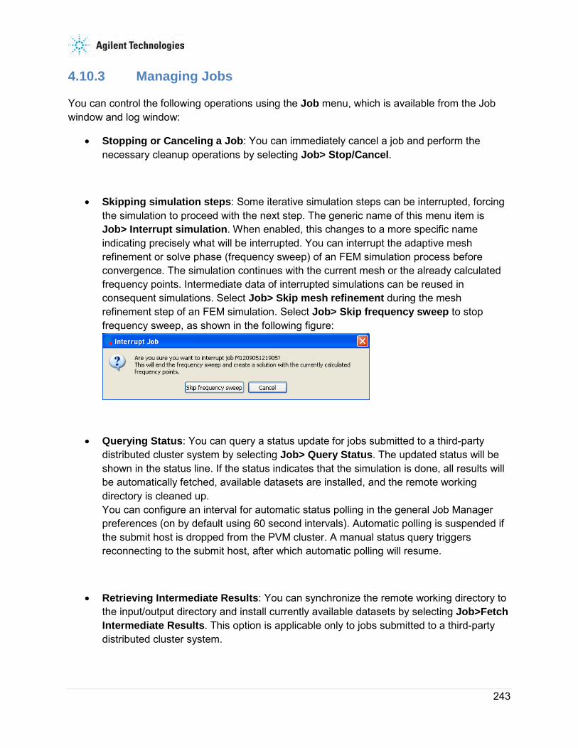
243
4.10.3 Managing Jobs
You can control the following operations using the Job menu, which is available from the Job window and log window:
• Stopping or Canceling a Job: You can immediately cancel a job and perform the necessary cleanup operations by selecting Job> Stop/Cancel.
• Skipping simulation steps: Some iterative simulation steps can be interrupted, forcing the simulation to proceed with the next step. The generic name of this menu item is Job> Interrupt simulation. When enabled, this changes to a more specific name indicating precisely what will be interrupted. You can interrupt the adaptive mesh refinement or solve phase (frequency sweep) of an FEM simulation process before convergence. The simulation continues with the current mesh or the already calculated frequency points. Intermediate data of interrupted simulations can be reused in consequent simulations. Select Job> Skip mesh refinement during the mesh refinement step of an FEM simulation. Select Job> Skip frequency sweep to stop frequency sweep, as shown in the following figure:
• Querying Status: You can query a status update for jobs submitted to a third-party distributed cluster system by selecting Job> Query Status. The updated status will be shown in the status line. If the status indicates that the simulation is done, all results will be automatically fetched, available datasets are installed, and the remote working directory is cleaned up. You can configure an interval for automatic status polling in the general Job Manager preferences (on by default using 60 second intervals). Automatic polling is suspended if the submit host is dropped from the PVM cluster. A manual status query triggers reconnecting to the submit host, after which automatic polling will resume.
• Retrieving Intermediate Results: You can synchronize the remote working directory to the input/output directory and install currently available datasets by selecting Job>Fetch Intermediate Results. This option is applicable only to jobs submitted to a third-party distributed cluster system.

Electromagnetic
244
Note It is not necessary to use Job > Fetch Intermediate Results at the end of a distributed simulation. Use Job > Query Status instead, which additionally cleans up the remote working directory and notifies other tools of the completion of the simulation.
• Deleting logs: You can completely remove a job from the Job Manager by selecting Job > Delete Log in the main window.
Warning When using Job > Delete Log on a running job, a message box is displayed asking for confirmation. After confirmation, this job will be canceled without cleaning up its working directory. To avoid this, use Job > Stop/Cancel Job and delete the job only after the status has changed to Done.
The Job Manager provides a simple queuing system where jobs submitted with the same queue name run sequentially. The queue name is specified in the EM Setup. For more information, see Specifying Simulation Resources. For complex queue management, use a dedicated job management tool such as Platform LSF and Sun Grid Engine. Job manager queues can be suspended and resumed by selecting a queued job in the main menu and choosing Queue > Suspend Queue or Queue > Resume Queue.
Note It is not possible to suspend a queued job once the job has started. Still, Queue > Suspend Queue can be used to suspend execution of subsequent queued jobs. After a queue completes, it will automatically enter a suspended state. Use Resources > Simulation Resources > Auto-start queue after submission in the EM Setup if you want to automatically (re)start the queue when submitting a new simulation.
4.10.4 Managing Hosts
Select View > Hosts from the main Job Manager window to display the status of all hosts in the PVM cluster. This window will also automatically pop up whenever hosts are dynamically being added to the cluster.
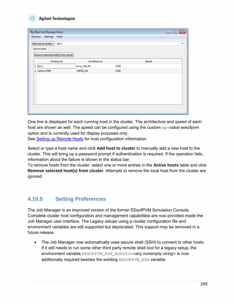
245
One line is displayed for each running host in the cluster. The architecture and speed of each host are shown as well. The speed can be configured using the custom sp=value eesofpvm option and is currently used for display purposes only. See Setting up Remote Hosts for host configuration information.
Select or type a host name and click Add host to cluster to manually add a new host to the cluster. This will bring up a password prompt if authentication is required. If the operation fails, information about the failure is shown in the status bar. To remove hosts from the cluster, select one or more entries in the Active hosts table and click Remove selected host(s) from cluster. Attempts to remove the local host from the cluster are ignored.
4.10.5 Setting Preferences
The Job Manager is an improved version of the former EEsofPVM Simulation Console. Complete cluster host configuration and management capabilities are now provided inside the Job Manager user interface. The Legacy setups using a cluster configuration file and environment variables are still supported but deprecated. This support may be removed in a future release.
• The Job Manager now automatically uses secure shell (SSH) to connect to other hosts. If it still needs to run some other third party remote shell tool for a legacy setup, the environment variable EESOFPVM_RSH_NOAUTO=<any nonempty string> is now additionally required besides the existing EESOFPVM_RSH variable.

Electromagnetic
246
• When migrating to the new GUI-based configuration, it is advised to remove all old eesofpvm configuration settings:
o If coexistence with ADS 2009 (Update 1) is not necessary, remove the cluster configuration file at <home directory>/hpeesof/config/pvmhost_cfg.txt and/or the path specified by the <home directory>/hpeesof/config/hpeesof.cfg variable EESOFPVMHOSTFILE (and remove this variable). However, if ADS 2009 (Update 1) coexistence is required, the legacy eesofpvm host file can still be obscured to the Job Manager by overriding the hpeesof.cfg variable EESOFPVMHOSTFILE with an additional variable EESOFPVMHOSTFILE:390=/nonexistent. The number 390 is the internal Job Manager version number as shown when choosing Help > About EEsof Job Manager from the main window.
o If coexistence with ADS 2009 (Update 1) is not necessary, eliminate all environment variables containing EESOFPVM in the name from the Windows environment or Unix init scripts (e.g. ~/.bashrc or ~/.kshrc) and the ~/.eesofpvmprofile file. The only environment variable that does not lose its relevance is EESOFPVM_TMP, the directory where the PVM daemon displays its configuration and writes logging information.
Choose Settings > Preferences from the Main window or the hosts window to open the Preferences dialog box. These preferences are saved in <home directory>/hpeesof/config/simsys.cfg, which can be distributed towards other users if they all use the same remote simulation hosts.

247
General Options
• Allow jobs to pop up their log: When selected, a new window pops up for each new job. Otherwise, new jobs will only be highlighted in the Job Summary list. It is selected by default.
• Automatically query 3rd party cluster status every xxx seconds: When selected, the status of jobs running on a 3rd party cluster will be automatically polled using fixed time intervals. Automatic polling is suspended if the submit host is dropped from the PVM cluster. A manual status query triggers reconnecting to the submit host, after which automatic polling will resume. This option is selected by default using an interval of 60 seconds.

Electromagnetic
248
Specifying Startup/Shutdown Configuration
The Job Manager runs as a task of the PVM cluster it controls. The PVM infrastructure needs to start before the Job Manager starts, and can be allowed to continue running after the Job Manager has exited. To accommodate different requirements, several startup/shutdown options are available. Refer to the following recommended settings:
• Start the eesofpvm backend when ADS starts: When selected, the PVM infrastructure will silently start when ADS is started. This reduces the response time to start the first simulation (at much lower cost). It is selected by default.
• Close EEsof Job Manager when ADS exits: When selected, the Job Manager will exit when ADS exits. A confirmation message box will appear when there are unfinished jobs. It is selected by default.
• Shut down the eesofpvm backend when both ADS and EEsof Job Manager have exited: When selected, the PVM infrastructure will be stopped when both ADS and EEsof Job Manager have exited. It is selected by default.
• Shut down the eesofpvm backend when EEsof Job Manager exits: When selected, the PVM infrastructure will be stopped when the EEsof Job Manager exits. This check box can be partially selected, which displays a message box asking for your confirmation. It is not selected by default.
• Use separate eesofpvm backends for different combination of user/host/$DISPLAY/$HPEESOF_DIR: When selected , all internal files that are shared between different executables of the same PVM session will get a suffix to separate different PVM sessions from one another. This prohibits conflicts between different PVM sessions running on the same system. The suffix consists of eight lowercase letters and/or digits. It is selected by default.
If the presence of a legacy PVM cluster configuration is detected (if EESOFPVMHOSTFILE is defined or $HOME/hpeesof/config/pvmhost_cfg.txt exists), the default settings will be different in order to mimic the original behavior:
Preference name Normal default (recommended)
Legacy default
Start the eesofpvm backend Selected Not selected
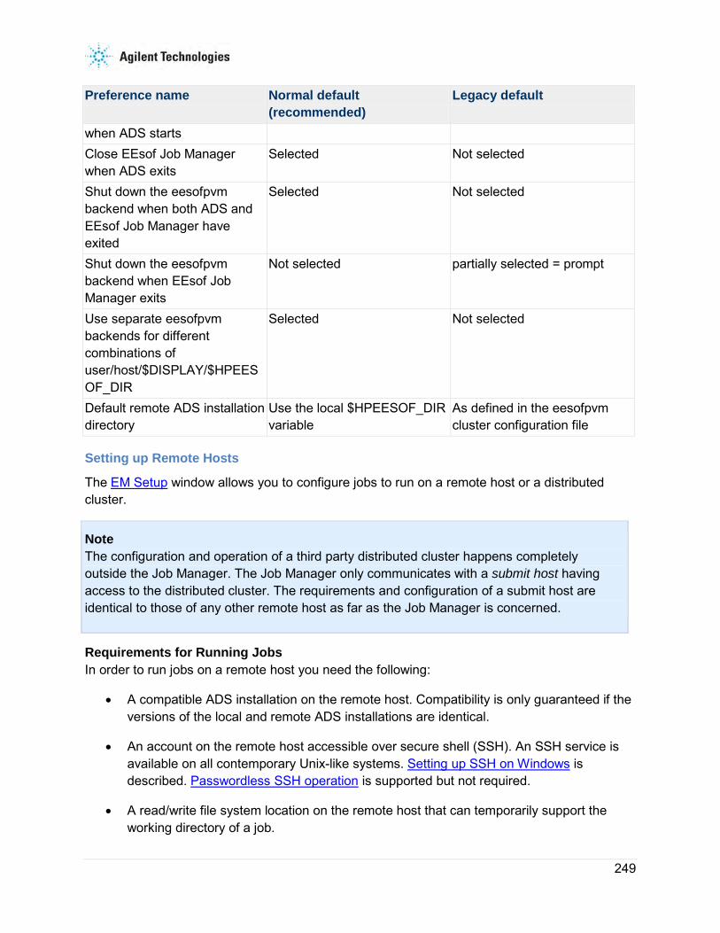
249
Preference name Normal default (recommended)
Legacy default
when ADS starts Close EEsof Job Manager when ADS exits
Selected Not selected
Shut down the eesofpvm backend when both ADS and EEsof Job Manager have exited
Selected Not selected
Shut down the eesofpvm backend when EEsof Job Manager exits
Not selected partially selected = prompt
Use separate eesofpvm backends for different combinations of user/host/$DISPLAY/$HPEESOF_DIR
Selected Not selected
Default remote ADS installation directory
Use the local $HPEESOF_DIR variable
As defined in the eesofpvm cluster configuration file
Setting up Remote Hosts
The EM Setup window allows you to configure jobs to run on a remote host or a distributed cluster.
Note The configuration and operation of a third party distributed cluster happens completely outside the Job Manager. The Job Manager only communicates with a submit host having access to the distributed cluster. The requirements and configuration of a submit host are identical to those of any other remote host as far as the Job Manager is concerned.
Requirements for Running Jobs In order to run jobs on a remote host you need the following:
• A compatible ADS installation on the remote host. Compatibility is only guaranteed if the versions of the local and remote ADS installations are identical.
• An account on the remote host accessible over secure shell (SSH). An SSH service is available on all contemporary Unix-like systems. Setting up SSH on Windows is described. Passwordless SSH operation is supported but not required.
• A read/write file system location on the remote host that can temporarily support the working directory of a job.

Electromagnetic
250
Configuring a Remote Host To configure a remote host, add a configuration line to the Host specific overrides:
Specify the following fields:
• Hostname: This is the DNS name of the remote host or its dotted IP address. If you want to limit the configuration to a specific ADS version, add :version and optionally additionally .revision after the host name. The current values for version and revision are shown on the first line of the dialog shown when choosing Help > About EEsof Job Manager from the main window: EEsof Job Manager (version.revision).
• ADS installation directory: This is the path to the main ADS installation directory.
• Working directory: The remote working directory is specified in the EM Setup window. The working directory entered in the Job Manager preferences is used as base directory to complete relative path specifications. However, if you append :force to the end of the path, the directory specified in the EM Setup is always ignored and the path preference is used exactly as specified. Environment variables specified as $VAR, ${VAR} or %VAR% are expanded on the remote host. Use ${VAR:local} or %VAR:local% to expand environment variables on the local host. Escape a literal $ as $$ and a literal % as %%. The following local variables have a special meaning:
o ${HOSTNAME:local}: the local hostname
o ${PWD:local}: the input/output directory
o ${SESSION:local}: an identifier unique to each PVM cluster instance (a string of eight lowercase letters and digits if Use separate eesofpvm backends for different combinations of user/host/$DISPLAY/$HPEESOF_DIR is selected, otherwise default)

251
o ${TAG:local}: a M012345678901 identifier for the job that is unique within the Job Manager session In case you want to avoid all directory conflicts, a good choice would be
%USERPROFILE%\Jobs\%SESSION:local%\%TAG:local%:force
for remote Windows hosts and
/var/tmp/$USER/jobs/${SESSION:local}/${TAG:local}:force
for remote Linux hosts.
• Additional eesofpvm options: Enter a list of space separated name=value options for PVM.
o lo=username specifies an alternate login name to use.
o dx=<path to eesofpvmd> specifies an alternate path to the eesofpvmd executable or script. For further options, consult the PVM documentation .
• Memory limit: This field specifies a hard limit for the memory available to individual job processes. It can be used to automatically stop jobs with an out of memory error before they use so much memory that the computer enters an unresponsive trashing state from which it is hard to recover. It does not allow you to run a simulation with less memory. This configuration option is applicable to local and remote processes, but not to processes running on 3rd party clusters. You can either specify unlimited, or an absolute amount of memory (xxxMB), or a negative offset from the total amount of RAM (RAM-xxxMB).
If the entries for ADS installation directory, Working directory or Memory limit are empty, the specified defaults are used. These defaults can be used to avoid redundant configuration repetitions. Each name specified in Default additional eesofpvm options is only overridden if the same name is specified in the Host specific overrides.
Mode of Operation The Job Manager window dynamically adds remote hosts to the PVM cluster as required or requested. A host is added as follows:
1. A secure shell (SSH) connection is initiated to the remote host.
Electromagnetic
252
2. The local host prompts for passwords.
3. The SSH connection is now established.
4. (Only on Unix remote hosts) The Bourne shell script file ~/.eesofpvmprofile is sourced if it exists. This file can be used to set additional environment variables. A typical use case is extending the PATH and LD_LIBRARY_PATH environment variables to ensure accessibility of the tools required to control a third party job management framework.
5. The PVM daemon is started on the remote host. The choice between 32-bit and 64-bit executables is automatic (64-bit executables are used whenever possible). The command used to start the PVM daemon is <ADS installation directory>/pvm3/bin/auto_eesofpvmd.exe.
6. The remote PVM daemon contacts the local PVM daemon over a dedicated TCP/IP connection. The remote host is now part of the PVM cluster and remains in the cluster until this connection is closed.
7. The SSH connection is closed. The remote PVM daemon keeps running.
Note In case of remote simulation issues, check your firewall configuration at both ends (try disabling it temporarily to check if there is an issue). Several executables in the ADS installation directory open outbound and/or inbound TCP/IP connections. The ports are always in the operating system's dynamic TCP/IP port range, except for SSH which uses port 22. On Windows versions prior to Windows Vista, the dynamic port range is 1025-65535. Windows Vista and later versions use the range 49152-65535. On Linux the dynamic port range is 32768-61000. Adjust the firewall rules to allow connections from/to these ports.
Setting up an SSH server on Windows The software package Copssh can be used to deploy a SSH server on a Windows host. A free version of this package is provided in the <ADS installation directory>\pvm3\tools\Copssh directory. Install the package using the suggested settings (administrator privileges are required). Do not attempt to change the autogenerated password for the SvcCOPSSH user (remembering this password is also not necessary).
Follow these steps for each user:
1. Log on as a user having administrative privileges (possibly but not necessarily the user to be activated).
2. Launch Start > Copssh > 01. Activate a user.

253
o Enter the name of an existing user on the host. The short %USERNAME% login name is required, not a first and last name. This name will be the login name for SSH. If the user name exists inside a Windows domain, prefix the user name with the domain name and a backslash (these items are not part of the login name for SSH).
o Use /bin/bash as command shell
o Select Remove copssh home directory if it exists.
o Do not select Create keys for public key authentication.
o Select Create link to user's real home directory.
3. Click Next. An acknowledgment message is displayed.
4. Click OK.
5. Browse to the required directory C:\Program Files\ICW\home/username (C:\Program Files (x86)\ICW\home/username on a 64-bit system).
6. Open the file .bashrc with a text editor. It is important to use an editor that upholds end-of-line conventions (do not use Notepad). A suitable editor is Notepad++ , which is provided as <ADS installation directory>\pvm3\tools\Notepad+\notepad+.exe.
7. At the end of the .bashrc file, add an empty line followed by the following lines:
export EESOFPVM_TMP="$USERPROFILE\\PVM" export HOME="$USERPROFILE" cd
Note Make sure that the file ends again with an empty line.
8. Save the .bashrc file and exit the editor.
9. Log on as the user to be activated and open a command prompt (Start > Run > cmd.exe)
10. Execute mkdir "%USERPROFILE%\PVM" in the command prompt.
11. Close the command prompt.
12. The user account is now accessible through ssh.

Electromagnetic
254
You can verify correct operation by using the shell login command ssh <user>@<hostname> from a Unix terminal or from a Windows command prompt (choose Start > Run > cmd.exe, then first type cd <ADS installation directory>\tools\bin <return>). Log on over SSH and run <ADS installation directory>/pvm3/bin/auto_eesofpvmd.exe (replace all backslashes by forward slashes). If the output ends with a short string resembling either 7f000001:d789 or /tmp/eesofpvmtmp025108.0, configuration was successful (the exact (hexa)decimal digits can be different). Otherwise an error message indicating the problem is shown (messages about an unreadable file pvmhost_cfg.txt are normal and can be safely ignored).
Note When accessing a Windows host remotely, network shares are generally not available as drive letters. When referring to remote network drives, use the UNC name (<double backslash> <hostname> <backslash> <sharename>) instead of the drive letter.
The Copssh installer assigns some special rights to the administrative SvcCOPSSH user in order to support passwordless operation. However, when the host is part of a Windows domain, the domain's security policy is often configured to periodically reject these rights to all users, rendering Copssh unusable. Typically Copssh appears to be working after installation, but all SSH logins fail the next day (as a result of the domain's security policy being applied overnight).
To permanently fix this issue:
1. Make sure you are logged in as a user in the Administrators group.
2. Move the file C:\Program Files\ICW\etc\sshd_config (C:\Program Files (x86)\ICW\etc\sshd_config on a 64-bit system) to a writeable location, such as the Desktop.
3. Open the moved file with a text editor. It is important to use an editor that upholds end-of-line conventions (do not use Notepad). A suitable editor is Notepad++ , which is provided as <ADS installation directory>\pvm3\tools\Notepad+\notepad+.exe.
4. Find the following line of text:
#PubkeyAuthentication yes
5. Change this line into (be sure to remove the pound sign):
PubkeyAuthentication no
6. Save sshd_config and exit the text editor.

255
7. Move sshd_config back to its original position.
8. Open the Services control panel (As privileged user, choose Start > Run > services.msc).
9. Double-click the entry for Openssh SSHD.
10. Stop the service.
11. In the Log On tab, change Log on as: to use Local System Account instead of the SvcCOPSSH user.
12. Click Apply.
13. Go back to the General tab and start the service.
After this fix, you cannot connect to the remote machine without specifying the password, yet normal password-based operation work again. If you plan to use password-based operation, this fix can be applied up-front (without running into the issue first).
Passwordless SSH Operation SSH can be configured to use public key authentication without the need to enter a password. In this mode of authentication, the local host presents a private key that must match a public key known to the remote host. Perform the following steps:
1. Generate the public/private key pair on the local host (the one that runs the Job Manager)
a. On Windows, open a command prompt (Start > Run > cmd.exe) and type cd <ADS installation directory>\tools\bin <return>. On Unix, open a terminal.
b. Type ssh-keygen -t dsa <return>. Just hit the return key when prompted for the file location and the passphrase.
c. Remember the location of the public key which is displayed.
2. Copy the public key id_dsa.pub from the local host to the remote host.
3. On the remote host, check for the existence of the .ssh directory and create it if missing. This directory must have read/write rights for the targeted user, and no rights assigned to anyone else. On Windows, the .ssh directory is C:\Program Files\ICW\home/username/.ssh (C:\Program Files (x86)\ICW\home/username/.ssh on a 64-bit system). On Unix, the .ssh directory is ~/.ssh.
4. On the remote host, append the contents of id_dsa.pub to <.ssh directory>/authorized_keys. This file must not be writeable by other users than the

Electromagnetic
256
targeted user. If the authorized_keys file did not yet exist, just rename id_dsa.pub to authorized_keys instead of creating an empty file and appending.
The configuration is now complete. If passwordless operation does not appear to work in the Job Manager, verify operation using the shell login command ssh <user>@<hostname> from a Unix terminal or from a Windows command prompt (choose Start > Run > cmd.exe, then first type cd <ADS installation directory>\tools\bin <return>).
Warning On Windows remote machines, network shares on the remote machine may refuse operation in passwordless mode because the user is not authenticated to the Windows domain.
Specifying Configuration Files and Environment Variables
Specifying Job Manager Preferences The Job Manager preferences are stored as <name>=<value> lines in the file <home directory>/hpeesof/config/simsys.cfg. These settings override those in the file <ADS installation directory>/custom/config/simsys.cfg, which in its turn overrides settings in the file <ADS installation directory>/config/simsys.cfg. The file <ADS installation directory>/custom/config/simsys.cfg can be used for site-wide deployment of Job Manager preferences. Note however that the Job Manager GUI will always incrementally save preference changes to the file <home directory>/hpeesof/config/simsys.cfg.
The preferences are mapped to the simsys.cfg file as follows:
Preference name Variable name in simsys.cfg
Acceptable values
Allow jobs to pop up their log JOB_LOG_POPUP TRUE or FALSE Automatically query 3rd party cluster status
AUTOQUERY_CLUSTER TRUE or FALSE
Interval between queries in seconds
AUTOQUERY_CLUSTER_INTERVAL
integer
Start the eesofpvm backend when ADS starts
ADS_STARTS_EESOFPVM TRUE or FALSE
Close EEsof Job Manager when ADS exits
ADS_STOPS_JOBMANAGER TRUE or FALSE
Shut down the eesofpvm STOP_ORPHAN_EESOFPVM TRUE or FALSE
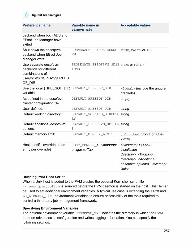
257
Preference name Variable name in simsys.cfg
Acceptable values
backend when both ADS and EEsof Job Manager have exited Shut down the eesofpvm backend when EEsof Job Manager exits
JOBMANAGER_STOPS_EESOFPVM
TRUE, FALSE or ASK
Use separate eesofpvm backends for different combinations of user/host/$DISPLAY/$HPEESOF_DIR
SEGREGATE_EESOFPVM_SESSIONS
TRUE or FALSE
Use the local $HPEESOF_DIR variable
DEFAULT_HPEESOF_DIR <local> (include the angular brackets)
As defined in the eesofpvm cluster configuration file
DEFAULT_HPEESOF_DIR empty
User defined: DEFAULT_HPEESOF_DIR string Default working directory: DEFAULT_WORKING_DIRECTO
RY string
Default additional eesofpvm options:
DEFAULT_EESOFPVM_OPTIONS
string
Default memory limit: DEFAULT_MEMORY_LIMIT unlimited, xxxMB or RAM-xxxMB
Host specific overrides (one entry per override)
HOST_CONFIG_<unimportant unique suffix>
<Hostname>|<ADS installation directory>|<Working directory>|<Additional eesofpvm options>|<Memory limit>
Running PVM Boot Script When a Unix host is added to the PVM cluster, the optional Korn shell script file ~/.eesofpvmprofile is sourced before the PVM daemon is started on the host. This file can be used to set additional environment variables. A typical use case is extending the PATH and LD_LIBRARY_PATH environment variables to ensure accessibility of the tools required to control a third party job management framework.
Specifying Environment Variables The optional environment variable EESOFPVM_TMP indicates the directory in which the PVM daemon advertises its configuration and writes logging information. You can specify the following settings:

Electromagnetic
258
• Windows: the environment variable TEMP, or if this is unset, C:\TEMP
• Unix: /tmp
Specifying Legacy Settings The following settings are deprecated but supported for legacy setups:
• The PVM cluster configuration file: this is by default <home directory>/hpeesof/config/pvmhost_cfg.txt. Its path can be overridden by the <home directory>/hpeesof/config/hpeesof.cfg variable EESOFPVMHOSTFILE.
• The environment variable EESOFPVM_RSH pointing to a remote shell executable. This variable now additionally requires EESOFPVM_RSH_NOAUTO=<any nonempty string> to be set in order to be recognized.

259
Chapter 5 – Ports • Defining Ports in EM Simulations
• Setting up Ports
• Using Ports in Momentum
o Momentum Ports Overview
o Using Calibrated Ports
o Using Uncalibrated Ports
• Using Ports in FEM
5.1 Defining Ports in EM Simulations
To determine how an EM model can interconnect with other components in a schematic, you need to configure ports for the EM model generation. Using the EM Setup window, you can improve the use model of the port setup process. You can refresh layout pins information, create, delete, sequence ports, and search the required S-parameter ports or layout pins. It provides the following benefits:
• Provides easier editing or viewing capability.
• Provides flexible S-parameter port setup capability.
• Assists in setting up S-parameter ports.
Note The port definitions are stored with the layout. Therefore, it is recommended to enable the Save all designs when simulation starts preference from the main window of PDE.
5.1.1 Assigning a Layout Pin to the S-parameter Port
Momentum and FEM generate N-port S-parameter models for your circuit. The S-parameter Ports define the input/output locations where current can be injected and/or measured and/or exchanged. They are also required to connect the physical structure with other electrical circuit components in an EM circuit cosimulation.

Electromagnetic
260
Each port consists of two terminals, terminal (signal) and terminal (reference). The port current flows from the + terminal into the circuit and leaves the circuit via the - terminal. The port voltage is defined as the difference of the electric scalar potential between the two terminals:
Vp = V(r+) - V(r-)
Note The scalar potential V(r) at infinity is zero.
S-parameters model the difference in voltage between the + and - terminal only. One never knows the absolute voltage of the reference terminal(s). On a schematic, an N-port S-parameter model can have either N+1 or 2N terminals. The two are equivalent because you don't know the absolute voltage at any of the N reference terminals. It doesn't matter if you short them all together or not. In case of 2N terminals, only the voltage difference will be applied to the S-parameter model.
While the + terminal is always explicitly defined, the - terminal can be defined in the following ways:
• When there is an infinite ground plane, the - terminal is implicitly located in the infinite ground plane closest to the + terminal.
• In the absence of an infinite ground plane, the - terminal needs to be explicitly defined somewhere close to the + terminal.
• For Momentum, when there is no - terminal and no infinite ground plane, the port voltage is defined as the value of the electric scalar potential at the + terminal: Vp = V(r+). You can rewrite this as follows:
Vp = V(r+) -- V (at infinity)
Therefore, you can consider infinity as the location of the implicit - terminal for this case. For FEM, - terminals need to be define in all cases in absence of an infinite ground.
Ports are defined in a two-step process. First, layout pins are added to the circuit layout. These pins define the places where current can enter or leave the circuit. Then, using the EM Setup window,, you specify how the layout pins are used to define S-parameter ports in an EM simulation.
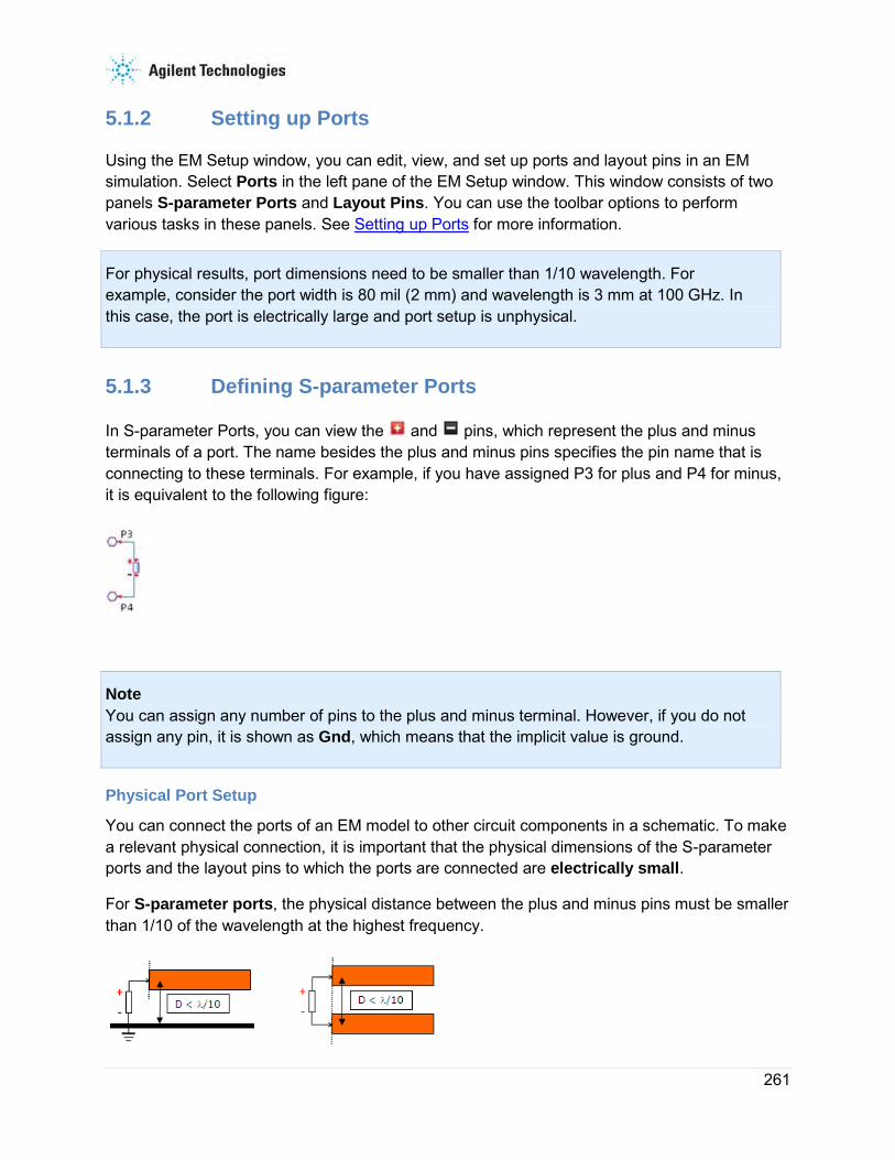
261
5.1.2 Setting up Ports
Using the EM Setup window, you can edit, view, and set up ports and layout pins in an EM simulation. Select Ports in the left pane of the EM Setup window. This window consists of two panels S-parameter Ports and Layout Pins. You can use the toolbar options to perform various tasks in these panels. See Setting up Ports for more information.
For physical results, port dimensions need to be smaller than 1/10 wavelength. For example, consider the port width is 80 mil (2 mm) and wavelength is 3 mm at 100 GHz. In this case, the port is electrically large and port setup is unphysical.
5.1.3 Defining S-parameter Ports
In S-parameter Ports, you can view the and pins, which represent the plus and minus terminals of a port. The name besides the plus and minus pins specifies the pin name that is connecting to these terminals. For example, if you have assigned P3 for plus and P4 for minus, it is equivalent to the following figure:
Note You can assign any number of pins to the plus and minus terminal. However, if you do not assign any pin, it is shown as Gnd, which means that the implicit value is ground.
Physical Port Setup
You can connect the ports of an EM model to other circuit components in a schematic. To make a relevant physical connection, it is important that the physical dimensions of the S-parameter ports and the layout pins to which the ports are connected are electrically small.
For S-parameter ports, the physical distance between the plus and minus pins must be smaller than 1/10 of the wavelength at the highest frequency.

Electromagnetic
262
For layout pins, the length of the edge (layout pins at an edge of the structure) or the diameter of the area (layout pins inside the structure) must be smaller than 1/10 of the wavelength at the highest frequency.
The physical port setup restrictions stem from circuit theory that stipulates that all physical dimensions are electrically small so that no phase delays are present in the circuit. Failing to comply with the physical port setup restrictions, generates unphysical circuit S-parameters.
Note To comply with the physical port setup, S-parameter ports for circuits with no infinite ground plane in the substrate should always be defined between two explicit layout pins.
In the S-parameter Ports panel, you can perform the following tasks:
• Viewing S-parameter Ports
• Editing the S-parameter Ports Properties
• Selecting the S-Parameter Ports Title Fields
5.1.4 Selecting the Reference Offset
The calibrated ports enable you to shift the location of the reference lines used for the S-parameters. You can select the following types of reference offsets:
• Specifying a positive reference offset: Shifts the reference planes in the direction towards the circuit, as shown in the following figure:

263
• Specifying a negative reference offset: Shifts the reference planes in the direction away from the circuit, as shown in the following figure:
Why Use Reference Offsets?
The need to adjust the position of ports in a layout is analogous to the need to eliminate the effect of probes when measuring hardware prototypes. When hardware prototypes are measured, probes are connected to the input and output leads of the Device Under Test (DUT). These probes feed energy to the DUT, and measure the response of the circuit. However, the measured response characterizes the entire setup, that is, the DUT plus the probes. This is an unwanted effect. The final measurements should reflect the characteristics of the DUT alone. The characteristics of the probes are well known, so measurement labs can mathematically eliminate the effects of the probes, and present the correct measurements of the DUT.
There are significant resemblances between this hardware measurement process and the way Momentum and FEM operate. In the case of Momentum and FEM, the probes are replaced by ports, which, during simulation, will feed energy to the circuit and measure its response. The port feeding scheme also has its own, unwanted effect: low-order mode mismatch at the port boundary, although this is eliminated by the calibration process.
However, for a calibration process, it is necessary that the fundamental mode is characterized accurately. This can only be accomplished when the distance between the port boundary and the first discontinuity is sufficiently large, that is, there exists a feed line that is long enough to provide this distance.
As a basic example, consider a line width that varies abruptly in some part of your circuit, as shown in the following figure:

Electromagnetic
264
You need to characterize only the variation of the step-in-width itself, as shown in the following figure:
As mentioned previously, it takes a little distance for the fundamental mode to settle, which means that this short structure might not yield the accuracy that you expect from the simulation. In this case, allow for some feed line length, as shown in the following figure:
Now, the simulation will yield accurate results, but the results will also contain the extra line lengths. To resolved this issue, use reference offsets. Although, the circuit has been calculated with the long lines, reference offset shifting allows you to produce the S-parameters as if the short structure had been simulated instead, as shown in the following figure:
The effect of the extra feed lines is mathematically eliminated from the S-parameter solution. This process of adding or subtracting line length is generally referred to as de-embedding. During the solution process, the impedance and propagation constant has been calculated for the ports, based on their physical location in the circuit. When you know the impedance, propagation constant, and the distance of de-embedding, you can cancel out the extra lengths of line from the S-parameter results, by compensating for the loss and phase shifts of those lines. The net result is a set of S-parameters, calculated as if the extra line lengths were not there.
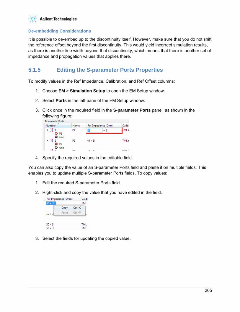
265
De-embedding Considerations
It is possible to de-embed up to the discontinuity itself. However, make sure that you do not shift the reference offset beyond the first discontinuity. This would yield incorrect simulation results, as there is another line width beyond that discontinuity, which means that there is another set of impedance and propagation values that applies there.
5.1.5 Editing the S-parameter Ports Properties
To modify values in the Ref Impedance, Calibration, and Ref Offset columns:
1. Choose EM > Simulation Setup to open the EM Setup window.
2. Select Ports in the left pane of the EM Setup window.
3. Click once in the required field in the S-parameter Ports panel, as shown in the following figure:
4. Specify the required values in the editable field.
You can also copy the value of an S-parameter Ports field and paste it on multiple fields. This enables you to update multiple S-parameter Ports fields. To copy values:
1. Edit the required S-parameter Ports field.
2. Right-click and copy the value that you have edited in the field.
3. Select the fields for updating the copied value.

Electromagnetic
266
4. Right-click and paste the value on the selected fields, as shown in the following figure:
S-parameter Port Grouping
The calibration process automatically groups S-parameter ports with terminals attached to layout pins that share a common reference plane. The following figure displays a grouped port:
5.1.6 Selecting the Calibration Type
You should select the calibration type based on the type of circuit component you want to connect to the port in the schematic. You can select TML and TML (zero length) calibration only for the S-parameter ports that have associated layout pins located at an edge of the structure. You can select SMD and Delta gap only for S-parameters ports that have two associated layout pins located at the edges of a gap in the structure. For S-parameter ports which have at least one associated layout pin inside the structure, None is the only option that can be selected as calibration type. Depending on your circuit component, you can select the following types of calibration:
• TML: Connects a transmission line component.
• TML(zero length): Connects a lumped component.
• SMD: Connects a 2-pin SMD component (model includes parasitics).
• Delta gap: Connects a 2-pin SMD component (model does not include parasitics).
• None: If none of the available calibration types is valid for the connecting component, specify None.
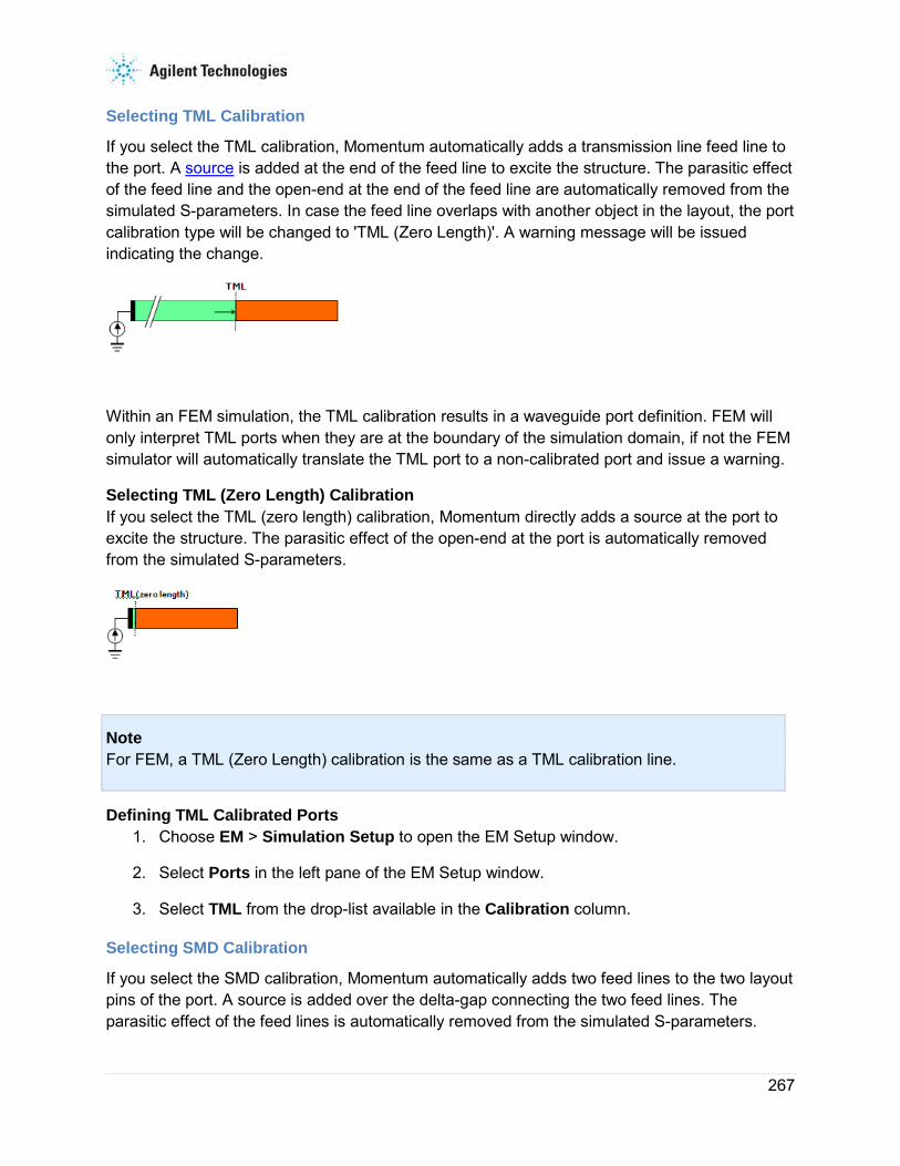
267
Selecting TML Calibration
If you select the TML calibration, Momentum automatically adds a transmission line feed line to the port. A source is added at the end of the feed line to excite the structure. The parasitic effect of the feed line and the open-end at the end of the feed line are automatically removed from the simulated S-parameters. In case the feed line overlaps with another object in the layout, the port calibration type will be changed to 'TML (Zero Length)'. A warning message will be issued indicating the change.
Within an FEM simulation, the TML calibration results in a waveguide port definition. FEM will only interpret TML ports when they are at the boundary of the simulation domain, if not the FEM simulator will automatically translate the TML port to a non-calibrated port and issue a warning.
Selecting TML (Zero Length) Calibration If you select the TML (zero length) calibration, Momentum directly adds a source at the port to excite the structure. The parasitic effect of the open-end at the port is automatically removed from the simulated S-parameters.
Note For FEM, a TML (Zero Length) calibration is the same as a TML calibration line.
Defining TML Calibrated Ports 1. Choose EM > Simulation Setup to open the EM Setup window.
2. Select Ports in the left pane of the EM Setup window.
3. Select TML from the drop-list available in the Calibration column.
Selecting SMD Calibration
If you select the SMD calibration, Momentum automatically adds two feed lines to the two layout pins of the port. A source is added over the delta-gap connecting the two feed lines. The parasitic effect of the feed lines is automatically removed from the simulated S-parameters.
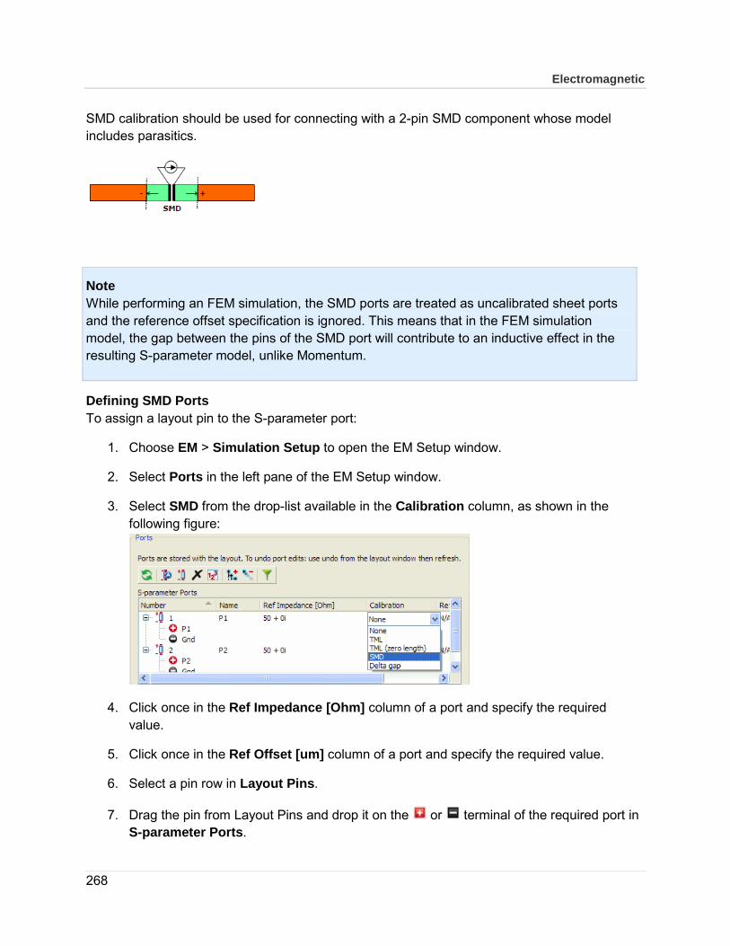
Electromagnetic
268
SMD calibration should be used for connecting with a 2-pin SMD component whose model includes parasitics.
Note While performing an FEM simulation, the SMD ports are treated as uncalibrated sheet ports and the reference offset specification is ignored. This means that in the FEM simulation model, the gap between the pins of the SMD port will contribute to an inductive effect in the resulting S-parameter model, unlike Momentum.
Defining SMD Ports To assign a layout pin to the S-parameter port:
1. Choose EM > Simulation Setup to open the EM Setup window.
2. Select Ports in the left pane of the EM Setup window.
3. Select SMD from the drop-list available in the Calibration column, as shown in the following figure:
4. Click once in the Ref Impedance [Ohm] column of a port and specify the required value.
5. Click once in the Ref Offset [um] column of a port and specify the required value.
6. Select a pin row in Layout Pins.
7. Drag the pin from Layout Pins and drop it on the or terminal of the required port in S-parameter Ports.

269
8. A message box is displayed if your target pin is already used by other ports.
9. Click Delete Ports and Continue in the message box.
Note You can drag and drop multiple layout pins and connect with a S-parameter port.
Example SMD Port Calibration A circuit model for the SMD component is displayed in the following figure:
This model:
• Includes parasitic self impedance (between the two port pins).
• Does not include mutual impedance (coupling) with the interconnection traces.
For creating this circuit model in the layout:
• Define two edge pins (P1 and P2).
• Define an S-parameter port connected to pins P1 and P2.
• Set calibration type to SMD.
• Specify the reference offset (OPTIONAL).
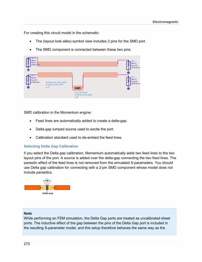
Electromagnetic
270
For creating this circuit model in the schematic:
• The (layout look-alike) symbol view includes 2 pins for the SMD port.
• The SMD component is connected between these two pins.
SMD calibration in the Momentum engine:
• Feed lines are automatically added to create a delta-gap.
• Delta-gap lumped source used to excite the port.
• Calibration standard used to de-embed the feed lines.
Selecting Delta Gap Calibration
if you select the Delta gap calibration, Momentum automatically adds two feed lines to the two layout pins of the port. A source is added over the delta-gap connecting the two feed lines. The parasitic effect of the feed lines is not removed from the simulated S-parameters. You should use Delta gap calibration for connecting with a 2-pin SMD component whose model does not include parasitics.
Note While performing an FEM simulation, the Delta Gap ports are treated as uncalibrated sheet ports. The inductive effect of the gap between the pins of the Delta Gap port is included in the resulting S-parameter model, and this setup therefore behaves the same way as the

271
Momentum Delta Gap source.
Defining Delta Gap Calibrated Ports 1. Choose EM > Simulation Setup to open the EM Setup window.
2. Select Ports in the left pane of the EM Setup window.
3. Select Delta Gap from the drop-list available in the Calibration column.
Momentum Source for Port with TML Calibration
In Momentum, there are two different lumped sources used in the TML calibration process to feed the circuits with calibration lines: a grounded source and a floating source. The grounded source works well for low frequencies, however at higher frequencies, when the port-ground distance becomes electrically large, this source provides less accurate results due to unwanted substrate coupling in the calibration process. The floating source works well at higher frequencies (unwanted substrate coupling is reduced), however it fails at low frequencies because the capacitive internal impedance of the source blocks the flow of the low frequency currents. The default behavior in Momentum is an automatic switching between these two sources, depending on the frequency range of the simulation.
The source type can be explicitly controlled using the following environment variable: MOM3D_USE_SOURCETYPE=0 (grounded, low frequency calibration source) MOM3D_USE_SOURCETYPE=1 (floating, high frequency calibration source)
This variable can be set in either of these locations: $HPEESOF_DIR/custom/config/momentum.cfg $HOME/hpeesof/config/momentum.cfg
In the ground reference, if multiple ports are excited with the same ground pin, the calibration should be set to None instead of TML. You cannot have two explicit TML ground reference ports (with same ground plane) on the same edge. In such cases, you should set the calibration to None.
5.1.7 Assigning Pins to an S-parameter Port
To assign a layout pin to the S-parameter port:
1. Choose EM > Simulation Setup to open the EM Setup window.

Electromagnetic
272
2. Select Ports in the left pane of the EM Setup window, as shown in the following figure:
3. Select a calibration type from the drop-list available in the Calibration column.
4. Select a pin row in Layout Pins. For example, P2 row is selected in the following figure:
5. Drag the pin from Layout Pins and drop it on the or terminal of the required port in S-parameter Ports. For example, P2 is dragged and dropped on the - terminal of Port1

273
in the following figure:
6. A message box is displayed if your target pin is already used by other ports.
7. Click Delete Ports and Continue in the message box.
Note You can drag and drop multiple layout pins and connect with a S-parameter port.
5.1.8 Using Edge and Area Pins in Ports
By default, Momentum uniformly injects current into the entire edge for port pins located on an edge. For pins located inside a polygon, Momentum injects current into a small area around the pin. You can precisely control the extent of this current injection using explicit Edge and Area pins. For more information, see Using Edge and Area Pins to learn how to create such pins.
A pin associated with a polyline or polygon shape needs to be properly positioned on that shape. Momentum will ignore the exact pin location and use the shape instead. The density of the injected current is then uniform over this edge or area shape.
FEM does not support area pins. Edge pins are supported when the edge is a line segment. Arcs and polylines with two or more segments are not supported. The precise location of the pin arrow will be used for the unsupported edge and area pins.
Fieldsets and LegendsSee Also
Setting up Ports Using Ports in Momentum Using Ports in FEM
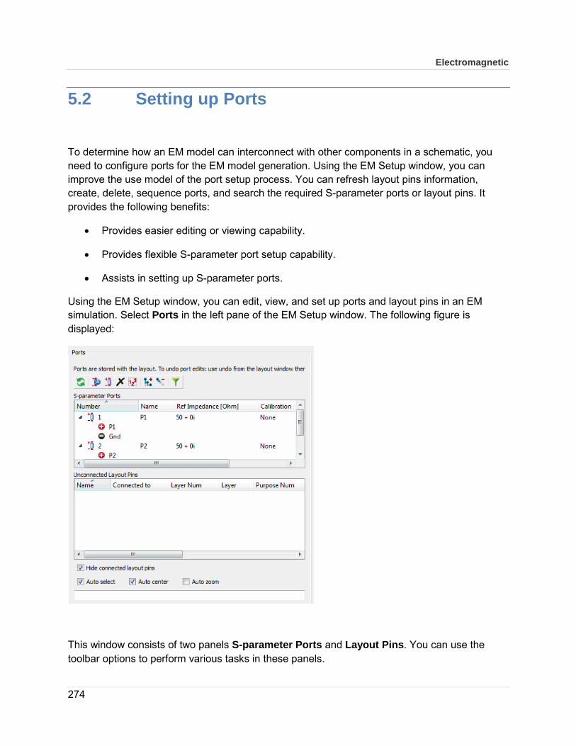
Electromagnetic
274
5.2 Setting up Ports
To determine how an EM model can interconnect with other components in a schematic, you need to configure ports for the EM model generation. Using the EM Setup window, you can improve the use model of the port setup process. You can refresh layout pins information, create, delete, sequence ports, and search the required S-parameter ports or layout pins. It provides the following benefits:
• Provides easier editing or viewing capability.
• Provides flexible S-parameter port setup capability.
• Assists in setting up S-parameter ports.
Using the EM Setup window, you can edit, view, and set up ports and layout pins in an EM simulation. Select Ports in the left pane of the EM Setup window. The following figure is displayed:
This window consists of two panels S-parameter Ports and Layout Pins. You can use the toolbar options to perform various tasks in these panels.
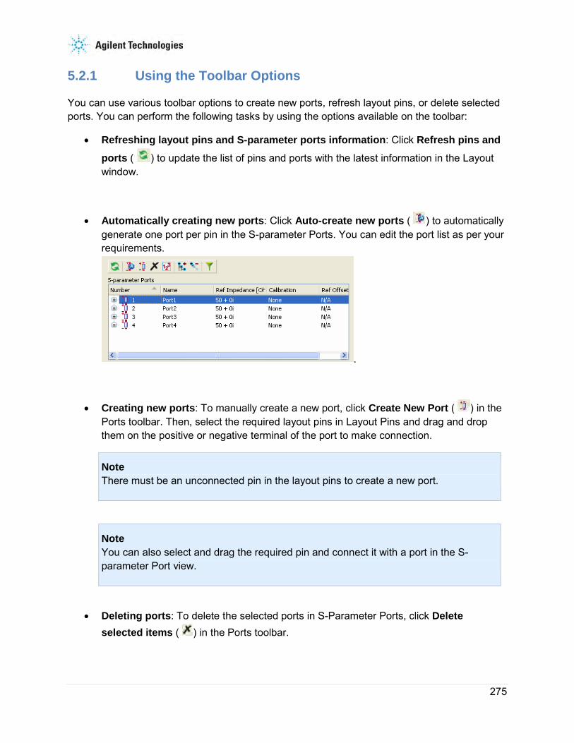
275
5.2.1 Using the Toolbar Options
You can use various toolbar options to create new ports, refresh layout pins, or delete selected ports. You can perform the following tasks by using the options available on the toolbar:
• Refreshing layout pins and S-parameter ports information: Click Refresh pins and
ports ( ) to update the list of pins and ports with the latest information in the Layout window.
• Automatically creating new ports: Click Auto-create new ports ( ) to automatically generate one port per pin in the S-parameter Ports. You can edit the port list as per your requirements.
.
• Creating new ports: To manually create a new port, click Create New Port ( ) in the Ports toolbar. Then, select the required layout pins in Layout Pins and drag and drop them on the positive or negative terminal of the port to make connection.
Note There must be an unconnected pin in the layout pins to create a new port.
Note You can also select and drag the required pin and connect it with a port in the S-parameter Port view.
• Deleting ports: To delete the selected ports in S-Parameter Ports, click Delete selected items ( ) in the Ports toolbar.

Electromagnetic
276
Note The port number will always be retained in sequence.
• Resequencing ports: Click Resequence Ports ( ) to open the Reorder Port Numbers window.
From the Reorder Port Numbers window, select the required port and click the Up and Down keys to change the ports sequence according to your requirements.
• Expanding S-parameter ports tree: To display the detailed information about each port in S-Parameter Ports, click Expand S-parameter Ports tree ( ).
• Collapsing S-parameter ports tree: To hide the details of ports in S-Parameter Ports, click Collapse S-parameter Ports tree ( ).
• Searching the required information: For easy filtering and sorting commands, click Toggle Search Filter On/Off ( ). Type the required string in the Search text box. In the Layout Pins panel, you can also right-click any required field and select Set texts to filter. This option picks up the text of current item in Layout Pins and sets it in the filter,
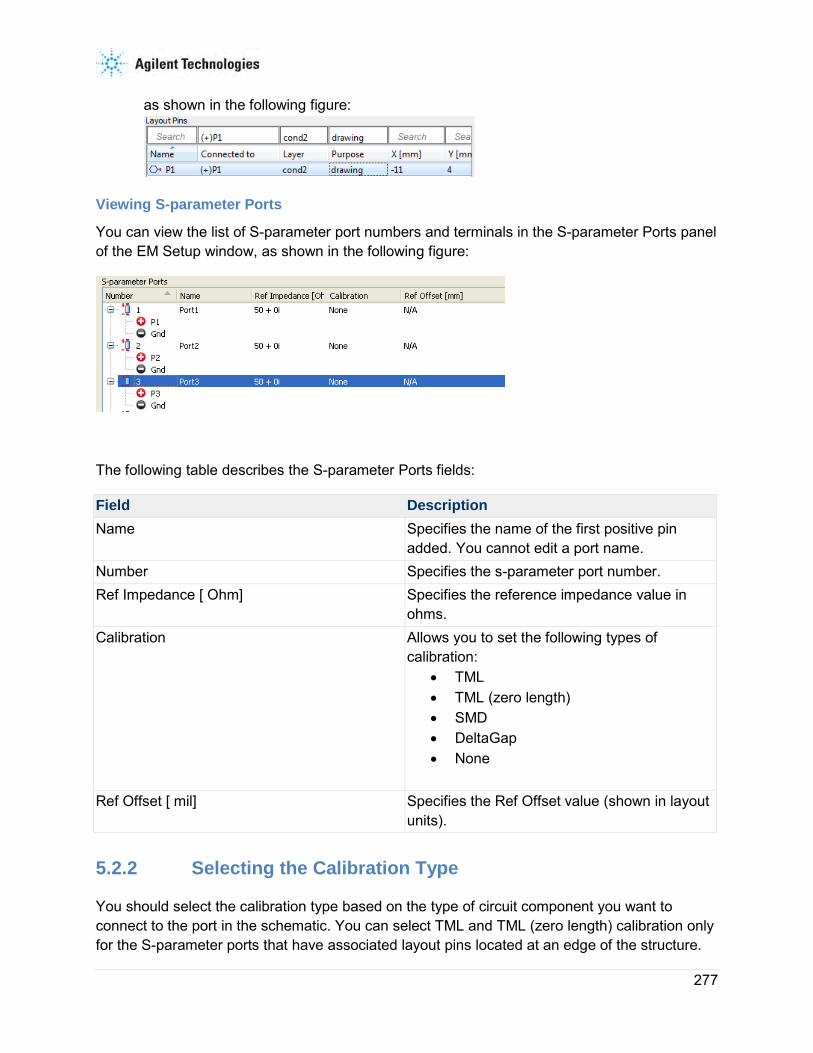
277
as shown in the following figure:
Viewing S-parameter Ports
You can view the list of S-parameter port numbers and terminals in the S-parameter Ports panel of the EM Setup window, as shown in the following figure:
The following table describes the S-parameter Ports fields:
Field Description Name Specifies the name of the first positive pin
added. You cannot edit a port name. Number Specifies the s-parameter port number. Ref Impedance [ Ohm] Specifies the reference impedance value in
ohms. Calibration Allows you to set the following types of
calibration: • TML • TML (zero length) • SMD • DeltaGap • None
Ref Offset [ mil] Specifies the Ref Offset value (shown in layout
units).
5.2.2 Selecting the Calibration Type
You should select the calibration type based on the type of circuit component you want to connect to the port in the schematic. You can select TML and TML (zero length) calibration only for the S-parameter ports that have associated layout pins located at an edge of the structure.

Electromagnetic
278
You can select SMD and Delta gap only for S-parameters ports that have two associated layout pins located at the edges of a gap in the structure. For S-parameter ports which have at least one associated layout pin inside the structure, None is the only option that can be selected as calibration type. Depending on your circuit component, you can select the following types of calibration:
• TML: Connects a transmission line component.
• TML(zero length): Connects a lumped component.
• SMD: Connects a 2-pin SMD component (model includes parasitics).
• Delta gap: Connects a 2-pin SMD component (model does not include parasitics).
• None: If none of the available calibration types is valid for the connecting component, specify None.
5.2.3 Selecting the S-Parameter Ports Title Fields
You can select the required heading fields in S-parameter Ports by performing the following steps:
1. Right-click the title bar and then select View Option. This opens the View Option dialog box, as shown in the following figure:
2. Select the required fields.
3. Click OK.
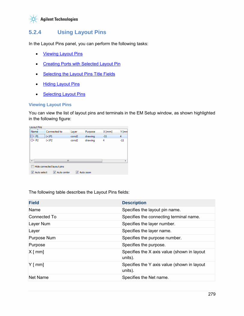
279
5.2.4 Using Layout Pins
In the Layout Pins panel, you can perform the following tasks:
• Viewing Layout Pins
• Creating Ports with Selected Layout Pin
• Selecting the Layout Pins Title Fields
• Hiding Layout Pins
• Selecting Layout Pins
Viewing Layout Pins
You can view the list of layout pins and terminals in the EM Setup window, as shown highlighted in the following figure:
The following table describes the Layout Pins fields:
Field Description Name Specifies the layout pin name. Connected To Specifies the connecting terminal name. Layer Num Specifies the layer number. Layer Specifies the layer name. Purpose Num Specifies the purpose number. Purpose Specifies the purpose. X [ mm] Specifies the X axis value (shown in layout
units). Y [ mm] Specifies the Y axis value (shown in layout
units). Net Name Specifies the Net name.

Electromagnetic
280
Field Description Number Specifies the number. Pin Type Specifies the type of pin used in the design.
Creating Ports with Selected Layout Pin
In the Layout pins panel, you can create port in the following ways:
• Creating a port with selected pins: Right-click the required layout pin and select Create Ports. It creates a port with the selected layout pin.
• Creating a port with clustering pins: Right-click the required layout pin and select Create a Port with clustering pins. It creates a port with all selected layout pins for the plus pin of a S-parameter port.
Selecting the Layout Pins Title Fields
You can select the required heading fields in Layout Pins by performing the following steps:
1. Right-click the title bar and select View Option. This opens the View Option dialog box, as shown in the following figure:
Note The Tool-related parameters such as Name (from Tool) are available only when the pins are imported through Allegro DFI. Otherwise, these parameters are shown as N/A, if you try to select in the View Option dialog box.
2. Select the required fields.
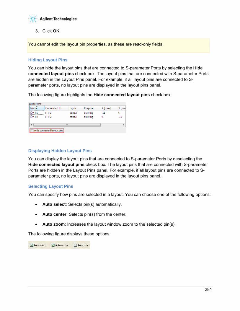
281
3. Click OK.
You cannot edit the layout pin properties, as these are read-only fields.
Hiding Layout Pins
You can hide the layout pins that are connected to S-parameter Ports by selecting the Hide connected layout pins check box. The layout pins that are connected with S-parameter Ports are hidden in the Layout Pins panel. For example, if all layout pins are connected to S-parameter ports, no layout pins are displayed in the layout pins panel.
The following figure highlights the Hide connected layout pins check box:
Displaying Hidden Layout Pins
You can display the layout pins that are connected to S-parameter Ports by deselecting the Hide connected layout pins check box. The layout pins that are connected with S-parameter Ports are hidden in the Layout Pins panel. For example, if all layout pins are connected to S-parameter ports, no layout pins are displayed in the layout pins panel.
Selecting Layout Pins
You can specify how pins are selected in a layout. You can choose one of the following options:
• Auto select: Selects pin(s) automatically.
• Auto center: Selects pin(s) from the center.
• Auto zoom: Increases the layout window zoom to the selected pin(s).
The following figure displays these options:
Electromagnetic
282
5.3 Using Ports in Momentum This section provides information about the following topics:
• Momentum Ports Overview
• Using Calibrated Ports
• Using Uncalibrated Ports
5.3.1 Momentum Ports Overview
One of the most intimidating, challenging, and confusing topics to master for electromagnetic (EM) simulations is that of exciting a given design with the most accurate representation of what one would use when testing a component or module in a lab environment. Most EM tools refer to these excitations as ports. This section lists various ports available in ADS and the appropriate methods to define and apply them.
You can use the following calibration types:
• TML: Connects a transmission line component.
• TML(zero length): Connects a lumped component.
• SMD: Connects a 2-pin SMD component (model includes parasitics).
• Delta gap: Connects a 2-pin SMD component (model does not include parasitics).
• None: If none of the available calibration types is valid for the connecting component, specify None. It is useful for making a connection with lumped elements or for representing other connections in the circuit.
Using the EM Setup window, you can edit, view, and set up ports and layout pins in an EM simulation. Select Ports in the left pane of the EM Setup window. This window consists of two panels S-parameter Ports and Layout Pins. You can use the toolbar options to perform various tasks in these panels.
• Layout Pin: Specifies a location in layout, either edge or area.
• S-parameter Port: Specifies a circuit port connecting two Layout Pins
The following figure displays an EM Setup window:
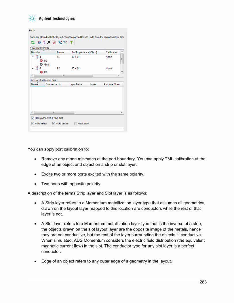
283
You can apply port calibration to:
• Remove any mode mismatch at the port boundary. You can apply TML calibration at the edge of an object and object on a strip or slot layer.
• Excite two or more ports excited with the same polarity.
• Two ports with opposite polarity.
A description of the terms Strip layer and Slot layer is as follows:
• A Strip layer refers to a Momentum metallization layer type that assumes all geometries drawn on the layout layer mapped to this location are conductors while the rest of that layer is not.
• A Slot layer refers to a Momentum metallization layer type that is the inverse of a strip, the objects drawn on the slot layout layer are the opposite image of the metals, hence they are not conductive, but the rest of the layer surrounding the objects is conductive. When simulated, ADS Momentum considers the electric field distribution (the equivalent magnetic current flow) in the slot. The conductor type for any slot layer is a perfect conductor.
• Edge of an object refers to any outer edge of a geometry in the layout.
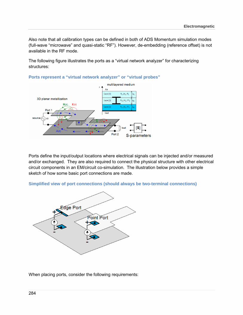
Electromagnetic
284
Also note that all calibration types can be defined in both of ADS Momentum simulation modes (full-wave “microwave” and quasi-static “RF”). However, de-embedding (reference offset) is not available in the RF mode.
The following figure illustrates the ports as a “virtual network analyzer” for characterizing structures:
Ports represent a “virtual network analyzer” or “virtual probes”
Ports define the input/output locations where electrical signals can be injected and/or measured and/or exchanged. They are also required to connect the physical structure with other electrical circuit components in an EM/circuit co-simulation. The illustration below provides a simple sketch of how some basic port connections are made.
Simplified view of port connections (should always be two-terminal connections)
When placing ports, consider the following requirements:

285
• Ports should have two terminals (signal +, ground -). Often, the ground terminal is implicitly defined.
• Each terminal should be at a unique potential. This means that ports should not be placed on electrically long edges.
• The distance between two terminals is lumped. In this context, “lumped” means “electrically small” (size < /10), which implies no phase delay between + and - terminal.
• Violating one of the above requirements can yield unphysical results.
In the EM space, the following fundamental fields are modeled:
• Electric field, E(r)
• Magnetic field, H(r)
These fields are derived from the following potentials:
• Magnetic vector potential, A(r)
• Electric scalar potential, V(r)
The scalar potential V(r) at infinity (r = ) is zero, V( )=0. The zero potential at infinity is also referred as as “Ground at Infinity”.
In the circuit space, models are described by ports with:
• Voltage (Vp)
• Current (Ip) Where ports have two terminals: + signal and - reference. In Momentum, the port voltage is defined as the difference of the electric scalar potential between the two terminals: Vp = V(r+) - V(r-)
While the + terminal is always explicitly defined with either a calibrated or uncalibrated port, the - terminal can be defined in a few ways:
• When there is an infinite ground plane, the - terminal is implicitly located in the infinite ground plane closest to the + terminal.
• In the absence of an infinite ground plane, the - terminal (called ground ref port, a potentially confusing name) needs to be explicitly defined somewhere close to the + terminal.
• When there is no - terminal and no infinite ground plane, port voltage for uncalibrated ports is defined as the value of the electric scalar potential at the + terminal:
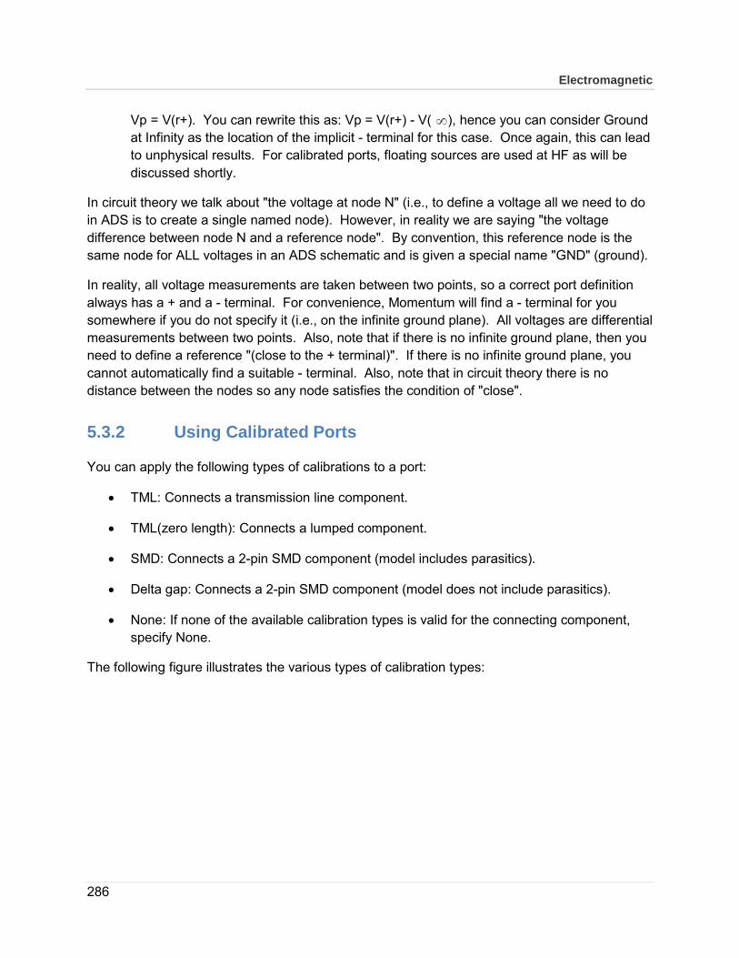
Electromagnetic
286
Vp = V(r+). You can rewrite this as: Vp = V(r+) - V( ), hence you can consider Ground at Infinity as the location of the implicit - terminal for this case. Once again, this can lead to unphysical results. For calibrated ports, floating sources are used at HF as will be discussed shortly.
In circuit theory we talk about "the voltage at node N" (i.e., to define a voltage all we need to do in ADS is to create a single named node). However, in reality we are saying "the voltage difference between node N and a reference node". By convention, this reference node is the same node for ALL voltages in an ADS schematic and is given a special name "GND" (ground).
In reality, all voltage measurements are taken between two points, so a correct port definition always has a + and a - terminal. For convenience, Momentum will find a - terminal for you somewhere if you do not specify it (i.e., on the infinite ground plane). All voltages are differential measurements between two points. Also, note that if there is no infinite ground plane, then you need to define a reference "(close to the + terminal)". If there is no infinite ground plane, you cannot automatically find a suitable - terminal. Also, note that in circuit theory there is no distance between the nodes so any node satisfies the condition of "close".
5.3.2 Using Calibrated Ports
You can apply the following types of calibrations to a port:
• TML: Connects a transmission line component.
• TML(zero length): Connects a lumped component.
• SMD: Connects a 2-pin SMD component (model includes parasitics).
• Delta gap: Connects a 2-pin SMD component (model does not include parasitics).
• None: If none of the available calibration types is valid for the connecting component, specify None.
The following figure illustrates the various types of calibration types:

287
Th following sections provide information about the calibrated port types available in Momentum and also provides explanations on their influence on simulation results.
Excitation Sources for Calibrated Ports
Sources are needed to excite the structures at the ports. Momentum use two types of sources, grounded and floating, to excite calibrated ports. These simulators automatically uses a grounded source below the quasi-static frequency and a floating source above the quasi-static frequency (fqs). The quasi-static frequency is chosen automatically by Momentum such that it lies in the range fmin-fmax and is qualitatively the frequency at which the accuracy of low-frequency (i.e., electrically small) approximations begins to decay as the frequency increases. The grounded source becomes unphysical at high frequencies (electrically long), while the floating source becomes unstable at low frequencies (block's the DC current). These simulators switches between source types at the quasi-static frequencies to avoid these issues.
Frequency ranges for which grounded sources and floating sources are used
For the grounded (low-frequency) source, consider the following factors:
• This source is used in Momentum RF for all frequencies.
• This source is used in Momentum MW at low frequencies (below ~10 MHz, the exact transition frequency is substrate dependent).
• This source is a grounded source (connected between the port and the ground). The + terminal is connected to port and the - terminal connected to ground below port.
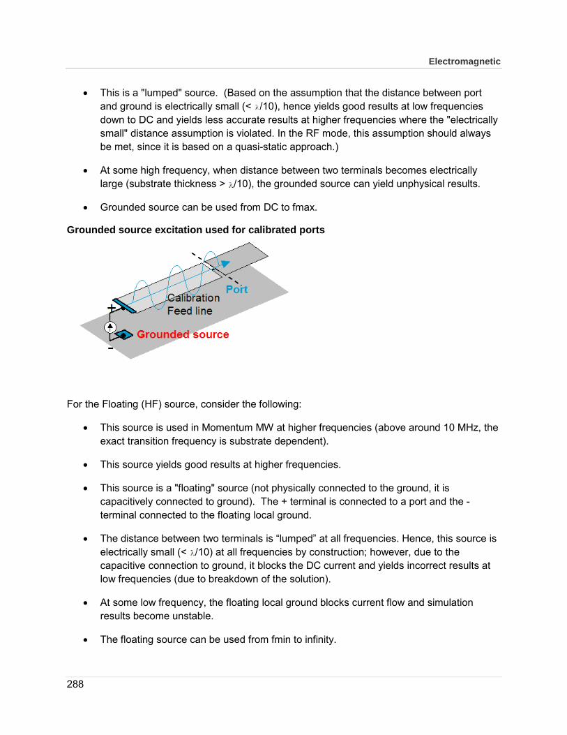
Electromagnetic
288
• This is a "lumped" source. (Based on the assumption that the distance between port and ground is electrically small (< /10), hence yields good results at low frequencies down to DC and yields less accurate results at higher frequencies where the "electrically small" distance assumption is violated. In the RF mode, this assumption should always be met, since it is based on a quasi-static approach.)
• At some high frequency, when distance between two terminals becomes electrically large (substrate thickness > /10), the grounded source can yield unphysical results.
• Grounded source can be used from DC to fmax.
Grounded source excitation used for calibrated ports
For the Floating (HF) source, consider the following:
• This source is used in Momentum MW at higher frequencies (above around 10 MHz, the exact transition frequency is substrate dependent).
• This source yields good results at higher frequencies.
• This source is a "floating" source (not physically connected to the ground, it is capacitively connected to ground). The + terminal is connected to a port and the - terminal connected to the floating local ground.
• The distance between two terminals is “lumped” at all frequencies. Hence, this source is electrically small (< /10) at all frequencies by construction; however, due to the capacitive connection to ground, it blocks the DC current and yields incorrect results at low frequencies (due to breakdown of the solution).
• At some low frequency, the floating local ground blocks current flow and simulation results become unstable.
• The floating source can be used from fmin to infinity.

289
Floating source excitation used for calibrated ports
The transition between the LF and HF source in Momentum MW is set at a frequency that is substrate dependent, typically around 1 to 10 MHz, where both the LF and the HF source are valid sources, hence, the S-parameters obtained by using either sources should be identical and the transition can be made safely. In some cases, the transition happens at too low frequency and you see the incorrect results of the solution breakdown caused by the HF sources. You can control the use of the source by setting the following config variable MOM3D_USE_SOURCETYPE in the momentum.cfg file:
• MOM3D_USE_SOURCETYPE=0 forces the use of the grounded LF source at all frequencies.
• MOM3D_USE_SOURCETYPE=1 forces the use of the floating HF source at all frequencies. For cases when the transition is not smooth between the two models, the grounded low-frequency source should yield consistent results.
Applying TML Calibration
The Transmission Line Calibration (TML) technique is used in Momentum for TML port positive pin, common, and differential ports.
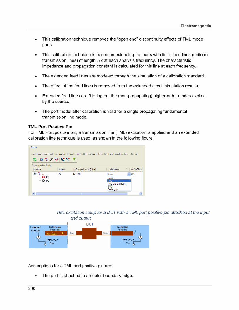
Electromagnetic
290
• This calibration technique removes the “open end” discontinuity effects of TML mode ports.
• This calibration technique is based on extending the ports with finite feed lines (uniform transmission lines) of length /2 at each analysis frequency. The characteristic impedance and propagation constant is calculated for this line at each frequency.
• The extended feed lines are modeled through the simulation of a calibration standard.
• The effect of the feed lines is removed from the extended circuit simulation results.
• Extended feed lines are filtering out the (non-propagating) higher-order modes excited by the source.
• The port model after calibration is valid for a single propagating fundamental transmission line mode.
TML Port Positive Pin For TML Port positive pin, a transmission line (TML) excitation is applied and an extended calibration line technique is used, as shown in the following figure:
TML excitation setup for a DUT with a TML port positive pin attached at the input and output
Assumptions for a TML port positive pin are:
• The port is attached to an outer boundary edge.
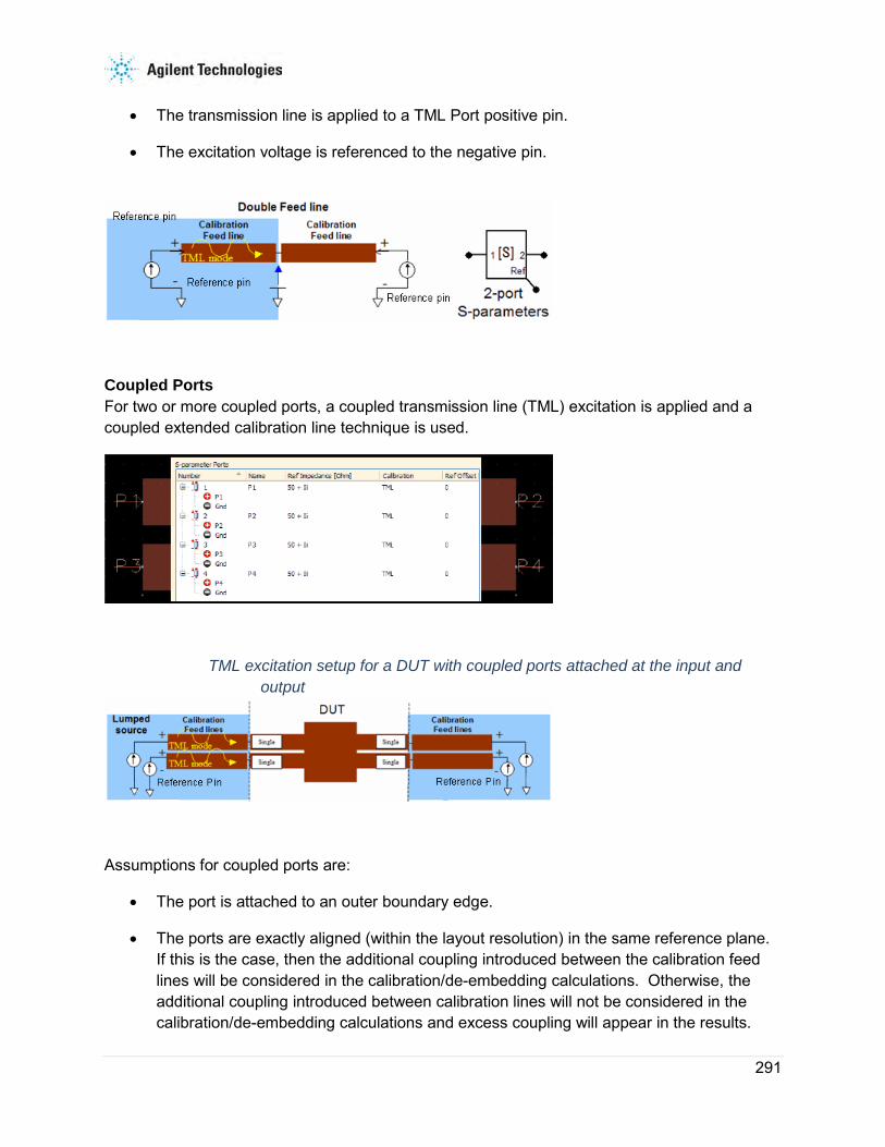
291
• The transmission line is applied to a TML Port positive pin.
• The excitation voltage is referenced to the negative pin.
Coupled Ports For two or more coupled ports, a coupled transmission line (TML) excitation is applied and a coupled extended calibration line technique is used.
TML excitation setup for a DUT with coupled ports attached at the input and output
Assumptions for coupled ports are:
• The port is attached to an outer boundary edge.
• The ports are exactly aligned (within the layout resolution) in the same reference plane. If this is the case, then the additional coupling introduced between the calibration feed lines will be considered in the calibration/de-embedding calculations. Otherwise, the additional coupling introduced between calibration lines will not be considered in the calibration/de-embedding calculations and excess coupling will appear in the results.
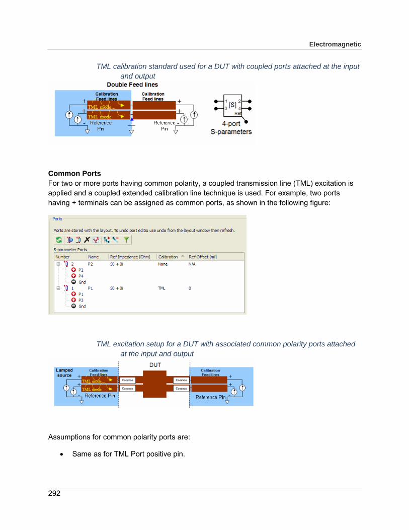
Electromagnetic
292
TML calibration standard used for a DUT with coupled ports attached at the input and output
Common Ports For two or more ports having common polarity, a coupled transmission line (TML) excitation is applied and a coupled extended calibration line technique is used. For example, two ports having + terminals can be assigned as common ports, as shown in the following figure:
TML excitation setup for a DUT with associated common polarity ports attached at the input and output
Assumptions for common polarity ports are:
• Same as for TML Port positive pin.

293
• The ports are aligned in the same reference plane and are desired to be considered as same-polarity (common-mode) combined ports.
The following figure displays the calibration standard used for structures with common ports in the following figure:
From this, the calibrated and recombined S-parameters can be calculated.
Differential Ports For a pair of differential ports, a coupled transmission line (TML) excitation is applied and a coupled extended calibration line technique is used.
TML excitation setup for a DUT with associated differential ports attached at the input and output
Assumptions for differential ports are:

Electromagnetic
294
• Same as for TML Port positive pin.
• The ports are aligned in the same reference plane and are desired to be considered as opposite-polarity (differential-mode) combined ports.
Reference Pins Associated with TML Port Positive Pin For reference pins associated with TML port positive pin, a TML excitation is applied and a coupled extended calibration line technique is used. Also, local ground recombination and grouping is applied to the associated ports.
The TML excitation setup for a DUT with reference pins associated with a TML port positive pin attached at the input and output
Assumptions:
• Same as for TML Port positive pin.
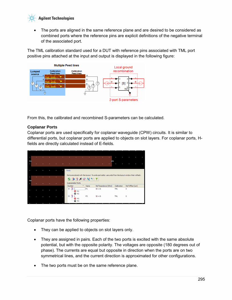
295
• The ports are aligned in the same reference plane and are desired to be considered as combined ports where the reference pins are explicit definitions of the negative terminal of the associated port.
The TML calibration standard used for a DUT with reference pins associated with TML port positive pins attached at the input and output is displayed in the following figure:
From this, the calibrated and recombined S-parameters can be calculated.
Coplanar Ports Coplanar ports are used specifically for coplanar waveguide (CPW) circuits. It is similar to differential ports, but coplanar ports are applied to objects on slot layers. For coplanar ports, H-fields are directly calculated instead of E-fields.
Coplanar ports have the following properties:
• They can be applied to objects on slot layers only.
• They are assigned in pairs. Each of the two ports is excited with the same absolute potential, but with the opposite polarity. The voltages are opposite (180 degrees out of phase). The currents are equal but opposite in direction when the ports are on two symmetrical lines, and the current direction is approximated for other configurations.
• The two ports must be on the same reference plane.
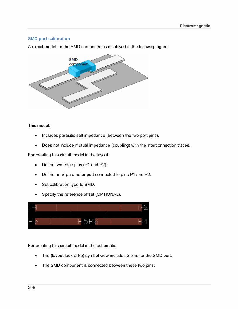
Electromagnetic
296
SMD port calibration
A circuit model for the SMD component is displayed in the following figure:
This model:
• Includes parasitic self impedance (between the two port pins).
• Does not include mutual impedance (coupling) with the interconnection traces.
For creating this circuit model in the layout:
• Define two edge pins (P1 and P2).
• Define an S-parameter port connected to pins P1 and P2.
• Set calibration type to SMD.
• Specify the reference offset (OPTIONAL).
For creating this circuit model in the schematic:
• The (layout look-alike) symbol view includes 2 pins for the SMD port.
• The SMD component is connected between these two pins.

297
SMD calibration in the Momentum engine:
• Feed lines are automatically added to create a delta-gap.
• Delta-gap lumped source used to excite the port.
• Calibration standard used to de-embed the feed lines.
Assessment of calibration accuracy Simulation with SMD replaced by matching line section should give SAME result as simulation of straight line without SMD ports
Perfectly calibrated means these two simulations give identical results

Electromagnetic
298
SMD circuit component parasitic self impedance included mutual impedance NOT included
SMD port calibration:
• Feed lines with delta-gap source
• Includes self and mutual impedance
• SMD calibration removes the parasitic self impedance (NOT the mutual impedance)
• Reference shift can be used to control amount of self impedance removed

299
Using Delta Gap port calibration
In this section, a physical structure is connected with a Delta Gap component. Assumptions for the circuit model for the Delta Gap component:
• Does NOT include parasitic self impedance (between the two port pins).
• Does NOT include mutual impedance (coupling) with the interconnection traces taken into account through DeltaGap port calibration.
• User defines two edge pins (P1 and P2).
• User defines an S-parameter port connected to pins P1 and P2.
• User sets calibration type to DeltaGap.
The following Use Model is used in in schematic:
• The (layout look-alike) symbol view includes 2 pins for the DeltaGap port.
• The SMD component is connected between these two pins.

Electromagnetic
300
DeltaGap calibration in the Momentum Engine:
• Feed lines are automatically added to create a delta-gap
• Delta-gap lumped source used to excite the port
Assessment of calibration accuracy
Simulation with very small (delta) gap in layout with NO calibration gives SAME result as simulation of physical SMD gap with DeltaGap calibration.
5.3.3 Using Uncalibrated Ports
If none of the available calibration types is valid for a connecting component, the port is uncalibrated. Select the None calibration in the EM Setup window. ADS allows you to define direct excitation by creating uncalibrated ports. These ports can be specified at any location on the planar metallization patterns as either a line feed or a point feed. Uncalibrated ports allow the connection of both passive and active lumped components to the distributed model of the planar circuits calculated by Momentum. The point feed port provides a way to model the connection with surface mounted components or bond wires.
In ADS, any negative – pin can serve as a reference pin, whether it is a local potential/voltage reference or a global ground. An uncalibrated port connected between a + pin and a - pin is considered to excite the structure in a differential way. The – pin is just a reference point for the excitation port. The S-parameters associated with uncalibrated ports are calculated by exciting the circuit with a lumped voltage source connected to the branches in the equivalent LC network corresponding with the port edges in the mesh.
Note for uncalibrated ports associated with reference pins: ADS uses a lumped voltage source to excite the circuit at the uncalibrated port + pin and reference - pin combinations. Lumped implies that the distance between + pin and - pin is electrically small (< /10) at all frequencies. Users are not prohibited by the EM Setup window to define uncalibrated ports associated with reference pin that do not follow this rule and can get unphysical simulation data as a result.
For uncalibrated ports, a lumped source excitation is applied and no calibration technique is used. The following figure displays the source excitation used for uncalibrated ports, which applies to both edge ports (shown on left) and to point ports (shown on right).
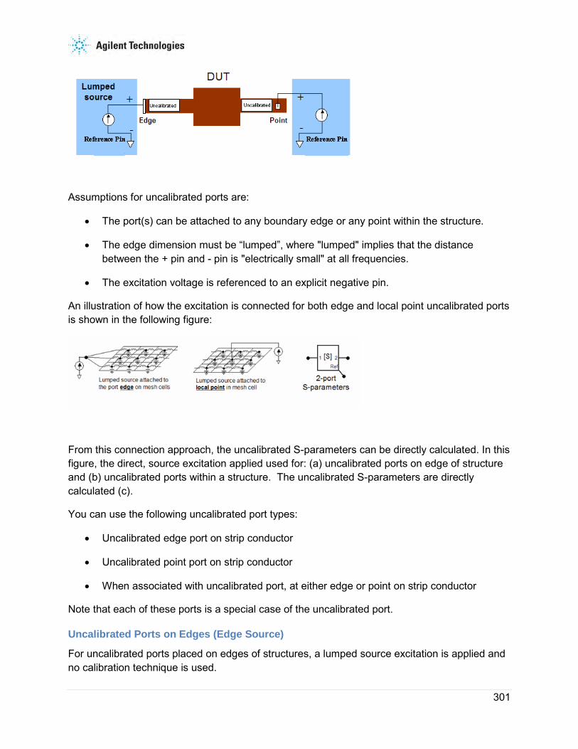
301
Assumptions for uncalibrated ports are:
• The port(s) can be attached to any boundary edge or any point within the structure.
• The edge dimension must be “lumped”, where "lumped" implies that the distance between the + pin and - pin is "electrically small" at all frequencies.
• The excitation voltage is referenced to an explicit negative pin.
An illustration of how the excitation is connected for both edge and local point uncalibrated ports is shown in the following figure:
From this connection approach, the uncalibrated S-parameters can be directly calculated. In this figure, the direct, source excitation applied used for: (a) uncalibrated ports on edge of structure and (b) uncalibrated ports within a structure. The uncalibrated S-parameters are directly calculated (c).
You can use the following uncalibrated port types:
• Uncalibrated edge port on strip conductor
• Uncalibrated point port on strip conductor
• When associated with uncalibrated port, at either edge or point on strip conductor
Note that each of these ports is a special case of the uncalibrated port.
Uncalibrated Ports on Edges (Edge Source)
For uncalibrated ports placed on edges of structures, a lumped source excitation is applied and no calibration technique is used.

Electromagnetic
302
Assumptions for uncalibrated ports connected to geometry edges are:
• The port(s) can be attached to any boundary edge in the layout.
• The edge dimension should be lumped, where "lumped" implies that the distance between the + pin and - pin is "electrically small" at all frequencies.
• The excitation voltage is referenced to the explicit negative pin.
An illustration of how the excitation is connected for the edge uncalibrated ports is shown below. From this connection approach, the uncalibrated S-parameters can be directly calculated.
When placing an uncalibrated edge ports on any edge of a geometry in layout, the port is connected to all of the edges of the mesh cells defined at that geometry edge. In the example shown above, there are 3 mesh edges affected by the edge port. The sum of the currents through the port edges make up the port current. The voltage of the lumped voltage source attached to the port is distributed over the three port edges in the layout.
Note that the distribution of the applied port voltage over more than one edge in the mesh can cause a problem if the edge that the port is attached to is significantly wider than a mesh cell. This occurs since the port edges are short circuited when the “Internal” port is left open. These short-circuited port edges introduce extra loops in the equivalent circuit, which is hereby different than the equivalent circuit without “Internal” ports.
Graphic representation of extra current loops that can be created when the lumped excitation applied for Internal edge ports is applied over a wide geometry edge. Graphic representation of extra current loops that can be created when the lumped excitation applied for Internal edge ports is applied over a wide geometry edge.

303
To resolve this problem for uncalibrated edge-fed ports on wide edges, you should ensure that there is only one edge in the mesh associated with the uncalibrated port. This is accomplished by attaching the uncalibrated port to a very small rectangle (of insignificant length) added to the layout. In this case, no extra loops are introduced in the equivalent circuit and the simulation results with open uncalibrated ports are the same as the results without uncalibrated ports.
Using Edge and Area Pins in Ports By default, Momentum uniformly injects current into the entire edge for port pins located on an edge. For pins located inside a polygon, Momentum injects current into a small area around the pin. You can precisely control the extent of this current injection using explicit Edge and Area pins. A pin associated with a polyline or polygon shape needs to be properly positioned on that shape. Momentum will ignore the exact pin location and use the shape instead. The density of the injected current is then uniform over this edge or area shape. If you want to apply an uncalibrated edge port to a wide geometry edges, you should add a very small rectangle to that edge in order to minimize non-physical effects. It is a legacy approach that is supported in ADS 2009 and older ADS versions. From ADS 2011 release onwards, the new edge pin enhanced capability is supported. Both edge and area pins are supported by uncalibrated ports defined inside structures.
The small piece of extra metallization lends to a cleaner excitation for wide geometry edges.
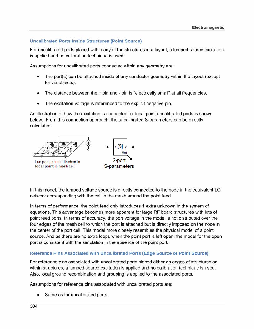
Electromagnetic
304
Uncalibrated Ports Inside Structures (Point Source)
For uncalibrated ports placed within any of the structures in a layout, a lumped source excitation is applied and no calibration technique is used.
Assumptions for uncalibrated ports connected within any geometry are:
• The port(s) can be attached inside of any conductor geometry within the layout (except for via objects).
• The distance between the + pin and - pin is "electrically small" at all frequencies.
• The excitation voltage is referenced to the explicit negative pin.
An illustration of how the excitation is connected for local point uncalibrated ports is shown below. From this connection approach, the uncalibrated S-parameters can be directly calculated.
In this model, the lumped voltage source is directly connected to the node in the equivalent LC network corresponding with the cell in the mesh around the point feed.
In terms of performance, the point feed only introduces 1 extra unknown in the system of equations. This advantage becomes more apparent for large RF board structures with lots of point feed ports. In terms of accuracy, the port voltage in the model is not distributed over the four edges of the mesh cell to which the port is attached but is directly imposed on the node in the center of the port cell. This model more closely resembles the physical model of a point source. And as there are no extra loops when the point port is left open, the model for the open port is consistent with the simulation in the absence of the point port.
Reference Pins Associated with Uncalibrated Ports (Edge Source or Point Source)
For reference pins associated with uncalibrated ports placed either on edges of structures or within structures, a lumped source excitation is applied and no calibration technique is used. Also, local ground recombination and grouping is applied to the associated ports.
Assumptions for reference pins associated with uncalibrated ports are:
• Same as for uncalibrated ports.
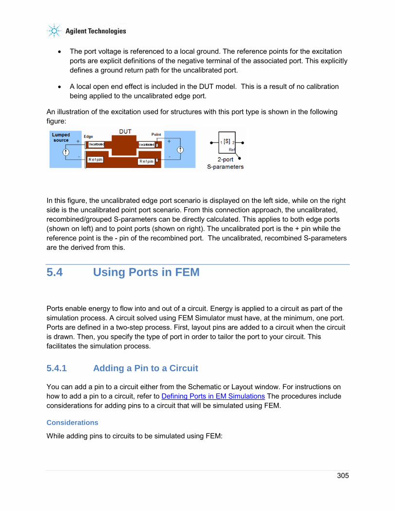
305
• The port voltage is referenced to a local ground. The reference points for the excitation ports are explicit definitions of the negative terminal of the associated port. This explicitly defines a ground return path for the uncalibrated port.
• A local open end effect is included in the DUT model. This is a result of no calibration being applied to the uncalibrated edge port.
An illustration of the excitation used for structures with this port type is shown in the following figure:
In this figure, the uncalibrated edge port scenario is displayed on the left side, while on the right side is the uncalibrated point port scenario. From this connection approach, the uncalibrated, recombined/grouped S-parameters can be directly calculated. This applies to both edge ports (shown on left) and to point ports (shown on right). The uncalibrated port is the + pin while the reference point is the - pin of the recombined port. The uncalibrated, recombined S-parameters are the derived from this.
5.4 Using Ports in FEM
Ports enable energy to flow into and out of a circuit. Energy is applied to a circuit as part of the simulation process. A circuit solved using FEM Simulator must have, at the minimum, one port. Ports are defined in a two-step process. First, layout pins are added to a circuit when the circuit is drawn. Then, you specify the type of port in order to tailor the port to your circuit. This facilitates the simulation process.
5.4.1 Adding a Pin to a Circuit
You can add a pin to a circuit either from the Schematic or Layout window. For instructions on how to add a pin to a circuit, refer to Defining Ports in EM Simulations The procedures include considerations for adding pins to a circuit that will be simulated using FEM.
Considerations
While adding pins to circuits to be simulated using FEM:

Electromagnetic
306
• The components or shapes that pins are connected to must be on layout layers that are mapped to metallization layers that are defined as strips or slots. Pins cannot be directly connected to vias.
• Make sure that pins on edges are positioned so that the arrow is outside of the object, pointing inwards, and at a straight angle.
• Make sure that the pin and the object you are connecting it to are on the same layout layer. For convenience, you can set the entry layer to this layer; the Entry Layer listbox is on the Layout tool bar.
• A pin must be applied to an object. If a pin is applied in open space so that it is not connected to an object, Momentum will automatically snap the pin to the edge of the closest object. However, the FEM Simulator will leave the pin unattached to the structure. This difference will not be apparent from the layout, however, because the position of the pin will not change.
5.4.2 Selecting the Port Calibration
FEM supports TML and None port calibration. If you do not assign port calibration type, a port in the circuit is treated as a None port type during simulation.
5.4.3 Defining a TML Port Calibration
TML port calibration is the default port type. It has the following properties:
• It is connected to an object that is on either a strip or slot metallization layer.
• It can be applied only to the edge of an object.
• The port is external and calibrated. The port is excited using a calibration process that removes any undesired reactive effects of the port excitations (mode mismatch) at the port boundary.

307
• FEM Simulator requires single ports to be on a TML port calibration that surrounds the circuit. Ports that are not on this bounding box will be treated as None calibrated ports.
• The port boundary can be moved into or away from the geometry by specifying a reference offset. S-parameters will be calculated as if the port were at this position. For more information, refer to Applying Reference Offsets.
• If the port is connected to an object that is on a slot layer, the port has polarity.
Hint TML is the default calibration type, but it will revert to None if not on the bounding. Any port without a port type specified is assumed to be a TML port.
To define a TML port calibration:
1. Choose EM > Simulation Setup to open the EM Setup window.
2. Select FEM.
3. Select Ports in the left pane of the EM Setup window.
4. Select TML in the Calibration column.
FEM uses the Waveguide ports or TML calibration to shift the location of the reference lines used for the S-parameters. It consists of the following features:
• Calibrated 2D-plane source
• User defines a 2D plane for the port in the simulation domain with a source impedance, which could be simply 50? or RLC
• Higher order modes calculations are available
You can select the following types of reference offsets:

Electromagnetic
308
• Specifying a positive reference offset: Shifts the reference planes in the direction towards the circuit.
• Specifying a negative reference offset: Shifts the reference planes in the direction away from the circuit.
5.4.4 Defining the None Port Calibration
The None port calibration enables you to apply a port to the surface of an object in your design. By using None calibration, all the physical connections in a circuit can be represented, so your simulation can take into account all of the EM coupling effects that will occur among ports in the circuit. These coupling effects caused by parasitics are included in your simulation results because ports are not calibrated. You should avoid geometries that allow coupling between TML and None calibrated ports to prevent incorrect S-parameters.
An example of where an internal None port is necessary is a circuit that consists of transmission lines that connect to a device, such as a transistor or a chip capacitor, but this device is not part of the circuit that you are simulating. An internal None port can be placed at the connection point, so even though the device is not part of the circuit you are simulating, the coupling effects that occur among the ports and around the device will be included in your simulation.
A None calibrated port has the following properties:
• None ports that are connected to either a geometry edge or are connected to an internal edge created with a polyline to create an edge pin will be implemented as sheet ports.
• It can be applied to the interior of a circuit by applying it to the surface of an object.
• It can be applied to the edge of an object.
• It can be applied to objects that are on strip layers only.
• The orientation of the port is not considered if it is on the surface of an object.
• No calibration is performed on the port.
FEM uses None Calibration Ports (which are essentially Voltage source Ports) to inject energy into a structure as an alternative to ports. Sources are useful for modeling internal ports within a structure. Some examples are:
• Your structure consists of transmission lines that connect to a device, such as a transistor, but this device is not part of the structure that you are simulating. A voltage source can be connected at that point, so even though the device is not part of the circuit you are simulating, the coupling effects that occur among the connections around the device will be included in your simulation.

309
Voltage sources are essentially circuit- type sources, based on the Thevenin equivalent. The output is set to one watt, but multiple sources can be weighted in order to specify the amount that any one source contributes to the energy applied to the structure. You can set and adjust weighting when you display simulation results.
To define a None calibration:
1. Choose EM > Simulation Setup to open the EM Setup window.
2. Select FEM.
3. Select Ports in the left pane of the EM Setup window.
4. Select None in the Calibration column.

Electromagnetic
310
Chapter 6 – Getting Started with a Layout for EM Simulations
• Creating a Layout for EM Simulations
• Using EM Tools
• Example- Designing a Microstrip Line
6.1 Creating a Layout for EM Simulations
You can create a layout in the following ways:
• Directly in a Layout window.
• From the Schematic window.
• Import a layout from another simulator or design system.
This section describes how to create a layout automatically from a finished schematic, and how to use the basic features in a Layout window to create a layout directly.
6.1.1 Creating a Layout from a Complete Schematic
To create a layout from a schematic:
1. In the Schematic window, build the schematic shown here, then choose the menu command Layout > Generate/Update Layout (the schematic is the source representation). The Generate/Update Layout dialog box appears.
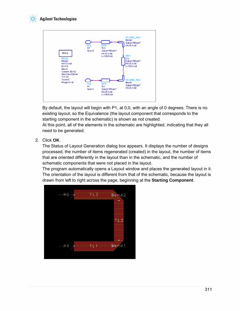
311
By default, the layout will begin with P1, at 0,0, with an angle of 0 degrees. There is no existing layout, so the Equivalence (the layout component that corresponds to the starting component in the schematic) is shown as not created. At this point, all of the elements in the schematic are highlighted, indicating that they all need to be generated.
2. Click OK. The Status of Layout Generation dialog box appears. It displays the number of designs processed, the number of items regenerated (created) in the layout, the number of items that are oriented differently in the layout than in the schematic, and the number of schematic components that were not placed in the layout. The program automatically opens a Layout window and places the generated layout in it. The orientation of the layout is different from that of the schematic, because the layout is drawn from left to right across the page, beginning at the Starting Component.

Electromagnetic
312
6.1.2 Creating a Layout Directly
Launch Advanced Design System and create a workspace. To display a Layout window, choose Window > New Layout from the ADS main window, or choose Window > Layout from an open Schematic window. The following tasks are performed the same way in a Layout window as they are in a Schematic window:
• Selecting components
• Placing and deselecting components
• Changing views
• Hiding component parameters
• Coping and rotating components
• Using named connections
Connecting Components with a Trace
As in a Schematic window, you can connect components without having them actually touch. In a Layout window, this is done by placing a trace between the component (in the same way a wire is used in the Schematic window). Either choose Component > Trace, or click the Trace button in the toolbar.
Unlike wires in a Schematic window, a trace in a Layout window may be inserted alone (click twice to end insertion).
6.1.3 Shapes
In Layout you can insert shapes, using either Insert commands or toolbar icons: With each shape, you can either click and drag to place it, or define points by coordinate entry (choose the shape, then choose Insert > Coordinate Entry ).
• path : starting point, segment end (click), and end point (double-click)
• polygon : starting point, vertex (click), and end point (double-click) that closes the shape
• polyline : starting point, segment end (click), and end point (double-click)
• rectangle : two diagonal corners
• circle : center and circumference point
• arc : (Insert command only) center and circumference point

313
Note The final segment of polygons and polylines can be entered by pressing the space-bar rather than double-clicking the mouse.
6.1.4 Layers
In a Layout window, items are placed on a layer. The name of the current insertion layer is displayed in the toolbar and in the status bar.
Changing the Insertion Layer
There are many ways to change the insertion layer:
• In the toolbar, retype the name of the layer and press Enter.
• In the toolbar, click the arrow next to the layer name. Choose a name from the list of currently defined layers.
• Choose the command Insert > Entry Layer and select a layer from the list.
• Choose the command Options > Layers and select a layer from the list of defined layers in the Layer Editor dialog box.
• Choose the command Insert > Change Entry Layer To , and click an object whose layer you wish to make the current insertion layer.
• Use the Layers window, that is opened when a Layout window is opened and select a name in the list of currently defined layers. Experiment with placing shapes on different layers. Remember to click OK to accept a change in a dialog box.
Copy to a Different Layer
Experiment with copying shapes from one layer to another; use the command Edit > Advanced Copy/Paste > Copy to Layer. Note that the copied shape is placed at exactly the same coordinates as the original. Move one to see them both.
Default Layer Settings
Choose the command Options > Layers to display the Layer Editor. This is where you can edit the parameters of any defined layer, add layers, or delete existing layers. Clicking Apply updates layer definitions but does not dismiss the dialog box.
Experiment with layer parameters. Note that you can toggle the visibility of all items on a layer. Protected means you can not select items on that layer.

Electromagnetic
314
Adjust Grid Visibility and Color 1. In the Display area, choose Major, Minor, or both.
2. Choose the Type of display (Dots or Lines). You may have to zoom in to see the grid display.
3. Click the colored rectangle next to the word Color, and choose the desired color for the grid. Click OK to dismiss the color palette.
4. Click Apply. Experiment with different settings
Note The drawing area color is the Background color under the Display tab.
Adjust Snap and Grid Spacing The ability to display a major grid as an increment of the minor grid enables you to gauge distances and align objects better in a layout.
1. In the Spacing area, change the Minor Grid display factors for both X and Y. The larger the number, the wider the grid spacing.
2. Click Apply. Experiment with different settings. If a display factor makes the grid too dense to display, it is invisible unless you zoom in.
3. Now experiment with the Major Grid.
Adjust Pin/Vertex Snap Distance Pin/vertex snap distance represents how close the cursor must be to a pin of a component or a vertex of a shape before the cursor will snap to it.
A large value makes it easier to place an object on a snap point when you are unsure of the exact location of the snap point. A small value makes it easier to select a given snap point that has several other snap points very near it.
Place several components and several shapes in the drawing area and experiment with different settings of Pin/Vertex Snap.
Screen pix specifies sizes in terms of pixels on the screen. For example, if you choose 15, the diameter of the snap region is 15 pixels.
User Units specifies sizes in terms of the current units of the window. For example, if you are using inches and choose 0.1 user units, the diameter of the snap region is 0.1 inch.

315
Experiment with Snap Modes Snap modes control where the program places objects on the page when you insert or move them; you can change snap modes when inserting or moving a component, or drawing a shape. When snap is enabled, items are pulled to the snap grid.
Experiment with different snap modes turned on or off to see how they affect the placement of items in a Layout window.
Snap Mode Priority You can restrict or enhance the manner in which the cursor snaps by choosing any combination of snap modes. This table lists the snap modes, and their priorities.
Pin 1 Vertex 2 Midpoint Intersect Arc/Circle Center Edge 3 Grid 4
Angle Snapping automatically occurs when only Pin snapping is enabled and you place a part so that the pin at the cursor connects to an existing part. The placed part rotates so that it properly aligns with the connected part.
For example, if you have a microstrip curve at 30° and place a microstrip line so that it connects to it, the microstrip line will snap to 30° so that it properly abuts the curve.
Enable Snap toggles snap mode on and off. You can also toggle snap mode from the Options menu itself, and there are snap mode buttons on the toolbar.
Except for pin snap, the pointer defines the selected point on the inserted object.
When you set all snap modes OFF, you can insert objects exactly where you release them on the page. This is sometimes called raw snap mode. Like other snap modes, the raw snap mode also applies when you move or stretch objects.
Pin When a pin on an object you insert, move, or stretch is within the snap distance of a pin on an existing object, the program inserts the object with its pin connected to the pin of the existing object. Pin snapping takes priority over all other snapping modes.

Electromagnetic
316
Vertex When the selected location on an object you insert, move, or stretch is within the snap distance of a vertex on an existing object, the program inserts that object with its selected location on the vertex of the existing object.
In vertex snap mode, a vertex is a control point or boundary corner on a primitive, or an intersection of construction lines.
Midpoint When the selected location on an object you insert, move, or stretch is within the snap distance of the midpoint of an existing object, the program inserts that object with its selected location on the midpoint of the existing object.
Intersect When the selected location on an object you insert, move, or stretch is within the snap distance of the intersection of the edges of two existing objects, the program inserts that object with its selected location on the intersection of the existing objects.
Arc/Circle Center When the selected location on an object you insert, move, or stretch is within the snap distance of the center of an existing arc or circle, the program inserts that object with its selected location on the midpoint of the existing arc or circle.
Edge When the selected location on an object you insert, move, or stretch is within the snap distance of the edge of an existing object, the program inserts that object with its selected location on the edge of the existing object. Once a point snaps to an edge, it is captured by that edge, and will slide along the edge unless you move the pointer out of the snap distance.
Because edge/centerline snapping has priority 3, if the cursor comes within snap distance of anything with priority 1 or 2 while sliding along an edge, it will snap the selected location to the priority 1 or 2 item.
Grid When the selected location on an object you insert, move, or stretch is within the snap distance of a grid point, the program inserts that object with its selected location on the grid point.
All other snap modes have priority over grid snap mode.
Hint Whenever possible, keep grid snapping on. Once an object is off the grid, it is difficult to get it back on. Use 45 or 90° angles to ensure that objects are aligned evenly, and to reduce the probability of small layout gaps due to round-off errors.

317
6.1.5 Drawing Tips
This section provides suggestions and examples when drawing layouts to be simulated using Momentum or FEM. These examples take into consideration things that are necessary during the drawing phase to ensure that requirements for an EM simulation are met.
Using Grid Snap Modes
Working in Layout enables you to control all geometry precisely. The variety of available snap modes can help you draw and position shapes. As an example, if you are connecting shapes, you should have the vertex snapping mode turned on. You will also want to review snap mode settings prior to adding ports to a layout.
Snap grid spacing also helps control the positioning shapes. In general, snap grid spacing should be about 1/2 of the minor grid point value. For example, if the minor grid points are 1.0, then the snap grid spacing should be 0.5. This makes it easy to know how your geometry will snap into place.
For more information on snap modes and snap grid spacing, refer to Layout.
Choosing Layout Layers
The standard set of layout layers begins with the layer named default. Do not use this layer for drawing your circuit. The first valid layer for an EM simulation is cond. For more information on layout layers, refer to Schematic Capture and Layout.
Keeping Shapes Simple
In general, when drawing shapes, you should use a minimal number of vertices per shape, since this will make the mesh easier to compute. When drawing curved objects, consider using a relatively large value for Arc/Circle Radius (under Options > Preferences > Entry/Edit ). This will minimize the number of vertices, and facets used to represent the shape.
Merging Shapes
Merging shapes is often useful for eliminating small geometry overlaps and can also, in some cases, result in simpler mesh patterns. For example, if you draw a layout using multiple polygons and you suspect there is some overlap, merging the polygons will prevent the system from returning an overlap error. To merge the shapes, select each shape that you want to merge, then choose Edit > Merge.
Viewing Port and Object Properties
Any item selected in a layout, including ports, shapes, or other components, has associated properties. One way to view the properties is to select the object of interest, then choose Edit > Properties. This method also enables you to change object properties. If you want to change properties that have been attributed to an object for an EM simulation, you should change these properties only through the EM Menu selections.
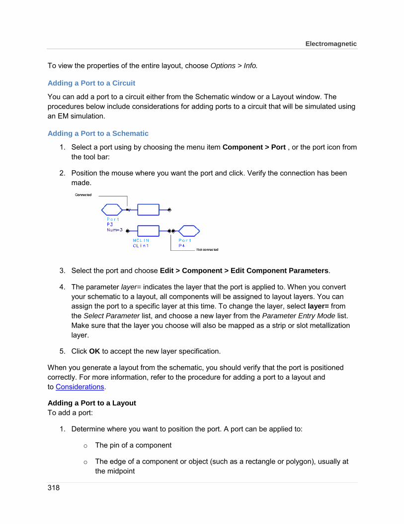
Electromagnetic
318
To view the properties of the entire layout, choose Options > Info.
Adding a Port to a Circuit
You can add a port to a circuit either from the Schematic window or a Layout window. The procedures below include considerations for adding ports to a circuit that will be simulated using an EM simulation.
Adding a Port to a Schematic
1. Select a port using by choosing the menu item Component > Port , or the port icon from the tool bar:
2. Position the mouse where you want the port and click. Verify the connection has been made.
3. Select the port and choose Edit > Component > Edit Component Parameters.
4. The parameter layer= indicates the layer that the port is applied to. When you convert your schematic to a layout, all components will be assigned to layout layers. You can assign the port to a specific layer at this time. To change the layer, select layer= from the Select Parameter list, and choose a new layer from the Parameter Entry Mode list. Make sure that the layer you choose will also be mapped as a strip or slot metallization layer.
5. Click OK to accept the new layer specification.
When you generate a layout from the schematic, you should verify that the port is positioned correctly. For more information, refer to the procedure for adding a port to a layout and to Considerations.
Adding a Port to a Layout To add a port:
1. Determine where you want to position the port. A port can be applied to:
o The pin of a component
o The edge of a component or object (such as a rectangle or polygon), usually at the midpoint

319
o The surface of an object
Note Do not place a port on the corner of an object. When you add a port to an edge, make sure the appropriate snap modes are enabled. It is a good practice to enable the modes Midpoint Snap and Edge/Centerline Snap (under the Options menu) to ensure accurate simulation results.
2. If you want to add a port to the surface of a polygon, you may need to disable the following or other snap modes (under the Options menu):
o Pin snap
o Edge/Centerline snap
o Midpoint snap
3. Identify the name of the layer on which the component or shape is entered. If you don't know the name of the layout layer, choose Options > Layers. Select each layer, noting the color in the dialog box. When the color matches that of the one in the Layout window, note the name of the layout layer. Dismiss the dialog box.
4. Select a port using by choosing the menu item Component > Port , or the port icon from the tool bar:
5. The Port parameters dialog box is displayed. The parameter layer indicates the layer that the port will be applied to. The parameter defaults to the currently active drawing layer.
6. This should be the same as the layer you noted in step 3. To change the layer, select layer= from the Select Parameter list, and choose a new layer from the Parameter Entry Mode listbox. Make sure that the layer you choose is also a strip or slot metallization layer. Do not apply ports to shapes that are on layers that are mapped to via metallization layers.
Note If you cannot find the layer name, choose Options > Layers , then select the layer name of interest from the Layers list. Note the layer number in the Number field. In the Port dialog box, select the layer= parameter and, under Parameter Entry Mode,

Electromagnetic
320
select Integer Value. Enter the layer number, then click Apply.
7. Click Apply to accept the new layer specification.
8. Position the mouse where you want to place the port and click. The port is added to the circuit.
Note If you are applying a port to an edge, the port must be positioned so that the arrow is outside of the object, pointing inwards, and at a straight angle. Generally, this happens automatically when you add a port to an edge. You may need to zoom in to verify this.
9. The Instance Name in the Port dialog box is incremented if you want to add another port. Verify the layer= parameter, then use the mouse to add the next port.
10. When you are finished adding ports, click OK to dismiss the dialog box.
Considerations Keep the following points in mind when adding ports to circuits to be simulated using Momentum or FEM:
• The components or shapes that ports are connected to must be on layout layers that are mapped to metallization layers that are defined as strips or slots. Ports cannot be directly connected to vias.
• Make sure that ports on edges are positioned so that the arrow is outside of the object, pointing inwards, and at a straight angle.
• Make sure that the port and the object you are connecting it to are on the same layout layer. For convenience, you can set the entry layer to this layer; the Entry Layer listbox is on the Layout tool bar.
• A port must be applied to an object. If a port is applied in open space so that is not connected to an object, Momentum will automatically snap the port to the edge of the closest object. This will not be apparent from the layout, however, because the position of the port will not change.

321
• If the Layout resolution is changed after adding ports that are snapped to edges, you must delete the ports and add them again. The resolution change makes it unclear to which edges the ports are snapped, causing errors in mesh calculations.
Note Do not use the ground port component in circuits that will be simulated using Momentum ( Component > Ground or the toolbar button). Either add ground planes to the substrate or use the ground reference ports that are described later in this section.
6.2 Using EM Tools Using the Cookie cutter and Copy to design tools, you can create a new cell view and copy selected designs. This section provides information about how to create new designs using your existing design.
6.2.1 Cookie Cutter
You can create a new cell view containing a cookie cut area around selected objects. The Cookie Cutter feature enables you to crop only the required area from an original design. You can create the following types of boundary:
• Bounding Box: Represents the smallest rectangle that contains the selected shapes.
• Convex Hull: Represents the smallest convex set that contains the selected shapes.
To use a cookie cutter, you need to define a boundary layer, which is drawn for previewing and cutting operation. Note that cookie cutter is not applied to the shapes on a boundary layer. Therefore, you need to select a layer that does not include real patterns where you want to use this feature.
Based on the objects that have selected in the original design, a new design is created. You can specify the name for your new design in the Output field.
If you have selected the Cut instances if it is on the boundary option, the instances with its box intersects with the boundary will be cut and the instance itself will be deleted. Otherwise, such instances are not displayed in the output design.
Cookie cutter works with objects that are selected by any type of selection mechanism provided by ADS, such as manual selection and Physical Connectivity Engine. Therefore, you can use the Cookie cutter, even if the Physical Connectivity Engine is switched off.
To create a cookie cut cell view:

Electromagnetic
322
1. Select EM > Tools > Cookie Cutter.
2. Select the required objects in the layout window. You can select objects either manually or use the Navigator feature.
3. Select the boundary type and specify an oversize distance.
4. Select the boundary Layer.
5. Click Preview to check boundary shape.
6. Click ... to select output design name.
7. Select option.
8. Select Cut instances if it is on the boundary.

323
9. Click OK to create a cut boundary. Another layout window opens, which contains the area that was cut by the boundary.
6.2.2 Copying the Selected Design to a New Cell View
To copy selected objects:
1. Select EM > Tools > Copy To Design.
2. Select the required objects in the layout window by manual selection, using the Navigator, or any other method
3. Click to select a target layout.
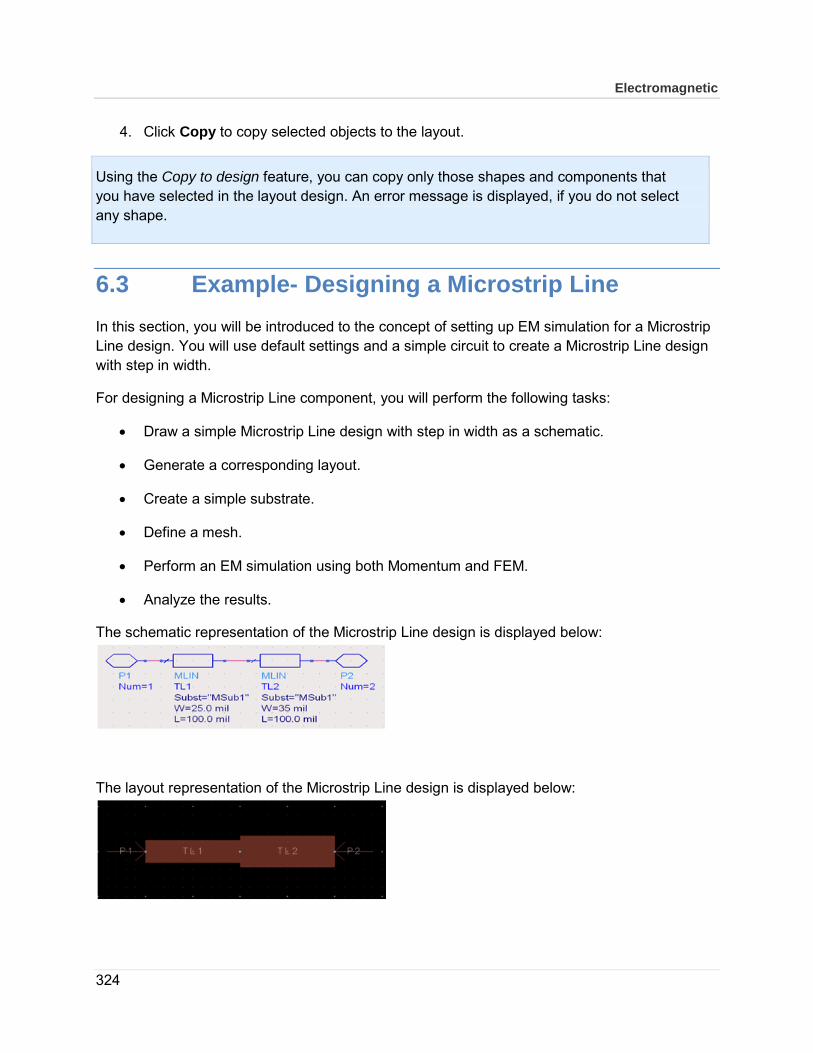
Electromagnetic
324
4. Click Copy to copy selected objects to the layout.
Using the Copy to design feature, you can copy only those shapes and components that you have selected in the layout design. An error message is displayed, if you do not select any shape.
6.3 Example- Designing a Microstrip Line In this section, you will be introduced to the concept of setting up EM simulation for a Microstrip Line design. You will use default settings and a simple circuit to create a Microstrip Line design with step in width.
For designing a Microstrip Line component, you will perform the following tasks:
• Draw a simple Microstrip Line design with step in width as a schematic.
• Generate a corresponding layout.
• Create a simple substrate.
• Define a mesh.
• Perform an EM simulation using both Momentum and FEM.
• Analyze the results.
The schematic representation of the Microstrip Line design is displayed below:
The layout representation of the Microstrip Line design is displayed below:

325
6.3.1 Drawing the Circuit
To start the process of designing a Microstrip Line component, you need to draw the circuit by:
• Creating a new workspace.
• Adding Microstrip components to the schematic.
• Converting the schematic to a layout.
6.3.2 Creating a New Workspace
To create a new workspace:
1. From the ADS Main window, choose File > New > Workspace to display New Workspace Wizard.
2. Click Next.
3. In the Workspace Name field, type step1.
4. Enter a path in Create In. Click Browse to select the location.
5. Click Next.
6. Under Add Libraries, select the libraries to be included in the Workspace, as shown in the following figure:
7. Click Next.
8. Under Library Name, enter a unique library name.
9. Click Next.

Electromagnetic
326
10. Under Technology, choose ADS Standard: length unit - mil.
11. Click Finish.
For more information about a workspace, refer Workspace.
6.3.3 Adding Microstrip Line components to the Schematic
To create a new schematic:
1. Choose File > New > Schematic.
2. Create a new schematic step_1 in library step_1_lib.
For more information about a schematic, refer to Creating a New Schematic.
After creating a schematic, select a component and place it in the Schematic window.
6.3.4 Placing Components in a Schematic
To select and place components in a Schematic window:
1. Click the Palette drop-down list.
2. Select TLines-Microstrip from the list.

327
3. Click MLin in the Microstrip Transmission Lines palette.
4. Move the crosshairs to the Schematic window and click once to place the component. A schematic representation of the component is placed in the Schematic window.
5. Move the cursor to place the crosshairs directly on the right pin of the first component, and then click once to place the second component.
Canceling Commands
If you continue to click without ending the current command, you will add another component
with each click. To cancel a command, click the arrow button ( ). You can also end a command by pressing the Escape key.
6.3.5 Editing Component Parameters
This section describes how to change the width of one of the strips to create a Microstrip Line step in width transmission line.
To edit components:

Electromagnetic
328
1. Click twice on the second component that you placed. The Libra Microstrip Line dialog box opens.
2. In the Select Parameter field, select the W to specify the width. When the field to the right shows the value of the width, change the value in this field to 35 mil.
3. Click Apply.
4. Click OK.
Note If a parameter for a component is displayed in the Schematic window, you can also edit that parameter by clicking the value and entering a new value.
5. Verify that the width of component on the left is set to 25 mil.
6.3.6 Adding Pins to the Circuit
To complete the circuit, you must add pins, one at the beginning of the Microstrip Line component step in width and one at the end. This section describes how to add pins to the circuit.
To add pins:
1. Click Pin ( ) in the menu bar.

329
2. Move the cursor over the Schematic window and note the orientation of the ghost icon of the pin.
3. Click Rotate to rotate the port to the necessary orientation.
4. Move the cursor over the open pin on the left side of the left component, then click once.
5. To insert a second port, change the orientation appropriately, move the cursor over the open pin on the right side of the right component, then click once.
6. Click to cancel the current command. Your schematic displays a Microstrip Line step in width. The width of the first part of the line is 25 mil, and it increases to a width of 35 mil. The overall length is 200 mil, as shown in the following figure:
Note Diamond-shaped pins indicate that pins are not connected. You need to select and move components to form complete connections.
6.3.7 Saving a Design
To save your design, choose File > Save.
6.3.8 Generating a Layout
Since EM simulations require a circuit in the layout format, it gives you the option of drawing your circuits either as schematics or as layouts.
Note If you choose to draw in a Schematic window, footprints of the components you use must also be available in Layout. Components that are available in Layout include transmission lines and lumped components with artwork.
To covert the Microstrip Line design with step in width schematic:

Electromagnetic
330
1. In the Schematic window, choose Layout > Generate/Update Layout. The Generate/Update Layout dialog box appears. It is not necessary to edit fields.
2. Click OK. The Layout Generation message appears indicating that the conversion is complete.
3. Click OK.
4. A Layout window appears, which displays a layout representation of the schematic. This window may be hidden by the Schematic window, so you may need to move some windows to locate the Layout window.
5. From the Layout window, choose File > Save. You now have a layout and a schematic as part of your library step_1.
6.3.9 Creating a Simple Substrate
A substrate is required as part of your planar circuit. The substrate describes the media where the circuit exists. An example of a substrate is the substrate of a multilayer circuit board, which consists of:
• Layers of metal traces
• Layers of insulating material between the traces
• Ground planes
• Vias connecting traces on different layers
• Air surrounding the circuit board
In ADS 2011, substrates are part of the Technology dialog box used for a library. For the Microstrip Line design having step in width example, a substrate having the following layers is used:
• Ground plane
• Dielectric(insulation), such as Alumina
• Metal layer for the Microstrip Line component
• Air layer above the Microstrip component

331
6.3.10 Defining the EM Setup
In the EM Setup window, you can specify settings for running a successful EM simulation. If you do not provide correct information, an invalid symbol ( ) appears against the options in the left pane of the EM Setup window.
To specify the EM simulation settings:
1. Choose EM > Simulation Setup to open the EM Setup window.
2. Select Substrate in the left pane of the EM Setup window.
3. Select Frequency Plan and add the frequency range for simulation. By default, an adaptive frequency plan from 0 Ghz to 10 Ghz is added. The EM setup becomes valid on adding the frequency plan. For more information, refer to Defining a Frequency Plan.
Note At this stage, if you want to start the simulation, click the Simulate button at the bottom of EM Setup window.
4. Select Layout to gather information about the Layout for which this EM setup is prepared. For more information, refer to Viewing Layout Information.
5. Select Substrate to display the substrate used for the simulation. For more information, refer to Defining Substrates in EM Simulations.

Electromagnetic
332
6. Select Ports to gather information about the ports being generated from the pins defined in the layout. EM simulations need ports to inject energy into system. For more information, refer to Defining Ports in EM Simulations.
7. Select Output plan to specify a name for the EM dataset.
8. Select Options to specify mesh, preprocessor, and solver options. For more information, refer to Defining Simulation Options.
9. Select Resources to specify computer resources options. For more information, refer to Specifying Simulation Resources.
10. Select Model/Symbol to generate an EM model and symbol. For more information, refer to Generating an EM Model and Symbol.
11. Select Note to add any specific note about the simulation.
12. Save the EM settings by selecting File > Save.
13. Click Simulate in the EM Setup window to start the EEsof Job manager and EEsof Job log window for the currently running momentum simulation.
14. After the simulation is complete, the Data Display window opens automatically:

333
6.3.11 Viewing Results
Load S11 plot on the Data Display window, as shown in the following figure:
6.3.12 Switching Simulation Engines
For changing the mode of simulation to FEM, open the EM Setup window and select FEM. Once the mode is changed to FEM, the EM setup remains valid for the FEM simulator.
Note Selecting the FEM simulator changes the dataset name in Output plan to step1_fem.
Clicking Simulate in the EM Setup window launches the EEsof Log window for the FEM simulation. After completion of the FEM simulation, a data display window is displayed:

Electromagnetic
334
S11 plot for FEM is shown below:
6.3.13 Comparing Momentum and FEM Results
Load the plots from both Momentum and FEM and compare the results. Comparison plots are shown below:

335
Chapter 7 – Running EM Simulations The simulation process generates a mesh for the circuit and solves E-fields in the circuit. Using these electric field calculations, S-parameters are calculated for the circuit. The mesh electric field is then refined and new electric fields and S-parameters are computed. Before running a simulation, the following criteria must be met:
• A substrate definition must be specified for the circuit.
• The circuit must include at least one port.
• The mesh is automatically calculated when you simulate.
• A simulation frequency plan must be specified.
If any one of the above criteria is not met, an error is generated if you try to run a simulation.
7.1 Starting an EM Simulation To start a simulation:
1. Choose EM > Simulation Setup.
2. In the EM Setup window:
o Verify that at least one frequency plan appears in the Frequency Plans list.
o Check that the Process Mode, Solution Files, and Data Display options are set to your specifications.
o Check whether the simulation mode is set to local machine.

Electromagnetic
336
3. Click Simulate in the EM Setup window or press F7. A data display opens automatically to display the results.
7.2 Viewing Simulation Status When you start a simulation, new job entry is created in the Job manager. For more information, refer to the Using the Job Manager document. If the simulation has to wait in a Job Manager queue, the new entry in main Job Manager window is displayed. You can double-click this entry to open a detailed log window. If the simulation does not need to wait, the log window is immediately displayed, which displays the simulation status and simulation messages. Messages usually refer to any errors found, the percent of completion (refer to Understanding the "% Covered" Status Message) and simulation completion. If you close the log window and want to reopen it, double-click the job entry in the main Job Manager window. To open this window from a layout window, choose Window > Simulation Status.
To indicate progress, a progress bar appears at the bottom of the log window, if the number of unknowns in the simulation is greater than 500; otherwise, only the frequencies are displayed. If a simulation fails due to setup related issues, partial data is saved and a message appears in the log window.
7.2.1 Understanding the "% Covered" Status Message
This message is generated when running Adaptive sweep types. It indicates the percentage of the total simulation frequency range that has been accurately modeled by rational functions.

337
When an Adaptive sweep starts, the AFS process attempts to represent all S-parameters with a number of rational functions. New sample points are selected adaptively (by minimizing global error criteria). If the frequency range is too large, the frequency range will be split into sections. If the fitting model is accurate and stable within a subrange, the "% covered" message will be updated. Thus, the message indicates the percentage of the total simulation frequency range that has been accurately modeled by rational functions.
7.3 Stopping an EM Simulation To stop an EM simulation, choose EM > Stop and Release Simulator. Alternatively, the simulation can be stopped using Job > Stop/Cancel Job in the Using the Job Manager.
7.4 Viewing the Simulation Summary As a simulation progresses, you can view solution statistics. Some of the information returned includes time to solve, the resources required, mesh information, and any messages that were displayed in the status window.
Choose EM > Show Most Recent and select one of the following option to view the required data:
• Momentum Mesh
• S-Param Simulation Summary
• Mesh Generation Summary
• Geometry Preproc Report
• Substrate Generation Summary
The following example shows a (partial) summary displayed when using the Momentum Microwave simulation mode.
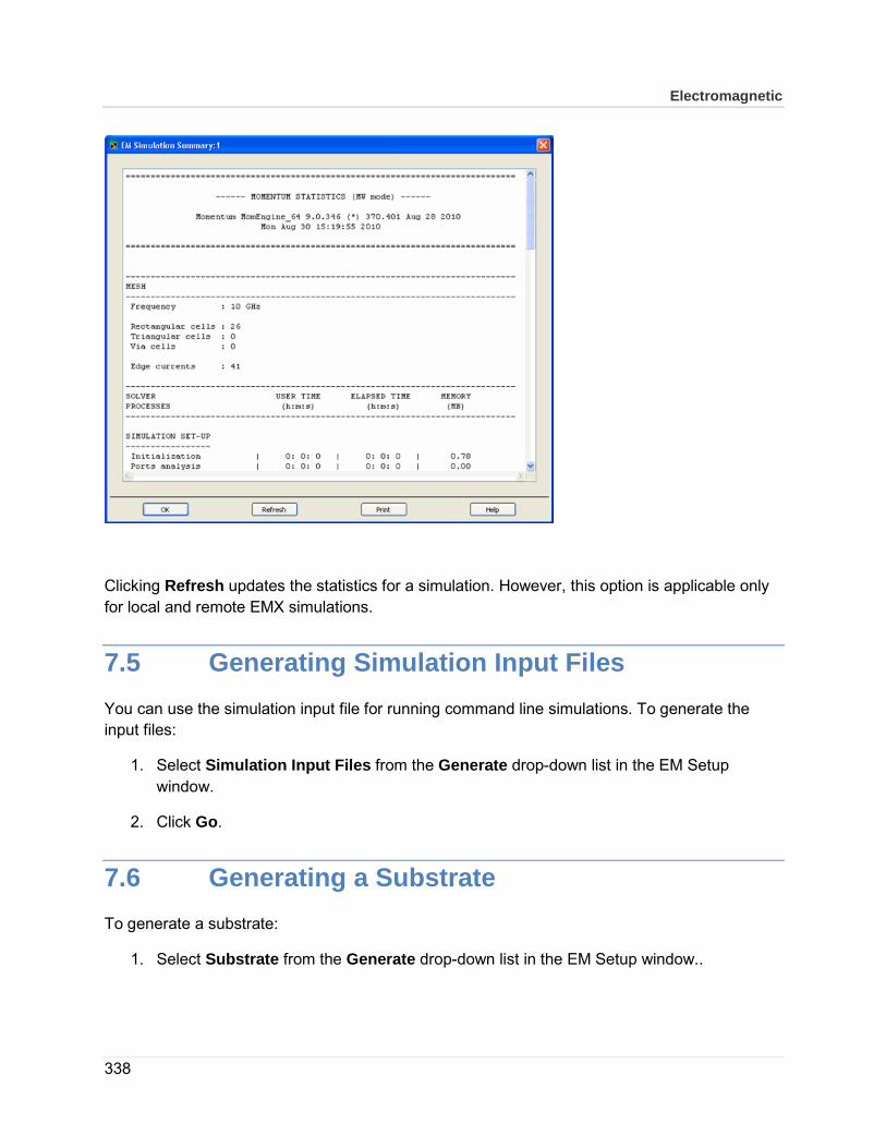
Electromagnetic
338
Clicking Refresh updates the statistics for a simulation. However, this option is applicable only for local and remote EMX simulations.
7.5 Generating Simulation Input Files You can use the simulation input file for running command line simulations. To generate the input files:
1. Select Simulation Input Files from the Generate drop-down list in the EM Setup window.
2. Click Go.
7.6 Generating a Substrate To generate a substrate:
1. Select Substrate from the Generate drop-down list in the EM Setup window..
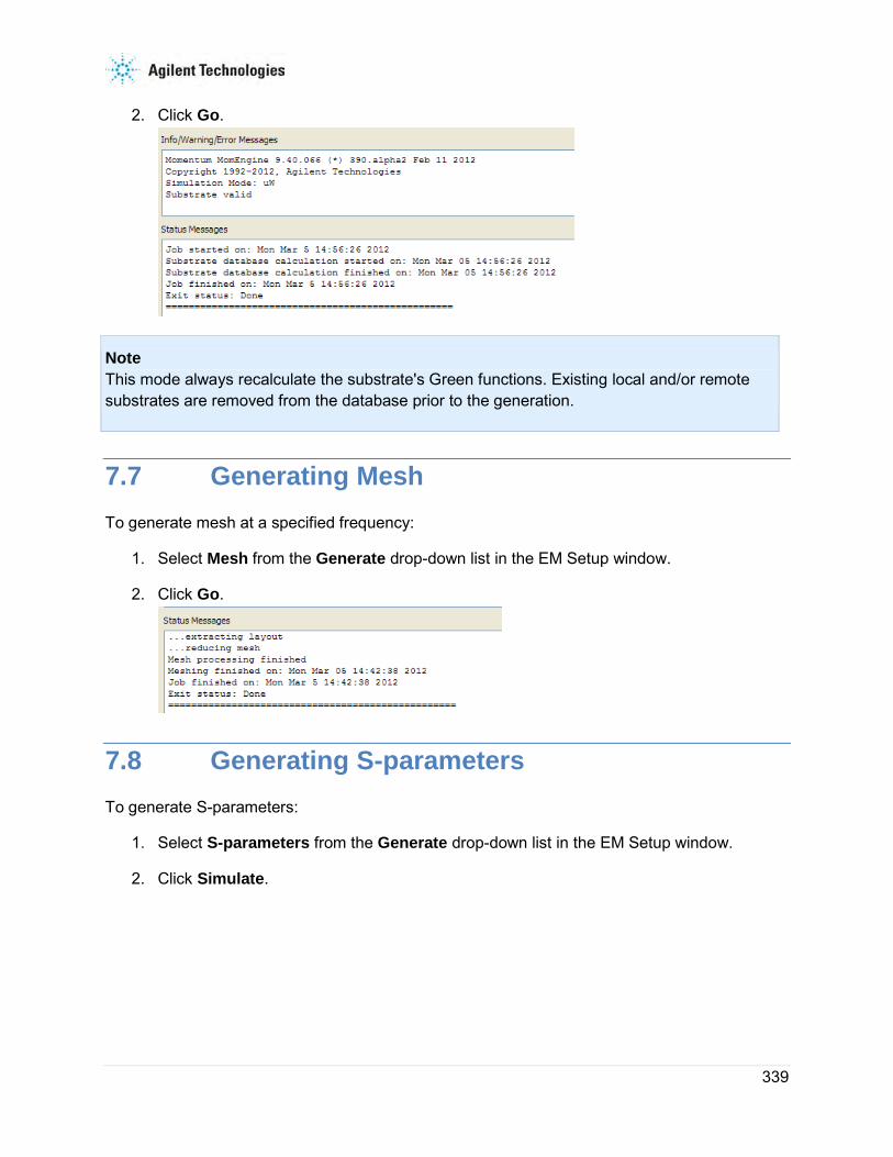
339
2. Click Go.
Note This mode always recalculate the substrate's Green functions. Existing local and/or remote substrates are removed from the database prior to the generation.
7.7 Generating Mesh To generate mesh at a specified frequency:
1. Select Mesh from the Generate drop-down list in the EM Setup window.
2. Click Go.
7.8 Generating S-parameters To generate S-parameters:
1. Select S-parameters from the Generate drop-down list in the EM Setup window.
2. Click Simulate.

Electromagnetic
340
Chapter 8 – Viewing 3D Simulations
Using the EM visualization feature, you can view and analyze the following types of simulation data:
• S-parameters
• Currents
• far-fields
• Antenna parameters
• Transmission line data
8.1 Starting an EM Visualization Before using the visualization feature, you should complete the simulation process. After simulating your design, choose EM > Post-Processing > Visualization to open the
Visualization window. You can also open this window by clicking Visualization in the EM toolbar. The following figure displays a Visualization window:

341
The Visualization window controls the display of the individual mask layers, substrates, and port boundaries. In the Visualization window, the left pane contains the basic controls for the view in the docking widget.
This section provides information about the following topics:
• Visualizing 3D View before EM Simulations
• Visualizing Momentum Simulations
• Visualizing FEM Simulations
• Computing Radiation Patterns
• Viewing Simulation Summary
8.2 Visualizing 3D View before EM Simulations Before simulating a design, you can validate your three dimensional design in the 3D Preview window. The representation seen in the 3D viewer consists of the same definition that will be used in the EM simulator. If a view is incorrect in the 3D viewer, it is essential to redesign before attempting a simulation. The following figure displays a 3D Preview window:
The key benefits of this visual confirmation are:
• Correct Substrate Set Up: The substrate information within ADS is defined by using the Substrate menu options, which help you to define the height of each substrate and

Electromagnetic
342
assign the corresponding layers. The Previewer window enables you to validate that correct height and mappings are specified for your design.
• Correct Bondwire and Dielectric Brick Placement: Bondwires, which are described in the schematic window of ADS, are mapped to the ADS layout and incorporated into the overall FEM design for simulation. Dielectric bricks are defined as part of the substrate definition. Since these portions of the design are difficult to see in layout, you can use the Previewer window to validate the location and design of bondwires.
You can create the following types of 3D views:
• Layout View: Select View > 3D View > All to generate a 3D view of the layout without any EM pre-processing. This is the fastest way to generate a 3D view. You do not to create an EM Setup view for generating the 3D view from layout. The first substrate found in the library will be used.
If you select View > 3D View > Selection to generate a 3D view of the selected components, pins are not displayed in the Preview window.
• Momentum Simulator View: Click the 3D EM Preview icon from the EM toolbar, EM menu, or EM Setup window with Momentum specified as simulator type to generate a 3D view that displays the design in 3D as seen by Momentum, including any specified pre-processing operations.
• FEM Simulator View: Click the 3D EM Preview icon from the EM toolbar, EM menu, or EM Setup window with FEM specified as simulator type to generate a 3D view that displays the design in 3D as seen by FEM, including any specified pre-processing operations.
If pins are not properly aligned on the bounding box of a design, it causes an invalid simulation set up. The 3D View from the Momentum perspective does not cause failure, since it does not support Waveguide Ports. On the FEM side, the waveguide ports are validated and if they fail validation, no design is exported for preview. To avoid this problem, move the pins in your ADS design so that they are properly aligned on the bounding box.

343
8.2.1 Validating Your Geometry Visually
You can validate a geometry by opening the 3D Preview window in a layout. Before reviewing your design, you need to start the previewer regularly, as it does not synchronize with the current ADS layout.
Note It is recommended that you do not keep more than one instance of the previewer open at a time. It will not interfere with the data, however, it may be confusing and cause an unnecessary error.
The previewer window contains a dockable widget that controls the display of the individual mask layers, substrates, and port boundaries. Upon startup, a dockable widget is docked on the left-hand side of the previewer, as shown in the following figure:
8.2.2 Navigating in the 3D Environment
You can perform the following tasks in the 3D Preview window:
• Rotating the view: You can rotate a design around its current origin by holding down the main mouse button and moving it around the screen. Click Orbit ( ) on the toolbar or choose Window > Orbit to rotate a view.

Electromagnetic
344
• Modifying the zoom settings: You can increase or decrease the zoom settings on a
design by moving the mouse up or down on the image respectively. Click Zoom ( ) on the toolbar or select Window > Zoom to modify zoom settings.
• Moving the design: You can move the design around on the screen by holding down
the main mouse button and moving it around the screen. Click Pan ( ) on the toolbar or select Window > Pan to move a design.
• Opening the standard view: You can change the view of a design to the standard view
settings. Click Zoom to Extents ( ) on the toolbar or select Window > Zoom to Extents to open the standard view for your design.
• Modifying the zoom settings of a specific area: You can zoom to a specific area of
your design by placing a box around the desired view. Click Zoom to Window ( ) from the toolbar or select Window > Zoom to Window to change the zoom settings.
• Changing Views: You can open your design in various types of standard views by
clicking Front ( ), Back ( ), Top ( ), Bottom ( ), Left-side ( ),
Right-side ( ), and Isometric ( ). You can also access these views from the View menu.
• Querying the design: You can click an object edge or vertex to display the location and object name in the status bar, which is located in the lower right hand section of the window. In addition, the object is highlighted and the object is automatically selected in the Object and Material tabs in the Docking widget. Visually, a solid dot is placed if the selected location is on a vertex and a hollow dot is placed if the selected location is on
an edge. Click Query ( ) or select Tools > Query to run a query.
8.2.3 Exporting Field Data
You can export E or H fields data by using the Advanced Visualization window. In addition to exporting the field data per tetrahedra, you can export the data per uniform grid.
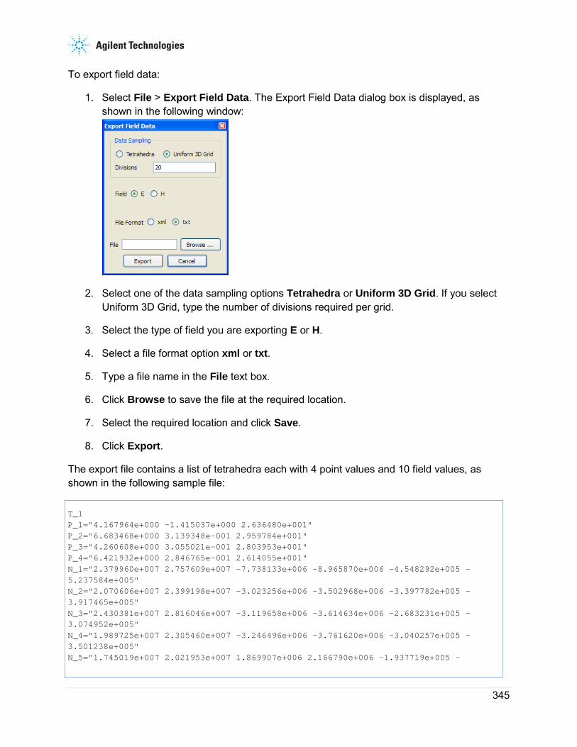
345
To export field data:
1. Select File > Export Field Data. The Export Field Data dialog box is displayed, as shown in the following window:
2. Select one of the data sampling options Tetrahedra or Uniform 3D Grid. If you select Uniform 3D Grid, type the number of divisions required per grid.
3. Select the type of field you are exporting E or H.
4. Select a file format option xml or txt.
5. Type a file name in the File text box.
6. Click Browse to save the file at the required location.
7. Select the required location and click Save.
8. Click Export.
The export file contains a list of tetrahedra each with 4 point values and 10 field values, as shown in the following sample file:
T_1 P_1="4.167964e+000 -1.415037e+000 2.636480e+001" P_2="6.683468e+000 3.139348e-001 2.959784e+001" P_3="4.260608e+000 3.055021e-001 2.803953e+001" P_4="6.421932e+000 2.846765e-001 2.614055e+001" N_1="2.379960e+007 2.757609e+007 -7.738133e+006 -8.965870e+006 -4.548292e+005 -5.237584e+005" N_2="2.070606e+007 2.399198e+007 -3.023256e+006 -3.502968e+006 -3.397782e+005 -3.917465e+005" N_3="2.430381e+007 2.816046e+007 -3.119658e+006 -3.614634e+006 -2.683231e+005 -3.074952e+005" N_4="1.989725e+007 2.305460e+007 -3.246496e+006 -3.761620e+006 -3.040257e+005 -3.501238e+005" N_5="1.745019e+007 2.021953e+007 1.869907e+006 2.166790e+006 -1.937719e+005 -

Electromagnetic
346
2.238154e+005" N_6="2.117090e+007 2.453070e+007 1.722775e+006 1.996282e+006 -2.439926e+005 -2.807636e+005" N_7="1.672967e+007 1.938458e+007 1.558138e+006 1.805409e+006 -1.685716e+005 -1.944367e+005" N_8="2.481198e+007 2.874945e+007 1.584858e+006 1.836456e+006 -1.704304e+005 -1.940710e+005" N_9="2.035784e+007 2.358837e+007 1.409211e+006 1.632806e+006 -2.056144e+005 -2.360936e+005" N_10="1.599067e+007 1.852821e+007 1.252236e+006 1.450838e+006 -1.420236e+005 -1.634942e+005"
In the export file, the point values (P_1 to P_4) represents the X, Y, Z coordinates of the four vertices of each tetrahedron. The ten field values (N_1 to N_10) represents the field strengths at each of the four vertices and the midpoints of the six edges of each tetrahedron. Each value contains the real and imaginary parts of the x, y and z field components.
8.2.4 Specifying Material and Object Settings
In the 3D Preview window, you can control the material and object settings by using the Properties window. Click to separate the Properties window from the 3D Preview window. To include the Properties dialog box, double-click the Properties title bar. The following figure
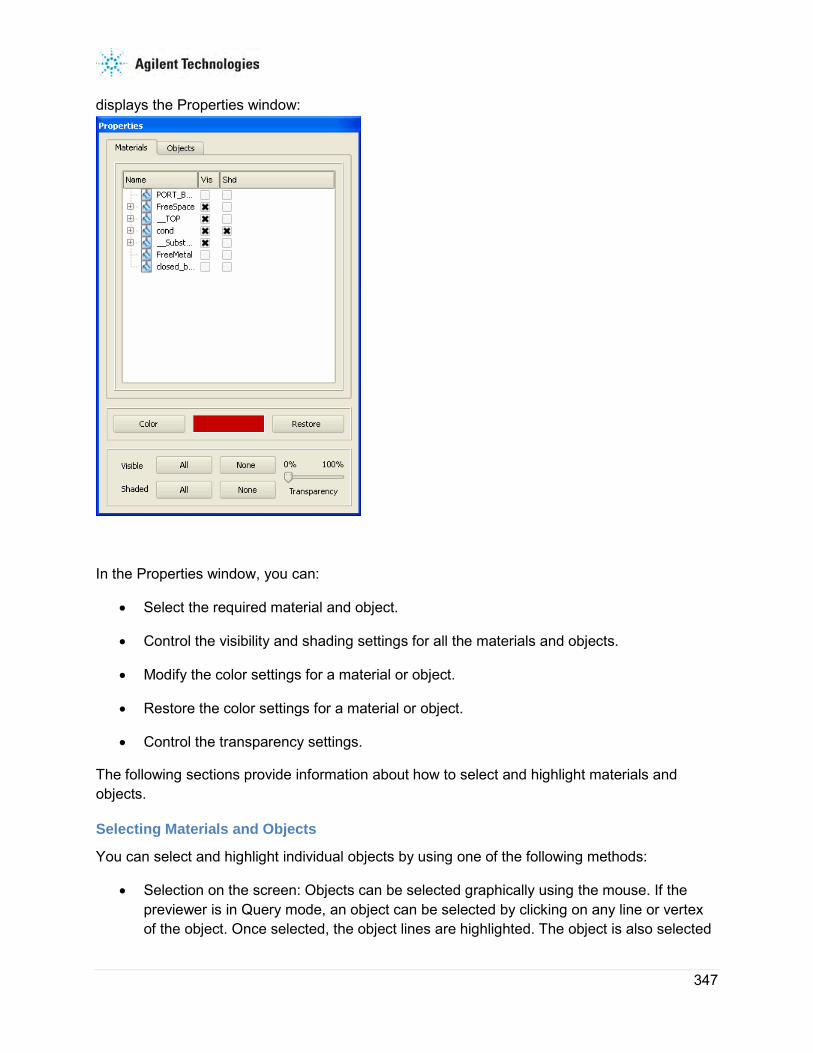
347
displays the Properties window:
In the Properties window, you can:
• Select the required material and object.
• Control the visibility and shading settings for all the materials and objects.
• Modify the color settings for a material or object.
• Restore the color settings for a material or object.
• Control the transparency settings.
The following sections provide information about how to select and highlight materials and objects.
Selecting Materials and Objects
You can select and highlight individual objects by using one of the following methods:
• Selection on the screen: Objects can be selected graphically using the mouse. If the previewer is in Query mode, an object can be selected by clicking on any line or vertex of the object. Once selected, the object lines are highlighted. The object is also selected
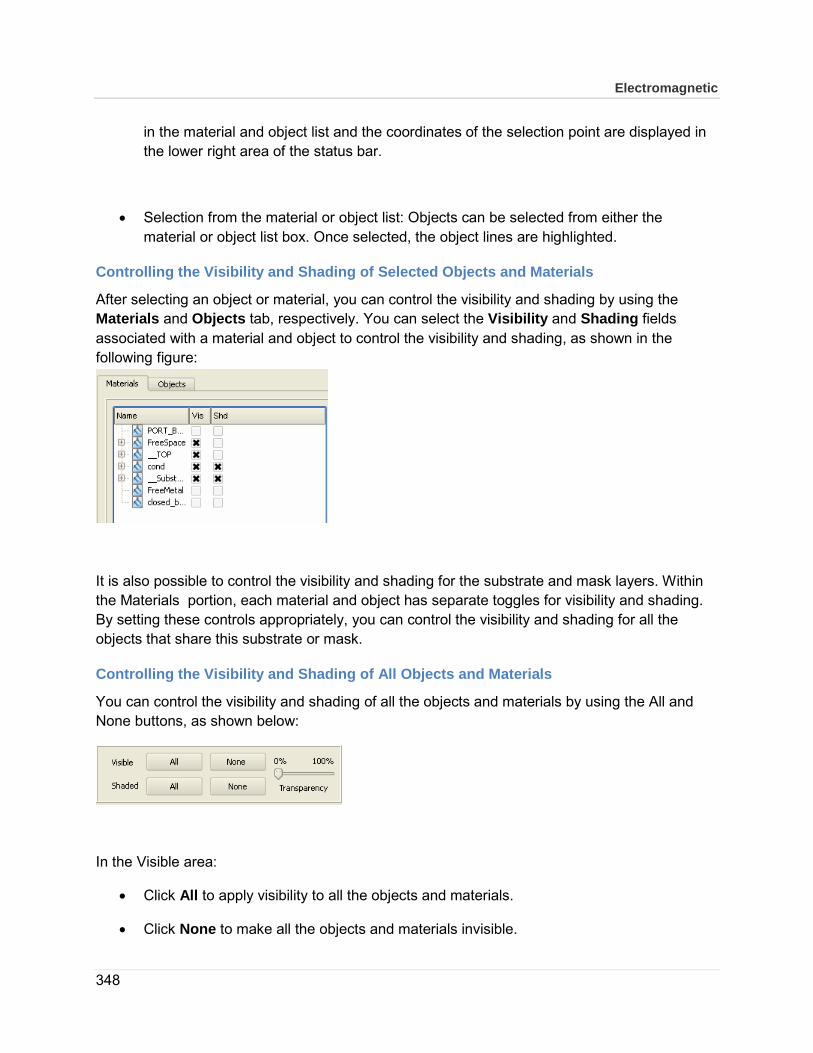
Electromagnetic
348
in the material and object list and the coordinates of the selection point are displayed in the lower right area of the status bar.
• Selection from the material or object list: Objects can be selected from either the material or object list box. Once selected, the object lines are highlighted.
Controlling the Visibility and Shading of Selected Objects and Materials
After selecting an object or material, you can control the visibility and shading by using the Materials and Objects tab, respectively. You can select the Visibility and Shading fields associated with a material and object to control the visibility and shading, as shown in the following figure:
It is also possible to control the visibility and shading for the substrate and mask layers. Within the Materials portion, each material and object has separate toggles for visibility and shading. By setting these controls appropriately, you can control the visibility and shading for all the objects that share this substrate or mask.
Controlling the Visibility and Shading of All Objects and Materials
You can control the visibility and shading of all the objects and materials by using the All and None buttons, as shown below:
In the Visible area:
• Click All to apply visibility to all the objects and materials.
• Click None to make all the objects and materials invisible.
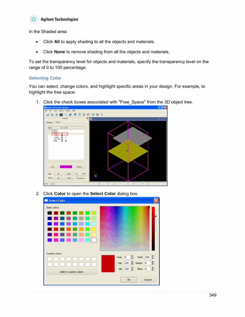
349
In the Shaded area:
• Click All to apply shading to all the objects and materials.
• Click None to remove shading from all the objects and materials.
To set the transparency level for objects and materials, specify the transparency level on the range of 0 to 100 percentage.
Selecting Color
You can select, change colors, and highlight specific areas in your design. For example, to highlight the free space:
1. Click the check boxes associated with "Free_Space" from the 3D object tree.
2. Click Color to open the Select Color dialog box.

Electromagnetic
350
3. Select a color and click OK.
4. You can revert the original color by clicking Restore.
8.2.5 Customizing the Simulation View
• Measuring distances: You can measure the distance between a reference point and the current query point. The query point is updated after every mouse selection using the query command. The reference point remains fixed until it is explicitly updated using the Move Current Point to Reference. Select Tools > Measure to open the Measure dialog box:
• Z-Scaling: You can change the geometry dimension of a model in the z-direction using a sliding scale between 1 and 10. If you move the dimension value of the slide bar up, the model is expanded in the z-direction. Select Tools > Z Scale to open the z-scale dialog box.
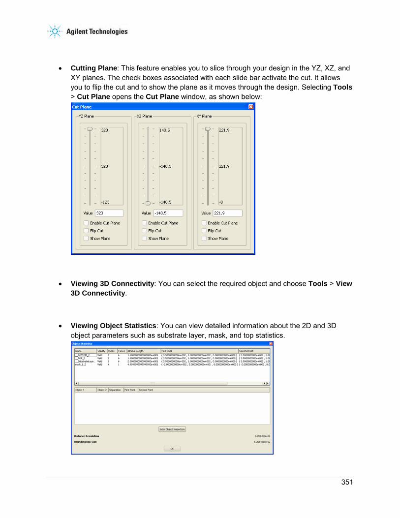
351
• Cutting Plane: This feature enables you to slice through your design in the YZ, XZ, and XY planes. The check boxes associated with each slide bar activate the cut. It allows you to flip the cut and to show the plane as it moves through the design. Selecting Tools > Cut Plane opens the Cut Plane window, as shown below:
• Viewing 3D Connectivity: You can select the required object and choose Tools > View 3D Connectivity.
• Viewing Object Statistics: You can view detailed information about the 2D and 3D object parameters such as substrate layer, mask, and top statistics.

Electromagnetic
352
8.2.6 Setting Up the Viewer on External X Window Displays
On Unix/Linux Systems, it is common practice to use a local machine as a display and do the actual processing on another machine. The display from the original machine is typically mapped back to the local display using the following command:
export DISPLAY=machine:0.0
In the 3D Previewer window, you need to set an additional environment variable, HOOPS_PICTURE. This environment variable is set to the same value as the display variable with the addition of X11/ prior to the machine name. Using the above example, the HOOPS_PICTURE variable is set to the following values:
export HOOPS_PICTURE=X11/machine:0.0
8.3 Visualizing FEM Simulations You can view and analyze the following type of data for FEM simulations:
• E Fields
• Far-fields
• Antenna parameters
• Transmission line data
8.3.1 Starting FEM Visualization
You must complete the simulation process to view data for your FEM design. If you have already simulated a design, start the Visualization feature directly to view the existing data. Select EM > Post-Processing > Visualization to open the Agilent FEM Visualization window.
You can also open this window by clicking Visualization ( ) in the EM toolbar.
To visualize FEM simulations:
1. Choose EM > Simulation Setup to open the EM Setup window.
2. Select FEM in the EM Setup window.

353
3. Specify the required settings in the EM Setup window for a layout, substrate, port, frequency plan, output plan, options, resources and model or symbol.
4. Click Simulate in the EM Setup window to simulate your design.
5. Select EM > Post-Processing > Visualization.
The Agilent FEM Visualization window appears similar to the EM Previewer window. The initial window layout is similar to that of an EM Previewer. The left side contains the basic controls for the view in the docking widget. However, the Agilent FEM Visualization window includes the following modifications:
• EM Port surfaces are no longer displayed.
• Object shading is removed.
• A shaded current plot for Port 1 at the lowest frequency is displayed.
• In addition to the Properties tab, Solution Setup and Plot Properties tabs are added for controlling the view.
The Properties tab provides the same functionality as the Previewer properties tab. However, in the Agilent FEM Visualization window, you can specify the type of mesh: Surface or Volume Mesh, as shown in the following figure:

Electromagnetic
354
Note For more information about the Properties tab, refer Visualizing 3D View before EM Simulations.
You can display the field quantities by using the Plot Properties and Solution Setup tabs. The Solution Setup tab controls the excitations for the visualization, while the Plot Properties tab controls the visual display of the excitation.
8.3.2 Controlling Visualization Excitations
The Solution Setup tab is used to select the current excitation for the plots. All the plots automatically reflect the current solution configuration once it is selected. By selecting either a port or frequency, the excitation is changed and the plots are automatically updated.
In the Agilent FEM Visualization window, select the Solution Setup tab present at the bottom of the window. In this tab:
• Define the port excitation value from the drop-down list in the Port Setup region. You can either select Single Mode Excitation for ports to be excited individually or Multiple Mode Excitation.
• View the frequency changes in the Frequency region. After the port or frequency selection is changed, the plots are automatically updated using the new configuration.

355
The following figure displays a Solution Setup tab:
8.3.3 Setting up Plots
In the Visualization window, click the Plot Properties tab to select fields, field sensors, basic plots, and animation settings. The following figure displays the Plot Properties tab:

Electromagnetic
356
Selecting Field Types
You can select the required field quantity ( E, H, or J) to plot as well as the Vector component. All the field quantities are represented as steady state sinusoidal waves, so the field plots will be done at a specified phase. If you want to include the total field magnitude, select the Plot Magnitude check box.
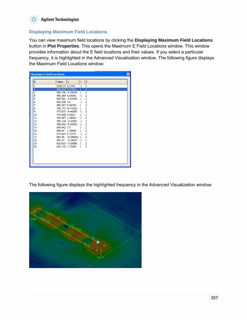
357
Displaying Maximum Field Locations
You can view maximum field locations by clicking the Displaying Maximum Field Locations button in Plot Properties. This opens the Maximum E Field Locations window. This window provides information about the E field locations and their values. If you select a particular frequency, it is highlighted in the Advanced Visualization window. The following figure displays the Maximum Field Locations window:
The following figure displays the highlighted frequency in the Advanced Visualization window:

Electromagnetic
358
Enabling Field Sensors
All the plots are displayed on surfaces. By default, surfaces that are connected to Ports are automatically created and listed in the Sensor Frame.
The Field Sensors region consists of two columns, Show and Enable. The Show check box allows you to display the triangular regions where the field quantities are plotted. The Enable check box allows you to plot the field quantities on that Sensor. The fields that are plotted are determined by the field plotting choices, Shaded, Arrow or Contour.
You can add new sensors by clicking the Add button. There are three different options for adding new sensors:
• Object Plane: You can select a shaded object by clicking on a face. If no object is currently shaded, you should first select an object edge to shade the surface. When an object plane is selected, a plane is defined through the entire design region. In this case, the plane will extend beyond the object definition.
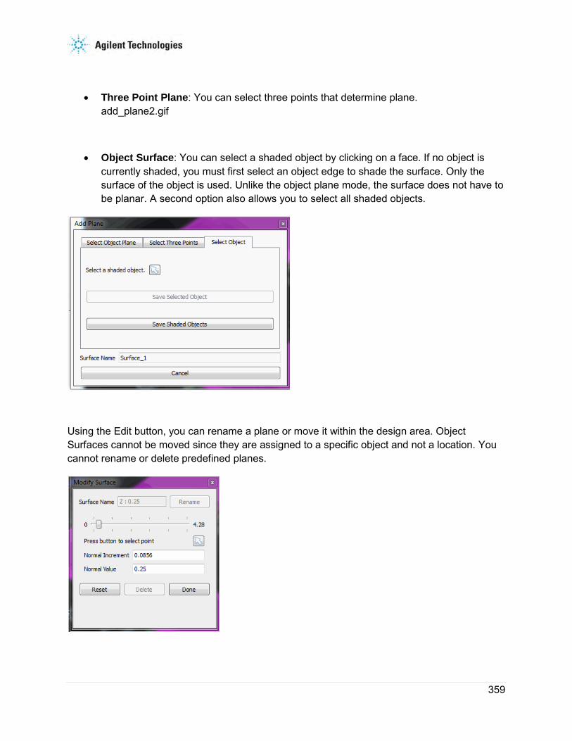
359
• Three Point Plane: You can select three points that determine plane. add_plane2.gif
• Object Surface: You can select a shaded object by clicking on a face. If no object is currently shaded, you must first select an object edge to shade the surface. Only the surface of the object is used. Unlike the object plane mode, the surface does not have to be planar. A second option also allows you to select all shaded objects.
Using the Edit button, you can rename a plane or move it within the design area. Object Surfaces cannot be moved since they are assigned to a specific object and not a location. You cannot rename or delete predefined planes.

Electromagnetic
360
Plotting Properties
Using the Plot Properties tab, you can create the following types of plots:
• Shaded Plot
• Arrow Plot
• Contour Plot
• Volume plot
Displaying a Shaded Plot The shaded plot allows you to plot the magnitude of the field quantity on the sensor surface, as shown in the following figure:
Displaying the shaded current plot is controlled by using the check box next to the plot name. When it is selected, the plot is visible. Within the plot there are some basic controls:
• Log Scale: This controls whether the scaling and color representation uses a logarithmic scale or a linear one.
• Transparency: This controls the transparency of the shaded plot.
Displaying an Arrow Plot The arrow plot allows you to plot the quantity on the sensor surface, as shown in the following figure:

361
After selecting the Arrow tab, select Enable to display the arrow plot. You can control the following properties of an arrow plot:
• Scaling arrows: You can select the Scale check box to control whether the arrows are scaled, based on the relative magnitude of the current density through out the design. When it is selected, the arrows will be scaled, making the lower current density areas have smaller arrows. If it is not selected, all the arrows are displayed with the same size. However, their size can still be changed by changing the arrow size.
• Using a logarithmic scale: You can select the Log Scale check box to control whether the scaling and color representation use a logarithmic scale or a linear one. If scaling is not enabled, only the color weighting is affected.
• Specifying arrow size: You can specify the relative size of the arrow in Arrow Size. Remember that if the arrows are not scaled, the default size of the arrows appear to be larger than when the arrows are scaled.
Displaying a Contour Plot The contour plot allows you to plot the magnitude of the field quantity on the sensor surface, as shown in the following figure:

Electromagnetic
362
After selecting the Contour tab, select Enable to display the contour plot. You can control the following properties of a contour plot:
• Using a logarithmic scale: You can select the Log Scale check box to control whether the scaling and color representation use a logarithmic scale or a linear one. If scaling is not enabled, only the color weighting is affected.
• Specifying the number of divisions: You can specify the number of divisions in the Divisions combo box.
Displaying a Volume Plot The volume plot enables you to scale and specify arrow size, as shown in the following figure:

363
Specifying Plot Options
You can modify the plots by using the options menu. The options menu displays the color key for the plot and can also be used to change the Minimum and Maximum values that are being plotted. The color used for the plot can also be specified from the Options dialog box.

Electromagnetic
364
System Min and System Max: The system minimum and maximum values represent the minimum values for all the plots that are currently being drawn. However, in order to keep scale consistently, the maximum and minimum values are not changed when the Solution Setup is modified. The maximum and minimum values are displayed as System Max and System Min. If you want to use these values instead, click the Restore Max and Min button.
Similarly, you can modify the maximum and minimum values that are used for displaying the data by typing in new values. These will not be changed as the Solution Setup is modified.
X and Y Arrow Density control the density of arrows within a sensor. They have no effect on Object Surface Sensors.
Plotting Boundary Conditions
Use the Boundary Conditions tab in the plotting regions to plot the boundary surfaces. By selecting the Boundaries Visible box, you can pick the boundary surfaces that are visible on the screen. The unassigned surfaces are those which are on the surface of objects, but do not have any boundary conditions assigned to them.
Plotting 3D Mesh
When a solution is loaded, a third column, Mesh, becomes available in the Properties tab. By selecting the Mesh column check box, the mesh inside the material or individual object can now be seen. In some cases, there may not be any mesh inside the object if the object was not assigned any tetrahedral. Flat objects, by definition, do not have any tetrahedral assigned to them.
Shaded Mesh The surface mesh of the objects can be drawn by selecting the Surface Check box in the Mesh box at the bottom of the Properties Tab. Once selected, the volume mesh can also be selected.
Animating FEM Fields
You can animate the FEM fields by selecting the Animate box at the bottom of the Plot Properties Tab. If the Plot Magnitude button is selected, the animation option is not available. X

365
and Y Arrow Density control the density of arrows within a sensor. They have no effect on Object Surface Sensors. You can also change the phase by sliding the Phase Bar, as shown in the following figure:
You can control the following animation options of arrow, shaded, and contour plots:
• Determine the display update time: Specify a value in the Display Update text box to determine the minimal time required between display updates in milliseconds. Since some updates may take longer than this setting, this value is only a minimum number and not an absolute one.
• Determine the Phase Increment value: Specify a value in the Phase Increment text box to control the number of degrees added to the current phase when an update occurs.
8.4 Visualizing Momentum Simulations You can view and analyze the following type of data for Momentum simulations:
• S-parameters
• Currents
• far-fields
• Antenna parameters
• Transmission line data
8.4.1 Starting Momentum Visualization
You must complete the simulation process to view data for a Momentum design. If you have already simulated a design, you can start the Visualization feature directly to view the existing data. Select EM > Post-Processing > Visualization to open the Agilent Momentum

Electromagnetic
366
Visualization window. You can also open this window by clicking Visualization ( ) in the EM toolbar.
To visualize Momentum simulations:
1. Choose EM > Simulation Setup to open the EM Setup window.
2. Select Momentum RF or Momentum Microwave in the EM Setup window.
3. Specify the required settings in the EM Setup window for a layout, substrate, port, frequency plan, output plan, options, resources and model or symbol.
4. Click Simulate in the EM Setup window to simulate your design.
5. Select EM > Post-Processing > Visualization to open the Agilent Momentum Visualization window, as shown in the following figure:
The Agilent Momentum Visualization window appears similar to the EM Previewer window. The initial window layout is similar to that of EM Previewer. The left side contains the basic controls for the view in the docking widget. However, the Agilent Momentum Visualization window includes the following modifications:
• EM Port surfaces are no longer displayed.
• Object shading is removed.
• A shaded current plot for Port 1 at the lowest frequency is displayed.
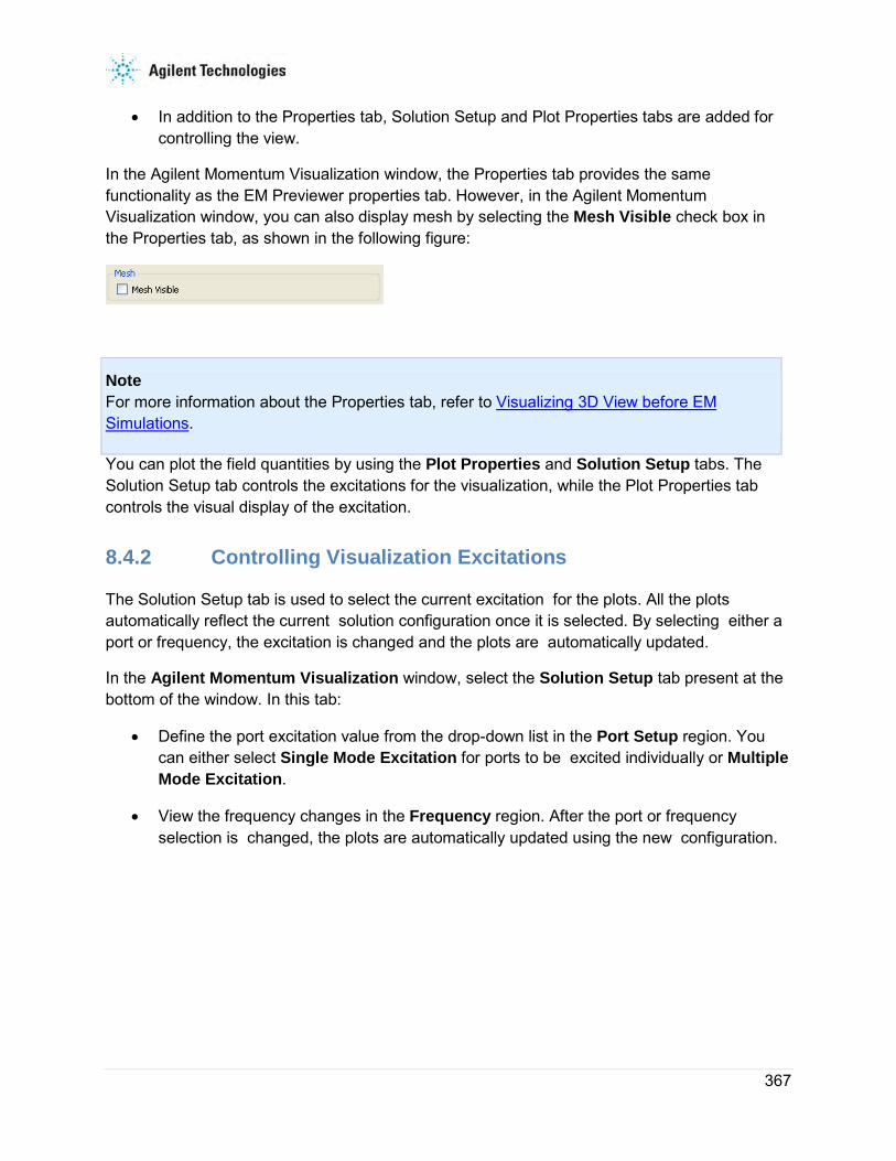
367
• In addition to the Properties tab, Solution Setup and Plot Properties tabs are added for controlling the view.
In the Agilent Momentum Visualization window, the Properties tab provides the same functionality as the EM Previewer properties tab. However, in the Agilent Momentum Visualization window, you can also display mesh by selecting the Mesh Visible check box in the Properties tab, as shown in the following figure:
Note For more information about the Properties tab, refer to Visualizing 3D View before EM Simulations.
You can plot the field quantities by using the Plot Properties and Solution Setup tabs. The Solution Setup tab controls the excitations for the visualization, while the Plot Properties tab controls the visual display of the excitation.
8.4.2 Controlling Visualization Excitations
The Solution Setup tab is used to select the current excitation for the plots. All the plots automatically reflect the current solution configuration once it is selected. By selecting either a port or frequency, the excitation is changed and the plots are automatically updated.
In the Agilent Momentum Visualization window, select the Solution Setup tab present at the bottom of the window. In this tab:
• Define the port excitation value from the drop-down list in the Port Setup region. You can either select Single Mode Excitation for ports to be excited individually or Multiple Mode Excitation.
• View the frequency changes in the Frequency region. After the port or frequency selection is changed, the plots are automatically updated using the new configuration.
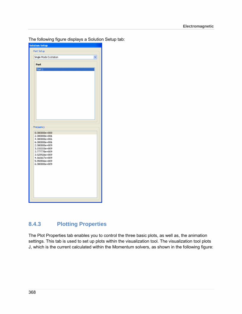
Electromagnetic
368
The following figure displays a Solution Setup tab:
8.4.3 Plotting Properties
The Plot Properties tab enables you to control the three basic plots, as well as, the animation settings. This tab is used to set up plots within the visualization tool. The visualization tool plots J, which is the current calculated within the Momentum solvers, as shown in the following figure:

369
Using the Plot Properties tab, you can create the following types of plots:
• Shaded Plot
• Arrow Plot
• Contour Plot
Displaying a Shaded Plot
Displaying the shaded current plot is controlled by using the check box next to the plot name. When it is selected, the plot is visible. Within the plot there are some basic controls:
• Log Scale - This controls whether the scaling and color representation uses a logarithmic scale or a linear one.
• Transparency - This controls the transparency of the shaded plot.
Displaying an Arrow Plot
After selecting the Arrow tab, select Enable to display the arrow plot. You can control the following properties of an arrow plot:
• Scaling arrows: You can select the Scale check box to control whether the arrows are scaled, based on the relative magnitude of the current density through out the design. When it is selected, the arrows will be scaled, making the lower current density areas

Electromagnetic
370
have smaller arrows. If it is not selected, all the arrows are displayed with the same size. However, their size can still be changed by changing the arrow size.
• Using a logarithmic scale: You can select the Log Scale check box to control whether the scaling and color representation use a logarithmic scale or a linear one. If scaling is not enabled, only the color weighting is affected.
• Specifying arrow size: You can specify the relative size of the arrow in Arrow Size. Remember that if the arrows are not scaled, the default size of the arrows appear to be larger than when the arrows are scaled.
Displaying a Contour Plot
After selecting the Contour tab, select Enable to display the contour plot. You can control the following properties of a contour plot:
• Using a logarithmic scale: You can select the Log Scale check box to control whether the scaling and color representation use a logarithmic scale or a linear one. If scaling is not enabled, only the color weighting is affected.
• Specifying the number of divisions: You can specify the number of divisions in the Divisions combo box.
Modifying Plot Options
You can modify the plots by using the options menu in the Plot Properties tab. The options menu displays the color key for the plot and can also be used to change the Minimum and Maximum values that are being plotted. The color used for the plot can also be specified from the Options dialog box.

371
System Min and System Max: The system minimum and maximum values represent the minimum values for all the plots that are currently being drawn. However, in order to keep scale consistently , maximum and minimum values are not changed when the Solution Setup is modified. The maximum and minimum values are displayed as System Max and System Min. If the user wishes to use these values instead, he can use them by selecting the Restore Max and Min button.
Similarly, the user can modify the maximum and minimum values that are used for displaying the data by typing in new values. These will not be changed as the Solution Setup is modified.
X and Y Arrow Density control the density of arrows within a sensor. They have no effect on Object Surface Sensors.
8.4.4 Animating Momentum Fields
You can animate Momentum fields by selecting Animate at the bottom of the Plot Properties tab. You can also change the phase by sliding the Phase Bar, as shown in the following figure:
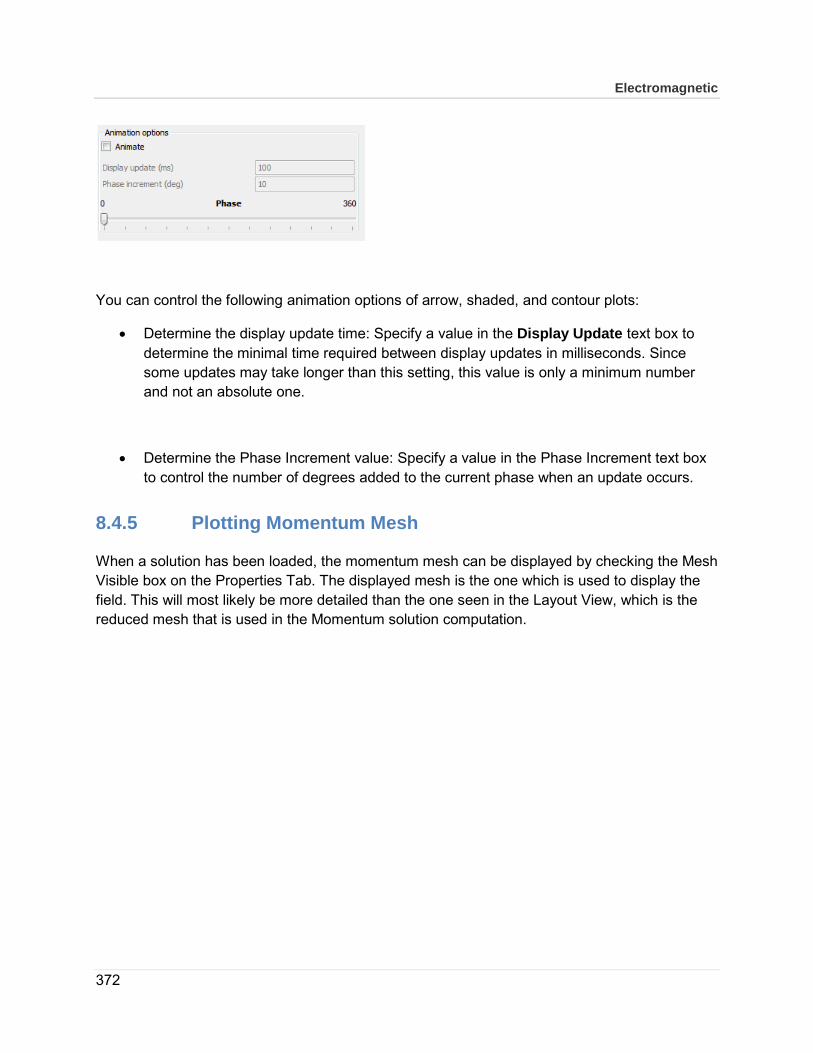
Electromagnetic
372
You can control the following animation options of arrow, shaded, and contour plots:
• Determine the display update time: Specify a value in the Display Update text box to determine the minimal time required between display updates in milliseconds. Since some updates may take longer than this setting, this value is only a minimum number and not an absolute one.
• Determine the Phase Increment value: Specify a value in the Phase Increment text box to control the number of degrees added to the current phase when an update occurs.
8.4.5 Plotting Momentum Mesh
When a solution has been loaded, the momentum mesh can be displayed by checking the Mesh Visible box on the Properties Tab. The displayed mesh is the one which is used to display the field. This will most likely be more detailed than the one seen in the Layout View, which is the reduced mesh that is used in the Momentum solution computation.

373
8.5 Computing Radiation Patterns
This section describes how to calculate the radiation fields. It also provides general information about the antenna characteristics that can be derived based on the radiation fields.
Note In the Momentum RF mode, radiation patterns, and antenna characteristics are not available.
8.5.1 About Radiation Patterns
After calculating currents on the circuit, you can compute the electromagnetic fields. They can be expressed in the spherical coordinate system attached to your circuit. The electric and magnetic fields contain terms that vary as 1/r, and 1/r2. It can be shown that the terms that vary as 1/r 2, and 1/r 3 are associated with the energy storage around the circuit. They are called the reactive field or near-field components. The terms having a 1/r dependence become dominant at large distances and represent the power radiated by the circuit. These terms are called far field components (Eff, Hff).

Electromagnetic
374
In a layout, there is a fixed coordinate system such that the monitor screen lies in the XY-plane. The X-axis is horizontal, the Y-axis is vertical, and the Z-axis is normal to the screen.
Note In the direction parallel to the substrate (theta = 90 degrees), parallel plate modes or surface wave modes, that vary as 1/sqrt(r), are also present. Although the modes dominate in this direction, they are not considered to be part of the far-fields.
The radiated power is a function of the angular position and the radial distance from the circuit. The variation of power density with angular position is determined by the type and design of the circuit. It can be graphically represented as a radiation pattern.
The far-fields can only be computed at those frequencies that were calculated during a simulation. The far-fields will be computed for a specific frequency and for a specific excitation state. They will be computed in all directions (theta, phi) in the open half space above and/or below the circuit. Besides the far-fields, derived radiation pattern quantities such as gain and axial ratio are computed.
Note It is possible to calculate far-fields for some designs that have a top or bottom layer that is not defined as open space.

375
8.5.2 About Antenna Characteristics
Based on the far fields, you can derive polarization and other antenna characteristics such as gain and radiated power.
Polarization
The far-field can be decomposed in several ways. You can work with the basic decomposition in ( , ). However, with linear polarized antennas, it is sometimes more convenient to decompose the far-fields into (Eco, Ecross) which is a decomposition based on an antenna measurement set-up. For circular polarized antennas, a decomposition into left and right hand polarized field components (Elhp, Erhp) is most appropriate. Below you can find how the different components are related to each other.
is the characteristic impedance of the open half sphere under consideration.
The fields can be normalized with respect to:

Electromagnetic
376
Circular Polarization The following figures displays the left hand and right hand circular polarized field components are derived.
Using these equation, you can calculate the circular polarization axial ratio (ARcp). The axial ratio describes how well the antenna is circular polarized. If its amplitude equals one, the fields are perfectly circularly polarized. It becomes infinite when the fields are linearly polarized.
Linear Polarization Below, the equations to decompose the far-fields into a co and cross polarized field are given (
is the co polarization angle).
Using these equations, you can calculate the linear polarization axial ratio (ARlp). This value illustrates how well the antenna is linearly polarized. It equals to one when perfect linear polarization is observed and becomes infinite for a perfect circular polarized antenna.
Note
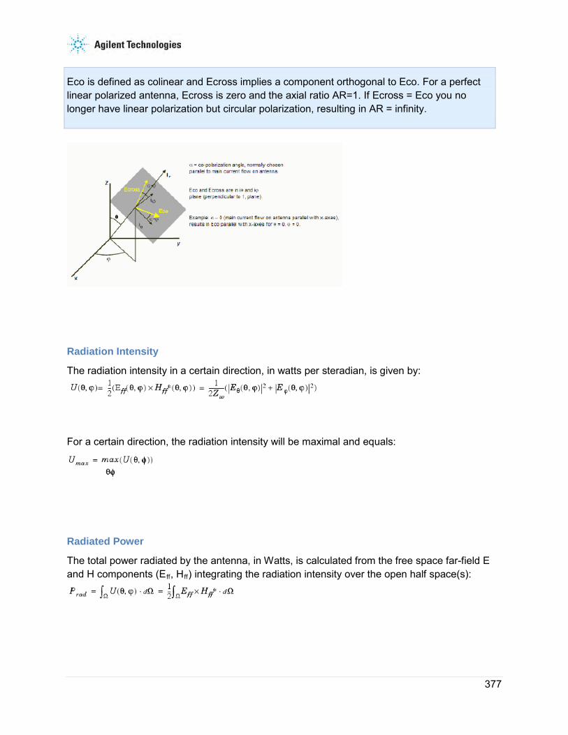
377
Eco is defined as colinear and Ecross implies a component orthogonal to Eco. For a perfect linear polarized antenna, Ecross is zero and the axial ratio AR=1. If Ecross = Eco you no longer have linear polarization but circular polarization, resulting in AR = infinity.
Radiation Intensity
The radiation intensity in a certain direction, in watts per steradian, is given by:
For a certain direction, the radiation intensity will be maximal and equals:
Radiated Power
The total power radiated by the antenna, in Watts, is calculated from the free space far-field E and H components (Eff, Hff) integrating the radiation intensity over the open half space(s):

Electromagnetic
378
Note The power going into the surface wave is not taken into account in this calculation.
Effective Angle
This parameter is the solid angle through which all power emanating from the antenna would flow if the maximum radiation intensity is constant for all angles over the beam area. It is measured in steradians and is represented by:
Directivity
Directivity calculates the radiation intensity in a certain direction versus the radiated power. Directivity is dimensionless and calculated by using the following equation:
Directivity indicates the best you could get out of the antenna. In reality, there will be loss mechanisms in the antenna (see Gain) and the feed network is never perfectly matched. The maximum directivity is given by:
Gain
Gain looks at radiation intensity in a certain direction versus the power injected into the antenna. The gain of the antenna is calculated as:
where Pinj is the real power, in watts, injected into the circuit. The injected power, or net input power, equals to the (incident - reflected) power at the port(s). Consequently, the impact of

379
mismatch is not included in this definition of Gain. For a good antenna, a large part of the injected power is radiated, the rest will be lost. The loss is due to the presence of lossy materials (either the conductors or the dielectrics used) or gets trapped into the surface wave that propagates cylindrically along the substrate plane.
The injected power is calculated from the S-parameters and the excitation sources (Thevenin sources) at the ports as specified by the user. In case of a 1-port antenna, the excitation source specified by the user doesn't really matter since both Directivity and Gain are normalized values. For a multi-port antenna, the exact source excitation setup at each port is really important. That is where the far field excitation utility available from the knowledge center (search for Far Field Computations from AC/HB Analysis of Antennas Plus Circuitry) is very relevant.
The maximum gain is given by:
Efficiency
The efficiency is given by:
Effective Area
The effective area, in square meters, of the antenna circuit is given by:
8.5.3 Calculating Far Fields
To calculate far fields:
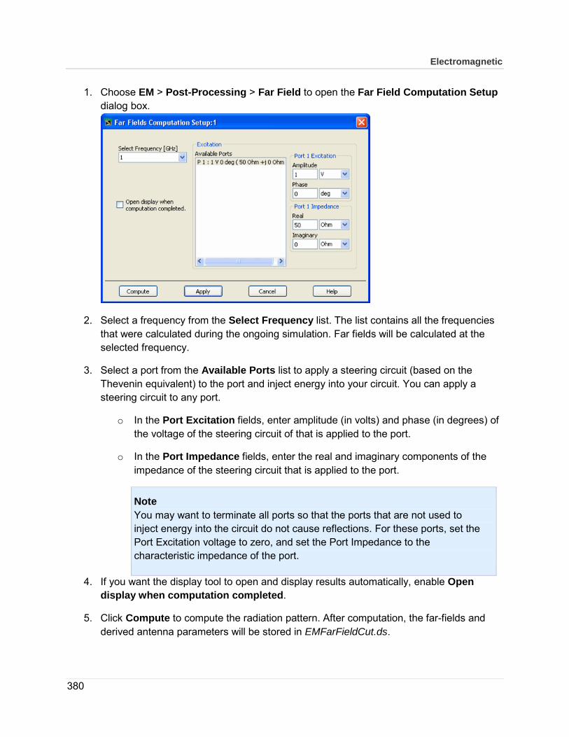
Electromagnetic
380
1. Choose EM > Post-Processing > Far Field to open the Far Field Computation Setup dialog box.
2. Select a frequency from the Select Frequency list. The list contains all the frequencies that were calculated during the ongoing simulation. Far fields will be calculated at the selected frequency.
3. Select a port from the Available Ports list to apply a steering circuit (based on the Thevenin equivalent) to the port and inject energy into your circuit. You can apply a steering circuit to any port.
o In the Port Excitation fields, enter amplitude (in volts) and phase (in degrees) of the voltage of the steering circuit of that is applied to the port.
o In the Port Impedance fields, enter the real and imaginary components of the impedance of the steering circuit that is applied to the port.
Note You may want to terminate all ports so that the ports that are not used to inject energy into the circuit do not cause reflections. For these ports, set the Port Excitation voltage to zero, and set the Port Impedance to the characteristic impedance of the port.
4. If you want the display tool to open and display results automatically, enable Open display when computation completed.
5. Click Compute to compute the radiation pattern. After computation, the far-fields and derived antenna parameters will be stored in EMFarFieldCut.ds.
381
8.5.4 Viewing Far Fields
After the far fields computations are performed, data is saved depending on the display tool. The following types of displays are used:
• 2D Data Display: Data is stored in the EMFarFieldCut.ds file.
• 3D Visualization: Far-fields and derived antenna parameters will be stored in respectively proj.fff and proj.ant in the <workspace>/simulation/<library>/<cell>/layout/emSetp_MoM/ directory of your workspace. The antenna parameters are also saved in the dataset EMFarFieldCut.ds.
Viewing Far Fields in 3D Visualization
When 3D Visualization is selected as Visualization Type for viewing the far-field results, the 3D Visualization Tool is automatically displayed when the computation is finished. Two windows are displayed, a Geometry window and a Far Field window. The Far Field Window and associated properties tab is only shown if radiation results are available. The radiation results are for a single frequency, shown on the properties tab, and using the excitation state as specified in the Radiation Pattern Control dialog box before computation. A new Visualization window can be opened when far fields are calculated at another frequency.
Note The Solution Setup and Plot Properties tabs have no association with the Far Field window. They apply to the surface current visualization on the Geometry window.

Electromagnetic
382
Select the Plot type:
• E = sqrt(mag(E Theta)2 + mag(E Phi)2)
• E Theta
• E Phi
• E Left
• E Right
• E Co
• E Cross
• Circular Axial Ratio
• Linear Axial Ratio
If you want the data normalized to a value of one, enable Normalize. For Circular and Linear Axial Ratio choices, set the Minimum dB. Also set the Polarization Angle for E Co, E Cross, and Linear Axial Ratio. By default, a logarithmic scale is used to display the plot. If you want to use a linear scale, disable Log scale. Set the minimum magnitude that you want to display, in dB.

383
Click Antenna Parameters to view gain, directivity, radiated power, maximum E-field, and direction of maximum radiation.
The data is based on the frequency and excitation state as specified in the Radiation Pattern Control dialog. The parameters include:
• Radiated power, in watts
• Effective angle, in degrees
• Directivity, in dB
• Gain, in dB
• Maximum radiation intensity, in watts per steradian
• Direction of maximum radiation intensity, theta and phi, both in degrees
• E_theta, magnitude in Volt and phase in degrees in direction of maximum radiation
• E_phi, magnitude in Volt and phase in degrees in direction of maximum radiation
• E_x, magnitude in Volt and phase in degrees in direction of maximum radiation
• E_y, magnitude in Volt and phase in degrees in direction of maximum radiation
• E_z, magnitude in Volt and phase in degrees in direction of maximum radiation
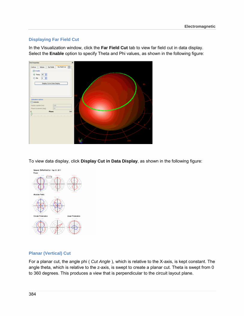
Electromagnetic
384
Displaying Far Field Cut
In the Visualization window, click the Far Field Cut tab to view far field cut in data display. Select the Enable option to specify Theta and Phi values, as shown in the following figure:
To view data display, click Display Cut in Data Display, as shown in the following figure:
Planar (Vertical) Cut
For a planar cut, the angle phi ( Cut Angle ), which is relative to the X-axis, is kept constant. The angle theta, which is relative to the z-axis, is swept to create a planar cut. Theta is swept from 0 to 360 degrees. This produces a view that is perpendicular to the circuit layout plane.
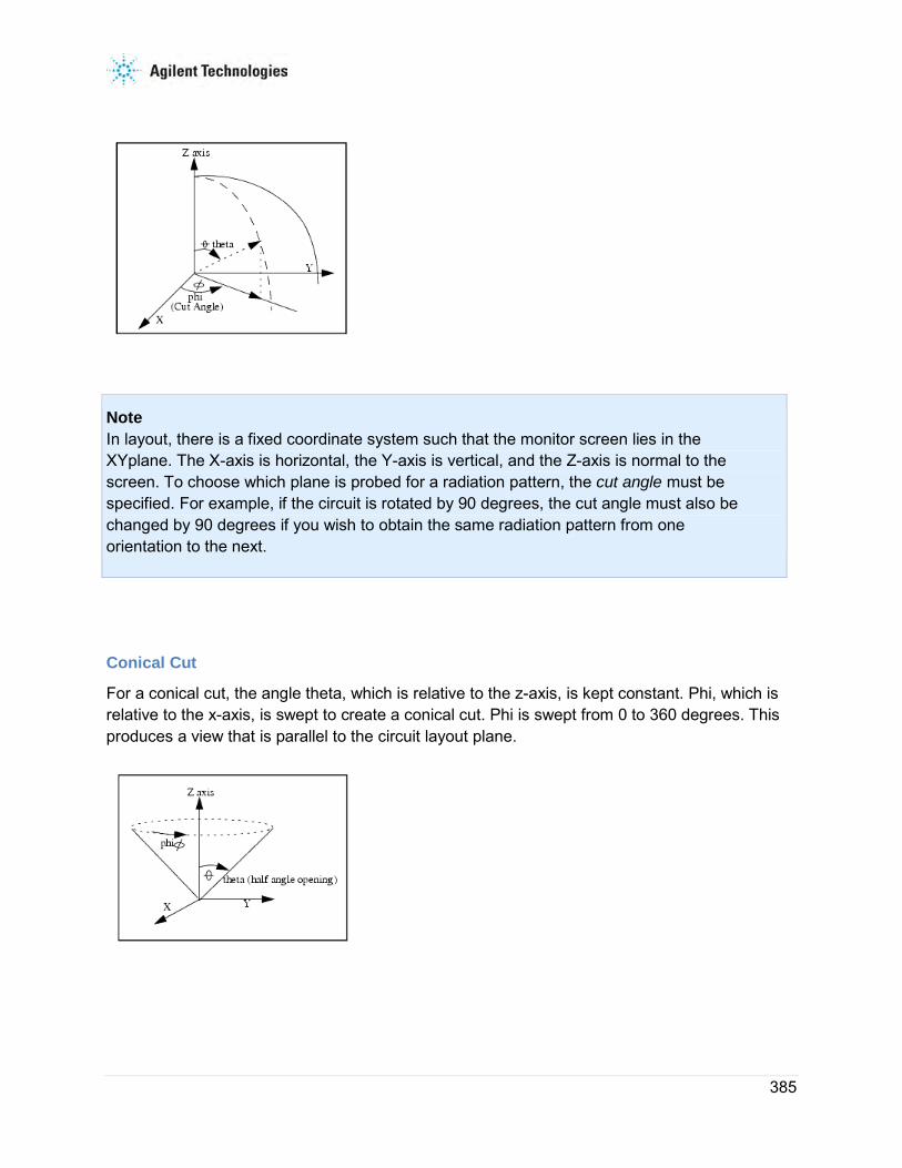
385
Note In layout, there is a fixed coordinate system such that the monitor screen lies in the XYplane. The X-axis is horizontal, the Y-axis is vertical, and the Z-axis is normal to the screen. To choose which plane is probed for a radiation pattern, the cut angle must be specified. For example, if the circuit is rotated by 90 degrees, the cut angle must also be changed by 90 degrees if you wish to obtain the same radiation pattern from one orientation to the next.
Conical Cut
For a conical cut, the angle theta, which is relative to the z-axis, is kept constant. Phi, which is relative to the x-axis, is swept to create a conical cut. Phi is swept from 0 to 360 degrees. This produces a view that is parallel to the circuit layout plane.

Electromagnetic
386
8.5.5 Exporting Far Field Data
ASCII file with 3D Far Field Data
If 3D Visualization is selected in the Radiation Pattern dialog, the normalized electric far-field components for the complete hemisphere are saved in ASCII format in the file < workspace_dir>/mom_dsn/<design_name>/proj.fff. The data is saved in the following format:
#Frequency <f> GHz // loop over frequencies #Excitation # <i> // loop over excitation states #---------------- #Begin cut // loop over phi <theta_0> <phi_0> <real(E_theta)> <imag(E_theta)> <real(E_phi)> <imag(E_phi)> // loop over <theta> for <phi_0> <theta_1> <phi_0> <real(E_theta)> <imag(E_theta)> <real(E_phi)> <imag(E_phi)> : <theta_n> <phi_0> <real(E_theta)> <imag(E_theta)> <real(E_phi)> <imag(E_phi)> #End cut #Begin cut <theta_0> <phi_1> <real(E_theta)> <imag(E_theta)> <real(E_phi)> <imag(E_phi)> // loop over <theta> for <phi_1> <theta_1> <phi_1> <real(E_theta)> <imag(E_theta)> <real(E_phi)> <imag(E_phi)> : <theta_n> <phi_1> <real(E_theta)> <imag(E_theta)> <real(E_phi)> <imag(E_phi)> #End cut : : #Begin cut <theta_0> <phi_n> <real(E_theta)> <imag(E_theta)> <real(E_phi)> <imag(E_phi)> // loop over <theta> for <phi_n> <theta_1> <phi_n> <real(E_theta)> <imag(E_theta)> <real(E_phi)> <imag(E_phi)> : <theta_n> <phi_n> <real(E_theta)> <imag(E_theta)> <real(E_phi)> <imag(E_phi)> #End cut
In the proj.fff file, E_theta and E_phi represent the theta and phi components, respectively, of the far-field values of the electric field. Note that the fields are described in the spherical co-ordinate system (r, theta, phi) and are normalized. The normalization constant for the fields can be derived from the values found in the proj.ant file and equals:
with E_theta_max and E_phi_max respectively the E_theta and E_phi in the direction of maximum radiation intensity.

387
ASCII file with Antenna Characteristics
The proj.ant file, stored in the same directory, contains the antenna characteristics. The data is saved in the following format:
Excitation <i> // For Momentum, a single excitation state is specified in the Radiation Pattern Control dialog, consequently <i> is always 1. Frequency <f> GHz // For Momentum, a single frequency is selected in the Radiation Pattern Control dialog Maximum radiation intensity <U> // in Watts/steradian Angle of U_max <theta> <phi> // both in deg E_theta_max <mag(E_theta_max)> ; E_phi_max <mag(E_phi_max)> E_theta_max <real(E_theta_max)> <imag(E_theta_max)> E_phi_max <real(E_phi_max)> <imag(E_phi_max)> Ex_max <real(Ex_max)> <imag(Ex_max)> Ey_max <real(Ey_max)> <imag(Ey_max)> Ez_max <real(Ez_max)> <imag(Ez_max)> Power radiated <i> <prad> // in Watts Effective angle <eff_angle_st> steradians <eff_angle_deg> degrees Directivity <dir> dB // in dB (10*log10) Gain <gain> dB // in dB (10*log10)
The maximum electric field components (E_theta_max, E_phi_max, etc.) are those found at the angular position where the radiation intensity is maximal. They are all in volts.
Dataset file with 2D Cut Far Field Data
Specific information about the data available in the far-field dataset is given in this section.
Variable Description THETA
The swept parameter of a planar cut. When THETA is swept, PHI is at a fixed angle specified in the Cut Angle field and is not returned to the dataset.
PHI
The swept parameter of a conical cut. When PHI is swept, THETA is at a fixed angle specified in the Cut Angle field and is not returned to the dataset.
Etheta and Ephi
Absolute field strength (in volts) of the theta and phi electric far-field components.
Htheta and Hphi
Absolute field strength (in amperes) of the theta and phi magnetic far-field components.
Elhp and Erhp
Normalized field strength of respectively left-hand and right-hand circular polarized electric far-field component.

Electromagnetic
388
Variable Description ARcp
Axial ratio, derived from left-hand and right-hand circular polarized far-field components.
Eco and Ecross
Normalized field strength of co and cross polarized electric far-field components.
ARlp
Linear polarization axial ratio, derived from co and cross polarized far-field components.
Gain, Directivity, Efficiency, EffectiveArea
Gain, Directivity, Efficiency (in percent), Effective area (in m2).
Power
Radiation intensity (in watts/steradian).
Note The normalized far-field components (Elhp, Erhp, Eco, and Ecross) are normalized with
respect to .
8.6 Viewing Simulation Summary During a simulation process, you can view the statistics of momentum mesh, S parameter, substrate, mesh, and geometry statistics. The simulation summary includes time to solve, the resources required, cell information, and any messages that were displayed in the status window. You can view the following types of summary for an EM simulation:
• Momentum mesh
• S-param simulation summary
• Mesh generation summary
• Geometry preproc summary
• Substrate generation summary
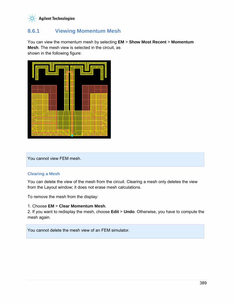
389
8.6.1 Viewing Momentum Mesh
You can view the momentum mesh by selecting EM > Show Most Recent > Momentum Mesh. The mesh view is selected in the circuit, as shown in the following figure:
You cannot view FEM mesh.
Clearing a Mesh
You can delete the view of the mesh from the circuit. Clearing a mesh only deletes the view from the Layout window; it does not erase mesh calculations.
To remove the mesh from the display:
1. Choose EM > Clear Momentum Mesh. 2. If you want to redisplay the mesh, choose Edit > Undo. Otherwise, you have to compute the mesh again.
You cannot delete the mesh view of an FEM simulator.
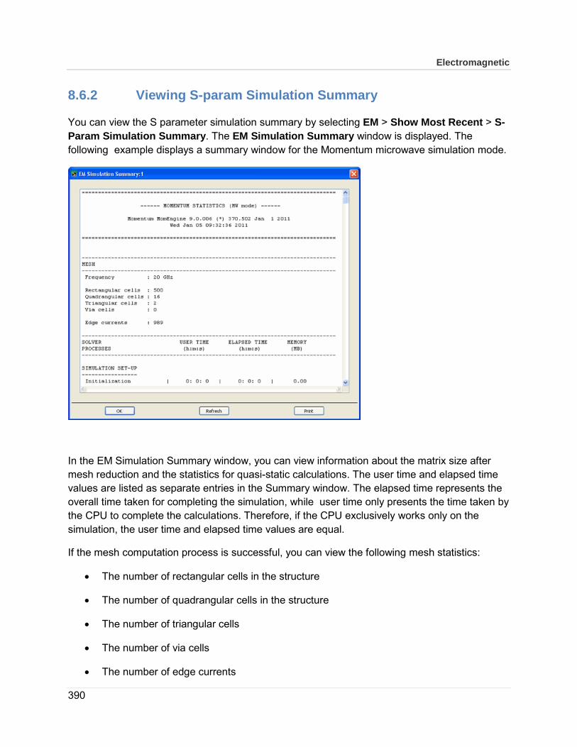
Electromagnetic
390
8.6.2 Viewing S-param Simulation Summary
You can view the S parameter simulation summary by selecting EM > Show Most Recent > S-Param Simulation Summary. The EM Simulation Summary window is displayed. The following example displays a summary window for the Momentum microwave simulation mode.
In the EM Simulation Summary window, you can view information about the matrix size after mesh reduction and the statistics for quasi-static calculations. The user time and elapsed time values are listed as separate entries in the Summary window. The elapsed time represents the overall time taken for completing the simulation, while user time only presents the time taken by the CPU to complete the calculations. Therefore, if the CPU exclusively works only on the simulation, the user time and elapsed time values are equal.
If the mesh computation process is successful, you can view the following mesh statistics:
• The number of rectangular cells in the structure
• The number of quadrangular cells in the structure
• The number of triangular cells
• The number of via cells
• The number of edge currents

391
• Simulation setup information
For an FEM simulation, you can view information about the frequency, meshing time, and simulation time. The following figure displays the S-param summary for an FEM simulation:
8.6.3 Viewing Mesh Generation Summary
You can view the generated mesh statistics by selecting EM > Show Most Recent > Mesh Generation Summary. The Mesh Summary window is displayed. The following example

Electromagnetic
392
displays the summary window for the Momentum microwave simulation mode.
In the Mesh Summary window, you can view the following mesh statistics:
• Number of Quadrilateral cells
• Number of triangular cells
• Number of via cells
• Number of edge currents
• Computer resources used and time to solve
• User Time and Elapsed Time
8.6.4 Viewing Geometry Preproc Summary
You can view the layout processing report by selecting EM > Show Most Recent > Geometry Preproc Summary. The Layout Processing Report window is displayed. The following example displays a summary window for the Momentum microwave simulation mode:

393
This summary window provides information about the minimum snap distance used for layout healing and frequency of mesh generation.
8.6.5 Viewing Substrate Generation Summary
You can view the substrate summary by selecting EM > Show Most Recent > Substrate Generation Summary. This displays the Substrate Summary window. The following example displays a summary window for the Momentum microwave simulation mode:

Electromagnetic
394
This summary window provides information about the process size, user time, and elapsed time.
The FEM simulator does not provide any substrate summary information.

395
Chapter 9 – EM Circuit Cosimulation • Using an EM Model
• Defining Component Parameters
• Performing EM Circuit Cosimulation
• Using the EM Circuit Excitation AEL Addon
9.1 Using an EM Model
An EM Model is used by a circuit simulator to model a component by using the S-parameters generated by an EM simulation. The EM-based S-parameters can be precomputed or you can generate them while running the circuit simulation. An EM Model caches the S-parameters to improve performance. EM Models are compatible with Dynamic Model Selection, which enables you to switch between two different models for the same cell. For example, a faster, schematic-based representation, and an accurate EM-based representation.
Note In ADS 2009 Update 1 and earlier, a Layout Component is used instead of an EM Model. For more information, refer Layout Components and EM Models.
9.1.1 Creating an EM Model
To create an EM model:
1. Choose EM > Simulation Setup to open the EM Setup window.
2. Select Model/Symbol in the left pane of the EM Setup window.
3. Click Create EM model when simulation is launched to create an EM model after the simulation process.
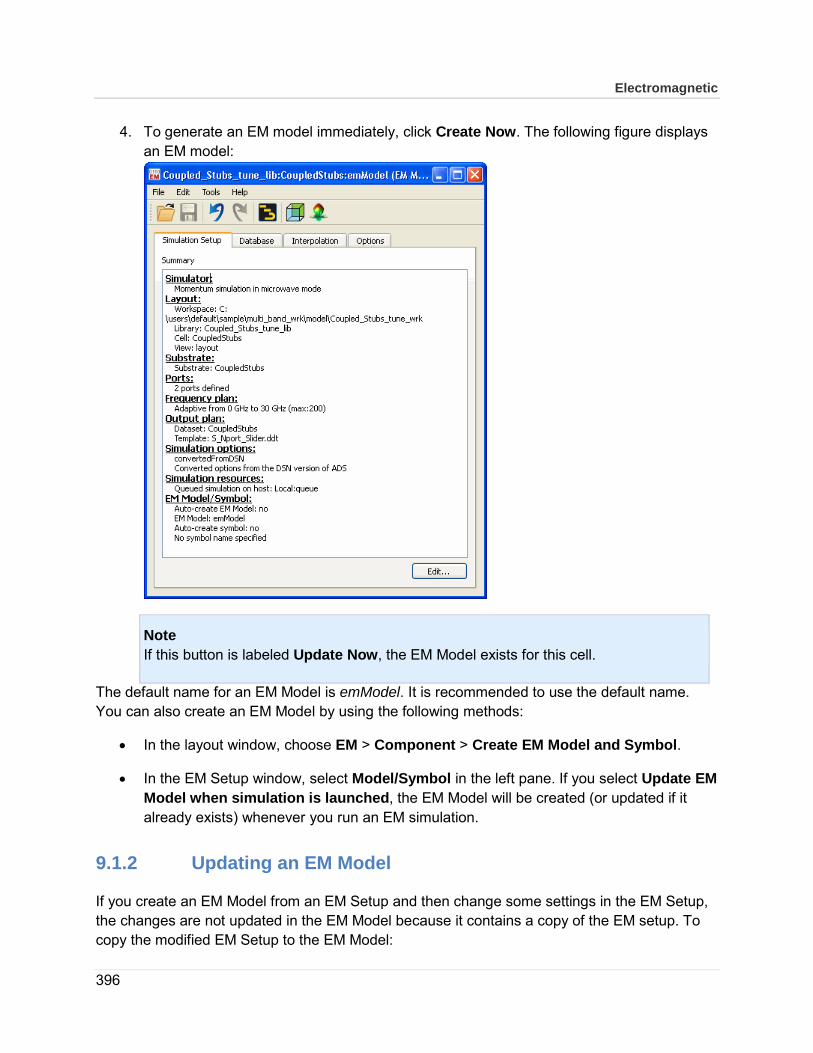
Electromagnetic
396
4. To generate an EM model immediately, click Create Now. The following figure displays an EM model:
Note If this button is labeled Update Now, the EM Model exists for this cell.
The default name for an EM Model is emModel. It is recommended to use the default name. You can also create an EM Model by using the following methods:
• In the layout window, choose EM > Component > Create EM Model and Symbol.
• In the EM Setup window, select Model/Symbol in the left pane. If you select Update EM Model when simulation is launched, the EM Model will be created (or updated if it already exists) whenever you run an EM simulation.
9.1.2 Updating an EM Model
If you create an EM Model from an EM Setup and then change some settings in the EM Setup, the changes are not updated in the EM Model because it contains a copy of the EM setup. To copy the modified EM Setup to the EM Model:
397
1. Choose EM > Simulation Setup to open the EM Setup window.
2. Select Model/Symbol in the left pane of the EM Setup window.
3. Click Update Now in the EM Model panel.
Note If this button is labeled as Create Now, then the EM Model does not exist for that cell.
When you update an EM Model and this causes the EM Model setup to change in a way that affects the EM simulation results, the system deletes all the cached EM results. See The EM Model database for more information.
You can also update an EM Model by using the following methods:
• In the layout window, choose EM > Component > Create EM Model and Symbol.
• In the EM Setup window, on the Model/Symbol page, check Update EM Model when simulation is launched. With this checked, every time you run an EM simulation using this EM Setup, the EM Model will be updated (or created if it does not exist). Using an EM Model for circuit simulation.
9.1.3 Using an EM Model for Circuit Simulation
Default View used by a Circuit Simulation
By default, the view named schematic is used by ADS circuit simulation before a view named emModel. Therefore, if you insert an instance of a cell that has an EM Model view named emModel, there are two possibilities:
• If the cell has no view named schematic, then the EM Model view named emModel is used for circuit simulation.
• If the cell has a view named schematic, the EM Model view is not used for circuit simulation. Instead, the view named schematic is used.
You can change the default behavior by using Dynamic Model Selection. For more information, refer Dynamic Model Selection.
To find the view that is used for an instance during circuit simulation, open the top-level schematic and choose Simulate > Hierarchy Explorer. In the Hierarchy Explorer dialog box, find the instance name in the Instance column. Then search in the View for Simulation column to find the view that is used for circuit simulation. If the view for simulation is not emModel, you need to specify the system to use emModel.
Electromagnetic
398
Specifying an EM Model for Circuit Simulation
To specify the view to be used for a circuit simulation:
1. Select the instance on the schematic.
2. Click the Choose View for Simulation toolbar button, immediately to the left of the Simulate toolbar button. This dialog box lists all the views available for circuit-simulation for the cell associated with this instance.
3. Select the view named emModel.
4. Click OK. The circuit simulator uses the view named emModel for this instance.
The view name emModel is now displayed on the instance. This is a quick way to tell whether a specific view has been chosen for an instance. You can use the Hierarchy Explorer (choose Simulate > Hierarchy Explorer in the top-level schematic) to verify that this change has taken effect.
If you specify emModel in the Choose View for Simulation dialog box, but the Hierarchy Explorer shows that emModel is not the view that is used for circuit simulation, the top-level schematic is using a hierarchy policy that has the Honor instance specializations option selected.
9.1.4 EM Model Window Overview
When an EM Model is created from an EM Setup window, all the settings specified in the EM setup window are copied to the EM Model. Later, during a circuit simulation, if the EM Model needs to run an EM simulation to generate on-demand S-parameters, this copy of the settings is used to launch the EM simulation.
The EM Model window consists of four tabs: Simulation Setup, Database, Interpolation, and Options. The following sections describe the tasks that you can perform using these tabs.
Viewing Simulation Setup Summary
You can view a summary of your EM simulation setup in the Simulation Setup tab. This tab provides information about the type of simulator, layout, substrate, ports defined for your simulation, frequency and output plans, simulation options and resources, and EM model and symbol information.

399
You can view the EM setup details and modify the setup by clicking Edit.
Note When you change the value of a simulation option that affects the EM simulation results, the system deletes EM results cached in the EM Model.
The EM Model Database
To improve circuit simulation performance, each EM Model maintains a database of the EM simulation results. When a circuit simulator requests S-parameters from the EM Model, an EM simulation is performed only when the S-parameters are not available in the database. If an EM simulation is performed, the results are added to the database.
Any change that affects the EM simulation results causes an EM Model database to become out of date. Examples of this type of changes are:
• EM Model simulation setup changes: For example, changing the mesh density.

Electromagnetic
400
• Changes to the cell parameter set: Adding a parameter to the cell or deleting a parameter from the cell.
• Substrate changes: For example, changing the thickness of a metal layer in the substrate.
• Layout changes: For example, adding shapes or components to the layout.
The EM model automatically detects changes to the EM Model and changes to the cell parameter set. When such a change is detected, the EM Model automatically deletes its database. However, other changes are not automatically detected. If you make such a change, you should open the EM Model, access the Database tab and click Delete All.
Specifying Cell Parameter Interpolation Options
The settings on the Interpolation tab are used by the circuit simulator to determine whether for a given set of cell parameter values, model data is available, can be constructed by interpolation, or if a new EM simulation is required. In the absence of a unit name, MKS units are assumed.
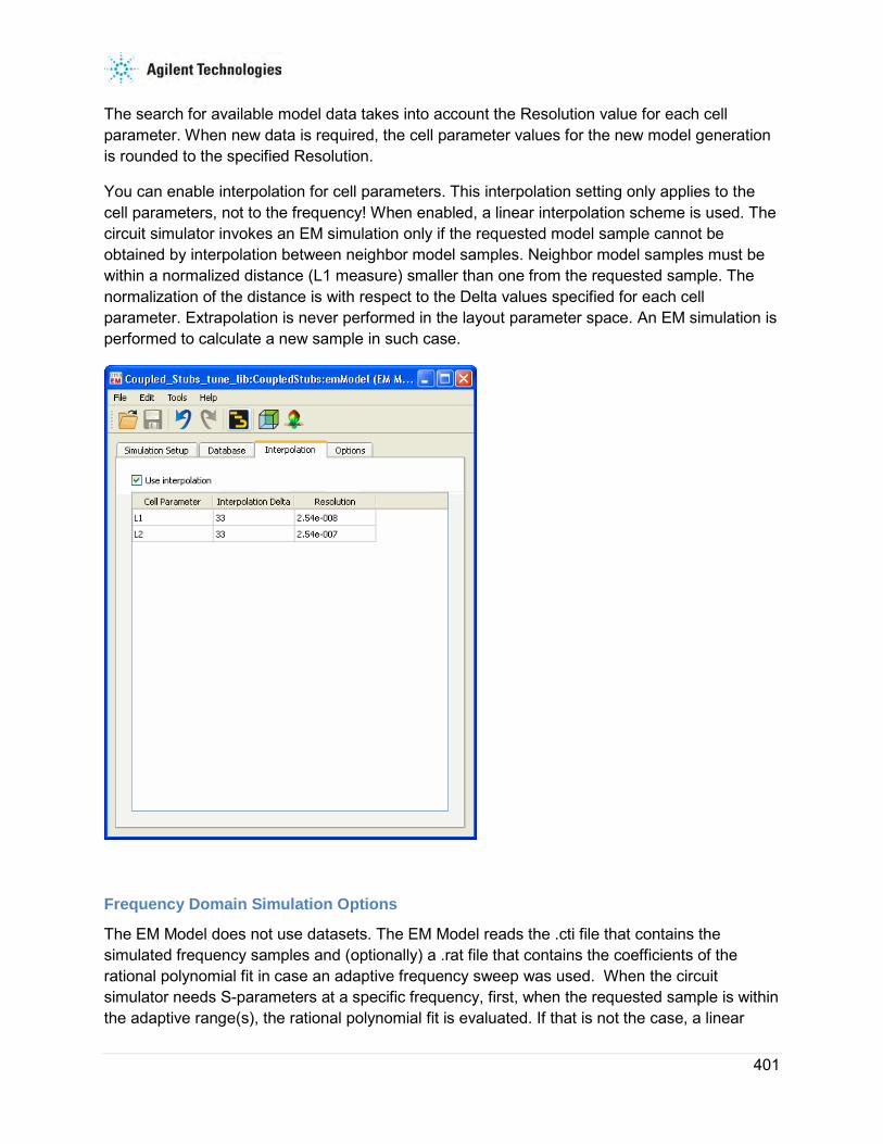
401
The search for available model data takes into account the Resolution value for each cell parameter. When new data is required, the cell parameter values for the new model generation is rounded to the specified Resolution.
You can enable interpolation for cell parameters. This interpolation setting only applies to the cell parameters, not to the frequency! When enabled, a linear interpolation scheme is used. The circuit simulator invokes an EM simulation only if the requested model sample cannot be obtained by interpolation between neighbor model samples. Neighbor model samples must be within a normalized distance (L1 measure) smaller than one from the requested sample. The normalization of the distance is with respect to the Delta values specified for each cell parameter. Extrapolation is never performed in the layout parameter space. An EM simulation is performed to calculate a new sample in such case.
Frequency Domain Simulation Options
The EM Model does not use datasets. The EM Model reads the .cti file that contains the simulated frequency samples and (optionally) a .rat file that contains the coefficients of the rational polynomial fit in case an adaptive frequency sweep was used. When the circuit simulator needs S-parameters at a specific frequency, first, when the requested sample is within the adaptive range(s), the rational polynomial fit is evaluated. If that is not the case, a linear

Electromagnetic
402
interpolation is tried using the .cti file samples. If that is not possible, a linear extrapolation with passivity enforcement is done. In case of a non-adaptive sweep, the frequency domain interpolation is always linear using the samples that were simulated from the .cti file. Within an adaptive range, the rational polynomial fit is evaluated. There is no control over the interpolation.
You can specify the following frequency domain simulation options:
Extrapolation mode: You can specify the following values for the extrapolation mode:
• Linear (default): A linear extrapolation scheme is used for both magnitude and phase. By default, passivity of the S-parameter model is enforced during extrapolation.
• Constant: The S-parameters at the lowest or highest available frequency are used.
• Exponential e-damping: A mixed extrapolation scheme is used. S-parameters at kept constant during extrapolation towards low frequencies. Towards high frequencies, S-parameters are e-damped in magnitude and linearly extrapolated versus phase.
Enforce passivity: The passivity of the S-parameter model can be enforced. You can enable or disable passivity enforcement through the Enforce Passivity parameter. You can specify the following values for enforce passivity:
• Only when extrapolating: S-parameter model passivity is enforced only during frequency domain extrapolation.
• Always: S-parameter model passivity is enforced at all frequencies.
• Never: S-parameter model passivity is not enforced.
Netlist Options

403
The Multi-pins port terminal setting is only relevant when S-parameter ports were defined having multiple layout pins connected to either the plus or minus terminal, or both. The symbol consists of similar number of pins as that in the layout.
• Use shorts in netlist: convenience setting that shorts all pins connected to the S-parameter port terminal in the netlist fragment for the EM Model. It is sufficient to connect/wire to one symbol pin only.
• Use transformers in netlist: transformers is used in the netlist fragment for the EM Model to extract the common mode voltage and current from the multiple pins. This option is required when the pins cannot be shorted automatically.
Tools Menu
The Tools menu in the EM Model provides following capabilities:
• Open Layout Window opens the corresponding layout cell view in a Layout window. For a cell with parameters, this is the 'nominal' layout view with default parameter values.
• Far Field allows you to compute the far field for the selected data item in the EM Model database.
• Visualization opens the 3D Visualization window for the selected data item in the EM Model database.
Far Field and/or Visualization driven from an EM Model is not possible when the EM Model was generated with the 'Include S parameter data only' flag enabled in the corresponding EM Setup. The following warning window is displayed:
Disabling the flag ensures that all data required for post-processing operations are stored with the EM Model. Changing the flag in the EM Setup and updating the EM Model does not invalidate existing EM Model data. The flag will only take effect for newly generated data samples. If you want to do post-processing operation on existing EM Model data items, delete and regenerate them.
Note Far-field computation and 3D Visualization driven from the EM Model database is only possible for simple EM Model data items, not for the scalable model data items that the

Electromagnetic
404
Advanced Model Composer generates. The scalable model data can be recognized by the LIST or RANGE parameter values. Data for post-processing cannot be stored in the EM Model database because such EM Model data item spans a (discrete or continuous) range of instances of a parametric layout.
9.2 Defining Component Parameters You can create user-defined components from a layout window in ADS. You can insert these components in a schematic window just like any other component, and represents the (parametric) layout from the layout page. The symbol representing this component in schematic can either be a black box or a layout look-alike symbol. You can also create an EM Model to model a component by using the S-parameters generated by an EM simulation.
After creating a component, you can use it in one of the following ways:
• You can directly include the component in a schematic. During circuit simulation from the schematic environment, a solver is called automatically to generate a model. The user-defined layout parameters and the relevant simulation parameters (e.g., model type, mesh density) can be set from the schematic page. The EM model consists of a built-in database mechanism that stores previously calculated Momentum simulation results. Therefore, after Momentum simulation is done for a certain layout component, no new EM simulations are required, unless there is a change in the parameters for this component.
• You can use the components as the starting point of Advanced Model Composer (AMC), for more details see Using Advanced Model Composer. AMC is a generalization of Model Composer, for details see Model Composer, enabling you to generate a parameterized electrical model for a Component from within the layout window. After defining and creating the component, you can specify the ranges for the parameters (with continuous and discrete parameter range options) and launch the AMC model generation tool from within the layout environment. In contrast to the EM Circuit cosimulation feature, AMC is a model generation tool. This means that the parameterized electrical model is calculated before the component is used in a schematic design, based on a number of simulations that run in the background. No EM simulations need to be performed when the component is used in schematic. Using an AMC component in schematic is as fast as using any other ADS built-in component. The AMC components can be added to a standard ADS design kit for easy sharing between workspaces and users.
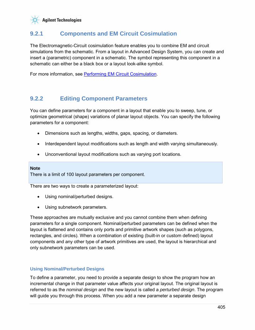
405
9.2.1 Components and EM Circuit Cosimulation
The Electromagnetic-Circuit cosimulation feature enables you to combine EM and circuit simulations from the schematic. From a layout in Advanced Design System, you can create and insert a (parametric) component in a schematic. The symbol representing this component in a schematic can either be a black box or a layout look-alike symbol.
For more information, see Performing EM Circuit Cosimulation.
9.2.2 Editing Component Parameters
You can define parameters for a component in a layout that enable you to sweep, tune, or optimize geometrical (shape) variations of planar layout objects. You can specify the following parameters for a component:
• Dimensions such as lengths, widths, gaps, spacing, or diameters.
• Interdependent layout modifications such as length and width varying simultaneously.
• Unconventional layout modifications such as varying port locations.
Note There is a limit of 100 layout parameters per component.
There are two ways to create a parameterized layout:
• Using nominal/perturbed designs.
• Using subnetwork parameters.
These approaches are mutually exclusive and you cannot combine them when defining parameters for a single component. Nominal/perturbed parameters can be defined when the layout is flattened and contains only ports and primitive artwork shapes (such as polygons, rectangles, and circles). When a combination of existing (built-in or custom defined) layout components and any other type of artwork primitives are used, the layout is hierarchical and only subnetwork parameters can be used.
Using Nominal/Perturbed Designs
To define a parameter, you need to provide a separate design to show the program how an incremental change in that parameter value affects your original layout. The original layout is referred to as the nominal design and the new layout is called a perturbed design. The program will guide you through this process. When you add a new parameter a separate design

Electromagnetic
406
containing a copy of the nominal design is created. You should make your changes in this design by applying perturbations as specified in the Edit/View perturbation dialog. The modified copy is then saved as the perturbed design. You need to define a separate perturbed design for each parameter.
1. Select EM > Component > Parameters to open the Design Parameters dialog box.
2. Type a parameter name in the Name text box.
3. Ensure Nominal/Perturbed is selected in the Type drop-down list.
4. Type a nominal value and select a unit from the drop-down list.
5. Type a perturbed value.
6. Click Add to add the parameter or Edit/View Perturbation to display the Edit/View Perturbation dialog box where you can specify a Linear Stretch, Radial Stretch, or Rotation perturbation for the specified parameter.
The following section describes these values.
Linear Stretch Specifying a linear stretch for a parameter enables you to move a single selected vertex point or a group of selected vertex points linearly using a deltaX, deltaY specification.
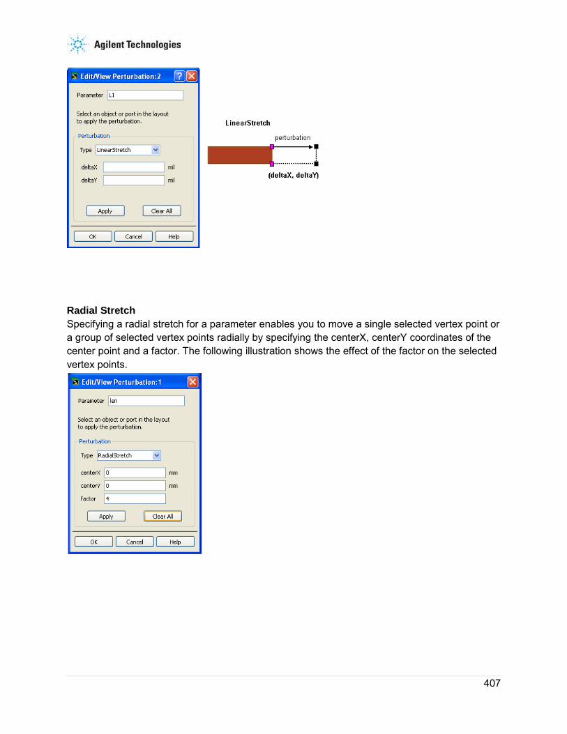
407
Radial Stretch Specifying a radial stretch for a parameter enables you to move a single selected vertex point or a group of selected vertex points radially by specifying the centerX, centerY coordinates of the center point and a factor. The following illustration shows the effect of the factor on the selected vertex points.

Electromagnetic
408
Rotation Specifying a rotation for a parameter enables you to move a single selected vertex point or a group of selected vertex points by rotating over a specified angle around a center point specified by the coordinates centerX and centerY.
9.2.3 Using Existing Components
You can set up a parameterized layout by using a combination of several built-in components. Use the Design Parameters dialog box (EM > Component > Parameters ) to specify subnetwork parameters for the layout component. Once a subnetwork parameter is defined, it can be used to set the parameters values of one or more component instances used in the layout. A parameterized layout can be set up using a combination of several built-in components. You can define a subnetwork for hierarchical components only.

409
Caution Only the top-level design parameters can be used to set the lower-level instance parameters. The use of any other variable is prohibited.
To specify subnetwork parameters for the layout component:
1. Select EM > Component > Parameters to open the Design Parameters dialog box.
2. Type a parameter name in the Name text box.
3. Select Subnetwork in the Type drop-down list.
4. Type a default value and select a unit from the drop-down list.
5. Click Add to add the parameter.
Once a subnetwork parameter is defined, it can be used to set the parameters values of one or more component instances used in the layout. For example, in the following figure, subnetwork parameter L1 is used to set parameter value L of the MLIN instance.
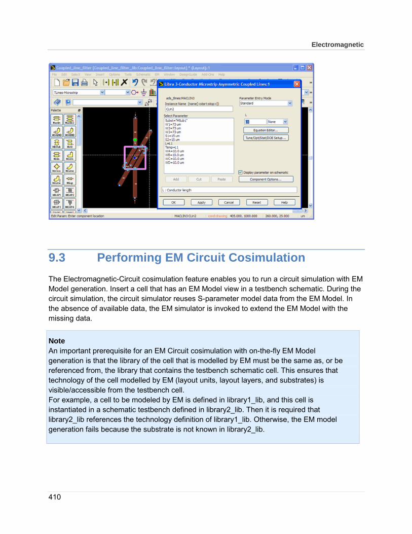
Electromagnetic
410
9.3 Performing EM Circuit Cosimulation The Electromagnetic-Circuit cosimulation feature enables you to run a circuit simulation with EM Model generation. Insert a cell that has an EM Model view in a testbench schematic. During the circuit simulation, the circuit simulator reuses S-parameter model data from the EM Model. In the absence of available data, the EM simulator is invoked to extend the EM Model with the missing data.
Note An important prerequisite for an EM Circuit cosimulation with on-the-fly EM Model generation is that the library of the cell that is modelled by EM must be the same as, or be referenced from, the library that contains the testbench schematic cell. This ensures that technology of the cell modelled by EM (layout units, layout layers, and substrates) is visible/accessible from the testbench cell. For example, a cell to be modeled by EM is defined in library1_lib, and this cell is instantiated in a schematic testbench defined in library2_lib. Then it is required that library2_lib references the technology definition of library1_lib. Otherwise, the EM model generation fails because the substrate is not known in library2_lib.

411
9.3.1 Setting up a Layout
There are two basic ways to create a layout. Use the one that best complements your own design methodology and suits your design needs:
• Layout synchronized from a schematic
• Directly drawn or imported layout
9.3.2 Defining the EM Simulation Setup
Once you have a layout, you need to create an EM Setup view that specifies the EM simulation setup:
1. Specify the substrate
2. Define the ports
3. Set up the simulation options, such as mesh parameters.
4. Specify a frequency plan for the EM model generation
Ports Width
Specifying correct port width is an important factor during EM cosimulation. For example, if you want to connect a strip line of 0.1 mm to a layout design of width 10 mm, you need to create a small polyline of width 0.1 mm.
In this example, you can create a polyline at points where you want to connect another strip line and ports.(Edge ports can also be used in these scenarios).
9.3.3 Defining Component Parameters
You can define component parameters that paramterize the layout. For more information, see Defining Component Parameters.
Electromagnetic
412
9.3.4 Creating an EM Model and Symbol
A symbol is used to represent the component in a schematic. Symbols are stored in Symbol views and must be created before they can be used. For more information on symbols, see Working with Symbols.
An EM Model is used by the circuit simulator to model a component by using the S-parameters generated by an EM simulation. The EM-based S-parameters can be precomputed or you can generate them while running the circuit simulation. An EM Model caches the S-parameters to improve circuit simulation performance. For more information about how to use an EM model, see Using an EM Model.
You can generate an EM model and symbol by selecting EM > Component > Create EM Model and Symbol in the layout window. You can also use the EM Setup window to generate an EM model and symbol. The EM Setup window provides options to customize the model and symbol generation. For more information, see Generating an EM Model and Symbol.
9.3.5 Using Components in a Schematic
The Symbol view of the cell can be inserted into a schematic by typing the name of the component in the component name entry field, or by dragging the component from the ADS Main window in the Schematic window.
9.3.6 Running an EM Circuit Cosimulation
According to the standard simulation hierachy policy, when a cell instance has an EM Model view named "emModel", the circuit view is used for simulation. You can override the view choosen for simulation by selecting the component symbol and click the Choose View for Simulation button. Select the view you want from the Choose View for Simulation window. For more information, see Using an EM Model.
9.3.7 Example
This section provides an exercise illustrating how to set up, perform and view the results of EM Circuit Cosimulation.
Opening an Example Project
Start by opening an ADS Momentum example project into your local directory.
1. From the Main window, select File > Example > Momentum.
2. Select Microwave and select Coupled_line_filter_wrk and click Open.
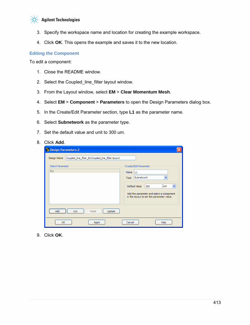
413
3. Specify the workspace name and location for creating the example workspace.
4. Click OK. This opens the example and saves it to the new location.
Editing the Component
To edit a component:
1. Close the README window.
2. Select the Coupled_line_filter layout window.
3. From the Layout window, select EM > Clear Momentum Mesh.
4. Select EM > Component > Parameters to open the Design Parameters dialog box.
5. In the Create/Edit Parameter section, type L1 as the parameter name.
6. Select Subnetwork as the parameter type.
7. Set the default value and unit to 300 um.
8. Click Add.
9. Click OK.

Electromagnetic
414
10. In the Layout window, double-click the component to select it.
11. Select Parameter L in the MLIN column and set Line Length L to L1 in Length.
12. Click OK.
Creating an EM Model
To create an EM model:
1. Choose EM > Simulation Setup to open the EM Setup window.
2. Select Model/Symbol in the left pane of the EM Setup window.
3. Click Create Now.
Adding and Using the Component in a Schematic
To add the parameterized component in schematic:
1. Click New Schematic Window from the ADS Main window to open a new Schematic window.
2. Specify the cell name.
3. Select ads_templates_s_params from the Schematic Design Templates drop-down list.
4. Click OK.
5. Type the cell name and press Enter to place the EM model component.

415
6. Click End Command.
7. Click Insert Wire to connect the symbol with the terminals.
8. Click End Command.
Performing EM Circuit Cosimulation
To perform EM circuit cosimulation:
1. Select the EM Model.
2. Click Choose View for Simulation ( ).
3. Choose EmModel view.
4. Click OK.
5. Click Simulate to perform circuit Cosimulation.
You can now view the results of EM circuit cosimulation in the Data Display window.
9.4 Using the EM Circuit Excitation AEL Addon
Momentum Circuit Excitation allows you to view surface currents and far-field plot of your EM Model with SMDs and any other circuit elements contribution in your schematic. It provides the following features:
• Supports AC/Harmonic balance simulation.
• Supports Parameter sweep and Optimization.

Electromagnetic
416
• Calculates surface currents for an EM models.
• Supports far field view of multiple instances of an EM Model.
Surface currents or fields can be visualized for a passive layout simulated by EM for single or multi-mode port excitations. You can use this AEL addon to run an AC or Harmonic Balance simulation on a schematic that contains an EM Model for the layout and any other circuit elements, such as SMDs. The voltages at all pins of the layout are stored versus frequency. This excitation is then used to compute the surface current distribution and optionally the far field at the EM simulation frequencies. The results can viewed by selecting the 'Extracted Excitation'.
9.4.1 Enabling the EM Circuit Excitation AEL Addon
To enable the EM Circuit Excitation AEL Addon:
1. Select Tools > Manage ADS AEL Addons in the ADS Main window.
2. Select the Enabled check box for EM Circuit Excitation, as shown in the following figure:
3. Click Close.
4. Restart ADS.

417
5. Open a Schematic window and select EM > Circuit Excitation.
Before using this addon, ensure that you have selected either All generated frequencies or User specified frequencies in Output Plan options:
9.4.2 EM Circuit Excitation Flow
To use the EM Circuit Excitation AEL Addon, you need to perform the following steps:
1. Create EM Model views.
2. Create a circuit with AC or Harmonic balance controller.
3. Run the AC/HB simulation.
4. View surface currents.
5. View Far Field.
To use EM Circuit Excitation, perform the following steps:
1. Select EM > Circuit Excitation in the Schematic window. The Circuit Excitation dialog box is displayed.
2. Click Run AC/HB Simulation to start circuit simulation and post processing.
Note
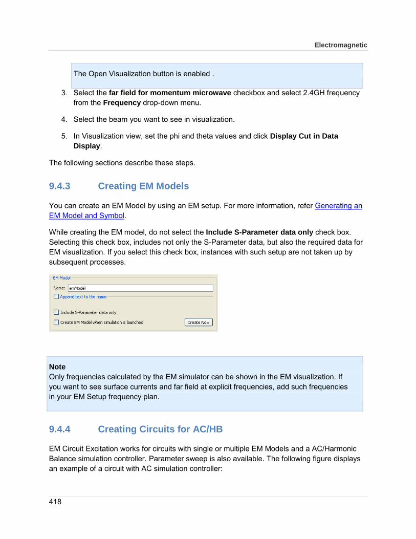
Electromagnetic
418
The Open Visualization button is enabled .
3. Select the far field for momentum microwave checkbox and select 2.4GH frequency from the Frequency drop-down menu.
4. Select the beam you want to see in visualization.
5. In Visualization view, set the phi and theta values and click Display Cut in Data Display.
The following sections describe these steps.
9.4.3 Creating EM Models
You can create an EM Model by using an EM setup. For more information, refer Generating an EM Model and Symbol.
While creating the EM model, do not select the Include S-Parameter data only check box. Selecting this check box, includes not only the S-Parameter data, but also the required data for EM visualization. If you select this check box, instances with such setup are not taken up by subsequent processes.
Note Only frequencies calculated by the EM simulator can be shown in the EM visualization. If you want to see surface currents and far field at explicit frequencies, add such frequencies in your EM Setup frequency plan.
9.4.4 Creating Circuits for AC/HB
EM Circuit Excitation works for circuits with single or multiple EM Models and a AC/Harmonic Balance simulation controller. Parameter sweep is also available. The following figure displays an example of a circuit with AC simulation controller:

419
For creating circuits for AC/HB, choose an EM Model view explicitly for the required instances. Only such instances are available for EM visualization. The excitation voltages for each instance for EM visualization is interpolated or extrapolated based on available frequencies of the AC/Harmonic Balance simulation.
Note Currently AC and Harmonic balance simulation are supported.

Electromagnetic
420
9.4.5 Running AC/HB Simulation
1. Select EM > Circuit Excitation in the schematic window. The Circuit Excitation dialog box is displayed, as shown in the following figure:
2. Click Run AC/HB Simulation to start circuit simulation and post processing.
Note If you have included an optimization controller in your circuit and want to run optimization, select the Optimization check box. However, if you have selected Enable Optimization Cockpit in the optimization controller, optimization flow might not work properly from this tool. To avoid this issue, you can disable this option. In the schematic, double-click Optimization controller, select the Parameters tab, and remove selection from Enable Optimization Cockpit.
3. A message box stating that Compute excitation is all finished is displayed.
9.4.6 Viewing Results
To view surface currents:
1. Select an instance from the Instance drop-down list.
2. Click Open Visualization.
3. In the EM Visualization window, select the Solution Setup tab.

421
4. Select Extracted Excitation.
Note It is recommended to reset the maximum amplitude for plots after selecting Extracted Excitation because it has largely different maximum amplitude than Single Mode Excitation. To reset maximum amplitude for each plots type, click Options > Restore System Max/Min.
5. Select a state and frequency for displaying the results.
Note If you swept parameters by parameter sweep, each of these simulation becomes a State.
To view far fields:
1. Select an instance in the Instance drop-down list.
2. Select the Far Field (uW mode only) check box and select a frequency.
3. Click Open Visualization to view results, as shown in the following figure:

Electromagnetic
422

423
Chapter 10 – EMPro and ADS Integration Agilent EEsof provides a way to combine the capabilities of EMPro and ADS by using a common database. The following features are supported in EMPro:
• Import EMPro results and design data in ADS.
• Perform EM circuit co-simulation from the ADS Schematic window.
• Improve usability of the existing EMPro components by adding EM ports in ADS.
• EMPro and ADS Integration Process
• Saving EMPro Designs in a Library
• Adding an EMPro Library in ADS
• Adding EMPro Components in ADS Layout
• Using EMPro Components in ADS Schematic
o Adding EMPro Components to Schematic
o Exporting EMPro Simulation Results as emModel
• Exporting ADS Layouts to EMPro
• EMPro ADS Integration FAQs
• Application- SI Analysis of Interconnects using EMPro-ADS Interoperability
• Example- Using the EMPro Connector Design in ADS
10.1 EMPro and ADS Integration Process EMPro 2012.09 provides an enhanced process for integrating EMPro and ADS. EMPro designs are stored in a cell, which contains multiple views. You can use these views in ADS layout and schematic.

Electromagnetic
424
EMPro and ADS Integration
EMPro and ADS Integration Process The following flowchart depicts the ADS and EMPro integration process:
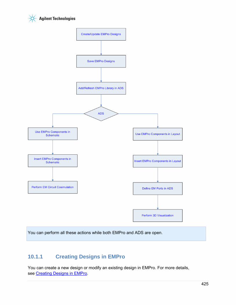
425
You can perform all these actions while both EMPro and ADS are open.
10.1.1 Creating Designs in EMPro
You can create a new design or modify an existing design in EMPro. For more details, see Creating Designs in EMPro.

Electromagnetic
426
10.1.2 Saving EMPro Designs in a Library
From EMPro 2012 release onwards, EMPro designs are saved as cells in a library. You can import this library in ADS. For more details, see Saving EMPro Designs in a Library.
10.1.3 Adding an EMPro Library in ADS
To use EMPro designs in ADS, add the EMPro design library in an ADS workspace. For more details, see Adding an EMPro Library in ADS.
10.1.4 Using EMPro Components in ADS Layout
From an EMPro library, you can use the footprint or layout view in the ADS layout. For more details, see Adding EMPro Components in ADS Layout.
10.1.5 Using EMPro Components in ADS Schematic
From an EMPro library, you can use the symbol or lookalike view in the ADS schematic. For more details, see Using EMPro Components in ADS Schematic.
10.2 Saving EMPro Designs in a Library From EMPro 2012 release onwards, your EMPro designs are saved in a library. After you have saved the design, a cell with multiple views is created and stored in a library. You can import this library in ADS.
Designs created with EMPro 2012 that are saved as cells and views in a library cannot be opened with older releases. However, from within EMPro 2012, you have the option to save the design in the legacy format (.ep). Designs created with previous releases can be opened in EMPro 2012 and can be saved in the new library cell/view format (recommended) or in the legacy format (.ep). When saved in the new library cell/view format, the legacy files on your system remain unchanged.

427
While saving an EMPro project, you can specify the following project types:
• EMPro OpenAccess projects: Enables you to save EMPro projects in a library, unless you explicitly specify a project name that ends with .ep. If the chosen destination is not within a library, a new library is created with the same name as the project.
• EMPro Legacy projects: Enables you to save EMPro projects in the legacy (.ep) format.
• All OpenAccess cells: Enables you to save projects in a library, unless you explicitly type a new project name that ends with .ep. If the chosen destination is not within a library, a new library is created with the same name as the project.
• All files: Displays all files. It enables you to save a project in a library, unless you explicitly type a new project name that ends with .ep. If the chosen destination is not a library, a new library will be created with the same name as the project.
10.2.1 Saving Designs in a Library
To save a design in a library:
1. Select File > Save Project As to open the Save Project As dialog box.
2. Choose the required location for saving your project.
3. Click Create New OpenAccess Library ( ). A new library is created in the Save Project As dialog box.

Electromagnetic
428
4. Specify a name for your library, as shown in the following figure:
5. Double-click the new library.
6. Type a name for your project or accept the default name.
7. Accept the default project type, EMPro OpenAccess projects.
8. Click Save.
If new cells are added to the EMPro library, select View > Refresh (F5) to refresh the library view in the ADS Main window. If a particular cell is changed from within EMPro, you need to insert a new instance in the ADS design to capture the changes. For example, if the number of ports changed, you need to add the updated cell in ADS.
10.2.2 Saving Existing 3D Components in a Library
You can also save components that were created using older versions of EMPro in a library. These projects, which were created in the .ep format, can be easily saved in the new format. You need to open an existing project and save it as a library. While opening a project, you can select one of the following project types:

429
• All EMPro Projects (OA,.ep): Displays all EMPro projects that are created in the OpenAccess (OA) and .ep format.
• EMPro OpenAccess projects: Displays only OpenAccess cells that are EMPro projects.
• EMPro Legacy projects: Displays only EMPro projects that are created in the legacy format (.ep).
• All files: Displays all files.
To open an older version project:
1. Choose File > Open Existing Projects to display the Open Existing Project dialog box.
2. Select the required project type.
3. Select the existing project you want to open.
4. Click Open.
After opening the project, you can save it in the new library format. Perform the following steps:
1. Open a legacy EMPro design.

Electromagnetic
430
2. Select File > Save Project As to open the Save Project As dialog box.
3. Choose the required location for saving your project.
4. Type a name for your project.
5. Select EMPro OpenAccess projects as the project type.
6. Click Save.
10.2.3 Creating Designs in EMPro
To create an EMPro design, perform the following tasks:
1. Create a Geometry.
2. Assign Materials to components.
3. Set Mesh Priority.
4. Define Ports.
5. Specify Simulation Setup.
Step 1: Create a Geometry
To create new objects or modify existing objects, use the Create Geometry toolbar.
Example: Creating a Parametrized Geometry To create a parametrized geometry:
1. Click Extrude in the Geometry window.
2. Select the object you want to create.
3. Click the Extrude tab and enter the Extrude Distance.
4. Click Done. The geometry view displays the objects that you have created.
5. Click the Specify Orientation tab to specify the origin of the model.
6. Click and select the Origin tool.
7. Click the Edit Cross Section tab.
8. Click the Extrude tab.
9. Type package_length in the Extrude Distance text box. The edit box will turn red as soon as the focus is shifted away from the edit box or when you press Enter. This

431
indicates that the value is interpreted as an expression containing an unknown parameter.
10. Click Done. The geometry view will not show the top box as the modeling sequence contains the unknown parameter package_height.
11. Click Parameters ( ) to open the Parameters window.
12. Click to add a new parameter.
13. Add the parameter package_height and set Formula to 1 mm.
Assign Materials to Components
After creating a parametrized component, assign materials to the component, as follows:
1. Click Parts and choose Create New > Assembly. Drag the two generated objects into the Assembly.
2. Choose Materials > Select from Default Material Library to open the Material Library window.
3. Double-click Copper.
4. Click Add.
5. Drag the material Copper and drop it on the geometry.
Few materials are not supported by 3D components due to limitations in the FEM simulator.
Set Mesh Priority
To set the mesh priority of a component:
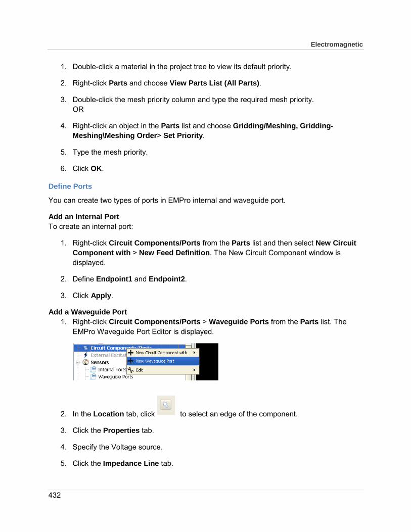
Electromagnetic
432
1. Double-click a material in the project tree to view its default priority.
2. Right-click Parts and choose View Parts List (All Parts).
3. Double-click the mesh priority column and type the required mesh priority. OR
4. Right-click an object in the Parts list and choose Gridding/Meshing, Gridding- Meshing\Meshing Order> Set Priority.
5. Type the mesh priority.
6. Click OK.
Define Ports
You can create two types of ports in EMPro internal and waveguide port.
Add an Internal Port To create an internal port:
1. Right-click Circuit Components/Ports from the Parts list and then select New Circuit Component with > New Feed Definition. The New Circuit Component window is displayed.
2. Define Endpoint1 and Endpoint2.
3. Click Apply.
Add a Waveguide Port 1. Right-click Circuit Components/Ports > Waveguide Ports from the Parts list. The
EMPro Waveguide Port Editor is displayed.
2. In the Location tab, click to select an edge of the component.
3. Click the Properties tab.
4. Specify the Voltage source.
5. Click the Impedance Line tab.
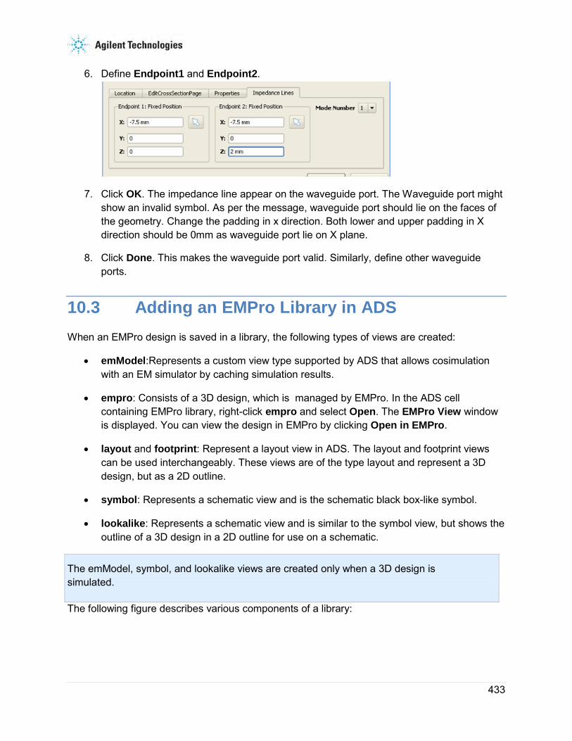
433
6. Define Endpoint1 and Endpoint2.
7. Click OK. The impedance line appear on the waveguide port. The Waveguide port might show an invalid symbol. As per the message, waveguide port should lie on the faces of the geometry. Change the padding in x direction. Both lower and upper padding in X direction should be 0mm as waveguide port lie on X plane.
8. Click Done. This makes the waveguide port valid. Similarly, define other waveguide ports.
10.3 Adding an EMPro Library in ADS When an EMPro design is saved in a library, the following types of views are created:
• emModel:Represents a custom view type supported by ADS that allows cosimulation with an EM simulator by caching simulation results.
• empro: Consists of a 3D design, which is managed by EMPro. In the ADS cell containing EMPro library, right-click empro and select Open. The EMPro View window is displayed. You can view the design in EMPro by clicking Open in EMPro.
• layout and footprint: Represent a layout view in ADS. The layout and footprint views can be used interchangeably. These views are of the type layout and represent a 3D design, but as a 2D outline.
• symbol: Represents a schematic view and is the schematic black box-like symbol.
• lookalike: Represents a schematic view and is similar to the symbol view, but shows the outline of a 3D design in a 2D outline for use on a schematic.
The emModel, symbol, and lookalike views are created only when a 3D design is simulated.
The following figure describes various components of a library:

Electromagnetic
434
10.3.1 Adding an EMPro library in ADS
In ADS, a library includes multiple cells each containing a view that is used for a particular tool operating on the design. For example, symbol views are used in ADS Schematic, while a layout view can be manipulated by ADS Layout. Together, these views form a cell. EMPro, similarly, allows you to manage a design stored in the database. For example, consider an SMA connector that is created in EMPro. After adding this connector in ADS, the cell can include an emModel or layout view. You can insert the emModel view directly in an ADS schematic and use for circuit/EM cosimulation. Similarly, you can insert a layout view on an ADS layout design for performing 3D simulations in ADS.
To add an EMPro library in ADS:
1. Select File > Manage Libraries from the ADS Main window. The Manage Libraries window is displayed.

435
2. Click Add Library.
3. Click Yes to close the message box. The Add Library dialog box is displayed.
4. Specify the path of your EMPro library. You can also click Browse to access the required library.
5. Select the required library mode from the Mode drop-down list.
6. Click OK. The EMPro design is imported as a cell with multiple views in the ADS Main window.
10.3.2 Using Libraries, Cells, and Views in ADS
After saving your EMPro designs in a library, you can import the library in an ADS workspace. A workspace is used to store and organize the design work in Library:Cell:View hierarchical architecture. EMPro components are added to a cell in the workspace. A cell contains various types of views that represent different aspects of the component, such as layout, schematic, or symbol.
Library:Cell:View hierarchy

Electromagnetic
436
ADS Library
In ADS, a library is a subdirectory that includes cells. Libraries are used by specifying the subdirectory in a library definition file, such as lib.defs. This file defines name of the library and the mode of operation (Read Only, Non-Shared, or Shared). Files within the library itself define the technology (layers, resolution, and layout units) to be used by Views created in that library. All types of designs are contained in libraries.
The process information such as layer definitions, units, and substrates are defined in the technology of a library. You can create multiple libraries within a complete design hierarchy. A library resides physically in the workspace directory.
Key Features of an ADS Library The following are the key features of a library in ADS:
• Each Library has a unique name and path, specified in a library definition file. A library itself does not specify its name. The name must be specified correctly in a lib.defs file.)
Note Two libraries with the same name cannot be open at the same time.
• Associated with a Technology that defines physical layers, and units. The technology can be a native one created for a library, or it can be referenced to another library.
• Contains zero (0) or more Cells.
• Loaded/unloaded independently or collectively loaded through a lib.defs file.
• Defines the technology (layers, resolution, layout units). All views in a library use the same technology.
• Can be opened in following three modes:
o Read-only Mode: In this mode, you cannot modify or commit changes to the library cells and the cell views. You need to use the Only Save As option. will work.
o Shared Mode: In this mode, you can jointly modify and/or commit changes to the library cells and cell views with others that might have access to the same ADS library location.
o Non-Shared Mode: In this mode, only you can commit any changes to the library’s cells and cell views when library is open.
• Can reside physically anywhere in the system, with the following conventions:

437
o All ADS components are inside Read-only ADS libraries which are stored with the product.
o Normal end-user libraries are usually stored in a workspace. You can add a library from another workspace into the current workspace.
Note In ADS 2011, Workspaces are not included inside another workspace. Instead, a lib.defs file from another workspace can be added to the current workspace using DesignKits > Manage Libraries... from the ADS Main Window.
Cell
A Cell is a container of Views. Each Cell:
• Must have a unique name in the library, although cells with the same name may exist in another library.
• Contains zero or more views.
• May have multiple views of the same type.
• May have a component definition, edited by choosing File > Design Parameters... while editing one of its views.
View
A View is a subdirectory in a cell that stores design information such as schematic, symbol, or layout. Views may also store an EM simulation setup or an EM Model. Each view is a container that stores a file or a database object. It is a specific representation of a cell. All views in a given library use the same technology.
Each view:
• is associated with a Cell.
• must have a unique name in the Cell.
Note Schematic, Layout, and Symbol Views should generally be named as schematic, layout, and symbol unless you are using polymorphism.
• Has a type (schematic, layout, symbol, EM Setup, EM Model).

Electromagnetic
438
10.4 Adding EMPro Components in ADS Layout
An EMPro library consists of a footprint and layout view that can be placed on an ADS Layout. After adding EMPro components in a layout, you can customize parameters and define EM ports on these components in ADS.
Perform the following steps to use EMPro components in ADS:
1. Save your EMPro designs in a library. For more information, see Saving EMPro Designs in a Library.
2. Import the EMPro library in ADS. For more information, see Adding an EMPro Library in ADS.
3. Place EMPro components in the ADS Layout window.
4. Defining EM Ports on EMPro components.
5. Assigning Pins to EMPro Ports.
6. Perform simulation using EMPro components.
This section provides information about how to add EMPro components in ADS layout, assign pins, and perform co-simulation with an ADS board.
10.4.1 Inserting EMPro Components in ADS Layout
Before using EMPro components in ADS Layout, the technology database of empro_standard_layers library must be referenced by the workspace library. The artwork (footprint) of 3D components and their port-pins are drawn on the empro_3dc_artwork and the empro_3dc_pins layers, respectively. These layers are saved in the empro_standard_layers library. The layer on which a 3D component pin is drawn together with the net determines its logical connectivity.
This is needed only if you want to create ports on the EMPro components in layout.
Referencing the EMPro Standard Layer Library
To link the empro_standard_layers library to your design in ADS:
1. Select Options > Technology > Technology Setup.

439
2. Click the Referenced Technology tab.
3. Click Add Referenced Library.
4. Add empro_standard_layers, as shown in the following figure:
5. Click OK.
Adding EMPro Components from the ADS Main Window
To insert an EMPro component in ADS layout:
1. Open a Layout window in ADS.
2. From the ADS Main window, select the layout or footprint view in the cell imported from EMPro.
3. Drag and drop the selected component in the ADS layout window. The Properties dialog box is displayed.
4. Modify the component properties as per your requirements in the Properties dialog box.
5. Click OK. An EMPro component is included in the ADS layout. You can now rotate and position the component in your layout design.

Electromagnetic
440
Adding EMPro Components using the Component Library Window
Alternatively, you can also insert a component by using the Component Library window. Perform the following steps:
1. Click in the ADS Layout window. The Component Library window is displayed.
2. Access the library imported from EMPro in Workspace Libraries.
3. Double-click the required component from the Component column. The Choose View window is displayed.
4. Select footprint or layout from the Component column.
5. Drag and drop the component on the Layout window.
10.4.2 Customizing Component Parameters in ADS
You can customize the following EMPro component parameters in ADS
Parameter Description CustomComponentLayer Layer in the substrate corresponding to Z=0 in
the 3D Component. CustomComponentOnTop Alignment of Z=0 in the 3D Component with
top/bottom of the layer. CustomComponentRotateX Rotates the component around the X axis. CustomComponentRotateY Rotates the component around the Y axis. CustomComponentMirrorZ Mirrors the component about the XY plane,
boolean that triggers the projection f(z)=-z. CustomComponentOffsetZ Adds an additional translation in Z direction to
the component, z distance specified by user. minFreq Minimum frequency of interest for the project. maxFreq Maximum frequency of interest for the project.
10.4.3 Defining EM Ports on EMPro Components
If you have defined ports in the EMPro design, the instance pins are visible in layout (diamond shape) corresponding to the connection points of the ports defined in EMPro. You can also add pins in the top layout, connected to the instance pins.

441
When a pin is recognized as a 3D pin, it displays text 3D.
To add pins:
1. Select Insert > Pin in the ADS Layout window.
2. Place the pins at the required location of the ports imported from EMPro, as shown in the following figure:
If two 3D pins map on the same 2D coordinates on footprint, the 2D projection of one pin is displaced with respect to other to select each pin. However, the 3D locations are not changed.
10.4.4 Waveguide Port
A waveguide port definition on an EMPro component can be used to create either a calibrated port or non-calibrated port when using this component in ADS layout. By default, the waveguide port definition will lead to a calibrated port. To do this, reference the empro_standard_layers technology to your design (see Adding EMPro Components in ADS Layout), add pins to the + and – instance pins of the EMPro component, and associate both pins to the TML port in the EM Setup window.
The location of the + and – instance pins correspond to the location of the end points of the impedance lines of the waveguide port. The waveguide port setup parameters as defined in EMPro will be used as the port parameters in the simulation driven from layout.
In case the calibrated port is not be located on the boundary of the simulation domain (e.g. because of the presence of other metal shapes), it will be automatically translated into a circuit component port.
You can manually force the waveguide port definition to be translated to a non-calibrated port by marking the port to be of calibration type None in the EM Setup window.
10.4.5 Circuit Component Port
A circuit component port definition on an EMPro component can only be used to create a non-calibrated port definition in ADS layout. To do this,reference the empro_standard_layers technology to your design (see Adding EMPro Components in ADS Layout), add pins to the +

Electromagnetic
442
and – instance pins of the EMPro component and associate both pins to a non-calibrated port in the EM Setup window. The location of the + and – instance pins corresponds to the location of the end points of circuit component port.
ADS allows a geometrical connection between ADS and EMPro components. You need to assign EM pins to an EMPro component only when you need to measure power of the component.
10.4.6 Assigning Pins to EMPro Ports
To assign layout pins to EMPro ports:
1. Select EM > Simulation Setup to open the EM Setup window.
2. Select Ports in the left pane of the EM Setup window.
3. Select an EMPro pin in Layout Pins.
4. Drag the pin from Layout Pins and drop it on the or terminal of the required port in S-parameter Ports.
443
5. A message box is displayed if your target pin is already used by other ports.
6. Click Delete Ports and Continue in the message box.
Note You can drag and drop multiple layout pins and connect with a S-parameter port.
After assigning layout pins, launch FEM from layout and simulate your design. The EM Setup window determines simulation parameters.
For more information, see Defining Ports in EM Simulations.
10.4.7 Performing 3D Visualization
You must complete the simulation process to view data for your EMPro design imported in ADS. If you have already simulated a design, start the Visualization feature directly to view the existing data. In the ADS layout, select EM > Post-Processing > Visualization to open the Agilent FEM Visualization window. You can also open this window by clicking Visualization (
) in the EM toolbar.
To visualize FEM simulations:
1. Choose EM > Simulation Setup to open the EM Setup window.
2. Select FEM in the EM Setup window.
3. Specify the required settings in the EM Setup window for a layout, substrate, port, frequency plan, output plan, options, resources and model or symbol.
4. Click Simulate in the EM Setup window to simulate your design.
5. Select EM > Post-Processing > Visualization to preview your design.
For more information, see Viewing 3D Simulations.
10.5 Using EMPro Components in ADS Schematic • Adding EMPro Components to Schematic
• Exporting EMPro Simulation Results as emModel
Electromagnetic
444
10.5.1 Adding EMPro Components to Schematic
Using EMPro designs, you can perform EM circuit cosimulation in the ADS Schematic window. An EMPro component is represented by a symbol or lookalike in ADS Schematic. You can also perform cosimulation by using the S-parameters generated by an EMPro simulation. For more information, see Exporting EMPro Simulation Results as emModel.
Perform the following steps to use EMPro components in ADS Schematic:
1. Save your EMPro designs in a library. For more information, see Saving EMPro Designs in a Library.
2. Import the EMPro library in ADS. For more information, see Adding an EMPro Library in ADS.
3. Place EMPro components in the ADS Schematic window.
4. Perform EM circuit cosimulation using EMPro components.
This section provides information about how to add EMPro components in ADS Schematic and perform EM circuit cosimulation with an ADS board.
Inserting EMPro Components in Schematic
You can insert the symbol components imported from an EMPro library in ADS Schematic. To insert a component, type the name of the component in the component name field or drag the component from the ADS Main window. The EMPro ports become schematic pins that can be connected to other components.
Adding EMPro Components from the ADS Main Window To add an EMPro component in the ADS Schematic window:
1. Open a Schematic window in ADS.
2. From the ADS Main window, select symbol or lookalike from the cell imported from EMPro.

445
3. Drag and drop the selected component in the Schematic window, as shown in the following figure:
Adding EMPro Components using the Component Library Window Alternatively, you can also insert a component by using the Component Library window. Perform the following steps:
1. Click . The Component Library window is displayed.
2. Access the library imported from EMPro in Workspace Libraries.
3. Double-click the required component from the Component column. The Choose View window is displayed.
4. Select symbol or lookalike from the Component column.
5. Drag and drop the selected component on the Schematic window.
Performing EM Circuit Cosimulation
After inserting a symbol or lookalike component in the ADS Schematic window, you can perform EM circuit cosimulation. The EM circuit cosimulation feature enables you to combine EM and circuit simulations from the schematic.
To perform the EM circuit cosimulation using EMPro components in ADS Schematic:

Electromagnetic
446
1. Start ADS and open a workspace.
2. Place the symbol or lookalike component in the Schematic window.
3. Connect the imported symbol with other components.
4. Select the component and click Choose View for Simulation .
5. Select the emModel view for simulation.
6. Click OK.
7. Click Simulate .
See Also EM Circuit Cosimulation
10.5.2 Exporting EMPro Simulation Results as emModel
You can export EMPro simulation results as an ADS-compatible cell. The export process creates a cell with two views, emModel and symbol. You can use these cells in the ADS Schematic window. In ADS, a circuit simulator uses the S-parameters results of an EMPro simulation. If you have performed simulations from within EMPro, the resulting S-parameter models are available as emModels for use in the circuit simulation flow. The emModel names refer to the simulation id, such as 000001 and 000002.
Perform the following steps to export EMPro simulation results:
1. Create an emModel and symbol in EMPro.
2. Import the EMPro cell in ADS.
3. Place the cell in the ADS Schematic window.
4. Perform simulation using the imported cell.
This section describes the process of creating an emmodel and symbol, importing EMPro cell, and performing simulation using S-parameters results.
Creating emModel in EMPro
To create an EM model component in EMPro:
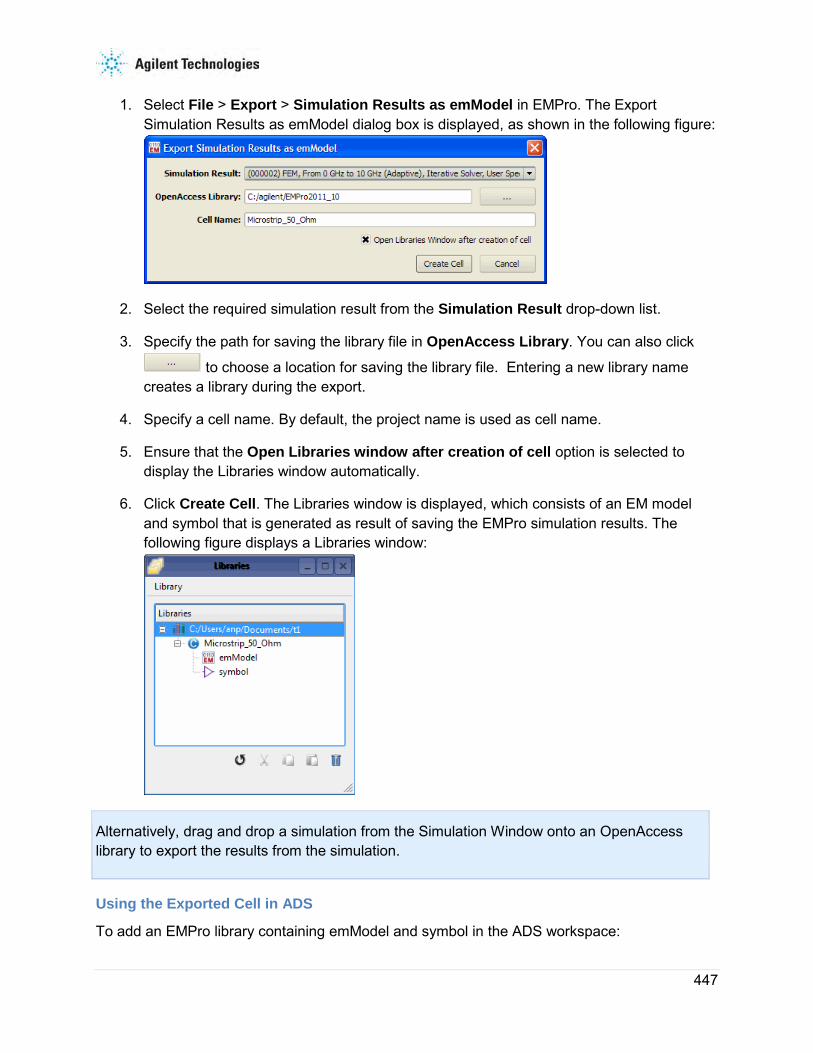
447
1. Select File > Export > Simulation Results as emModel in EMPro. The Export Simulation Results as emModel dialog box is displayed, as shown in the following figure:
2. Select the required simulation result from the Simulation Result drop-down list.
3. Specify the path for saving the library file in OpenAccess Library. You can also click
to choose a location for saving the library file. Entering a new library name creates a library during the export.
4. Specify a cell name. By default, the project name is used as cell name.
5. Ensure that the Open Libraries window after creation of cell option is selected to display the Libraries window automatically.
6. Click Create Cell. The Libraries window is displayed, which consists of an EM model and symbol that is generated as result of saving the EMPro simulation results. The following figure displays a Libraries window:
Alternatively, drag and drop a simulation from the Simulation Window onto an OpenAccess library to export the results from the simulation.
Using the Exported Cell in ADS
To add an EMPro library containing emModel and symbol in the ADS workspace:
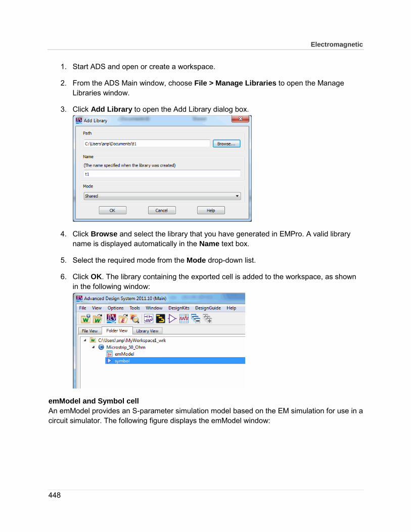
Electromagnetic
448
1. Start ADS and open or create a workspace.
2. From the ADS Main window, choose File > Manage Libraries to open the Manage Libraries window.
3. Click Add Library to open the Add Library dialog box.
4. Click Browse and select the library that you have generated in EMPro. A valid library name is displayed automatically in the Name text box.
5. Select the required mode from the Mode drop-down list.
6. Click OK. The library containing the exported cell is added to the workspace, as shown in the following window:
emModel and Symbol cell An emModel provides an S-parameter simulation model based on the EM simulation for use in a circuit simulator. The following figure displays the emModel window:

449
The following figure displays an example of a symbol imported from EMPro:

Electromagnetic
450
You can place the cell in a Schematic design in several ways, such as using the Place Component command or by typing the cell name in the inserted component history field. Alternatively, drag and drop the cell from the libraries view on the Schematic window.
Performing a Simulation in ADS Schematic with the EMPro Exported Cell To perform the circuit simulation and using the EMPro simulation results:
1. Start ADS and open or create a workspace.
2. Place the emModel or symbol in the Schematic window.
3. Connect the imported symbol with the terminals of other components.
4. Select the symbol and click Choose View for Simulation .
5. Choose the emModel view for simulation.
6. Click OK.
7. Click Simulate .
10.6 Exporting ADS Layouts to EMPro You can transfer an ADS layout to a new EMPro project by using the following options:
• Using the Launch EMPro and import this design Option: You can use the Launch EMPro and import this design option in ADS 2011 to export designs from ADS and import the designs in EMPro. This operation requires you to set the variable ADS_EMPROHOME in the file $HOME/hpeesof/config/hpeesof.cfg to the directory containing the EMPro executable. If this variable is not set, the Export to EMPro dialog

451
box is displayed automatically. In this dialog box, choose the EMPro installation directory and click OK.
• Using the Create a self-contained import script Option: You can use the Create a self-contained import script option in ADS 2011 to specify a location for saving a self-contained Python script. To complete the conversion, import and execute this script in an empty EMPro design. You can use this process when ADS and EMPro are not installed on the same machine.
To transfer ADS layouts:
1. Set the $HOME/hpeesof/config/hpeesof.cfg variable ADS_EMPROHOME to the directory containing the EMPro executable file. You can use the hpeesof.cfg variable ADS_EMPRO_OPTIONS for specifying additional command-line arguments for EMPro.
2. Select EM > Simulation Setup to display the EM Setup window.
3. Select FEM in the EM Setup window, as shown in the following figure:
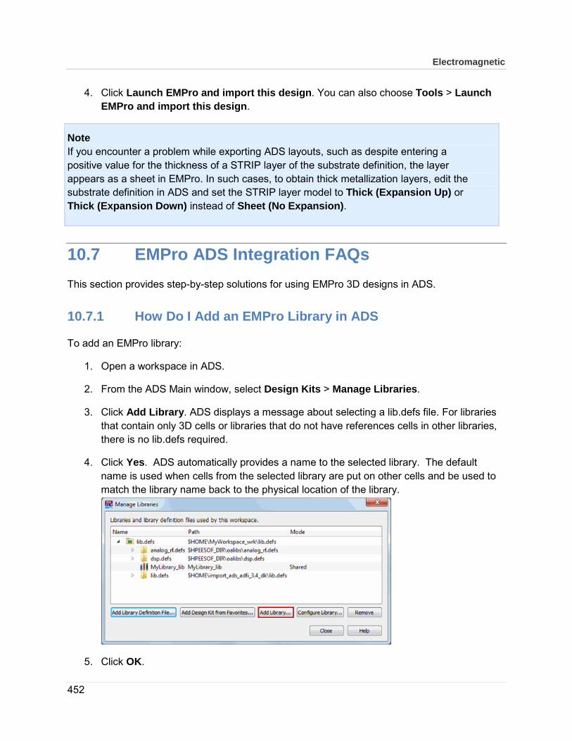
Electromagnetic
452
4. Click Launch EMPro and import this design. You can also choose Tools > Launch EMPro and import this design.
Note If you encounter a problem while exporting ADS layouts, such as despite entering a positive value for the thickness of a STRIP layer of the substrate definition, the layer appears as a sheet in EMPro. In such cases, to obtain thick metallization layers, edit the substrate definition in ADS and set the STRIP layer model to Thick (Expansion Up) or Thick (Expansion Down) instead of Sheet (No Expansion).
10.7 EMPro ADS Integration FAQs This section provides step-by-step solutions for using EMPro 3D designs in ADS.
10.7.1 How Do I Add an EMPro Library in ADS
To add an EMPro library:
1. Open a workspace in ADS.
2. From the ADS Main window, select Design Kits > Manage Libraries.
3. Click Add Library. ADS displays a message about selecting a lib.defs file. For libraries that contain only 3D cells or libraries that do not have references cells in other libraries, there is no lib.defs required.
4. Click Yes. ADS automatically provides a name to the selected library. The default name is used when cells from the selected library are put on other cells and be used to match the library name back to the physical location of the library.
5. Click OK.
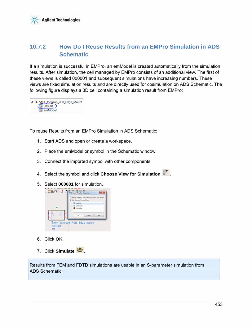
453
10.7.2 How Do I Reuse Results from an EMPro Simulation in ADS Schematic
If a simulation is successful in EMPro, an emModel is created automatically from the simulation results. After simulation, the cell managed by EMPro consists of an additional view. The first of these views is called 000001 and subsequent simulations have increasing numbers. These views are fixed simulation results and are directly used for cosimulation on ADS Schematic. The following figure displays a 3D cell containing a simulation result from EMPro:
To reuse Results from an EMPro Simulation in ADS Schematic:
1. Start ADS and open or create a workspace.
2. Place the emModel or symbol in the Schematic window.
3. Connect the imported symbol with other components.
4. Select the symbol and click Choose View for Simulation .
5. Select 000001 for simulation.
6. Click OK.
7. Click Simulate .
Results from FEM and FDTD simulations are usable in an S-parameter simulation from ADS Schematic.

Electromagnetic
454
10.7.3 How Do I Sweep an EMPro 3D Design using FEM in ADS
A complete EMPro 3D design is encapsulated in a cell. Cosimulation is supported through the emModel and empro views.
To sweep an EMPro 3D Design using FEM in ADS:
1. Drag and drop the symbol or lookalike view on ADS Schematic. Optionally, verify if the emModel view is selected for simulation.
2. Select the symbol and click Choose View for Simulation .
3. Select emModel. The default hierarchy policy is to use the emModel. The following figure displays parameter sweeping a 3D design using ADS Schematic:
10.7.4 How Do I Simulate an ADS Board with an EMPro 3D Design in ADS Schematic
You can simulate a board created in ADS together with a full 3D design created in EMPro by using ADS Schematic as driver. Perform the following steps:
1. Simulate the board using ADS Layout and create an emModel from the simulation.
2. Open an ADS Schematic window and place the generated emModel on the schematic.
3. Add the library with the 3D design to your ADS workspace.
4. Place the emModel components of the 3D design on the schematic and connect all the pins to create your required schematic.
5. Click Simulate . If the emModel databases are already populated with simulation results, the circuit simulator reuses the existing results. If the emModel database is empty, then proper cosimulation is performed.
Cosimulation with a 3D design from ADS Schematic is supported only if the 3D design is

455
set up for simulation with FEM. If another simulator is desired, simulate from within EMPro and reuse the existing results.
10.7.5 How Do I Simulate an ADS Board with an EMPro 3D Design in ADS Layout
You can simulate a board created in ADS together with a full 3D design created in EMPro using ADS Layout as driver. Perform the following steps:
1. Open the board in ADS Layout.
2. Add the library containing the 3D design to your ADS workspace.
3. From the library, drag and drop the footprint view of the cell containing the 3D design on to your ADS Layout window containing the board.
4. Set the simulation options by using the EM Setup window.
5. Select the FEM simulator to perform the simulation.
6. Click Simulate .
You can perform ADS layout simulation of EMPro 3D designs only by using the FEM simulator (the Momentum simulator does not support layout simulation).
10.7.6 How Do I Simulate a Board Created in ADS Layout together with a EMPro 3D Design using EMPro as Driver
To simulate an EMPro design in ADS layout:
1. Open the board in ADS layout.
2. Set up the board for EM simulation.
3. Use the EM Setup window to perform the necessary setup steps. You can modify all simulation setup options later in EMPro. Therefore, you can use either the ADS EM Setup window or the tools from within EMPro to setup ports, simulation boundaries, sweeps, and other parameters. In general, it is more efficient to perform port setup from within ADS.The layout is now ready to be exported to EMPro.

Electromagnetic
456
4. Click Launch EMPro and import this design. Alternatively, a stand-alone script can be generated that you can run from within EMPro to reconstruct the board, including any setup made, in EMPro.
10.7.7 How Do I Move the Height of the Instantiation of a 3D Component
The height where a 3D component is instantiated is controlled by two parameters: CustomComponentLayer and CustomComponentOnTop. The parameter CustomComponentLayer is a layer being used to determine the Z location of the 3D component. It implies the layer has to be mapped into the substrate. The second parameter CustomComponentOnTop allows for thick layers to select between the bottom or the top of the layer to be used for the effective Z location.
10.7.8 How Do I Set the Origin of a 3D Component
The effective location of a 3D design in an ADS workspace is also determined by the location of the original 3D design. The absolute origin (0,0,0) of the 3D designs corresponds to the anchor point used in simulation driven from ADS layout to determine the final position of the 3D design in a combined board and 3D connector analysis. EMPro renders the absolute origin when the bounding box visualization of geometry is turned on.
The following figure shows origin of a 3D cell displayed in EMPro:
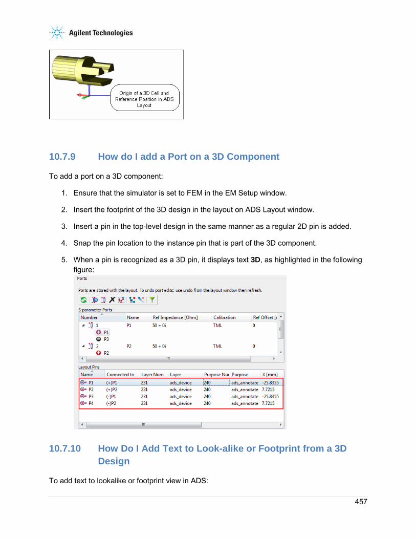
457
10.7.9 How do I add a Port on a 3D Component
To add a port on a 3D component:
1. Ensure that the simulator is set to FEM in the EM Setup window.
2. Insert the footprint of the 3D design in the layout on ADS Layout window.
3. Insert a pin in the top-level design in the same manner as a regular 2D pin is added.
4. Snap the pin location to the instance pin that is part of the 3D component.
5. When a pin is recognized as a 3D pin, it displays text 3D, as highlighted in the following figure:
10.7.10 How Do I Add Text to Look-alike or Footprint from a 3D Design
To add text to lookalike or footprint view in ADS:
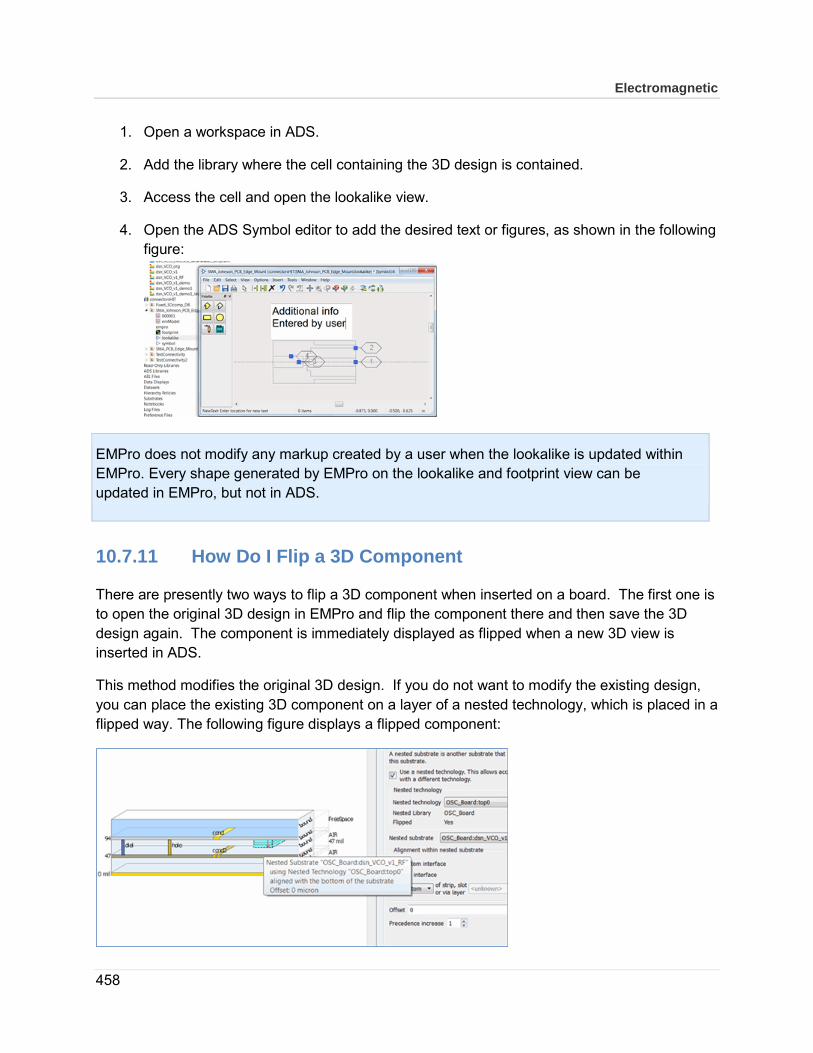
Electromagnetic
458
1. Open a workspace in ADS.
2. Add the library where the cell containing the 3D design is contained.
3. Access the cell and open the lookalike view.
4. Open the ADS Symbol editor to add the desired text or figures, as shown in the following figure:
EMPro does not modify any markup created by a user when the lookalike is updated within EMPro. Every shape generated by EMPro on the lookalike and footprint view can be updated in EMPro, but not in ADS.
10.7.11 How Do I Flip a 3D Component
There are presently two ways to flip a 3D component when inserted on a board. The first one is to open the original 3D design in EMPro and flip the component there and then save the 3D design again. The component is immediately displayed as flipped when a new 3D view is inserted in ADS.
This method modifies the original 3D design. If you do not want to modify the existing design, you can place the existing 3D component on a layer of a nested technology, which is placed in a flipped way. The following figure displays a flipped component:

459
10.7.12 How Do I Change the Layer of the Footprint View
To change the layer of a footprint view in ADS:
1. Open the footprint view in ADS.
2. Click Select or Select All to select all the components present on the view.
3. Select Edit > Properties. The Properties dialog box is displayed.
4. Select the required layer.
If the technology of the library does not have any layers, the layer selection will be empty. In that case, first add a layer to the technology of the library.
After changing layers, if the design is updated and the footprint view needs to be updated, EMPro will not change the layer position, but update the footprint but not the layer. EMPro verifies whether all EMPro-generated layouts are moved consistently to another layer. If all layers are not moved, EMPro will move all layout to the original layer.
3D cells can be saved in any library, so it is often beneficial to save them in a library that already contains the technology definition that can be used in ADS. When EMPro creates a library, the technology does not contain any layers by default.
10.7.13 How Do I Scale or Offset a Lookalike Symbol
By default, lookalike symbols are generated using a set of rather simple heuristics to determine the final size. To customize the scale value of a lookalike view:
1. Open the view in ADS layout.

Electromagnetic
460
2. Click Select or Select All to select all the components present on the view.
3. Select Edit > Scale/Oversize \ Scale.
4. Specify the required scale factor. After editing the scale factor, you still need to select a center of scaling.
Similarly, you can offset by selecting Edit > Move or Move Relative.
If a lookalike view is scaled or offset, EMPro does not change the scaling and offset. Therefore, if the original lookalike is 3 inches wide on ADS Schematic, any update of the lookalike from within EMPro keeps the outline of the design within the lookalike view within 3 inches. Similarly, if the lookalike view was shifted 2 inches up, any updates to the lookalike view is generated with the same offset value.
10.7.14 How Do I Use a 3D Component Created in an Earlier Version of EMPro
To use a 3D component created in previous versions of EMPro:
1. Open the original 3D design (typically stored in an .ep directory or zep file) in EMPro 2012.
2. Click Save As.
3. Select the OpenAccess library where you want to store the 3D design. Now, you can use the 3D design as a 3D component.

461
10.8 Example- Using the EMPro Connector Design in ADS
This section describes how to use the EMPro connector design, SMA Johnson Edge Mount, in ADS. The Connector design used in this example consists of:
• Parameter definition for permittivity dielectric coax, eps_coax.
• Design has two component ports:
o Port 1 on the side that connects to the ADS board.
o Port 2 on the coax side, which is a component port.
Perform the following tasks:
• Open the SMA_Johnson_Edge_Mount Project and modify the design.
• Save the Connector Design in an EMPro Library.
• Import the EMPro library in ADS.
• Use EMPro Connector in Schematic.
• Use EMPro Connector in ADS Layout
10.8.1 Open the SMA Johnson Edge Mount Project in EMPro
To display SMA Johnson Edge Mount project in EMPro:
1. Open the Libraries window in EMPro 2012.09.
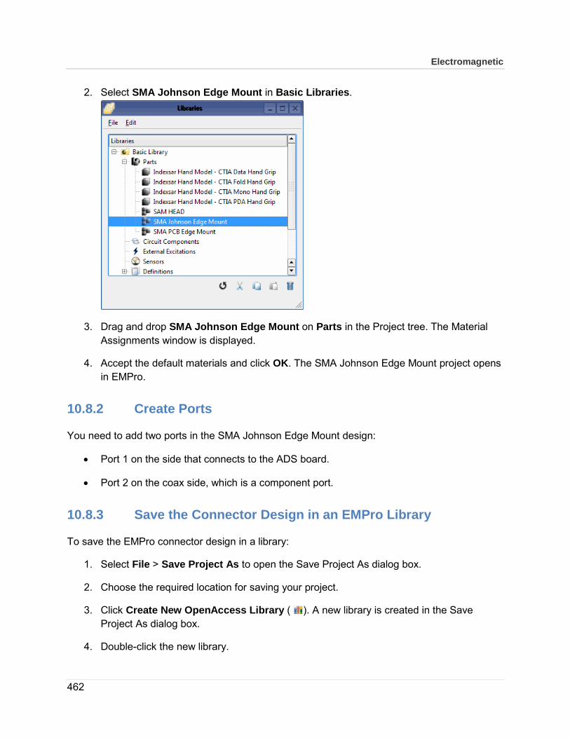
Electromagnetic
462
2. Select SMA Johnson Edge Mount in Basic Libraries.
3. Drag and drop SMA Johnson Edge Mount on Parts in the Project tree. The Material Assignments window is displayed.
4. Accept the default materials and click OK. The SMA Johnson Edge Mount project opens in EMPro.
10.8.2 Create Ports
You need to add two ports in the SMA Johnson Edge Mount design:
• Port 1 on the side that connects to the ADS board.
• Port 2 on the coax side, which is a component port.
10.8.3 Save the Connector Design in an EMPro Library
To save the EMPro connector design in a library:
1. Select File > Save Project As to open the Save Project As dialog box.
2. Choose the required location for saving your project.
3. Click Create New OpenAccess Library ( ). A new library is created in the Save Project As dialog box.
4. Double-click the new library.
463
5. Specify empro_comp_lib as name for your library.
6. Accept the default name for your project, SMA_Johnson_PCB_Edge_Mount.
7. Accept the default project type, EMPro OpenAccess projects.
8. Click Save. This saves the EMPro design in the new format, ready for use in ADS.
10.8.4 Import the EMPro library in ADS
To open EMPro library containing the connector design in ADS:
1. Select File > Manage Libraries from the ADS Main window. The Manage Libraries window is displayed.
2. Click Add Library. A message box is displayed.
3. Click Yes to close the message box. The Add Library dialog box is displayed.
4. Click Browse to access the required design.
5. Select empro_comp_lib.
6. Click OK. The EMPro design is imported as a cell with multiple views in the ADS Main window as shown in the following figure:
10.8.5 Open Design in ADS
To integrate EMPro components with an ADS design, open the following workspace:
ADS Install directory>\Examples\FEM\EMPro_ADS_handson_wrk.7zads
To open the EMPro_ADS_handson_wrk.7zads workspace in ADS:
1. Select File > Open > Example. The Select an Archive File dialog box is displayed.
2. Double-click the FEM folder.
3. Select EMPro_ADS_handson_wrk.7zads.
4. Click Open. The Unarchive Wizard is displayed.
5. Provide a destination path for unarchiving your example workspace.

Electromagnetic
464
6. Click Next.
7. Select EMPro_ADS_handson_wrk.
8. Click Finish.
10.8.6 Use EMPro Connector in Schematic
To add an EMPro component in the ADS Schematic window:
1. Open the simulate_schematic window from the EMPro_ADS_handson_wrk.7zads workspace.
2. From the ADS Main window, select symbol from the cell, SMA_Johnson_PCB_Edge_Mount, imported from EMPro.
3. Drag and drop the symbol component in the Schematic window.
4. Connect the imported symbol with other components by adding connectors, mind polarity and port numbering, as shown in the following figure:
5. Select the symbol and click Choose View for Simulation.
6. Select the emModel view for simulation.
7. Click OK.
8. Click Simulate. It triggers the following sequence of actions:
• Retrieve existing EM model for the board.
• FEM simulation for connector, eps is equal to 2.

465
• FEM simulation for connector, eps is equal to 4.
• Perform Circuit simulation.
10.8.7 Use EMPro Connector in ADS Layout
To use connectors in a layout:
1. Open the layout design from the EMPro_ADS_handson_wrk.7zads workspace:
2. From the ADS Main window, select footprint from the cell imported from EMPro.
3. Drag and drop the footprint component in the ADS layout window. The Properties dialog box is displayed.
4. Insert the first connector, and select pc2 as the layer to match the z-location.
5. Accept the default values and click OK. The EMPro connector is added to the ADS layout.
6. Insert the second connector, rotate and position, and select pc2 as the layer to match the z-location.
7. Add four pins on layer ads_device: drawing, connected to the instance pins of the connectors
8. Place the pins at the required location of the ports imported from EMPro, as shown in the following figure:
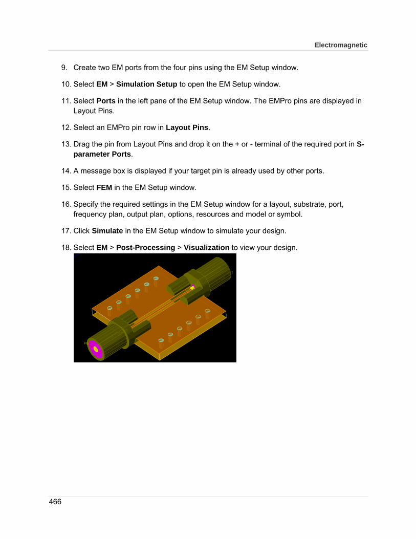
Electromagnetic
466
9. Create two EM ports from the four pins using the EM Setup window.
10. Select EM > Simulation Setup to open the EM Setup window.
11. Select Ports in the left pane of the EM Setup window. The EMPro pins are displayed in Layout Pins.
12. Select an EMPro pin row in Layout Pins.
13. Drag the pin from Layout Pins and drop it on the + or - terminal of the required port in S-parameter Ports.
14. A message box is displayed if your target pin is already used by other ports.
15. Select FEM in the EM Setup window.
16. Specify the required settings in the EM Setup window for a layout, substrate, port, frequency plan, output plan, options, resources and model or symbol.
17. Click Simulate in the EM Setup window to simulate your design.
18. Select EM > Post-Processing > Visualization to view your design.

467