electronics research laboratory - eecs at uc berkeley · electronics research laboratory universiy...
TRANSCRIPT

Iterated Timing Analysis and SPLICE1
bY
Rewe A Saleh
June 1983
Electronics Research Laboratory
Universiy of California
Berkeley, California 84720

Abettact
SPLICE1 is a mixed-mode simulation program for large-scale integrated
circuits. I t performs concurrent electrical and logic simulation using event-
driven selective-trace techniques. The electrical analysis uses a new algo-
rithm, called Iterated Timing Analysis (ITA), which performs accurate electri-
cal waveform analysis much faster than SPICEZ. The logic analysis features a
new MOS-oriented state model and a fanout dependent delay model, and han-
dles bidirectional transfer gates in a consistent manner.
This report describes the new algorithms and the details of the imple-
mentation in SPWCEl.6. Program performance characteristics and a
number of simulation results are also included.


Acknowledgements
I would like to express my appreciation to my research advisor Prof. A.
Richard Newton for his patience, encouragement and guidance throughout
course of this work. I would also like to thank Prof. Don 0. Pederson and
Prof. Albert0 Sangiovanni-Vincentelli for their support.
I wish to thank everyone in the CAD group at Berkeley but a few people
dcscrvc spccial mcntion. In particular, I would likc to thank Jim Klcckncr for
the many long hours of help generating examples, fixing bugs and engaging
in useful discussions. I am also grateful to Jacob White for the discussions on
the theoretical aspects of the work.
I wish to acknowledge the assistance of Graeme Boyle, Steve Potter and Jack
Hurt and convey my appreciation to Ian Getreu and John Crawford at Tek-
tronix in Beaverton, Oregon. I would also like to send a special thanks to
Mike Caughey and the ICCAD group at MITEL Ccrp. in Ottawa, Canada for their
encouragement.
Finally, I wish to thank my wife, Lynn, and my family members for their con-
tinuing support.
This work was supported in part by NSERC (Natural Science and Engineering
Research Council) of Canada, the Hewlett-Packard Company, Digital Equip-
ment Corporation and Tektronix Corporation.


CHAPTER 1: INTRODUCTION ................................................................. 1
CHAPIlER 2 Iterated Timing Analysis ................................................... 4
2.1 Introduction ......................................................................................... 4
2.2 The Simulation Problem ...................................................................... 4
2.3 Motivation for a New Simulation Approach .......................................... 5
2.4 Relaxation-based Electrical Simulation ............................................... 10
2.5 The ITA Algorithm ................................................................................ 11
2.5.1 The Gauss-Seidel Iteration Method ................................................ 11 2.5.2 A Non-linear Gauss-Seidel Iterative Approach ............................... 13
2.5.3 The SOR-Newton Iteration .............................................................. 15
2.5.4 Convergence of the SOR-Newton Iteration ..................................... 16
2.6 Implementation in SPLlCE ................................................................... 17
2.6.1 Program Flow ................................................................................. 18
2.6.2 Details of Node Processing ............................................................. 18
2.6.3 Element Models .............................................................................. 19
2.7 ITA Simulation Results ......................................................................... 20
2.8 Optimizations in the Present Implementation .................................... 21
Enbancements tn the Logic Analysis .................................. 23 cXAPTEX 3:
3.1 Introduction ......................................................................................... 23
3.2 The State Model ................................................................................... 24
3.2.1 A MOS-oriented Logic Model ........................................................... 24
3.2.2 State Model Definition .................................................................... 25
3.2.3 Using the State Model .................................................................... 27
3.3 The Delay Model ................................................................................... 27
1

i
3.3.1 Factors Affecting Switching Delay ................................................. 27
3.3.2 Delay Model for Simple Gates ........................................................ 28
3.3.3 Delay Model for Multi-output Elements .......................................... 29
3.3.4 Delay Models for Transfer Gates .................................................... 30
3.3.5 Delay to an Unknown Value ............................................................ 32
3.4 Spike h-andling ..................................................................................... 32
3.5 Transfer Gate Modeling Issues ............................................................. 35
3.5.1 Bidirectional Transfer Gates .......................................................... 35
3.5.2 Unknoxns at Cntc Inputs ............................................................... 36
3.5.3 Node Decay .................................................................................... 38
3.6 Logic Simulation Implementation Details ............................................ 39
3.6.1 General Program Flow ................................................................... 39
3.6.2 Node Processing Details ................................................................. 39
3.7 Switch-level Simulation ....................................................................... 40
C H A P E R 4: Egamples and Results ....................................................... 42
4.1 Program Performance Statistics ......................................................... 43
4.2 Profile Statistics .................................................................................. 45
4.3 Factors Atfecting Execution Time in Electrical Simulation ................. 46
4.3.1 CPU-time vs . MRT ........................................................................... 46 4.3.2 CPU-time vs . MIPU’DVSCH ................................................................. 47
4.3.3 Effect of Floating Capacitors ......................................................... 48
4.3.4 CPU-time vs . SOR ........................................................................... 49
4.4 SPICE2 vs . SPICE1.6 ............................................................................. 49
4.5 NMOS OpAmp Example ......................................................................... 50
CHAPTF, R 5: CONCLUSIONS .................................................................. 52

APFTNDIX I: SPLIcE1.6 User's Guide
APPENDM 11: spLICE1.6 Data Structures
APPENDIXIII: SPUCE1.6 Electrical Model Eqyations


1
m i z e d m o d e simulation program for large digital MOS
1. INTRODUCIION
SPLICE1 is a
integrated circuits (IC). It performs time-domain transient analysis which
tends to be the most time-consuming and memory-intensive task in simula-
tion today. The enhancements made to the program are described in this
report. The starting point for this work was SPLICE1.3[ 11 . This early version
of SPLICE1 included 4-state logic simulation, simple timing analysis and a
SPICE-like circuit simulation capability[ 1,2] . While this version provided a degree of functionality, it suffered from
modeling and accuracy problems intrinsic to the algorithms used in the pro-
gram. Specifically, the 4-state logic model was not sufficient to perform an
accurate true-value logic simulation of general MOS circuits containing
transfer gates and wired connections (Le.. more than one gate controlling
the state of a node). The simple timing analysis algorithm had inherent
accuracy limitations and stability problems and had some difficulty handling
circuits containing floating elements and tight feedback loops. These, and
other issues, are examined in detail elsewherel31 and will be elaborated
further in later sections.
The latest version, SPLICE1.6, overcomes these problems by using
state-of-the-art algorithms in place of previous ones.
The electrical analysis is performed using a new technique called
Iterated riming Analysis (ITA) which can be derived from simple timing
analysis[4,5] . In this approach the non-linear differential circuit equations
are solved using a converged relaxation iteration instead of the direct matrix
. solution approach used in standard circuit simulators[6] . I t is as accurate

2
as SPICEZ, assuming identical device models, and has guaranteed conver-
gence and stability properties. Due to the selective trace feature in SPLlCE1,
the execution time is up to two orders of magnitude faster than SPICE2 for
comparable waveform accuracy. Another key feature of the ITA method is its
ability to perform a transient analysis of complex analog circuits, as will be
shown later. Iterated Timing Analysis has shown so much promise that
efforts are being directed to generalize it as a standard technique for accu-
rate electrical simulation. Therefore, a matrix-oriented simulation capabil-
ity is no longcr available in SPLTCEl.
The logic analysis capabilities have also been extended to include the
notion of multiple strengths or impedance levels [3] as is available in most
modern MOS-oriented logic simulators[?, 8,9,10] . While other simulators
usually limit the number of strengths to three, there is no practical limit in
SPLICE1.6, which allows up to Z I 6 - 1 levels. More than three strengths are
often required to model the interaction between transfer gates of differing
geometry[3] . The processing of the gates and nodes proceeds in a manner
similar to the electrical analysis. In fact, the logic analysis may be thought
of as a relaxation-based method in which the elements are represented by
simple logic models rather than complex analytical equations. This concept,
together with the idea of multiple impedance levels, allows for a more con-
sistent signal representation and signal conversion in the mixed-mode
environment. Clearly, there is a correspondence between an electrical vol-
tage and the logic levels. With the notion of strengths, there is now a natural
correspondence between the electrical output conductance of an element
and the logic output strength of the element.

3
SPLICE1 can also be used to perform a switch-level simulation[9, 101 to
verify circuit functionality at the transistor level. I t handles CMOS, NMOS and
PMOS circuits in both static and dynamic configurations. SPLICE1.6
currently performs unit-delay simulation of switch-level circuits.
Although SPLICE1 originally included a table look-up scheme to speed up
MOS model evaluation[4,5] it was subsequently dropped from the program.
Research on optimal tablc models and structurcs is continuing in an
independent eflort 1111 and this featgre FF.~ be reinstated in a later version.
Therefore, this report doss not edd:-es% the EX? of table-driven MUS models.
The remainder of this repnrt is di--i&L is to foiir chapters. In Chap. 2,
the ITA algorithm is dei.5t-?d in_ dc:tzil. The enhancements made to the logic
analysis ?.re p r e s e c t ~ d irz Ck;. 1,. chq . 4 pro-ides scrne insight into the new
algorithms through the us? GI* e x m q d e s . Finally, in Chapter 5, the general
conclusion: are st3C,e?. -*.<th s,??c?k 13eA.iox Gf future directions.
4
2. Iterated Timing Analysis
2.1. Introduction
A new form of electrical analysis, called Iterated Timing Analysis (ITA),
is described in this chapter. The motivation for this work is presented using
SPLICE1.3 as an example of Non-iterated Timing Analysis (NTP,). A simple
mathematical treatment of the ITA method is presented here although a
complete mathematical analysis of relaxation-based mekhods, presented in a
rigorous and unified framework, may be found in reference[ 121 . The details
of the implementation in SPLICE1.6 are also included in this chapter.
2.2. The Simulation b b l e m
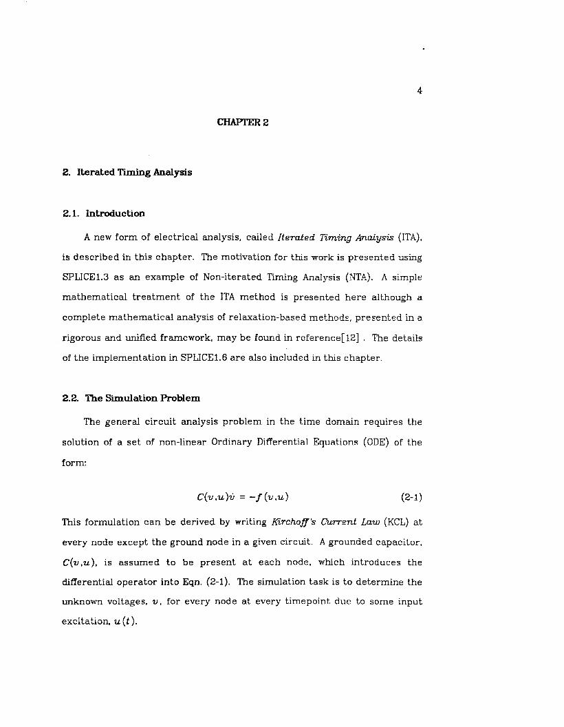
The general circuit analysis problem in the time domain requires the
solution of a set of non-linear Ordinary Differential Equations (ODE) of the
form:
This formulation can be derived by writing Kirchog’s Current Law (KCL) at
every node except the ground node in a given circuit. A grounded capacitor,
C(v,u), is assumed to be present at each node, which introduces the
differential operator into Eqn. (2-1). The simulation task is to determine the
unknown voltages, v , for every node at every timepoint due t o some input
excitation, u ( t ).

5
The technique used in SPICE2 to solve Eqn. (2-1) is to first convert the
set differential equations into a set of algebraic, difference equations using a
stiffly-stable integration formula[6] . Then the non-linear difference equa-
tions are converted to a set of linear equations of the form:
using a damped Newton-Raphson linearization process. G is the Jacobian
matrix (or the small-signal conductance matrix), V is the unknown voltage
vector and I is the known excitation vector. Finally, (2-2) is solved using a
direct matrix approach to produce the solution vector, V.
2.3. Motivation for a New Simulation Approach
General-purpose sirnulaliori programs such as SPICE2 [6] and ASTAP[ 131
have been used extensively to perform accurate circuit analysis for over 10
years. These simulators use direct methods (using sparse matrix tech-
niques) to solve the set of circuit equations. Unfortunately, the cost of using
these simulators in terms of computer CPU-time and memory requirements
becomes prohibitive as the size of the circuit increases. The fundamental
problem is illustrated in Fig. 2.1. While the time required to formulate the
equations grows linearly with circuit size, the solution time is proportional to
IVk where N is the number of circuit nodes and k ranges from 1.1 to 1.5.
This is one reason why the direct approach becomes increasingly expensive
as the circuit size increases.
Timing simulation was introduced in the mid-seventies to reduce CPU-
time at the expense of some accuracy. A new breed of simulators emerged
at that time. all tailored to handle the transient analysis of large digital cir-

10'
1 oa
1 oz CPU
TIME (SI
10
1
Figure 2.1 : Equation Formulation and Solution times
for standard circuit simulation
I I 1
/
/
, I I I
. I I
,
I I I I I
10 1 oe 1 os 1 o4 NUMBER OF CIRCUIT EQUATIONS
cuits[5,4,1, 14,151 . These classical timing analysis programs used iterative
techniques [IS] to solve the set of circuit equations rather than the direct
matrix solution approach of the previous generation. A grounded capacitor
was required at every node to gaurantee convergence of the method. How-
ever, to reduce the execution time, none of these programs carried the
iteration to convergence and in fact each node equation was only solved once
at each timepoint.
Large digital ciruits typically displays a 10-20 Z latency characteristic.
That is, only 10-20 % of the nodes in the circuit are active at any given time.
Conceptually, there is temporal sparsity (latency in a waveform over a time
period) and spatial sparsity (latency in the network at a given point in
timer171 . Since these iteration methods involve the solution of each equa-
tion separately, this latency aspect could be exploited to further improve
performance.
Using these techniques, two orders of magnitude of speed improvement
was obtained. Accuracy was maintained in these simulators by choosing a
small fixed timestep for the entire analysis. This timestep was either con-
stant for all circuits [5] or chosen based on the smallest time constant in the
circuit[4] . Later timing simulators adjusted the timestep during the
analysis dynamically to limit the voltage change over a timestep to a value
specified by the user[l] . Simple timing analysis also relied heavily on the
fact that the accumulated error becomes zero once a node reaches either of
the two supply voltages.
While offering a substantial savings in CPU-time and memory usage,
these programs suffer from a number of problems which has limited their
use. Circuits containing global feedback loops, such as the ring oscillator of

7
Fig 2.2(a), introduce timing and voltage errors into the simulation. Fig 2.2(b)
illustrates these errors as generated by SPLICE1.3 compared to the solution
produced by SPICE2. The SPLICE1.3 program not only produces a timing
error (phase error) but incorrectly predicts the number of cycles in a given
time period (frequency error) and the height of the peaks (amplitude error).
These errors are all due to the single iteration performed at each
timepoint. To undcrstnnd the origin of thc errors, consider the example of a
simple NMOS inverter of Fig. 2.3(a) and examine the processing sequence in
NTA:
The first step is to convert each non-linear device to its corresponding
companion model. This is done in Fig. 2.3(b). These equivalent models
are based on the terminal voltages of each device. The conductance is
obtained from the slope of the non-linear I-V characteristic at the
operating point and the current is obtained from the y-axis intercept as
shown in Fig. 2.3(c). The value of the voltage a t Node C is calculated
using this equivalent circuit of Fig. 2.3(b). Assume that initially
VB”-’=OV and VCn-’=5.0v, where Vgn-l means the voltage at node B at
time tnw1 and VCn-l has a similar definition.
(2 ) Let VBn=l.Ov. Then the change in the voltage at node C is calculated
using VB’” and VCn-l. Therefore, the linear equivalent model is the same
as it was at tn-l but the equivalent model of the driver changes. Since
load offers less charging current than it really shouid (Le., VC is
incorrect) and the driver is able to sink more current due to a larger
V,, the node voltage change AVc” is too optimistic.
(3) When V’n+1=2.0v , again VCn+l=f (Vcn, VbR+I) and A@!+’ is also optimis-
tic by the same argument given above.

Figure 2.2(a) : NMOS Ring Oscillator Circuit
50 100
t i m e fns)
V
150 n
Figure 2 . 2 ( b ) SPICE2/SPLICE1.3 Comparison
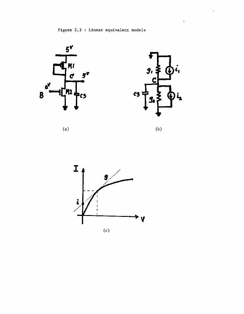
Figure 2.3 : Linear equivalent models

8
Hence, in a SPLlCE1.3 simulation, the output of the inverter will rise and
fall much earlier and faster than the SPICE2 simulation of the same circuit.
This error is propagated and intensified in the ring oscillator circuit, result-
ing in all three errors cited above. I t should be noted that if the timestep of
the simulation is reduced and the accuracy tolerances are tight, the NTA out-
put will be indistinguishable from SPICE2 output for this example.
Anothcr shortcoming of NTA is that it has somc difiiculty dealing with
circuits containing floating elements, such as capacitors and transfer gates.
These elements introduce strong bilateral coupiing between two nodes in the
circuit. Since only one iteration is used, the solution obtained using NTA is
inconsistent. That is, the h a 1 node voltage values depend on the order that
the nodes are processed. Consider, for example, the 2-input NMOS nand cir-
cuit of Fig. 2.3(d). I t contains a "floating" transistor, namely M2. The
sequence of processing in the NTA method would be as follows :
Assume that initially VX~-~=OZI, Vyn-l=5.O2/ and Vjyn-l=OU
At t,,, Vwn=l.Ov and Node X is processed using the initial conditions
lrx"-l and Vp-l given above to produce @.
Next, Node Y is processed using Vyn-' and Vxn to generate Vp.
Then, time is advanced by one unit and steps (2) to (4) are repeated.
This process continues until Node Y makes its transition to the opposite
rail voltage.
There are two problems with this method:
the change in node Y should immediately affect node X but it is not
reflected a t node X until the next time point.

Figure 2.3 (d) : 2-input NMOS NAND circuit
VDD
Figur’e 2 . 4 : Boot-strapped Inverter

9
if the processing started with node Y instead of node X, slightly different
results would be obtained.
The same effect is observed when processing capacitors where one node
is not ccnnected to ground (Le., a floating capacitor). An example of a cir-
cuit with such a capacitor is the boot-strapped inverter of Fig 2.4. The accu-
racy of NTA depends on the timestep and the ratio of the floating capacitor
to the grounded capncit.or. In thc boot-strapped invcrtcr, thc value of C’,,
is usually large compared to the grounded capacitors and this tends to
reduce the accuracy of the solution produced by NTA.
Therefore, it is clear that NTA will produce inaccurate results when
there are floating elements in the circuit. Reducing the timestep to an
appropriate value will improve the accuracy. If the timestep is not small
enough, these elements may cause the simulator to exhibit instability. As
will be seen later in this section, the ITA approach overcomes all of these
problems.
By far the most compromising aspect of the NTA approach is that it may
occasionally produce the wrong answer! Circuit designers are willing to use a
program which gives them the correct answer or no answer (usually due to
non-convergence), but are unable to deal with a program that occasionally
produces the wrong answer. In fact, the NTA method always produce some
answer and this is really the downfall of the method.
For all of the reasons given above, timing analysis has not been widely
accepted as viable form of electrical simulation, although it has been used
successfully in constrained IC design methodologies such as standard cell or
gate array. What is really required is a simulation technique which provides
both accuracy and speed.

10
2.4. Relaxation+ased Electrical Simulation
A number of new techniques have been developed in an efiort to reduce
the simulation time while maintaining waveform accuracy comparable to
SPICE2. These include table-driven model evaluation [ 111 , microcode tailor-
ing on a minicomputer [18] and the use of vector-oriented computers such
as the CRAY-1[19] . Although these techniques have been successful, they
providc, at most, an ordcr of magnitudc spccd improvcmcnt ovcr SPICEZ.
Two methods are currently being investigated which use a converged
relaxation iteration to solve the set of circuit equations. Both approaches
have been implemented and preliminary results indicate that up to two ord-
ers of magnitude of speed improvement may be obtained for large digital cir-
cuits. One method, called Waveform ReLazation[20] , decomposes the sys-
tem of equations into several dynamic subsystems each of which is analyzed
for the entire simulation period. The process is then repeated until all the
waveforms converge to an exact solution. The relaxation is performed at the
differential equation level. This method has been implemented in program
RELAX.[ZO,Zl]
The second method, called Iterated Eming Analysis (ITA) [22,23] . In
this method, the relaxation is performed at the non-linear equation level.
That is, the set of non-lineur circuit equations are iterated to convergence
using a Gauss-Seidel or Gauss-Jacobi method. This is also an exact method.
Some aspects of this method which make it attractive are as follows:
it has guaranteed convergence and stability properties
it allows circuit latency to be exploited easily
it can be implemented using the concepts developed for logic simulation
11
since the logic and electrical analysis operate the same way, a con-
sistent mixed-mode simulation is possible
The algorithm has been implemented in SPLICE1.6 and the implementa-
tion details and results obtained are presented in this chapter folloeng a
simple mathematical treatment of the method.
2.5. The ITA Algorithm
2.5.1. The Gauss-Seidel Iteration Method
A system of simultaneous linear equations can be solved using a variety
of techniques, namely:
1. Direct Methods a. Matrix Inversion b. Gaussian Elimination c. LU decomposition
2. Iterative Methods a. Gauss-Jacobi b. Gauss-Siedel c. SOR-Newton d. Newton-SOR
In circuit simulation, the solution t o Eqn. (2-2) is required. The circuit con-
ductance matrix, G, is usually large but sparse, typically having 3 elements
per row. Matrix inversion is not a suitable method because it usually con-
verts a sparse matrix into a dense one. Sparse matrix techniques can be
used to solve the equations using method l(a) or l(b) but this is a time-
consuming task, as evidenced by Fig. 2.1.
The iterative methods [ 161 are well-suited to cases where the matrix is
sparse and, in fact, a solution may be obtained faster than a direct method in
some cases. Two classical iteration methods exist: the Gauss-Jacobi (G-J)

12
method and the Gauss-Seidel (G-S) method. The Gauss-Jacobi method (also
referred to in the literature as simultaneous displacement) proposes the fol-
lowing approach:
v(O) = initial guess voltage vector me0 repeat
for (i = 1 t o N ) t r
i m + m + l
j until Ivp+',vimI<c for d l i, i.e., convergence
Kotice that every equation uses the previous iteration values for all unk-
nown voltages to obtain a new solution vector. The Gauss-Seidel method (also
referred to as successive displacement) suggests the following modification
to Gauss-Jacobi:
v(O) = initial guess voltage vector m+O repeat
for (i = 1 to N ) f
r n t m + 1 1 until I V ~ + ~ - - ~ ~ , ~ I S E for dl i. i.e., convergence
Notice that each equation uses the latest values of voltage wherever pos-
sible.
The only difference in the two methods is whether the previous voltages
are always used or the latest values are applied immediately. The conver-
gence rate is linear in both cases but the speed of convergence is quite
different. In general, the Gauss-Seidel iteration converges faster than

13
Gauss-Jacobi [16] although examples can be constructed where this is not
true.
Both methods also require the strict diagonal dominance condition for
guaranteed convergence:
This inequality states that each diagonal term of the matrix be greater than
the sum of all the off-diagonal terms in the same row.
A n acceleration scheme is available to speed up convergence by intro-
ducing an acceleration parameter, w. as follows.
where vi is an intermediate value generated using Eqn. (2-4). The effect of w
is usually dramatic but it can only be obtained empirically and usually varies
from technology to technology. For standard Gauss-Seidel, o = 1.
2.5.2. A Non-Linear GaussSeidel Iterative Approach
Relaxation methods, as described in the previous section, can also be
applied successfully at the non-linear equation level. The total number of
iterations may be reduced by using a property of the non-linear iteration.
"he reason for this will be made clear in Sec. 2.5.4.
The following is a description of how this is done is SPLICE1.6. Starting
with equation (2-l), the f i s t step is to convert the differential equations into
difference equations using a stiffly-stable integration formula. SPLICE1.6
uses a Backward-Euler formulation[24] . Then the f i s t equation is linearized
using the Newton-Raphson (N-R) method and iterated to convergence to solve

14
for one unknown voltage. This constitutes the inner N-R loop. The same pro-
cess is applied to the next equation and all subsequent equations, in turn,
until the last equation is processed. This outer G-S loop is now iterated to
convergence to produce the solution.
To further illustrate the method, consider the solution method applied
to one node in a typical circuit. Fig 2.5(a) shows three non-linear devices
connccted to Nodc 4 which itsclf has a capacitor conncctcd to ground. We
begin by writing KCL for Node 4
4 C Ij = r4-r1-r2-r3 = o j = l
This can be rewritten in the form of Eqn. (2-1) :
c4p4 = I l ( vl, v4) + IZ( VZ, 1/41 f Id v3, v4)
Using the Backward-Euler formula for I,, we obtain
(2-7)
(2-9) dF’4 c 4 r4 = e,-= dt +v4(n)-c(n-1) )
where h is the integration step size, V4cn) means the voltage value for Node 4
at time tn and V&-q refers to the solution obtained for Node 4 at time tn-l.
Therefore, Eqn. (2-6) can now b e written as a difference equation,
Since Eqn. (2-10) has the form:
f (Vl* v2, v3, v,) = 0 (2-11)
it is suitable for the Newton-Raphson (N-R) iterative method with V4 as the
unknown variable. The general equation for one M-R iteration is
(2-12)
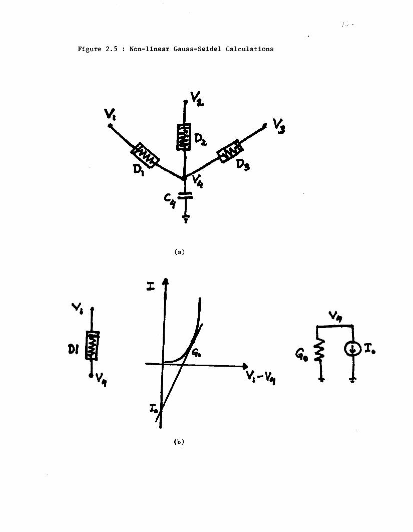
Figure 2.5 : Non-linear Gauss-Seidel Calculations

15
In circuit terms, the N-R calculation usually requires that a linear equivalent
be determined for each non-linear device connected to the node, as shown in
Fig. 2.5(b) for D1. This involves the calculation of a conductance, Go and a
current intercept, Io. In order to avoid the intercept calculation, we can
apply Eqn. (2-11) directly to Eqn. (2-12) to get
(2-13)
Now set AV&,f+1=V4(n)i+1-I,$ and substitute Eqn. (2-10) into Eqn. (2-13) to
W L
(2-14)
where V4(,)i refers to the i t h iteration value of voltage at Node 4 at time tn
and I j refers to the i t h iteration value of current a t Node j.. This method of
evaluating AT/ is convenient because:
0 no intercepts need to be calculated since total currents are used in Eqn.
(2-14)
current levels are within operating ranges (unlike Io in Fig. 2.5(b))
the value of A V is very accurate when calculated this way. Note that AV
is thz difference between two Newton iterations and it will tend toward
zero with each iteration. Therefore it should be calculated as accurately
as possible.
For an arbitrary node Eqn. (2-14) becomes
16
(2-15)
2.5.3. The SOR-EJewton Iteration
A combination of the Newton-Raphson iteration in a converged Gauss-
Seidel loop with acceleration applied is called an SOR-Newton Iteration. In
equation form, it is simply
(2-15)
In a standard N-R iteration, the equation is iterated until I A V I e . This
means that each node equation should be iterated to convergence before
moving on to the next one. The Gauss-Seidel loop (i.e.. the outer loop) must
also be iterated to convergence.
2.5.4. Convergence of the SOR-Newton Iteration
A very important property of the SOR-Newton iteration can be applied
now to greatly reduce the number of iterations of the inner N-R loop. I t hap-
pens that one Newton iteration per equation for each G-S iteration is
sufficient to retain the convergence properties of the non-linear Gauss-Seidel
iteration[l6] as long as the convergence requirements of the N-R iteration
are strictly satisfied.
A Newton-Raptison iteration will converge if the ~n lha l guess is "close
enough" to the exact solution, given b a t the function is Lipschitz continu-
ous. Under these conditions, the rate of convergence is quadratic. Since the
element model equations are smooth, the solution from one timepoint to t h e
next will not be drastically different. Therefore, the solution 22 , the previous

17
timepoint is a good first guess for the N-R iteration. Convergence may be
enhanced by using a prediction step based on the last few solution points. A
simple linear predictor is used in SPLICE using the previous two solution
points.
The diagonal dominance condition of the G-S iteration must also be
satisfied to guarantee the convergence of the SOR-Newton iteration. In cir-
cuit tcrms, this rcquiremcnt can always bc mct by putting a grounded capa-
citor at every node and choosing an appropriate timestep. Grounded capaci-
tors appear as -terms in the diagonal position of the conductance matrix
G. Therefore, h, which is the simulation timestep, can be reduced until the
C - term outweighs all off-diagonal terms. Obviously, the capacitance value, h
C, can be increased to achieve the same effect but usually the capacitance is
determined from the IC layout and therefore cannot be adjusted.
C h
Off-diagonal terms appear in the conductance matrix when there is cou-
C pling between two nodes. For example, when floating capacitors are used, - h
terms appear in diagonal and off-diagonal positions. Therefore, increasing
the value of C or reducing the value of h is not as effective and this may lead
to convergence problems. The ratio of the floating capacitor to the grounded
capacitor is an important factor in determining the speed at which conver-
gence is achieved. If the floating capacitor is very large compared to the
grounded capacitor, convergence speed will be slow, if the iteration con-
verges at all. The current version of SPLICE uses the IIE method (Implicit-
Implicit-Explicit) [25] to handle floating capacitors.

18
2.6. Implementation in SPLICE
The analysis techniques described in the previous sections have been
implemented in SPLICE1.6. The details are described in this section with
special attention given to areas where further optimization would improve
the simulator performance.
SPLICE1 has a Axed simulation timestep called the mrt {minimum
resolvable time). Events can only be scheduled a t integer multiples of mrt.
There is a scheduling threshold parameter called mindvsch which is the
minimum change in a node voltage over a timestep which causes the fanout
elements of the node to be scheduled. The convergence criteria is defined by
two parameters called abstol (absolute tolerance) and reltol (relative toler-
ance).
2.6.1. Program Flow
The program flow has not changed since the SPLICE1.3 release. The
details of the processing may be found in[l, 31 and are not repeated here.
The data structures of the ITA as implemented in SPLICE1.6 are given in
APPENDIX 11. The general program flow for electrical analysis is as follows:
set all nodes to their initial values ; schedule all FOL’s at time 0 ; #FOL = FanOut List of a node t,=O ; while ( t, < TSTOP ) f
foreach (FOL in the queue at the current timepoint)
foreach (output node of an element) t foreach (element in the FOL) f
process node : #see next section for details schedule FOL if necessary ;
1
plot all requested active nodes : t ,=t ,+l ;
19
2.6.2. Details of Node Processing
A subroutine in SPLICE1.6 processes all electrical nodes, calculates the new
node voltage, decides whether the node has converged m d determines
whether subsequent scheduling is necessary. A high-level pseudo-code
description of the routine is as follows:
begin # Iterated timing analysis algorithm in SPLICE1.6 # Node processing sequence
pick up next node i; if (first time processed at new timepoint) t
use last two points to perform linear prediction ; c onvflg = f alse ;
1 Gnet. = Tnet. = 0 ; for ( each fanin element at node i) t
compute equivalent conductance Geq; compute total current flowing into node leq; Gnet = Gnet + Geq; Inet = lnet + Ieq;
calculate AI' ; #charge in voltage over V @ ) t A V ; #new node voltage
DV = I V;t+l)-Vn-l I ; # change in node voltage over one timestep if (AV < tolerance) [ # node has converged
I i ter l t im
F
if (con* = false) f #have not converged at this timepoint before if ( DV > mindvsched ) f # node change is significant
schedule current fol at Tn+l (future) ; schedule fol of node at Tn (now) ; condig = true ;
1
1
else f # node change is not significant over one tiinestep Vn = Vn+l ; #restore old value
1 else #have converged previously at this timepoint
do nothing ; #break any feedback loops
else I # node has not converged so keep processing convflg = false ; schedule current fol at Tn (nouv) ; schedule fol of node at T, (now) ;
1
1

20
# Finished this node for this iteration return end
2.6.3. Element Mode l s
SPLICE1.6 has built-in models for resistors, linear capacitors (floating
and grounded), and MOS transistors. The TIE method is used to handle float-
ing capacitors [%] and the first-order Schichman-Hodges model [ Z S ] equa-
tions are used to handle the MOS transistors. The model equations used for
each of the devices are given in APPENUlX 111.
Each electrical element has a corresponding program subroutine. The
subroutine evaluates the linear equivalent model for each non-linear device
and returns it t o the calling routine. As mentioned previously, the intercept
current calculation can be avoided by a simple reformulation of the equa-
ticjns. Using this approach, the conductance and the t o t a l current at a given
operating point is returned by each subroutine. The calculation of the
equivalent model assumes that all other nodes have ideal constant voltage
sources attached to them.
2.7. ITA Simulation Results
This chapter has been concerned mainly with simulation accuracy and it
would not be complete without a comparison of ITA with SPICE2. Fig. 2.6
shows the simulation results obtained for the ring oscillator, 2-input NAND
and boot-strapped inverter circuits described earlier. As indicated by the
results, SPLICE1.6 produces results which are indistinguishable from those
obtained by SPICE2 except at Limepoints near time zero due t o difierent ini-
tial value assumptions. I t will be shown later in Chap. 4 that the 1'lA method

5
(b)
4
Boot-strapped
% = 0
+ 7 0
I
0 0
Figure 2.6 : Accuracy Comparison of SPICE2 and IT4
CLk-!
50 IQU
t tme (ns)
(a) Ring Oscillator
of Fig. 2.2(a)

J -
Figure 2.6 (c) : NAND circuit of Fig. 2 . 3 ( d )
4
3
I
0 0
t m e (ns)

21
is robust enough to handle complex analog circuits such operational
amplifiers in a unity-gain configuration. Therefore, circuits which handled
inadequately using NTA do not pose a problem to ITA in terms of accuracy.
The run-times of the 3 examples do not demonstrate the speed advan-
tage of ITA because the circu.its are all very small with dense G matricies and
the activity is high. The selective trace feature in SPLICE can only be used to
advmtagc in vcry largc circuits.
2.8. Optimizations in the Present Implementation
While the data structures used in SPLICE1 are well-suited to handle cir-
cuit, timing and logic simulation concurrently, they are not ideal for ITA. If a
separate program were written to perform ITA, several optimizations could
be made to improve the program performance.
For instance, some nodes are accidently reprocessed after they have
converged because there may be several paths to the same node through
different elements. Therefore, a node may be processed twice in succession
before another node is processed (i.e., two Newton iterations). Also, there is
a lot of time spent "walking" through the fanout lists and element tables to
reach a node, as shown in a previous section.
These problems can be eliminated by scheduling and processing nodes
as opposed t o fanout lists. A double buffcr schcmc at cach timepoint could
be used to avoid the accidental reprocessing of a node before all other active
nodes are processed, as follows:
put all nodes in event list EA(0) ;
while ( t, <TSTOP ) t , = o ;
k + O ; while ( event. list. El(t , ) is not empty ) t
foreach ( i in EA(tn) f

22
obtain AT/ : ut + =v:+A V ; if ( ) v r f l - w ~ ) l ~ ) 1 i.e., if convergence is achieved
else 1
add node i to list EA(tn+t) ;
add node i to event list EA(^^) ; add fanout nodes of node i to event list EA(^^)
if they are not already there ;
j
f
Another problem in the current program is that if it does not converge
at a timepoint, the program simply stops execution. The user must decrease
the timestep manually and re-run the entire simulation. An automatic inter-
nal timestep control mechanism would be useful not only for the conver-
gence problem but also for error control. E the error is small at a particular
timepoint, then the timestep could be increased. If the error is too large,
the timestep could be decreased. The nodes would then be re-evaluated at
the new timepoint. Hence, the timestep could be computed based on a n esti-
mate of the Local Truncation Error. Each node could have its own mrt,
independent of other nodes, as long as some consistency is maintained in the
simulation between different nodes. Unfortunately, dynamic timestep con-
trol requires the ability to “backup” in time (Le., a buflering of previous
results for each node) and requires a modification of the data structures to
allow successive refinement of the mrt (minimum resolvable time) in the
time queue [27] . For this reason, it would require a lot of effort to imple-
ment this scheme in the current SPLICE1 environment.

23
3. Mancements to the Logic Analysis
3.1. Introduction
The improvements made to the logic analysis in SPLICE1 are described
in this chapter. The starting point of this work was SPLJCE1.3. I t had the fol-
lowing features:
a 4-st.at.e logic model (0,1,X,7,)
fixed assignable rise and fall delays on all gates
unidirectional and some bidirectional elements hmdled.
There have been a number of changes in the logic analysis since the
SPLlCE1.3 release. These changes were made to alleviate some of the prob-
lems in the previous version and to facilitate conversions in the mixed-mode
envi-onme nt.
The new version is SPLICE1.6 which features:
a new MOS-oriented state model
a fanout dependent delay model
unidirectional and generalized bidirectional element processing.
The logic analysis is performed using a relaxation-based method, similar
in nature to the electrical analysis. In fact, the logic analysis can be thought
of as an implementation of non-iterated timing analysis (see Chap. 2) with
simplified element models. Each logic node carries information about the
node voltage and the equivalent conductance-to-ground, as does the electri-
cal node. Tnerefore, the mixed-mode interface is defined in a consistent
manner in SPLICE1.6.

24
This chapter begins with a description and definition of the new state
model. Following this, the delay model is described. Then, the "spike" detec-
tion and handling procedure is presented. A spike is a pulse at a node of
shorter duration than the minimum width necessary to trigger subsequent
gates. This is usually an error condition which must be identified. and
reported t o the user.
In the next section, thc important issucs surrounding thc MOS transfer
gate a re reviewed. The transfer gate (or transmission gate, or pass transis-
tor) is the source of all MOS modeling problems at the logic level and the rea-
son for this will become clear in this chapter. Next, the logic analysis algo-
rithm wil l be presented in detail. SPLICE1.6 can also be used t o perform
switch-level simulation [9, 101 and this is described in the last section. Back-
ground material on MOS logic simulation may be found in reference[3].
3.2. The State Model
3.2.1. A MOSoriented bgic Model
Most modern logic simulators handle the problems specific to MOS
integrated circuits by including the notion of s$nd strength[?, 8,9,10] in the
logic model. The rationale for this has been presented in a previous publica-
tion[3] . Strength is an abstraction of the large-signal conductance from a
node t o ground or from a node to a supply voltage. I t can be associated with
the output of a gate or it can be an attribute of a node. For instance, in the
inverter of Fig. 3.1 (M1 and MZ), the driver transistor with its gate input at
5.0V represents a very low resistance path from Node B to ground. In MOS
logic model terms, this is referred to as a "forcing 0" or "driving 0". Simi-
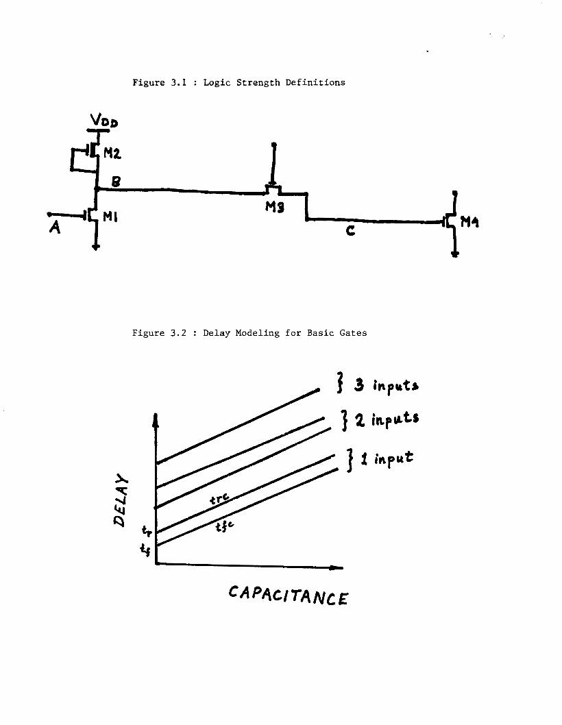
Figure 3.1 : Logic Strength Definitions
Figure 3.2 : Delay Modeling for Basic Gates

25
larly, the load transistor represents a sizeable resistance from Node B to WID
(approx. 20kR to 40kR) and this is referred to alternatively as a "soft l", a
"resistive 1" or a "weak 1". If transistor M3 is turned "OFF" (that is, if the
gate voltage is zero for an NMOS transistor), Node C goes into a "high-
impedance" condition which represents a third distinct strength. Although
most simulators are based on these three strengths, SPLICE1.6 allows up to
2lS -1 strengths for two reasons:
there is a requirement for more than thrze strengths when modeling the
interaction of several transfer gates with difr'ering IY/L ratios, typically
found in bus contention situations.
it provides a mechanism for consistent signal representation in the logic
domain for schematic or mixed-mode simulation[22] . If information
about the effective conductance to ground is stored with each electrical
node, this information could be converted to a strength value and
passed on t o the logic node, along with the voltage information, when-
ever there is a requirement to do so. Conversions in the opposite direc-
tion can be performed in a similar manner. In this way, simulation
accuracy can be maintained in the mixed-mode environment.
3.2.2. State Model Definition
The state model used in SPLICE1.6 is now formally defined :
A state is composed of a logic level, logic strength pair (L,S).
i. e., stat e = (L, S) = (Leve 1, St re ng th)
The logic level can be one of three values: logic zero(O), logic one(1) or
logic unknown(X). The " 0 ' level represents the low threshold value or
ground. The "1" level represents the high threshold value or VDD. The

26
"X' level represents an undetermined value which could be "0". "1" or
some value in between. The logic level fleld is extracted from the state
using the "lev" function. That is,
L = lev(state)
The logic strength is an integer value between 1 and some user-specified
upper limit. The upper limit has a maximum allowed value of 65,536. In
this rcport, thc subscripts f , ~ and z will be uscd to dcnote the largest,
middle and smallest strengths respectively in a given range. The
strength field is extracted from the state using the "str" function. That
is,
S = str(state)
A n initial unknown, &, must be distinguished from a unknown generated
during the analysis, X,. This is done in SPLTCE1.6 by defining the initial
unknown as follows :
X = lev(initid-unknown)
o = str(initia1-unknown)
and the generated unknown as follows:
X = lev(generated-unknown)
0 # str(generated-unknown)
The initial unknown is useful to identify nodes which are not exercised
by the input pattern used in a simulation. As a post-processing step,
these nodes could be reported to the user.
3.2.3. Using the State Model
In a logic anaiysis, nodes are scheduled to be processed in the time
queue in accordance with the activity in the circuit. When a node is

27
processed, the fanin list (FIL) is obtained from the node data structure (see
Appendix 11, parts 1,Z) . Each gate in the fanin list is a potential driver of the
node (by definition) but usually only one gate will gain control of the node
and determine its final state. The gate with the largest output strength is
declared the "winner" and the node adopts the output state of the winning
gate. Node contention occurs when two or more gates attempt to drive the
same node to different logic levels with the same driving strength. In this
case, the node is assigned an X level and the driving strength of any one of
thc contcnding gatcs. Thc proccssing dctails zrc prcscr,tcd in Scction 1.6.
3.3. The Delay Model
3.3.1. Factors AfTecting Switching Delay
Once a new state is determined, the next task is to calculate the time
required to reach the new state. In MOS circuits, the switching time is based
on many factors which include:
the basic gate switching time (unloaded)
the static output loading due to capacitance of elements connected to
the node
the dynamic output loading through transfer gates which are turned
"ON" (that is, transistors with their gates at the logic "1" level)
the number of gate inputs
the shape (rise and fall times) of input waveforms
N o logic simulator attempts to incorporate all of the above factors into
.the delay calculation. On the other hand, it is essential that a logic simulator

28
include all the first-order effects in the delay calculation. SPLICE1.6 is capa-
ble of handling the first four factors. The fifth factor (input waveform shape)
is more difficult t o handle at the logic level and is usually considered a
sec on d-or de r effect .
3.3.2. Delay Model for Simple Gates
The usual modeling procedure for logic simulation is to generate a set of
curves similar to Fig . 3.2 for every primitive element (NANDs, NORs, invert-
ers, etc.) using accurate electrical simulation. In this figwe, the delay from
the input switching point to the output switching point is plotted as a func-
tion of output loading and the number of inputs. Although not strictly true,
the relationships are taken to be linear. The y-intercept of each curve
represents the intrinsic unloaded gate delay while the slope of each curve
represents the gate drive-capability.
Assuming that the above information is available, the following method
can be used to calculate delays for simple gates. The first requirement is
that a capacitance value be specified on every input and output pin of every
gate as part of the model definition. Then the total gate delay can be
represented by four parameters : the intrinsic gate delays (tr, t f ) and the
gate drive-capabilities (trc, tfc), where
*=rise time for unloaded gate (intercept)
tf =fall time for unloaded gate (intercept)
trc =gate drive-capebility for rising signals (slope)
t f c =gate drive-capabiEty for faliing signals (slope)
Using these values, the total delay is caicalzted using the equation:
Figure 3 . 3 : Node capac i t ance pre-processing
%=-
29
risetime = t r + t T C + (node capacitance ) (3-la)
f a l l t h e =tf +tf c+(node capacitance) (3-lb)
The node capacitance value is extracted in a pre-processing step by
summing the capacitances of all elements connected to a node, and stored
with the node data structure (see APPENDIX 11, part 1). This process is illus-
trated in Fig 3.3.
3.3.3. Delay Model for Yulti-output Elements
If a multi-output element, such as the flip-flop shown in Fig. 3.4(a), is
available as a primitive logic element, each output would have its own set of
curves similar to Fig 3.2. -The curves for the Q and QB outputs of the flip-flop
are shown in Fig. 3.4(b). Then 4N parameters would be required to specify
the delay, where N is the number of outputs. For the Aip-flop there would be
8 such parameters : Qtr, Qtf, QBtr, QBtf, Qtrc, Qtfc, QBtrc, and QBtfc. These
parameters would be applied to Eqn. (3-1) to calculate the delay. Using this
technique, the delay associated with each output could be handled indepen-
dently. The overriding assumption is that the rise and fall drive-capabilities
(trc,tfc) of the outputs are constant and independent of the inputs.
In some elements, the delay from a particular input (say. the RESET pin
of the flip-flop) to some output (either Q or QB) is different from another
input to output delay (J- or K-input t o output delay). This suggests that, in
fact, the intrinsic delay should be a matrix which is indexed by input pin
which initiates activity and the output pin being processed. Then the total
delay due to loading could be calculated using Eqn. (3-1) and the specific trc
and tfc values for each output. This is shown in Table 3.1 below for the flip-
flop example.
>.
F i g u r e 3 . 4 : JK F l i p - f l o p Circuit
a Q t Q B

Table 3.1 Intrinsic Delay Matrix 30
t f = l O t f = l O t f = l O tr=lO tr=lO tr=lO tr=5 tr=5 tf=ll t f = l l t f = l l tf=6 tf=6
3.3.4. Delay Models for Transfer Gates
The delay calculation for logic circuits containing transfer gates is more
complex than either of the two cases given above. Consider the circuit of
Fig. 3.5. The delay from Node A to Node B when the input CLK of the transfer
gate makes a transition from "0" to "1" is based on:
the W/L ratio of the transfer gate
the drive-capability of gate INV
charge-sharing between C 1 and C2
I t is a highly non-linear situation and therefore difficult to model in
logic. Charge-sharing cannot be represented properly because of the voltage
resolution. One way to handle it is by allowing multiple voltage levels similar
to the way that the three impedance levels have been extended. This would
facilitate the characterization of charge-sharing but would complicate the
simulator. The simulator would have to handle transitions from one voltage
level to another in a consistent manner. SPLICE1.6 lumps all the non-linear
effects into two values called the turn-on (ton) and turn-off (toff) times.
These values do not take capacitive effects into account.
Another delay modeling issue concerns transfer gates connected in
series as shown in Fig. 3.6. The delay in question is that from Node A t o Node
E. If all gates are "ON", the circuit can be represented by an RC transmission
line. Unfortunately, this is difficult to model an the logic level. A few alterna-

Figure 3.5 : Non-linear Effects due to Transfer Gates
Figure 3.6 : Delay modeling for series-connected MOS Transfer Gates

31
tives exist to handle this situation:
Use a zero delay model across transfer gates when they are “ON” [e] . This is the method used in SPLICE1.6. Unfortunately, the value of delay
calculated this way is too optimistic a Node E.
Lump capacitances C1, CZ, C3, C4 and C5 together and use this value in
eq. (3-1). This is the transition delay for all nodes from the old state to
the new one. The value of delay calculated this way is too pessimistic a t
Node A.
Extend the notion of drive-capability of a gate to nodes other than its
output node. Since txl is “ON”, both Node A and Node B are driven by
gate INV. Therefore, the delay to A could be calculated as given in eq.
(3-1) and the delay to B could be calculated using the equation:
riset ime =trcINv* (capacitance at B ) (3-2a)
f a l l t i m e =tf CINV* (capacitance at B ) (3-2b)
To compute the delay to nodes C, D and E, simply apply eq. (3-2) again
using the capacitance a t node C, D and E respectively. This approach is
bet ter than either of the above methods but is still lacking in accuracy
because it does not account for the ”ON” resistance of the transistors.
One modification which may provide more accuracy is to adjust the
values of t rc and t fc using the “ON” resistance of the transfer gates and
the depth of the node away from the output of the controlling node. This
method is promising because VLSI circuits typically contain intercon-
nections which a re electrically equivalent to distributed RC transmission
lines. They could be handled exactly the same way as the set of series
transfer gates. Therefore, a netlist extractor could provide the simula-
tor with ”UELAY” elernents,as shown in Fig 3.7, in place of interconnect
32
with delay calculations performed using the modfled eq. (3-2) :
r iset ime = TRCC(capacitance ut n o d e )
f aufime =TFC(cupac i tance at n o d e ) where
TRC=trc+f ( r e s i s t m c e , d e p t h )
TFC=tfc*f (resis tance ,depth)
3.3.5. Delay to an Unknown Value
The delay calculations in the previous section assume signal transitions
. Nodes may, of course, acquire the X level due to from ”0” to ”1” or “1” to ”0”
contention at the node as described in an earlier section. The question then
arises as t o when the X level takes effect. The unknown level could be ”O’, “1”
or some intermediate value. Clearly, if the unknown is the previous value,
there is no delay. If it is the opposite logic level there is a rise or fall transi-
tion delay. The usual approach is to assume that the unknown value takes
affect immediately (as is done in SPLICE1.6) or one time unit in the future.
3.4. SpikeHandling
SPLICE1.6 uses an inertial delay algorithm. This means that if a node is
scheduled to change at some time in the future T,, it is held at its old value
until that time. Then at T,, the new value is assigned t o the node and the
fanouts of the node are processed using this value. A spike (commonly
referred t o as a glitch) occurs if the node is scheduled to change to a
different value before it reaches the new value. Spike detection is simple in
true-value logic simulation but becomes very complicated when performing
fault. simulation. When a spike is detected, the event a t T, is dropped, the
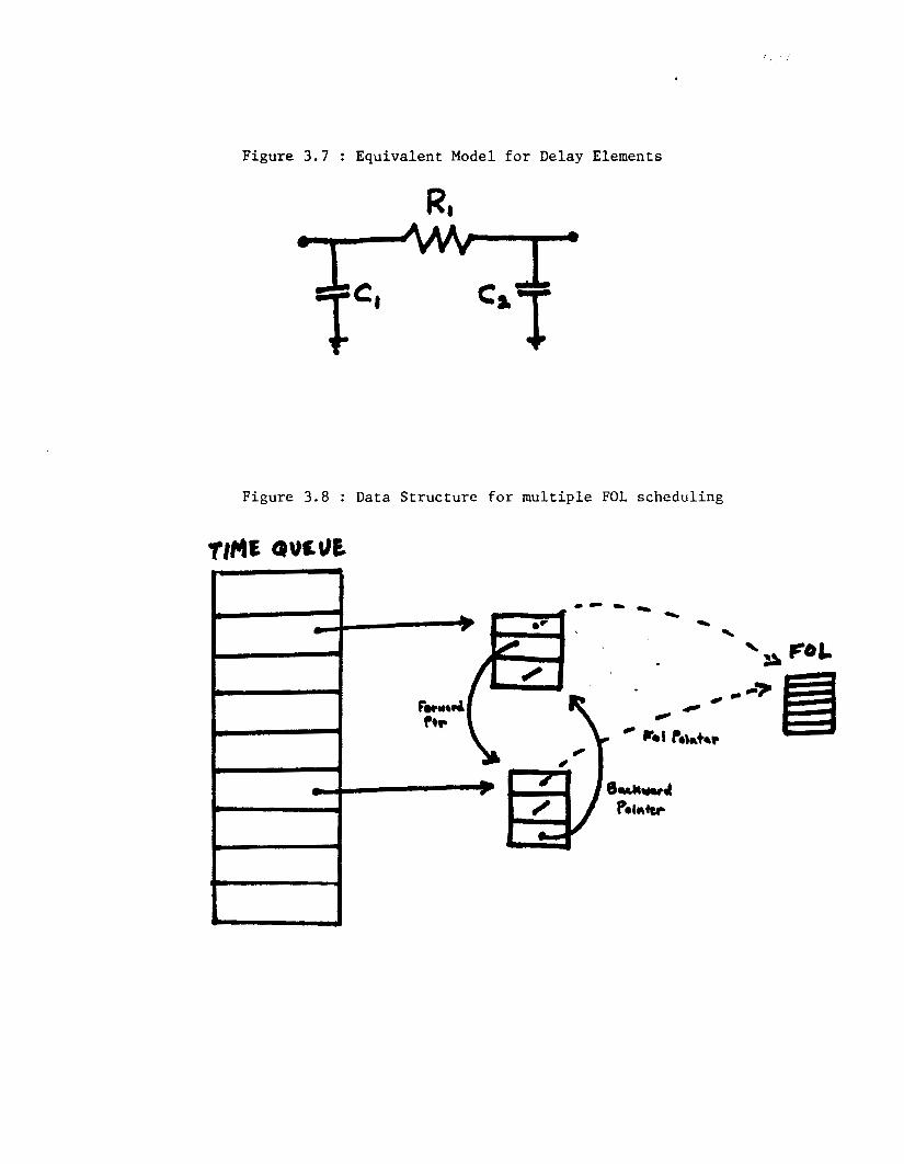
Figure 3.7 : Equivalent Model for Delay Elements
Figure 3.8 : Data Structure for multiple FOL scheduling

33
new event is scheduled at the appropriate time and the user is notified of the
glitch. The glitch is not propogated because it usually signifies an error in
the circuit design. Therefore, the simulation will continue as if an error did
not occur and more meaningful information may be obtained about the
correct operation of circuit. This technique also reduces the amount of work
the simulator is required to do because spikes represent activity in the cir-
cuit. Therefore, the overall CPU-time will be kept to a minimum by removing
glitches from the simulation.
In SPLICEl.6, a fanout list (FOL) can only appear once on the time queue
at any given time during the processing. This is a limitation for proper glitch
handling, as will be seen in the psuedo-code description of glitch handling
which follows. Two different problems are identified which are direct results
of the scheduling limitation.
#GLITCH HANDLER IN SPLICEl.6 PT = present time Tnezt = next time FOL is scheduled qast = last time FOL was scheduled to be processed
(or was actually processed) if ( Trmt c PT) { #node was processed in the past
store new-state ; schedule FOL at TMzt ;
= PT) t #node is scheduled now
if (FOL processed) [ # PROBLEM : glitch has been propogated
I if Tnezt2 Tl& 1 t if ( VWt
update new-state ; schedule FOL at TWzt :
else f #FOL has not been processed #PROBLEM : cannot schedule FOL more than once
drop schedule at TLast : replace new-state ; schedule FOL at TWzt ;
I
I 1 else if ( Tlast > PT) f #node is scheduled in the future
if (Tnezl < Tht 1 I #reschedule time is earlier than originally scheduled time
report glitch : drop schedule at TLast ;

34
replace new-state : schedule FOL at Tnezt ;
I else if ( Td = Tlmt) f
report glitch : replace new-state ;
1 else if ( Tnszt > Tbt) f #want to sched in future
report glitch ; drop schedule at T- ; store new-state ; schedule FOL at T,, :
! I
The problems identified above can be summarized as follows: depending
on the order in which nodes are processed at a timepoint, the program may
or may not propagate the glitch. Therefore, the output of the simulation
depends on the order in which the circuit was specified by the user. The
glitch is always identified but its propogation is based on node processing
order. One way to get around this problem is to use a two-pass approach by
first performing a Leveling operation [2!3] as a preprocessing step. This sim-
ply means that each node should be assigned a value based on its depth from
the inputs. Then every node scheduled at a given timepoint should be pro-
cessed in ascending order. . This would incur some overhead but would pro-
duce the desired results, Le., the same solution regardless of the order of
the input description. At the present time, SPLJCE1.6 will identify the glitch
and may or n a y not propagate the glitch depending on the order the nodes
are processed.
Another way to eliminate the problem is by modifying the scheduler
data structure so that multiple schedules are allowed. Instead of scheduling
FOLs, it would be better to schedule structures which point to the FOL. This
structure would have to include other information such as the schedule time,
and forward and backward pointers to the next and previous schedules of the
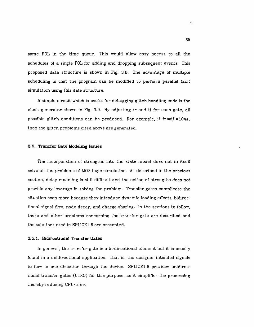
35
same FOL in the time queue. This would allow easy access to all the
schedules of a single FOL for adding and dropping subsequent events. This
proposed data structure is shown in Fig. 3.8. One advantage of multiple
scheduling is that the program can be modified to perform parallel fault
simulation using this data structure.
A simple circuit which is useful for debugging glitch handling code is the
clock generator shown in Fig. 3.9. By adjusting tr and t f for each gate, all
possible glitch conditions can be produced. For example, if tr=tf = l W ,
then the glitch problems cited above are generated.
3.5. Transfer Gate M o d e l i n g Issues
The incorporation of strengths into the state model does not in itself
solve all the problems of MOS logic simulation. As described in the previous
section, delay modeling is still difficult and the notion of strengths does not
provide any leverage in solving the problem. Transfer gates complicate the
situation even more because they introduce dynamic loading effects, bidirec-
tional signal flow, node decay, and charge-sharing. In the sections to follow,
these and other problems concerning the transfer gate are described and
the solutions used in SPLICEl.6 are presented.
3.5.1. Bidirectional Transfer Gates
In general, the transfer gate is a bi-directional element but i t is usually
found in a unidirectional application. That is, the designer intended signals
to flow in one direction through the device. SPLICE1.6 provides unidirec-
tional transfer gates (U'IXG) for this purpose, as it simplifies the processing
thereby reducing CPU-time.

Figure 3.9 : Circuit used to generate all possible Glitch conditions
Figure 3.10 : A bi-directional Transfer Gate Model

36
On the other hand, there are occasions when transfer gates are used in a
bidirectional application and therefore the logic simulator must be able to
handle them. There have been a variety of modeling approaches for bidirec-
tional transfer gates (BTXG), including the conventional approach of two uni-
directional elements back-to-back as shown in Fig. 3.10. This approach can
lead to inconsistencies when different logic values are on opposite sides of
the element, as is the case in Fig. 3.10. Each value can flow through the
BTXG and reach the opposite side and these errors can percolate further
through thc circuit producing incorrcct rcsults. Thcrc arc ways to gct
around this problem but they can be very complicated. One way to handle
BTXG's in a consistent way is to introduce the concept of composite node
relaxation (CNR). In this method, every node connected through transfer
gates which are "ON" are considered to be the same node for processing pur-
poses. All fanin lists for the composite node are combined into one list and a
new state is determined based on the composite fanin list. Since all nodes
connected by "ON" BTXG's a r e considered the same node, there is no delay
between them.
3.5.2. Unknowns at Gate Inputs
Another problem in modeling transfer gates is handling unknowns at
gate inputs. The problem is identified in Fig. 3.11. Normally, if the transfer
gate is "ON' and then shuts "OFF", the output Node A retains its previous
value but is reduced in strength (goes to the z strength). This is shown in
Fig. 3.11(a). There are three cases to consider in conjunction with unknowns
at transfer gates.
CASE 1 : Fig. 3.11(b) indicates the situation at the beginning of the simula-

37
tion. Virtually all gate inputs, except for the ones that have been initialized
explicitly, are in the initial unknown condition. In this situation, the gate
may or may not pass signals.
CASE 2 : The second situation occurs when there is a logic "1" at the input
and it becomes a logic "X". In this case, the level at the output remains the
same but the strength is not known. This is illustrated in Fig. 3.1l(c).
CASE 3 : The third situation is the reverse of the second. Here, the input
gocs from logic "0" to logic '3". Both thc valuc and strcngth may changc.
This is shown in Fig. 3.1l(d).
There are a few alternative methods to handle unknowns at gate inputs.
(1) a pessimistic approach is to generate X, at the output so that it wil l be
propogated further. This may produce incorrect circuit operation if
CASE 2 is considered, but is the easiest to implement.
(2) another approach is to have the notion of unknown strengths. Using this
model, CASE 2 could be handled by setting the output node to its previ-
ous value with an unknown strength. This introduces some complications
in the way the simulator processes nodes. Some bit pattern would have
t o be selected for unknown strengths. I t is not clear how this special
strength value would interact with other strengths.
(3) assume that devices are "CN" and process nodes. Then turn devices
"OFF' and reprocess nodes. If conflicts result at any nGdes, then set
them t c "X". If no conflicts occur, then set nodes to correct level and a
pessimistic strength [ z ~ J .
Currently. method (1) is used in CPLlCE1.6 and methods ( 2 ) and (3) are
k i n g k - c s t i g atcd furthcr .

I T 1
J m
(b) CASE 1
( c ) C A S E 2 ( d ) C A S E 3
Figure 3.11 : Handling Unknowns at gate inputs

38
9.5.3. Node Decay
When a node acquires the z strength, it retains the previous state on the
capacitance at the node. Physically, charge is trapped at the node and there
are parasitic resistive paths from the node to ground or VDD. Therefore, the
node will eventually lose its value and it will become unknown. This is
referred to as node decay. The time constant for the decay is large but
finite.
I t is useful to include node decay as part of the simulation, especially for
dynamic circuits. One way to do this is to detect the z strength at a node
and schedule the node to decay after a specified amount of time by setting a
special flag a t the node. If the node is not refreshed before this time, the
node is placed in the unknown state. If the node is redriven, the scheduled
event would be dropped and processing would continue. Unfortunately, the
program would incur an excessive amount of scheduling and de-scheduling
overhead, especially in the case of dynamic MOS circuits. Moreover, in
SPUCE1.6, most of the scheduled nodes would be put into the pool (see
Appendix 11, part 5). The pool is an overflow area designed to handle all
schedules which are greater than 200 timepoints in the future. This would
always be the case for node decay. Clearly this is not a suitable approach.
A n alternative approach, proposed by Boyle [30], is to simply store the
decay time along with the node data structure and avoid scheduling alto-
gether. Everytime the node is redriven, this value could be compared to the
current time. If the current time is greater than the decay time, a warning
message could be sent to a file if the user has requested it. Then processing
would continue as if node decay had not occurred, I t is not useful to sirnu-
late the circuit under decay conditions because it is usually a design error.

39
Therefore, as was done in glitch handling, it is simply flagged as an error and
then ignored for the remainder of the simulation.
3.6. bgic Simulation Implementation Details
3.6.1. General Program Flow
The following is a high-level psuedo-code description of the general pro-
gram flow during a logic analysis. Note the parallel between the ITA program
flow described in the previous chapter and the code below:
set all nodes lo h e i r inilial values ; schedule all FOL's at time 0 : # FOL = fanout list
while ( tn': TSTOP ) { tn=o;
for (each FOL in the queue at the current timepoint)
for (each output node of an element) [ for (each element in the FOL ) f
process node ; #see next section for details schedule FOL if necessary ;
1 1
1 t n + t n + I ; plot all active nodes ;
1

40
3.6.2. Node Processing Details
# LOGIC NODE PROCESSING DETAILS # begin
currentstate e (X,O) ; place node in CNL : # CNL = composite node list for (each node in the CNL) f
for (each element in the FIL) # FIL = fanin list if (element = BTXG) & (gate = “ON”)
place node in CNL : I else t
determine output-state (L.S) of element : intend-state e output-state :
1 if ( str(intended-state) > str(current2tate) )
current-state intended-state : else if ( str(intended-state) = str(current-state) )
if ( lev(intended2tate) # lev(current2tate) ) lev(current_state) 6 X :
1 1 new-state 6 current-state if (new_state # old_state) f
for (each node in CNL) 1 calculate delay(old_state,new_state) : call GLITCH HANDLER to schedule FOL ; # FOL = fanout list
1 end
3.7. Switch-level Simulation
The definition of UTXG and BTXG elements allows a switch-level simula-
tion [9, 101 to be performed using SPLICE1.6. Loads can be modeled using a
UTXG with a “soft” output strength. Drivers can be modeled using a UTXG
with a “forcing” output strength. Either a BTXG or a UTXG can be used for
pass transistors depending on the application. Other floating transistors
must be BTXG’s. If ”ton“ and “toff’ are specified as 1 unit of time, then a
unit-delay switch-level simulation will be performed by SPLICE1.6. An
interesting parallel can now be drawn between the electrical and logic simu-
lators in SPLICE1.6. The processing sequence is exactly the same in both

41
cases. Only the resolution of the voltage levels and the transistor models are
different. Unfortunately, there is no timing information in the transistor-
level logic simulation. If timing information could somehow be included in a
switch-level simulation, then mixed-mode simulation at the transistor would
be quite feasible. For obvious reasons, delays at the switch-level cannot be
handled the same way as it is currently done is SPLICE1.6 for standard
boolean gates. Three approaches have been proposed to introduce timing
information a t the switch-level [31, 32, 291 using a resistive simulation model.
Thcsc mcthods arc undcr investigation at thc prcscnt time.

42
4. Examples and Results
This chapter presents a number of simulation results and program perfor-
mance statistics of SPLICE1.6. Five aspects of the program are examined in
the sections to follow. These are :
the program performance statistics such as processing speed for electr-
ical and logic nodes, typical storage requirements per element, iteration
counts ,etc.
the identification of bottlenecks using profilers
the factors which affect the run-times such as mindvsch, sor, mrt and
floating capacitors
SPLICEl/SPICEZ comparisons for execution speed and memory require-
ments
the program’s ability to handle analog circuits
The simulations were carried out using two large digital circuits, one
small analog circuit and one small digital circuit. They were as follows:
(1) Digital Nter Circuit : This circuit was obtained from[l] . I t is an
integrated circuit which performs a digital filtering function. There are
705 MOS transistors and 393 nodes in the circuit. The simulation period
is 4ps.
(2) Counter-Decoder-Encoder Circuit : This circuit is a combination of a 4-
bit counter driving a 4:16 decoder and B 16:4 encoder. I t will be
rererred l o as the C X circuit in Lllc res1 of llle c l iq t c r . Tlie swilching

(3)
(4)
4.1.
43
times were based on the specifications provided in a TTL Handbook [33] . The circuit has 1,326 MOS transistors and 553 nodes. The simulation
period is also 4ps[34] .
NMOS Operational Amplifier : This circuit was obtained from E351 . I t
was used as part of a phase-locked loop circuit. Fig. 4.4(a) is a
schematic diagram of the MOS operational amplifier (oparnp). This cir-
cuit is used to illustrate the capability of ITA in handling analog circuits.
Bootstrapped Inverter Circuit : This circuit was described earlier in
Chap. 2. I t is illustrated in Fig. 2.4. The circuit is used to examine the
degradation effects of a floating capacitor element in an ITA simulation.
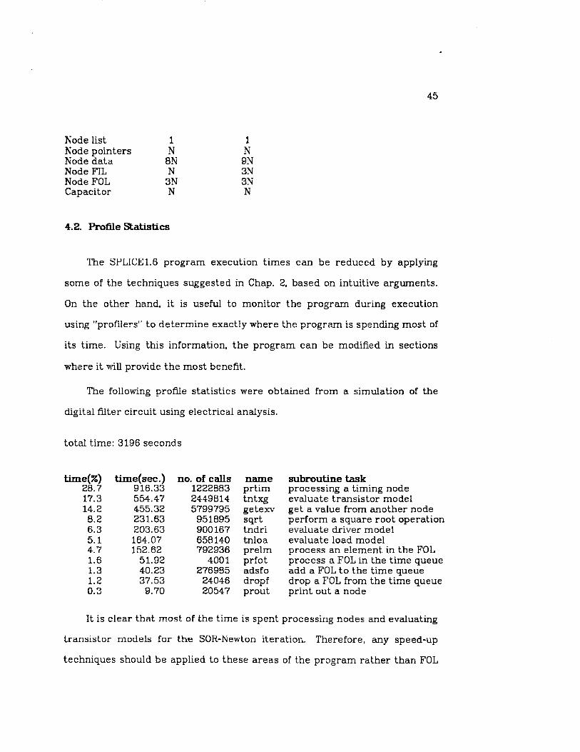
Program Performance Statistics
In order to predict the run-times and memory requirements of the pro-
gram SPLICE1.6, the program execution speed and memory usage statistics
are required. These statistics have been tabulated below for both the electri-
cal and logic simulztors.
Electrical Simulation Statistics
Node Evaluations 600 nodes/sec. SOR-Newton Iterations (no floating caps) SOR-Newton Iterations (with floating caps)
3-5 iterations/node 6-20 iterations/node
ELectrical Element Storage Requirements
Elements Tme Words Required Transistors Load 3 x no. of loads
4 x no. of drivers 5 x no. of transistors
3 x no. of capacitors
Driver Trans is tor
13o ating Capacitors Grounded 0

44
hs i s to r s 3 x no. of resistors
Element Model Type Words Required Transistors h a d 11 x no. of loads
11 x no. of drivers 12 x no. of transistors
Capacitors Grounded 1 x no. of grounded capacitors 3 x no. of floating capacitors
Resistors 3 x no. of resistors
Driver Transistor
Floating
bgic Simulation Satistics
Node Evaluations 650 nodes/sec.
bgic Element Storage Requirements
Elements Words Required
inverter 3% no. of inverters buffer Ah’D O R NA??D NOR XOR XYOR transfer gates
3 x no. of bufIers -15 x no. of APU’Ds -:5 x no. of ORs -i5 x no. of NAKDs -5 x no. of NORs -i5 x no. of XORs -.5 x no. of XRORs * 4 x no. of devices
Model Type invert e r buffer AKD OR NAND NOR XOR XXOR transfer gates
Words Required 11 x no. of different inverter models 11 x no. of different inverter models - 11 x no. of different AND models - 11 x no. of different OR models - 11 x no. of different KAND models - 11 x no. of different NOR models - 11 x no. of different XOR models - 11 x no. of different XNOR models -18 x no. of device models
Node Storage Requirements
N = number of circuit nodes
Data Logic Node Electrical Kode
45
Node list 1
Node data 8 N Node FIL N Node FOL 3 N
Node pointers N
Capacitor N
1 N 9N 3 N 3 N N
4.2. Profile Statistics
The SPLICE1.6 program execution times can be reduced by applying
some of the techniques suggested in Chap. 2, based on intuitive arguments.
On the other hand, it is useful to monitor the program during execution
using ”profilers” to determine exactly where the progran is spending most of
its time. Using this information, the program can be modified in sections
where it will provide the most benefit.
The following profie statistics were obtained from a simulation of the
digital filter circuit using electrical analysis.
total time: 3196 seconds
time(%) 28.7 17.3 14.2 0.2 6.3 5.1 4.7 1.6 1.3 1.2 0.3
time(sec.) 9 16.33 554.47 455.32 231.63 203.63 164.07 152.62
51.92 40.23 37.53 9.70
no. of calls 1222883 24498 14 5799795 951895 900 167 658 140 792936
400 1 276985
24046 20547
name prtim tntxg getexv sqrt tndri tnloa prelm prfot adsfo dropf prout
subroutine task processing a timing node evaluate transistor model get a value from another node perform a square root operation evaluate driver model evaluate load model process an element in the FOL process a FOL in the time queue add a FOL to the time queue drop a FOL from the time queue print out a node
I t is clear that most of the time is spent processing nodes and evaluating
transistor models for the SOR-Newton iteration. Therefore, any speed-up
techniques should be applied to these areas of the program rather than FOL

46
processing, node printing, etc.
4.3. Factors Affecting Execution Time in Electical Simulation
4.3.1. WU-time vs. MRT
SPLICE1.6 has a user-specified fixed simulation timestep called the mrt
(Minimum Resolvable Time). The symbol h will be used to refer to the
timestep associated with a particular node. In SPLICE1, h is some integer
multiple of mrt. Although the simulation timestep is fixed, the value of h for
a specific node is dependent on the activity at that node. For example, when
the node is active, h is equal to mrt. Otherwise, h is defined by the time
difference between two events a t the node. In a sense, the timestep at a
node is determined implicitly by the activity in the circuit.
Since there is no explicit dynamic timestep control in the SPLICE1, the
CPU-time required to perform an electrical simulation is dependent on the
value chosen for mrt. Fig. 4.1 illustrates this relationship for the CDE cir-
cuit. There is a definite optimum value of mrt for this particular circuit and
this holds true in the general case. At values of Lnrt greater than the
optimum value, there are two effects occurring simultaneously :
the diagonal dominance condition of the conductance matrix is weak-
ened by the fact that the ---terms in the diagonal are smaller; there- C h
fore, the program will iterate longer to obtain a consistent solution ;
the difference between the solution at a time t , and t ,+l increases as
mrt increased and so the Newton-Raphson convergence rate may be
linear instead of quadratic.

F i g u r e 4.1 :
CPU-time vs mrt
F i g u r e 4
CPU-time vs.
2 :
mindvsch
I I I I
3 QI W
m 0 6'1 -
0.a + I I I 1
*4 -6 e0 0 .L
mindvsc h ( v o h s )

47
At mrt values less than the optimum, the program is forced to do more
work during the active periods than is really necessary, based on the time
constants in the circuit. Therefore, there is a rapid rise in the curve in Fig.
4.1 at small values of mrt. I t has been observed that at very small timesteps,
the curve begins to level off. This is probably due to the fact that the predic-
tion step is very accurate and only one or two iterations are required for con-
vergence.
The relation between CPU-time and mrt suggests that, for a given tech-
nology. the optimum value should be obtained through experiment and used
in all further simulations. Of course, if an explicit dynamic timestep control
mechanism is implemented, this would not be necessary.
4.3.2. CPU-time vs. MINDVSCH
In SPLICE1, events at a node are propogated to its fanouts if the change
in the node voltage is considered to be significant. If the change is not
significant, the fanouts are not, pchpd.~i !~r l s n d the node i s rstiimed to its ori-
ginal value. This constitutes the event-driven selective-trace feature in
SPLlCE1. The scheduling threshold parameter, used to determine whether or
not the change is significant, is called mindvsch. I t is specified in units of
volts, by the user, for an entire simulation and is the same for every node in
the circuit.
The value chosen for mh-ch has a profound effect on simulation
results. Careful consideration must be given to select an appropriate value
for this parameter. I t can be thought of as the minimum voltage change
whch can affect the fanout elements of a node. Therefore, an upper bound
for digital circuits is the threshold voltage, V,, usually in the order of 1V.

48
The lower bound on mindmch is the value used to determine convergence at
a node, called abstol, which is typically 1pV. Therefore, a value of mindvsch
lies in the range from l p V to 1V. Based on experience with the program, an
appropriate value for most digital circuits is 1mV.
The effect of minhch on CPU-time is quite dramatic as shown in Fig.
4.2. As mindvsch is increased, the CPU-time goes down. This suggests that
thc valuc should be madc as large as possiblc. Unfortunatcly, some
significant events may be accidently dropped if the mindvsch is too large
resulting in a loss of accuracy. Also, node voltages can only reach a value
which is within mindvsch of their final value because the remaining voltage
change is not considered significant. Hence, if mindmch is too large, there
will be errors at the end of each transition.
4.3.3. EXEect of Floating Capacitors
As indicated in Chap. 2, floating capacitors no longer pose a problem to
the electrical analysis in terms of accuracy but tend to degrade the simula-
tor performance. The factor which determines the amount of degradation is
the ratio of the .floating capacitor to the grounded capacitor. In order to
illustrate the relationship between CPU-time and capacitance ratio, the
boot-strapped inverter of figure 2.4 was simulated with different values of
cf103t . The results have been plotted in Fig. 4.3. I t is clear from this graph
that there is the relationship obeys a square-root law. This relationship has
also been observed for large circuits in which all transistors have parasitic
c,,
C', and C', capacitors represented.
Although the graph indicates that solutions may be obtained regardless
of the rat io, thiq is not true in gmernl. TherPforP, i f thP ra t in is too large,

Figure 4 . 3 :
CPU-time vs. capacitance ratio
Figure 4.4 :
P ci W v)
N
9 L
q, E CPU-time vs. SOR ._ U
3 Q u
I
2.'
2
u
1.8
L 6
0.5 I . 0 1.5 0

49
the iteration may not converge. Special techniques must be used to reduce
the number of iterations required to solve nodes mith floating capacitors
since this is usually the case. Research is underway to find ways to accom-
plish this.
4.3.4. CPU+ime vs. SOR
The sor parameter was introduced in Chap.2 as an acceleration parame-
ter for the non-linear Gauss-Seidel iteration. This parameter has a
significant effect on the CPU-time but does not affect simulation accuracy.
Fig. 4.4 shows the relationship between CPU-time m d sor obtained from
simulations performed on the digital filter circuit. There is an optimum
value of sor which minimizes the run-time of the simulation. In this case, the
optimum value is 0.8.
Although the optimum value changes from technology to technology, it
is worthwhile to obtain the value experimentally as it may provide a substan-
t i a irn---nl-+ l-*-*-*- ---” over the etar,”,?rd C-anss-Seidel iteratisn.
4.4. SPICE2vs. SPLlCE1.6
The two large digital circuits were simulated using SPICEZ and SPLICE1.6
for comparitive purposes and the results have been placed in Table 4.1. The
simulations were pcrforrned on a VAX-11/780 running undcr the UNIX operat-
ing system. In the CDE circuit, SPLICE1.6 was 66 times faster than SPICE2
and its memory usage was 35 times smaller. In the digital filter, SPLICE1.6
was 17 times faster and its memory usage was 21 times smaller than SPICEZ.
I t is clear from thcsc two examplcs that ITA is much faster than the
standard. approach fijr large digital circuits. In fact, as the circuit size

50
I
Circuit CDE Digital Filter Mosfets 1,326 705 Nodes 553 393
Time Memory Time 1 Memory S (Kbyte) (s) I (Kbyte)
' SPICEZG 115,840 2,420 I 319;58832 1 1,038 SPLJCE1.6 1,740 68.9 48.4
increases, the improvement factor increases. This is due to the fact that the
solution time in SPICE2 increases exponentially with the circuit size, as
described in Chap. 2, whereas it is approximately linear in SPLJCE1.6. If the
circuit size is small, the standard approach is usually more efficient.
Table 4.1 Cornpm-ison of conventional circuit simulation, and iterated timing analysis for two examples.
4.5. NMOS Ophp &le
Although ITA was developed for the simulation of large digital circuits,
the algorithm is robust enough to accurately simulate complex analog cir-
cuits. Therefore, an integrated circuit consisting mainly of digital circuits
s i 2 a few m d o g biocks, comnioniy fouiid iri ieiecommunication circuits and
memory chips, can be simulated without any special precautions other than
the usual requirement of a grounded capacitor at every node.
The OpAmp in Fig. 4.5 was simulated using SPLICE1.6 and SPICE2.
Notice the large floating compensation capacitor. The circuit was connected
in a unity-gain configuration m d a step voltage was applied at the input. Fig.
4.6 shows the output of SPLICE1.6 and SPICE2 The output of the two simula-
tors are identical except in the neighborhood of time 0 due to slightly
different initial conditions assumed by each program. In this particular
case, the execution time of' SPICE2 was t w o tiriles Idstar. than SPLICE1.6
because of the size and nature of the circuit. This difference can be reduced

51
by applying optimizations to the implementation in SPLICE1.6, as described
earlier, based on information obtained by profiling programs.
In general, ITA will encounter problems simulating analog circuits, in
terms of CPU-time and convergence, because:
they usually contain strong feedback and high gain paths
there is little or no latency in a typical ana!og circuit.
Therefore, the accuracy tolerances on the simulation (abstol, reltol)
must be tight and the scheduling threshold, mindacb. must be very small.
There may also be a requirement for a small simulation timestep to gauran-
tee convergence. Therefore, a dynamic timestep control mechanism is
almost essential for simulating mixed analog/digital circuits so that the
timestep will not be overconstrained by the analog circuits. Another useful
feature would be to allow parameters such as abstol, reltol and mindvsch to
be specified on a per node basis. Then, certain nodes could be forced to
iterate longer than others to ensure accuracy. These and other techniques
r ixy be =sed to irnpio\Te the sirnukitor perforrr;ar,ze ir, hmdbng analog cir-
cuits, although ITA may not be ideally suited to the task.
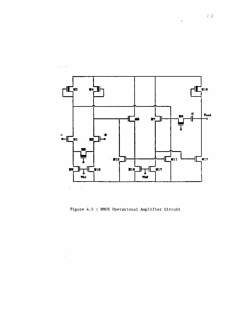
Figure 4.5 : NMOS Operational Amplifier Circuit

Figure 4 . 6 : Comparison of SPICE2 and SPLICE1.6 for NMOS Operational Amplifier Circuit in Fig. 4.5
4.t
2.0
0.0
1 I I
I
I I I
I
I I I I 0.0 1.0 2.0 3.0 4.0
TIME ( p S )

52
5. CONCLUSIONS
SPLICE1.6 has been greatly improved by incorporating the new tech-
niques described in this report. As evidenced by the statistics in Chap. 4, the
new electrical simulation approach, ITA, is substantially faster than SPICE2
and requires f a r less storage. This method has shown so much promise that
efforts are underway to generalize it as a standard circuit simulation
approach. As pointed out earlier, the major problem with the method is the
number of iterations required to obtain a solution when Boating capacitors
are present in the circuit. As the prototype program is developed further, it
is expected that the the performance characteristics will be significantly
better than SPICE2 The ITA method provides a way to efiiciently simulate
large digital circuits and it may replace the standard approach in this appli-
cation. I t is also suitable for implementation on special-purpose hardware
and work is underw3.y in this area.
The logic analysis in SPLICE1.6 has been enhanced to perform true-value
logic simulation using a strength-oriented MOS model. This not only allows
accurate modeling at the logic level but also provides a mechanism to per-
form accurate mixed-mode simulation. There is still work to be done in the
area of strength modeling for logic elements so that the electrical/logic
interfaces can be defined accurately. SPLJCE1.6 handles logic transfer gates
in a consistent manner but there are still unanswered questions in the area
of delay modeling a t the switch-level. Research is currently being directed
at applying multiple iterations at the logic level to determine delays.
53
In conclusion, the concepts presented in this report suggest that
mixed-mode electrical and logic simulation is best applied at the transistor-
level using relaxation-based algorithms and event-driven selective trace
techniques, along with consistent signal representation for accurate conver-
sions from one domain to the other.

54
References
1.
2.
3.
4.
5.
8.
7.
6.
9.
10.
A.R. Newton, The Sarndation of Large Scale In tegrated Circui ts , Univer-
sity of California, Berkeley (July 1976). Ph.D. Dissertation
A.R. Newton, “The simulation of large scale integrated circuits,” IEEE
l”runs. o n E r c c i t s u n d S y s t e m s Vol. CAS-26pp. 741-7453 (September
1979).
A.R. Newton, “Timing, Logic and Mixed-mode Simulation for Large MOS
Integrated Circuits.” pp. 175-240 in Computer Design Aids for GT-
cuits, ed. P. Antognetti, D.O. Pederson, and H. De Man,Sijithoff and
Noordhoff (1981).
B.R. Chawla, H.K. Gumrnel , and P. Kozak, “MOTIS-an MOS timing simula-
tor,” IEEE Dam. on CASVol. CAS-22 pp. 901-909 (Dec. 1375).
S.P. Fan, M.Y. Hsueh, A.R. Newton , and D.O. Pederson, “MOTIS-C A new
circuit simulator for MOS LSI circuits,” Proc. IEEE I n t . Symp o n Cir.
and Syst. , (April 1977).
ur w---i “CDTPFQ A cc-....t ..- D.-..---- 4- ,;-..int-, ,-n-;nnn~.3-tn.- c;c- 1 1 . , . L A g b L , -1 IVYL-, I I I > r y U L L ’ 1 I “&‘U.ll *” Jl , l l .A,Urr d c I I . . L . Y , I L L I ~ - r ” ” I .I
cuits,” ERL-M520, University of California, Berkeley, California (May
1975). Ph.D: Dissertation
LOGIS: User’s Munual Version 4, ISD Corporation (1980).
F. Jenkins, ILOGS: User’s Munual , Simutec (1932).
R.E. Bryant, “An Algorithm for MOS Logic Simulation,” LAMBDA, pp. 46-
53 (4th Quarter 1980).
C.M. Baker and C. Terman, “Tools for Verifying Integrated Circuit
Designs ,” LAMBDA, (4th Quarter 1980).

55
11.
12.
13.
14.
15.
16.
17.
18.
19.
J.L. 3urns, A.R. Newton, and D.O. Pederson, “Active Device Table Look-up
Models For Circuit Simulation,” R o c . 1983 Int. Symp. o n C~TC and Syst . ,
(May 1983). -
A.R. Newton and A.L. Sangiovanni-Vincentelli, Relaxation-Based Electri-
cal Simulation, University of California, Berkeley (1983). To be pub-
lishe d.
“Advanced statistical analysis program (ASTAP) Program reference
manual,” Pub. No. SH20-1118-0, IBM Corp. Data Proc. Div., White Plains,
N-Y
N. Tanabe, H. Nakamura, and K. Kawakita, “An MOS Circuit Simulator for
LSI,” Proc. IEEE Int. Symp. o n Circ. and Syst., pp. 1035-1039 (April
1980).
G.R. Boyle, Simulation o f Integrated Injection Logic, University of Cali-
fornia, Berkeley (March 1978). Ph.D. Dissertation
J.M. Ortega and W.C. Rheinboldt, Iterafive Solution of Nonlinear Equa-
tions in Several Variubles, Academic Press, New York (1970).
K. Sakallah a?d S.W. Director, “An activity-directed circuit simulation
algorithm,” R o c . IEEE Int . Con$ o n ~ T C . and Computers, (October
1980).
E. Cohen, Performance Limits of Integrated Circuit Simulation o n a
Lkdicded Minicomputer System, Bell Laboratories internal memoran-
dum (May 1981).
A. Vladimirescu and D.O. Pederson, “Performance Limits of the CLASSlE
Circuit Simulation Program,” Proceedings of the Int . Symp. o n ETC. and
Syst. , (May 1982).
56
20. E. Lelarasmee, A. Ruheli , and A.L. Sangiovanni Vincentelli, “The
Waveform Relaxation Method for the Time-Domain Analysis of Large
Scale Integrated Circuits,” IEEE Fran. o n CAD of I n t . arc. a n d Sys. Yo1
CAD 1. NO. 3 pp. 131-145 (Aug 82).
21. J. White and A. Sangiovanni-Vincentelli, “RELAX2 A New Waveform
Relaxation Approach for the Analysis .of LSI MOS Circuits,” Proc. 1983
I n t . Symp o n Circ. and S y s t . , (May 1983).
22. J. E. Kleckner, R. k Saleh , and k R. Newton, ‘‘Electrical Consistency in
Schematic Simulation,” Proc. IEEE In t . Con$ o n ETC. and Comp., pp.
30-34 (October 1982).
23. R. A. Saleh, J. E. Kleckner, and A. R. Newton, “Iterated Timing Analysis
and SPLICE1.6,” Proc. IEEE I n t . Conf . o n Compte?--Aided Design, (Sep-
tember 1983).
24. L.0. Chua and P.M. Lin, Compter -A ided Analysis of Electronic Circuits:
ALgorithms & Compitat ional Techniques, Prentice-Hall. Inc., Englewood
Cliffs, N.J. (1970).
25. A.R. Newton, “The Analysis of Floating Capacitors for Timing Simula-
tion.” Proc. 13th Asilomar Conference o n C’ircuits S y s t e m s and C o m p t -
e m , (November 1979).
26. H. Schichman and D.A. Hodges, “Modeling and Simulation of Insulated
Gate Field-Effect Transistor Switching Circuits,” IEEE Journ . o n Solid
S t a t e CLrcuits Vol. Sc-3 pp. 285-289 (Sept. 1968).
27. J.E. Kleckner, I tera ted T iming Andysis and SPLICEZ, To be published
28. G.R. Case, “The SALOGS - A CDC 6600 Program to Simulate Digital Logic
Networks,” Sandia Laboratory Report No. SAND 74-044 (1975).

57
29. D. Dumlugol, H. De hfan , P. Stevens, and G. Schrooten , Local Reluzat ion
Agor i thms f o r Event Driven Simulation of MOS Networks Including
Assignable Delay MadeUing, Katholieke Universiteit Leuven, Belgium ().
To be published.
30. Graeme Boyle, Private communication.
31. Gregory D Jordan and Ravi M. Apte, “Modeling of MOS Transistors in a
Logic Simulator,” Bot. IEEE Int . Conf. o n a r c . and Comp., pp. 431-434
(October 1982).
32. C.J. Terman, Sirnulation Tools f o r Digital LSI Design, Massachusetts
Institute of Technology (December 1981). Proposal for Ph.D. Research
33. , The TTL Data Book, f o r Design Engineers - 2nd Edition, Texas Instru-
ment Incorporated (1976).
34. Jim Kleckner constructed the CDE circuit.
35. D. Senderowicz, An NMOS Integrated Vector-Locked Loop, University of
California, Berkeley (Nov. 1982).


APPEXDMI
SPLlCE1.6 User's Guide


APPENDIXII
SPLICE1.6 Data Structures


spLIcE1.6 Data Structures
1 2 3 4
5
6
(1) Nodes: The node data structure is set up in GENFS for the logic, electrical and wail nodes.
fip type ts+ ival
lstr
modptr
LOGIC NODE :
I
1 7 I dectirn
deflnition fanout pointer fanin pointer =1 (for logic node) =-1 (for logic output node) fanout schedule time logic value (%bits for current value b2blb0 Sbits for previous value b5b4b3
logic strength (ltbbits for current value ltbbits for previous value minimum strength = 1 ; maximum strength = 65,536 1: capacitance at node 2 node decay delay value node decay time
1=0,2=1,3=X)
ELEXT€UCAL NODE :
VRAILNODE: .
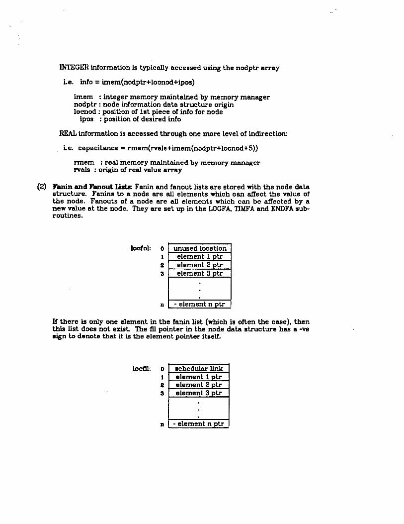
IN”ZGE% information is typically accessed using the nodptr array
Le. info = imem(nodptr+locnod+ipos)
h e m : integer memory maintained by memory manager nodptr : node information data structure origin locnod : position of 1st piece of info for node
ipos : position of desired info
REAL information is accessed through one more level of indirection:
, Le. capacitance = rmem(rvals+imem(nodptr+locnod+5))
rmem : real memory maintained by memory manager rvals : origin of real value array
(2) Panin and F’anout Zists: Fanin and fanout lists are stored with the node data structure. Fanins to a node are all elements which can afIect the value of the node. Fanouts of a node are all elements which can be af€ected by a new value a t the node. They are set up in the LOGFA. TIMFA and ENDFA sub routines.
n B elementn tr
If there is only one element in the fanin list (which is often the case), then this list does not exist. The fll pointer in the node data structure has a -ye sign to denote that it is the element pointer itself.

(3) Yodels: SPLICE1 stores model information using two levels of indirection so that one model may be referenced by many elements.
model info pointers are stored in an array called mdmptr:
z lB locmod2
x i 3m locmodn
locmod points into a table called modptr which is organized as follows:
modptr: E lot ar 1
I
(model type) (location of parameters)
locpar points into nrals which is an array of floating-point quantities and so parameters are accessed as follows:
parameter = rmem ( rvals + locpar)
The rvals array is just a set of real values in the rmem space.
d s :
o H rvalue n
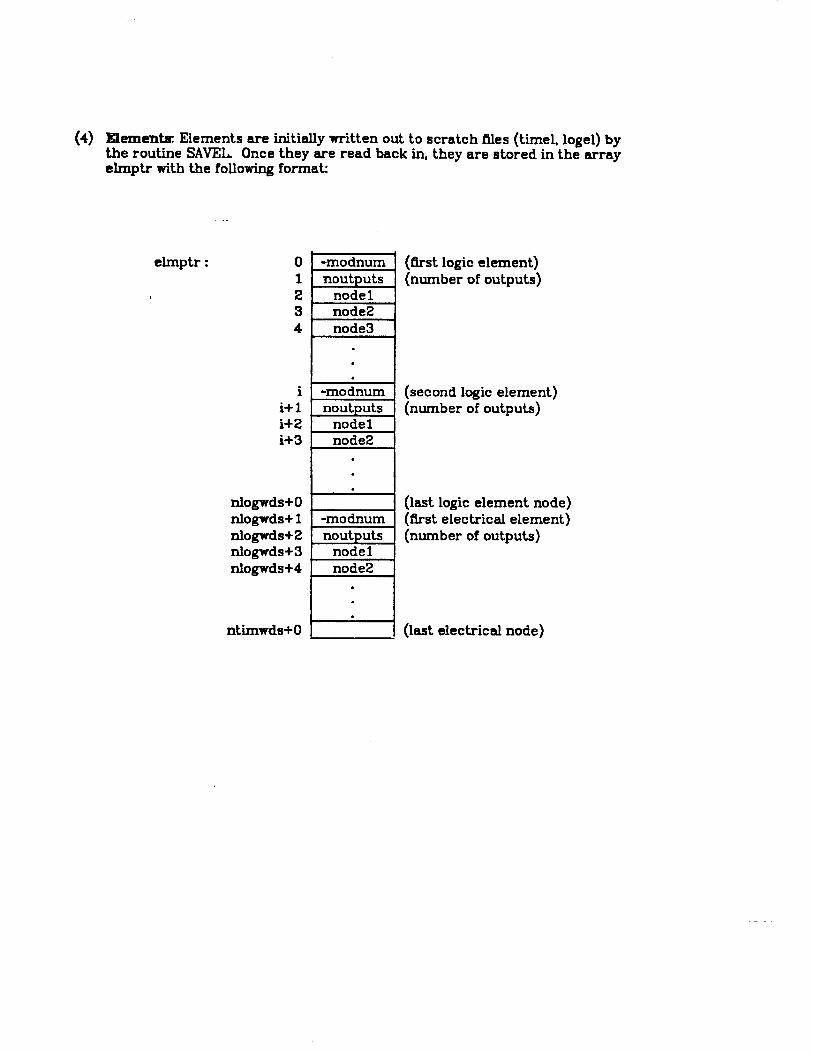
(4) Elements Elements are initially written out to scratch files (timel, logel) by the routine SAVEL Once they are read back in, they are stored in the array elmptr with the following format:
2 3 4
elmptr :
nodel node2 node3
1 nout uts
i i+ 1 i+2 i+3
-modnum
nodel node2
nlogwds+o nlogwds+ 1 nlogwds+2 nlogwds+3 dogwdS+4
ntimwds+O I I
(first logic element) l (number of outputs)
(second logic element) (number of outputs)
(last logic element node) (first electrical element) (number of outputs)
(last electrical node)

(5) Schedular: The time queue is made up of 2 - 100 word arrays and a pool for any events which do not fall within 200 timepoints of the beginning of the queue.
UEUE1 time 0 1 2
lscbl : 99
-
iscb2 :
hcb2 :
iscb3 :
lscb3 :
LOCFOL 1 TIME 2
LOCFOL 2
LOCFOL 3


APPENDM III
SPLlC51.6 Qectrical ELement Model Equatiaas _- _.


Qectrical Qement Yodel Equations
2. Floating Capacitors
b. Saturation Region

Drain Node