embedded capacitance – planar...
TRANSCRIPT

Embedded CapacitorsPresented by John Andresakis
VP of Strategic TechnologyOak-Mitsui Technologies
11-05

AgendaOverview of Embedded Capacitance
Materials
Product Design
PWB Manufacturing Process
Testing
Selection Process
Summary
Embedded capacitor
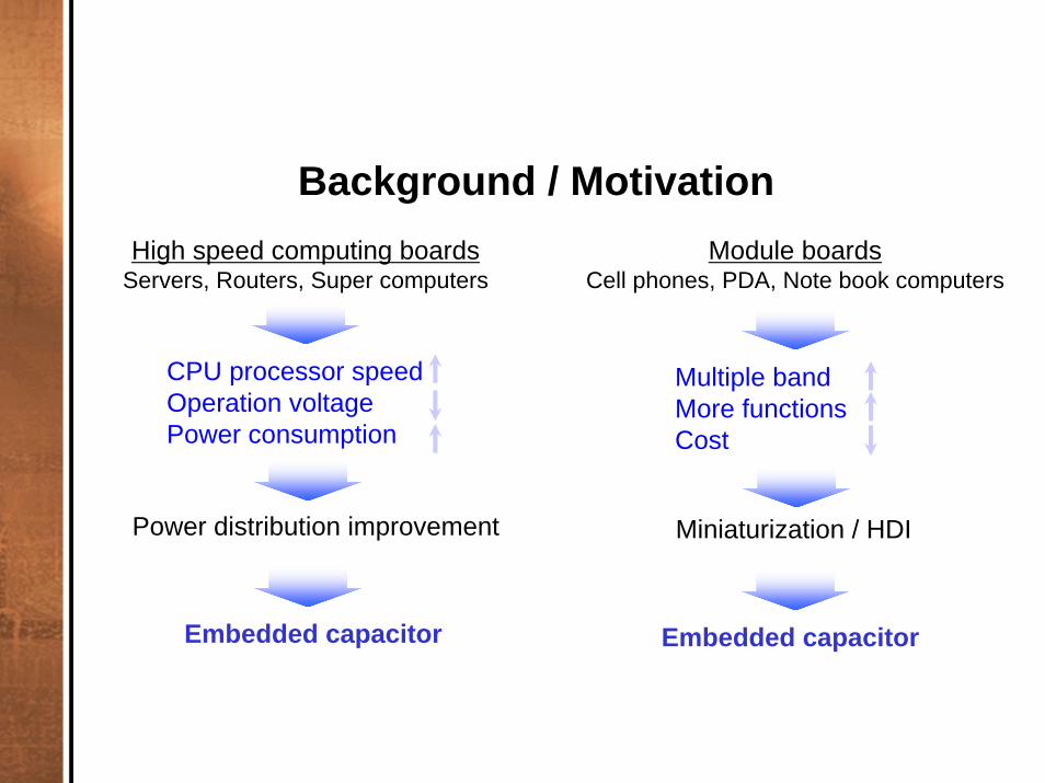
High speed computing boardsServers, Routers, Super computers
Module boardsCell phones, PDA, Note book computers
CPU processor speedOperation voltagePower consumption
Power distribution improvement
Multiple bandMore functionsCost
Miniaturization / HDI
Background / Motivation
Embedded capacitor

Background of demand for PCB with Embedded Capacitor
V
⊿V=I*R+L*di/dt
Voltage Regulator
PowerGround
ICEmbedded
capacitance layer
0.5 1.0 1.5 2.0 2.5 3.0 3.5 4.0 4.5 5.0
Itanium
ITRS 2010
AthalonPentium 1
486386
VoltageP
ower
(W)
Voltage is decreasing
TimeAllowable ⊿V is ±5% of Voltage
⊿V
Will increase as Power increase
Will increase as clock speed increase
50
100
150
ITRS, Swaminathan etal.
⊿V<50mV
⊿V<250mV⊿V<500mV
“Thin” power ground plane is the key parameter to improve electrical performance at high frequency!

Background of demand for PCB with Embedded Capacitor
Component density is reaching its limit
Passive components
Source: Richard Ulrich University of Arkansas
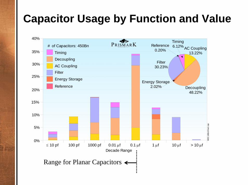
Capacitor Usage by Function and Value
Range for Planar Capacitors
30%
25%
40%
20%
35%
15%
10%
5%
0%
Timing6.12%
Filter30.23%
AC Coupling13.22%
Decoupling48.22%
Energy Storage2.02%
Reference0.20%
# of Capacitors: 450Bn
Timing
Decoupling
AC Coupling
Energy Storage
Reference
Filter
Decade Range
M32
.148
rd-fi
nal c
ap
10 pf≤ 100 pf 1000 pf 0.01 fµ 0.1 fµ 1 fµ 10 fµ > 10 fµ

They Can be Really Small!
0402 resistor:– (It’s the same size as
President Lincoln’s bow tie)
Now find the 0201 capacitor:
Now inspect 2000 parts like this on one board
Is there really such a thing asan 01005?:
-Concern over Placement, Tombstoning, etc.-Still need Vias for connecting
Courtesy of R. Snogren
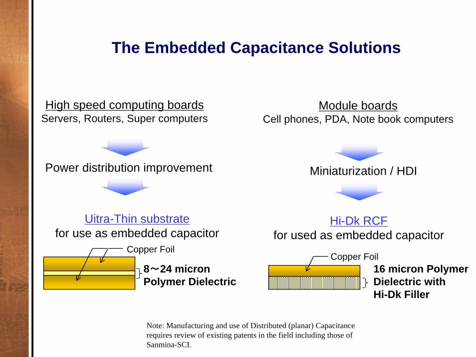
The Embedded Capacitance Solutions
High speed computing boardsServers, Routers, Super computers
Module boardsCell phones, PDA, Note book computers
Power distribution improvement Miniaturization / HDI
8~24 micron Polymer Dielectric
Uitra-Thin substratefor use as embedded capacitor
Copper Foil
Hi-Dk RCF for used as embedded capacitor
16 micron PolymerDielectric with Hi-Dk Filler
Copper Foil
Note: Manufacturing and use of Distributed (planar) Capacitance requires review of existing patents in the field including those of Sanmina-SCI.
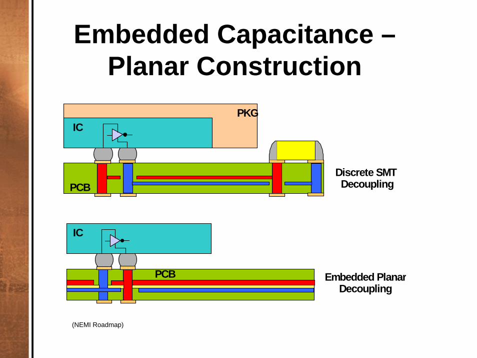
Embedded Capacitance –Planar Construction
IC
PCB
ICPKG
PCB
Embedded PlanarDecoupling
Discrete SMT Decoupling
(NEMI Roadmap)

Planar CapacitanceParallel planes – a very simple idea
A*Dk*Kt
C =
At
PowerDielectricGround
Where:
C = Capacitance (Farads)
A = Area of plates
Dk = Dielectric constant of material between plates
K = Constant
t = Thickness between plates

Planar Capacitor Materials

Ultra-Thin Substratesfor use as
Power Distribution Layers
Construction of ultra-thin substrate
Copper Foil
Copper Foil
Dielectric layer8 to 24 um

Planar CapacitanceMaterial Sets
Capacitance layers (power and ground)Thin Organic dielectrics
Epoxy-fiber glass (FR-4)Modified Epoxy Film Epoxy filled with BaTiO3
Polyimide FilmPolyimide filled with BaTiO3
Proprietary resinsThin Inorganic dielectrics
ParaelectricsFerroelectrics
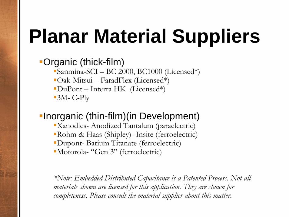
Planar Material SuppliersOrganic (thick-film)
Sanmina-SCI – BC 2000, BC1000 (Licensed*)Oak-Mitsui – FaradFlex (Licensed*)DuPont – Interra HK (Licensed*)3M- C-Ply
Inorganic (thin-film)(in Development)Xanodics- Anodized Tantalum (paraelectric)Rohm & Haas (Shipley)- Insite (ferroelectric)Dupont- Barium Titanate (ferroelectric)Motorola- “Gen 3” (ferroelectric)
*Note: Embedded Distributed Capacitance is a Patented Process. Not all materials shown are licensed for this application. They are shown for completeness. Please consult the material supplier about this matter.

Sanmina-SCI(BC 2000™)
Benchmark for Embedded Planar CapacitanceMaterial supplied by most major LaminatorsCapacitance density 506pF/in2 [78 pF/cm2]High Tg (170C) epoxy resin with106 fiberglass Thin dielectric (0.002” [50 µm]) Hi-Pot testing voltage 500 VDC 0.5, 1 or 2 oz Cu foil (Double treat or Reverse Treat Foil)Patent Portfolio around the Materials and Use of Embedded Planar Capacitance
Example: 1 layer pair on a 16”X20” board will produce about 146 nF;7 layer pairs will approach the mF range.
Note: BC2000 is a trademark of HSCI (Sanmina-SCI Corp)

Oak-Mitsui(FaradFlex®)
BC 8,12,16,24Modified Epoxy Film dielectric Dk 4.4Hi-pot tested to 500 VDCCapacitance Density up to 480 pF/cm2
BC12TM, BC16TFilled (with High Dk particles) Modified Epoxy Film DielectricBC12TM- Dk 10, BC16T- Dk 30Hi-pot Tested to 500 VDC for BC12TM, 100 VDC for BC16TCapacitance Density up to 1700 pF/cm2

Oak-Mitsui Embedded Capacitor Material Characteristics
NA=Not Applicable
PropertiesMethod
IPC or others BC24 BC16 BC12 BC8 BC12TM BC16T
Dielectric Thickness, µm Nominal 24 16 12 8 12 16Cp@ 1MHz, nF/in2(pF/cm2) IPC TM-50
2.5.5.3 1.0 (155) 1.6 (250) 1.9 (300) 3.1 (480) 4.5 (700)
Dk @1Mhz IPC TM-50 2.5.5.3 4.4 4.4 4.4 4.4 10 30
Loss Tangent @ 1 MHz IPC TM-50 2.5.5.3 0.015 0.015 0.015 0.016 0.019 0.019
Peel Strength, lbs/in IPC TM-50 2.4.9 >8 >8 >8 >8 >4 >6
Dielectric Strength, kV/mil IPC TM-50 2.5.6.3 5.3 7.3 5 5 6.2 2.8
Tensile Strength, Mpa (kpsi) ASTMD-882A 152(22.0) 164(23.8) 194(28.2) 126(18.3) 110(16.0) NA
Elongation, % ASTMD-882A 18.5 16.5 11.5 8.5 6.0 NA
CTE, ppm/oCx-y d(20-100oC)/ (100-200oC)
TMA 14 / 23 14 / 23 14 / 23 16 / 28 16 / 38 NABoil test, 2hrs Boil in water, 20
sec dip @260C solder (10spec)- Pass Pass Pass Pass Pass Pass
Thermal Stress (20Sec Float @288C), Times >10 >10 >10 >10 >10 >10
Migration, 85C/85%RH/DC 35V - >1000 >1000 >1000 >1000 >1000 >1000Flammability/Temp Rating UL-94/
UL746V0
130oCV0
130oCV0
130oCV0
PendingV0
130oC
PWB Processing Both side etching
Sequential Lamination
11 (1700)
-
-
Both side etching
Both side etching
Both side etching
Both side etching
V0130oC

Oak-Mitsui Embedded Planar Capacitor Example
Server Board
Capacitor Core 12 µm
24 Layer Board
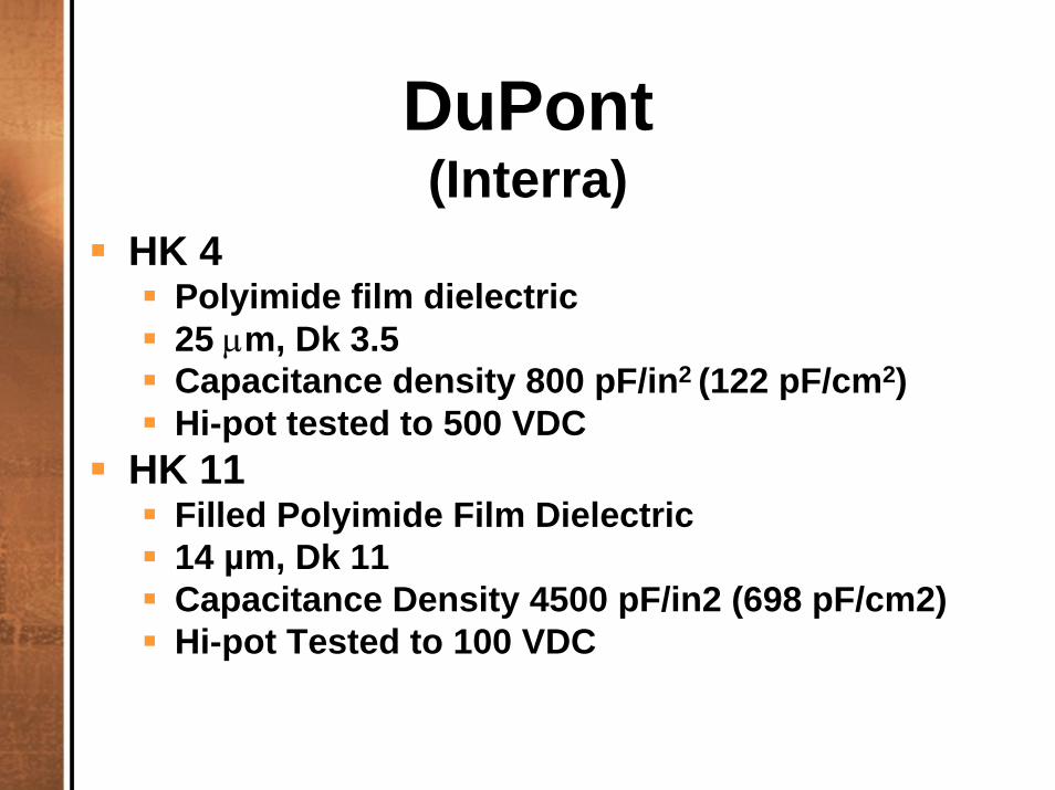
DuPont(Interra)
HK 4Polyimide film dielectric 25 µm, Dk 3.5Capacitance density 800 pF/in2 (122 pF/cm2)Hi-pot tested to 500 VDC
HK 11Filled Polyimide Film Dielectric14 µm, Dk 11Capacitance Density 4500 pF/in2 (698 pF/cm2)Hi-pot Tested to 100 VDC

DuPont HK4
25µ HK4

3M(C-Ply)
Epoxy dielectric filled with BaTiO3Un-reinforced 0.16 to 1 mil [4 to 25 µm] thick (16 µm in
commercialization)Clad with 1oz copper (other weights
available)Capacitance range:
5 to 30 nF/in2 [0.78 to 4.65 nF/cm2]Dk 15 – 23 (16 µm in commercialization)Hi-pot tested to 100 VDC

3M C-PLY
Pair of C-Ply cores on a sub-composite
Adjacent C-Ply cores
Single C-Ply core
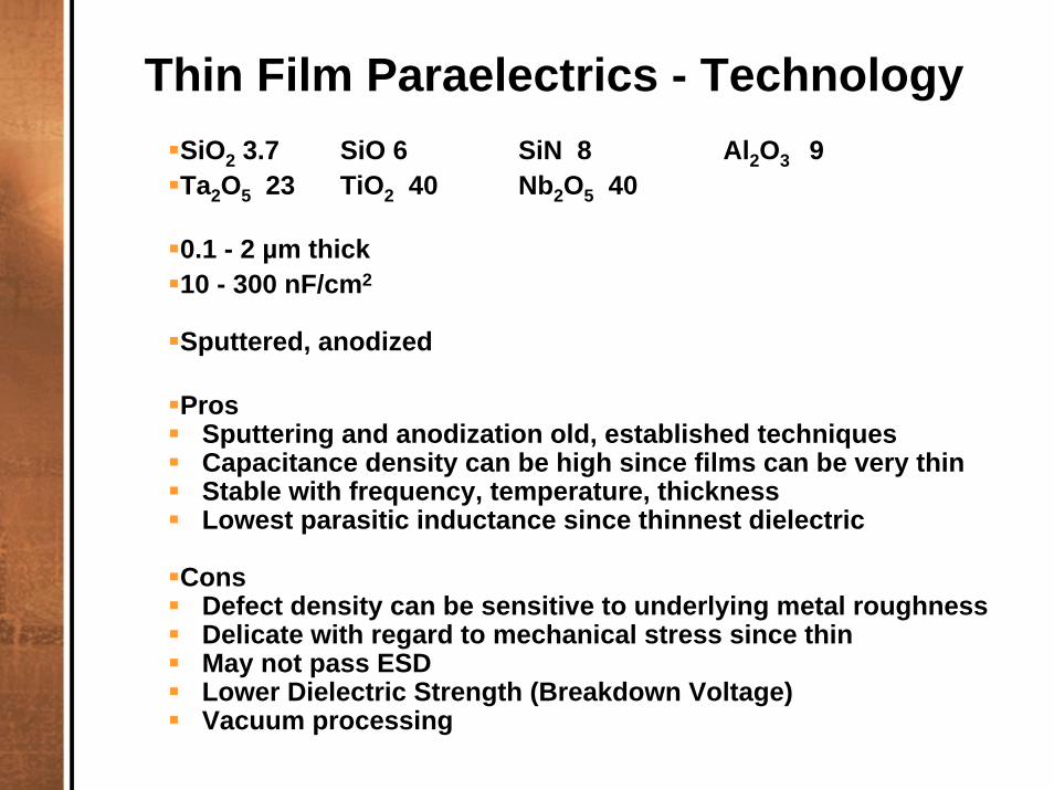
Thin Film Paraelectrics - TechnologySiO2 3.7 SiO 6 SiN 8 Al2O3 9Ta2O5 23 TiO2 40 Nb2O5 40
0.1 - 2 µm thick10 - 300 nF/cm2
Sputtered, anodized
ProsSputtering and anodization old, established techniquesCapacitance density can be high since films can be very thinStable with frequency, temperature, thicknessLowest parasitic inductance since thinnest dielectric
ConsDefect density can be sensitive to underlying metal roughnessDelicate with regard to mechanical stress since thinMay not pass ESD Lower Dielectric Strength (Breakdown Voltage) Vacuum processing

Thin Film Thin Film ParaelectricsParaelectrics - Products
Rohm & Haas (Shipley) - InSiteTM
SiOx10 - 15 nF/cm2
Xanodics - StealthTM Capacitoranodized Ta2O5k = 23, 1000 Å, 200 nF/cm2

Ferroelectrics - Technologyk = 1000 to 20,0001 - 10 µm100 - 2000 nF/cm2
Barium Titanate, Barium Strontium Titanate, Lead Zirconate Titanate, etc
Sputtered, sol-gel, CVD, MOCVD or thick film precursorCured at >600°C in oxygen
ProsCapacitance density can be very highParasitic inductance can be low since thin dielectric
Cons Requires >600°C cure, not directly processible on organic
substratesCan be expensiveCapacitance varies with T, frequency, voltage, thickness

FerroelectricsFerroelectrics - Products
DuPont - InterraTM
BaTiO3 Thin Film on CopperUnder Development
Rohm &Haas with Energenius - InSiteTM
“S3” Under developmentPZT sol-gel200 nF/cm2 reported
Motorola“Gen 3”PZT sol-gelUnder Development
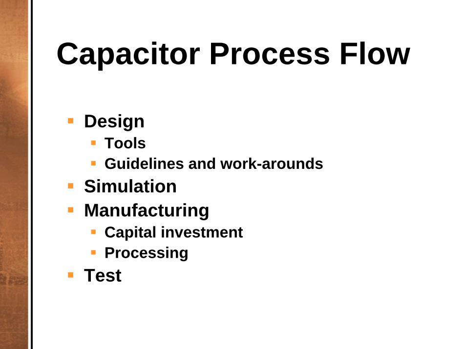
Capacitor Process Flow
DesignToolsGuidelines and work-arounds
SimulationManufacturing
Capital investment Processing
Test

Designing Capacitors
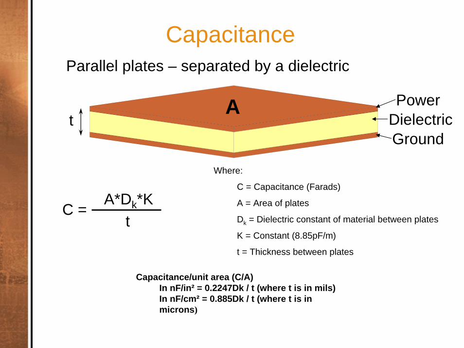
CapacitanceParallel plates – separated by a dielectric
A*Dk*Kt
C =
At
PowerDielectricGround
Where:
C = Capacitance (Farads)
A = Area of plates
Dk = Dielectric constant of material between plates
K = Constant (8.85pF/m)
t = Thickness between plates
Capacitance/unit area (C/A)In nF/in² = 0.2247Dk / t (where t is in mils)In nF/cm² = 0.885Dk / t (where t is in microns)

P & G Plane Layer PairMeasure total overall (common/overlapping) copper plane area Subtract the sum of the areas of all via clearances, cut outs and any non copper featuresThe result is the total conductor area or the total effective electrode area of the capacitorMultiply the above area by the capacitance density Be sure to use the same units of area measurementIf more capacitance is required, more planes may be used and/or added specifically for capacitance
IMPORTANT NOTE: Due to decreased inductance the total capacitance needed with embedded capacitors is usually
significantly less then when using discrete capacitors.

Planar CapacitorsAssumptions
Parallel plate, single layer capacitorsDielectric thickness and Dk are constant for a given materialSizing calculations are based on material supplier reported capacitance densityTermination and clearance based on PWB manufacturers registration guidelinesCapacitance tolerances based on material supplier reported capacitance density variance and PWB manufacturers etch tolerance

Design ImpactCapacitor removal
Rules need to be developed for specific system and processor speed
Many tests have been run showing that small value (fast response) decoupling capacitors can be entirely removed with ultrathin materials.
Plane ClearancesUltrathin low Dk materials
The plane clearances need to be strongly consideredMaking cross board plane splits in a line, can create folding issueLarge clearances in both sides of material (ex. high voltage board areas) are to minimized. Hurts handling, increases damage chances, and may hurt registration

Design Impact
Plane clearancesUltrathin High Dk materials
Special processes used on this material make it less susceptible to plane clearance design approaches.
Use in power distributionCarefully select material when using high voltages
Insure adequate breakdown voltage and Hi-Pot survivabilityFilled materials are designed for low voltage applications

Design ImpactUse with high speed circuits
These materials are intended for high capacitance, not controlled impedance or low loss.
Most of the materials have good electrical properties, but not all.
Impedance control across these materials would be reducedConductor loss would be increasedUse of these materials for P/G planes reduces/eliminates this issues
High Dk materials would have negative impact on propagation velocitySome materials are lossy, which is good for noise reduction, but very poor for transmission lines.

Power/Ground Plane Simulation
• Utilize EMI Stream– Developed by NEC– Based on SPICE Model
• Input PCB Layout in Design Format (.dsn file)– Output provide by standard design tools (Mentor
Graphics, Cadence, etc.)• Select thickness, Dk and Cu thickness of P/G
planes• Select frequency range• Can add/subtract discrete SMT capacitors• Other Software Available (ex. Sigrity)

Resonance Distribution
Simulations provided by TechDream, Inc
35- 0.1µF capsfor power supply
+44-0.1 µF capsfor resonances
0.4mm (16 mil P/G)
35- 0.1µF capsfor power supply
Can not place caps!
24 µm P/GDk 4.4No additional caps

Resonance Distribution- Lower Noise Threshold
400 µm (16 mil P/G)79 caps
24 µm P/GDk 4.435 caps
12 µm P/GDk 1035 caps

Frequency Response- Effect of Thickness, Dk
Dk-4.4 Dk-4.4
Dk-30
Dk-10

Process Flow for Embedded Distributed Capacitance
• Select PCB Design as Candidate– Known problem with P/G noise, EMI– High pF Capacitor density
• Provide .dsn file for Simulation• Set-up and run Simulation• Build Prototype based on Simulation• Analyze Prototype and Finalize
design

Manufacturing Processes
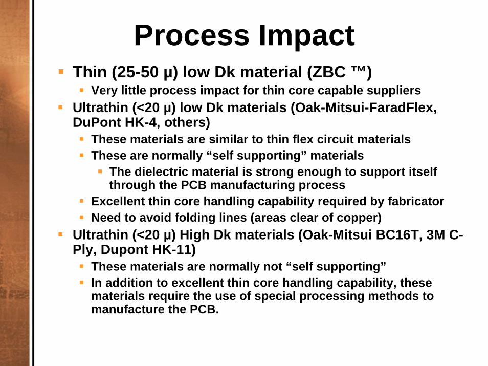
Process ImpactThin (25-50 µ) low Dk material (ZBC ™)
Very little process impact for thin core capable suppliersUltrathin (<20 µ) low Dk materials (Oak-Mitsui-FaradFlex, DuPont HK-4, others)
These materials are similar to thin flex circuit materialsThese are normally “self supporting” materials
The dielectric material is strong enough to support itself through the PCB manufacturing process
Excellent thin core handling capability required by fabricatorNeed to avoid folding lines (areas clear of copper)
Ultrathin (<20 µ) High Dk materials (Oak-Mitsui BC16T, 3M C-Ply, Dupont HK-11)
These materials are normally not “self supporting”In addition to excellent thin core handling capability, these materials require the use of special processing methods to manufacture the PCB.
Processing Guidelines
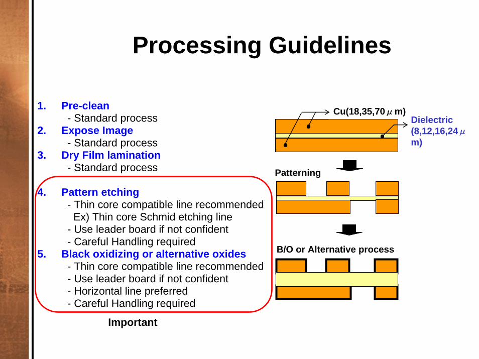
1. Pre-clean- Standard process
2. Expose Image- Standard process
3. Dry Film lamination- Standard process
4. Pattern etching - Thin core compatible line recommended
Ex) Thin core Schmid etching line- Use leader board if not confident - Careful Handling required
5. Black oxidizing or alternative oxides- Thin core compatible line recommended- Use leader board if not confident- Horizontal line preferred- Careful Handling required
Patterning
B/O or Alternative process
Dielectric (8,12,16,24μm)
Cu(18,35,70μm)
Important

Wet Process Equipment
Standard Line
Ultra flex line
Courtesy of Schmid

Handling Guidelines
Hold panel from 2edges Prevent holding panel from sides
Prevent holding panel with one hand

Planar Materials Not Requiring Sequential
Lamination
Typically Unfilled materials
Material becomes a standard core in a MLB structure
Does require scale characterization
Thin Material Processing Equipment Required

Sequential Lamination
MLB Core
Required for Most Filled Product Required for Thin Film Products Two passes through Inner layer Processing

Testing
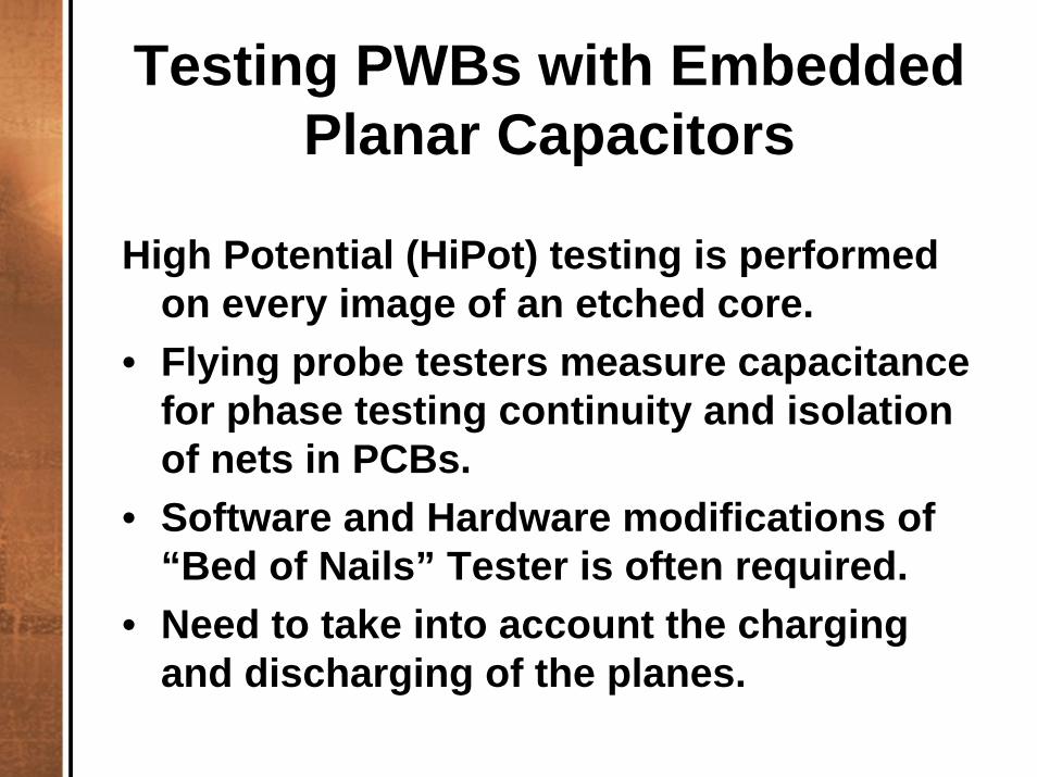
Testing PWBs with Embedded Planar Capacitors
High Potential (HiPot) testing is performed on every image of an etched core.
• Flying probe testers measure capacitance for phase testing continuity and isolation of nets in PCBs.
• Software and Hardware modifications of “Bed of Nails” Tester is often required.
• Need to take into account the charging and discharging of the planes.

-2 .5 -2 -1 .5 -1 -0 .5 0 0 .5 1 1 .5 2 2 .5x 10 ns
-1 .5
-1
-0 .5
0
0 .5
1
1 .5
50 O hm m ode, V =3.3v
TV 1-3-1 B C 2000TV 1-3-1 H i-KTV 1-3-1 E M C A PTV 1-3-1 C -P ly
TV 1-2-1 FR 4+d
(Time Domain - 50 MHz)V
olts
Power Bus Noise (UMR)
Data from NCMS Embedded Decoupling Capacitance Project Report - 12/00
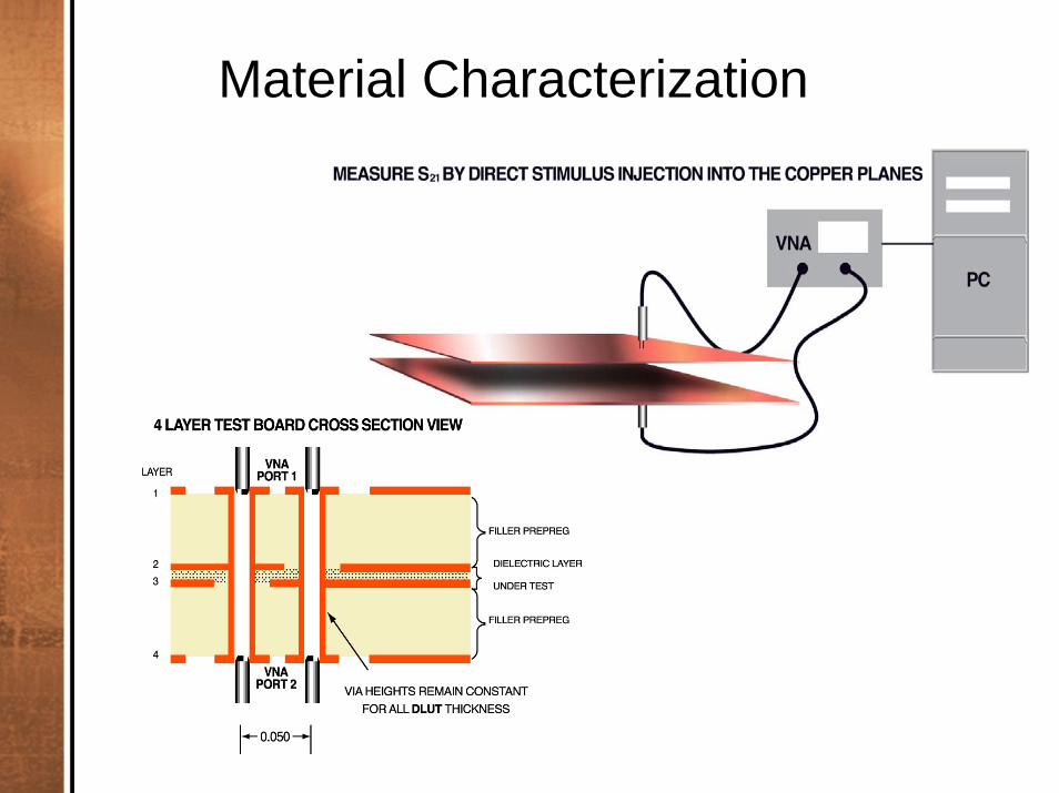
Material Characterization

Power/Ground Self ImpedanceImpedance magnitude [ohm]
1.E-03
1.E-02
1.E-01
1.E+00
1.E+01
1.E+07 1.E+08 1.E+09Frequency [Hz]
50um FR424um C-Ply12um C-Ply 8um C-Ply
Data courtesy of Istvan Novak Sun Microsystems

Transfer ImpedanceImpedance magnitude [ohm]
1.E-03
1.E-02
1.E-01
1.E+00
1.E+01
1.E+07 1.E+08 1.E+09Frequency [Hz]
50um FR424um C-Ply12um C-Ply 8um C-Ply
Data courtesy of Istvan Novak Sun Microsystems
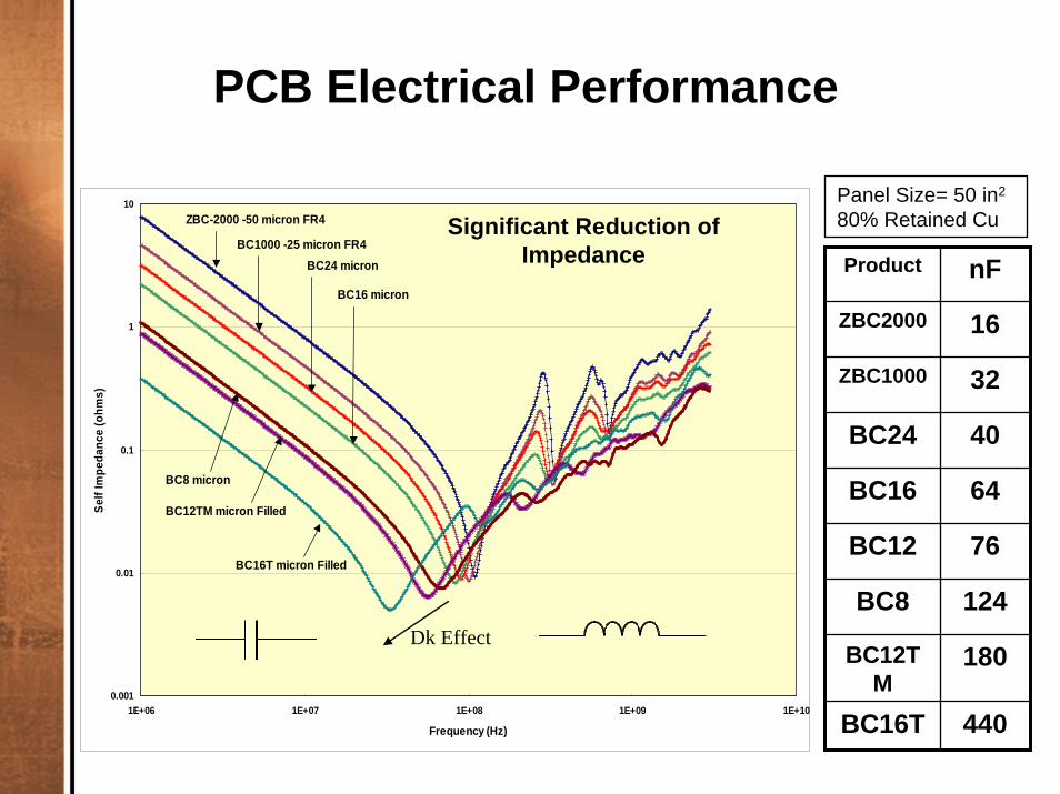
PCB Electrical Performance
Panel Size= 50 in2
80% Retained Cu
0.001
0.01
0.1
1
10
1E+06 1E+07 1E+08 1E+09 1E+10
Frequency (Hz)
Self
Impe
danc
e (o
hms)
ZBC-2000 -50 micron FR4
BC1000 -25 micron FR4BC24 micron
BC16 micron
BC8 micron
BC12TM micron Filled
BC16T micron Filled
Significant Reduction of Impedance Product nF
ZBC2000 16
ZBC1000 32
BC24 40
BC16 64
BC12 76
BC8 124
BC12TM
180
BC16T 440
Dk Effect
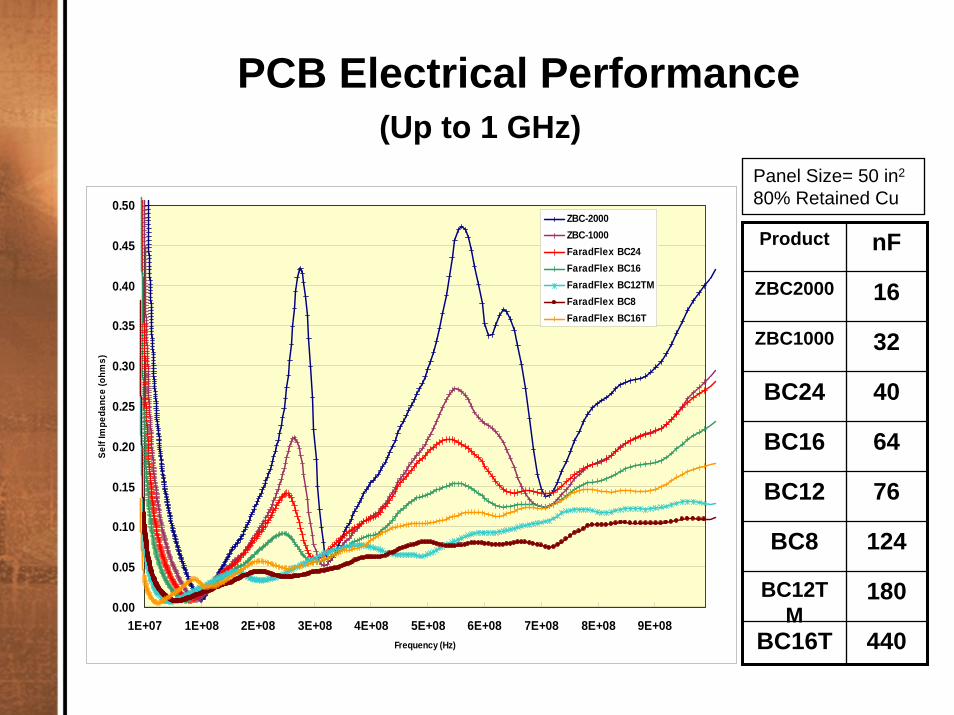
PCB Electrical Performance(Up to 1 GHz)
0.00
0.05
0.10
0.15
0.20
0.25
0.30
0.35
0.40
0.45
0.50
1E+07 1E+08 2E+08 3E+08 4E+08 5E+08 6E+08 7E+08 8E+08 9E+08Frequency (Hz)
Self
Impe
danc
e (o
hms)
ZBC-2000ZBC-1000FaradFlex BC24FaradFlex BC16FaradFlex BC12TMFaradFlex BC8FaradFlex BC16T
Panel Size= 50 in2
80% Retained Cu
Product nF
ZBC2000 16
ZBC1000 32
BC24 40
BC16 64
BC12 76
BC8 124
BC12TM
180
BC16T 440

PCB Electrical Performance(Up to 3 GHz)
0.0
0.1
0.2
0.3
0.4
0.5
0.6
0.7
0.8
0.9
1.0
1.0.E+07 5.1.E+08 1.0.E+09 1.5.E+09 2.0.E+09 2.5.E+09Frequency (Hz)
Self
Impe
danc
e (o
hms)
ZBC-2000ZBC-1000FaradFlex BC24FaradFlex BC16FaradFlex BC12TMFaradFlex BC8FaradFlex BC16T
Product nF
ZBC2000 16
ZBC1000 32
BC24 40
BC16 64
BC12 76
BC8 124
BC12TM
180
BC16T 440
Panel Size= 50 in2
80% Retained Cu
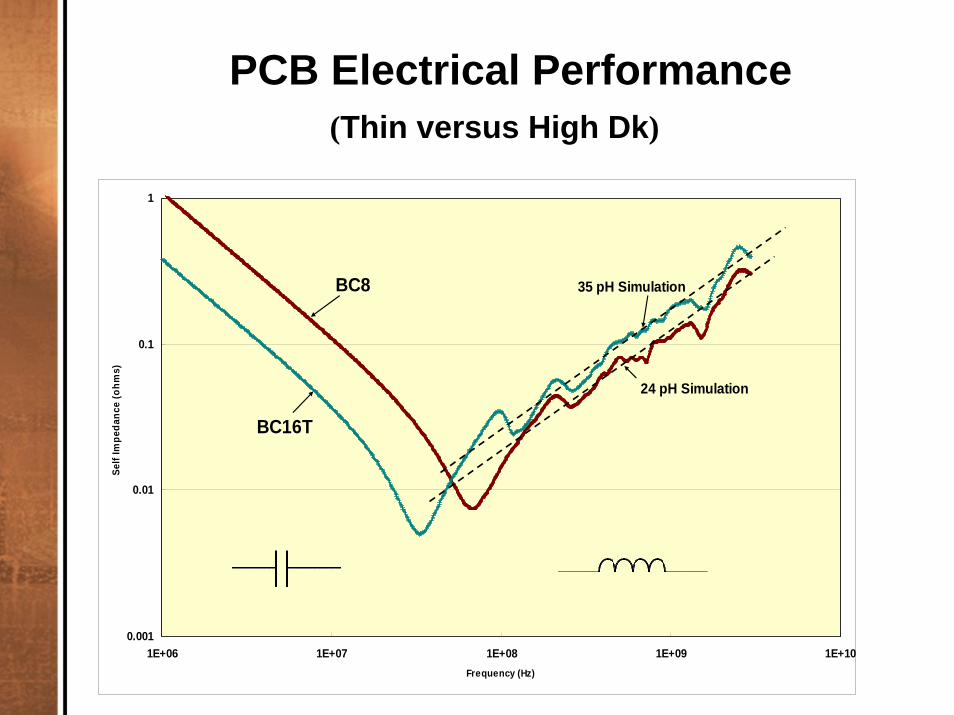
PCB Electrical Performance(Thin versus High Dk)
0.001
0.01
0.1
1
1E+06 1E+07 1E+08 1E+09 1E+10Frequency (Hz)
Self
Impe
danc
e (o
hms)
BC8
BC16T
35 pH Simulation
24 pH Simulation
0.6mm
0.6mm
24 micron core
12 micron core
P.P
P.P
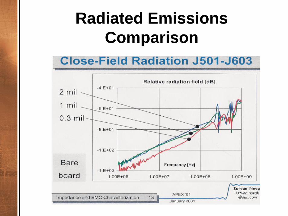
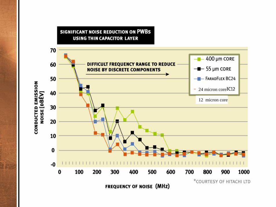
Radiated Emissions Comparison

Success Stories• High Speed Digitial (Multiple Companies)
– Simplified Lay-out– Removed over 800 Caps on one design– Improved Electrical Performance– Improved EMI
• IC Testers (Multiple Companies)– Improved Electrical Performance– Maintained Board Thickness with added layers
• Cable Infrastructure– Removed most caps- able to do single sided assembly– Reduced board size– Maintained board thickness

Discrete Capacitor
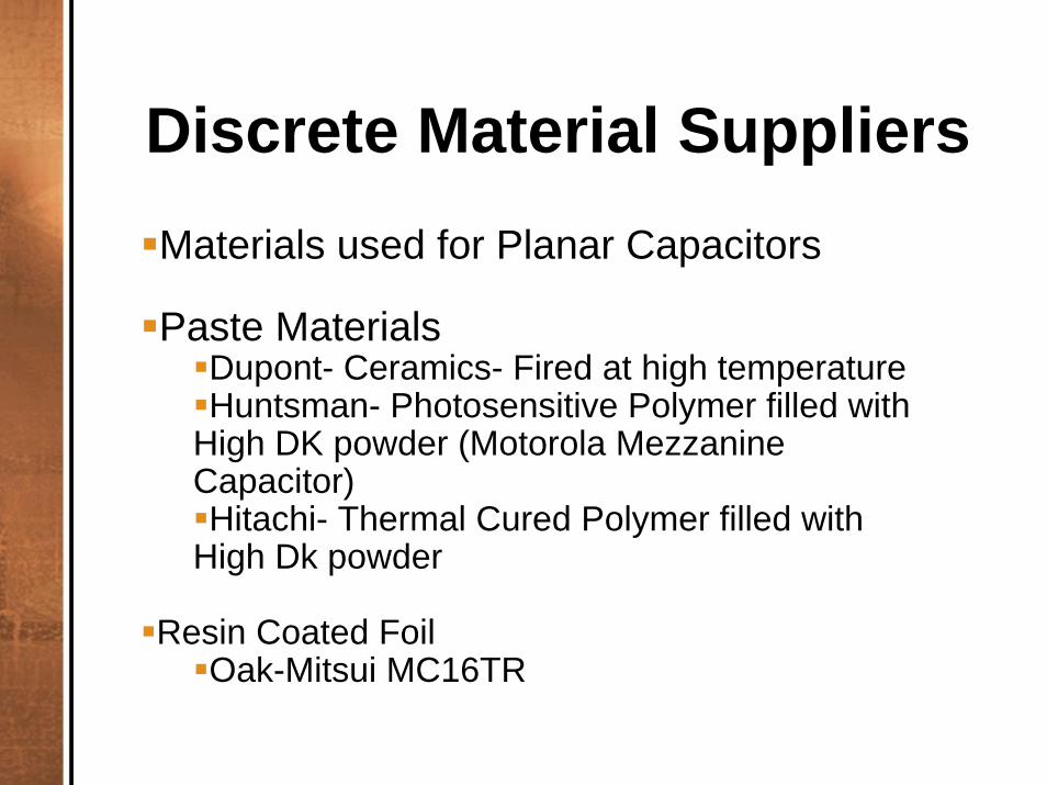
Discrete Material SuppliersMaterials used for Planar Capacitors
Paste MaterialsDupont- Ceramics- Fired at high temperatureHuntsman- Photosensitive Polymer filled with
High DK powder (Motorola Mezzanine Capacitor)Hitachi- Thermal Cured Polymer filled with
High Dk powder
Resin Coated FoilOak-Mitsui MC16TR

Hi-Dk RCF Material Construction
Characteristics Condition Unit BC16TR
Capacitance 1MHz pF/cm2 1,700
Dk 1MHz N/A 30
Df 1MHz N/A 0.019
DielectricThickness Nominal Micron
Meter 16
Thermal Stress 20sec @288C times >10
Peel Strength IPC TM-6502.4.9 kN/m >0.7
Electrical Migration
85C/85%RH/35V hrs >1000
16 micron PolymerDielectric with Hi-DkFiller
Copper Foil

Designing Embedded Capacitance BoardGeometry and Capacitance(Example)
10mm
160pF120pF
80pF
40pF20pF
140pF
60pF30pF19pF
100pF 90pF 70pF
50pF
18pF 17pF 16pF 15pF 14pF 13pF 12pF 11pF 10pF
9pF8pF7pF6pF5pF4pF3pF2pF
1pF - 1.8pF
10mm
40 capacitors ranging from 1pF to 160pF in 10x10mm
Geometry calculated based upon16µ Filled material: 1,700pF/cm2
Expected tolerance*1 - 2pF 5 - 10%2 - 10pF 3 - 5%10 - 20pF 2 - 3% 20 - 100pF 1 -2%100 - < 1%*Based on electrode geometry definition +/- 10micron
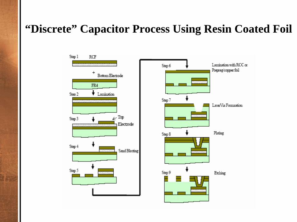
“Discrete” Capacitor Process Using Resin Coated Foil

Removal of dielectric layer
Top view Cross sectional
Before sandblast process
After sandblast process
Top electrode
Dielectric layer
Top electrode
Bottom electrode

Capacitance uniformity evaluation result
0
2
4
6
8
10
12
14
-10 -9 -8 -7 -6 -5 -4 -3 -2 -1 0 1 2 3 4 5 6 7 8 9 10
Deviation from target value(%)
Freq
uenc
y
648m
m
470mm
50.8mm(2inch)
BC16TR
Approx. 44nF
Capacitor size : 50.8x50.8mm192 measurement points Uniformity <5%

Capacitance uniformity evaluation
350mm
21mm
100 capacitors in 1cm2
0.50 x 0.50mm
10mm
10mm
Pattern1
10mm 10mmPattern
2
Pattern 3 Pattern
4
144 module
4 different segment
14,400 capacitor
350mm

Flying Probe LCR measurementof Embedded Passive Boards

Capacitance uniformity evaluation result
0.5 x 0.5mm Capacitor
0
500
1000
1500
2000
2500
3000
-10 -8 -6 -4 -2 0 2 4 6 8 10
Variation from mean value
Freq
uenc
y
Uniformity <7%
3σ=6.7%Mean value: 4.25pF
14,400 capacitor
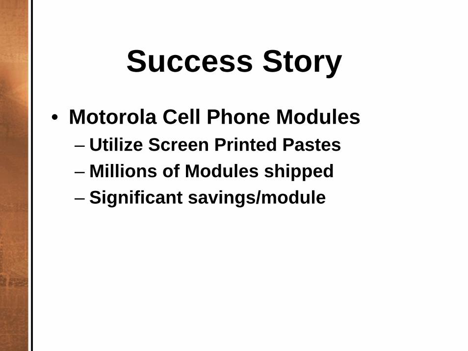
Success Story• Motorola Cell Phone Modules
– Utilize Screen Printed Pastes– Millions of Modules shipped– Significant savings/module

Further Studies
• Measure EMI from assembled boards and compare with Simulation results
• Conduct High Frequency testing on “Discrete” Embedded Capacitors– Test Vehicle Designed– Utilize Crane NAVSEA Facility– Test to 12 GHz

Crane Test Vehicles for High Frequency Testing

Crane Test Vehicles for High Frequency Testing

Selection Criteria
Capacitance Density/InductanceOperating Voltage PWB processes Cost/Performance
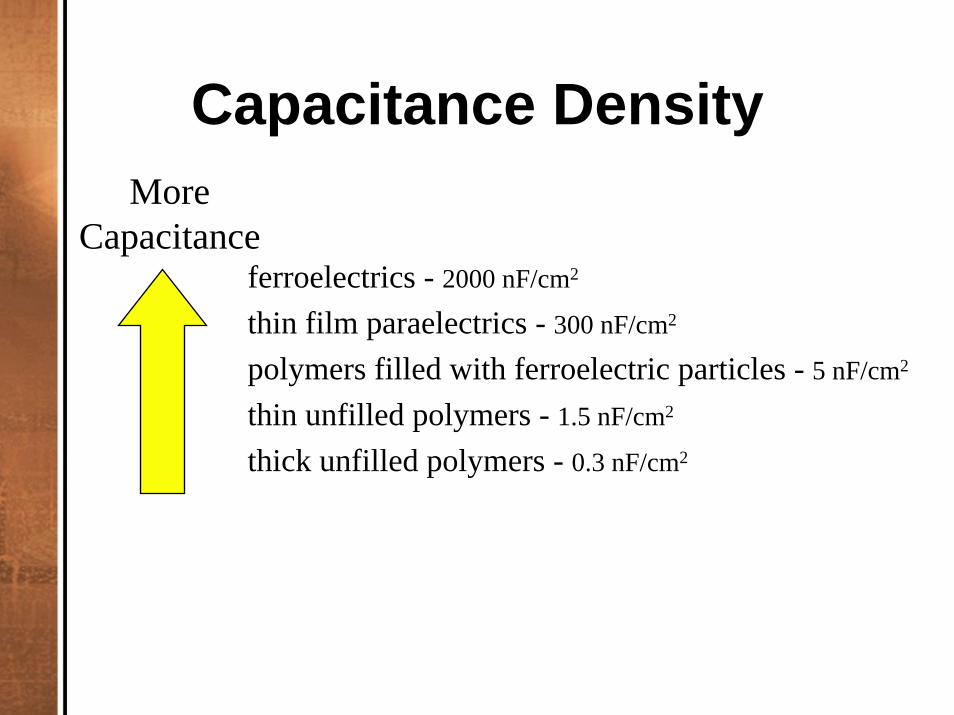
Capacitance Density
ferroelectrics - 2000 nF/cm2
thin film paraelectrics - 300 nF/cm2
polymers filled with ferroelectric particles - 5 nF/cm2
thin unfilled polymers - 1.5 nF/cm2
thick unfilled polymers - 0.3 nF/cm2
MoreCapacitance
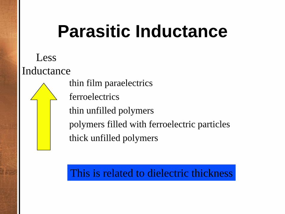
Parasitic Inductance
thin film paraelectricsferroelectricsthin unfilled polymerspolymers filled with ferroelectric particlesthick unfilled polymers
LessInductance
This is related to dielectric thickness

Cost (Roughly) - Per Unit Area
Ferroelectricsthin film paraelectricspolymers filled with ferroelectric particlesthin unfilled polymers thick unfilled polymers
LowerCost

IPC Activities• Standards
– Embedded Capacitor Materials• IPC 4821 Ready for Publishing
– Embedded Resistor Material– Embedded Passive Design– Embedded Passive Performance
• IPC Expo 2006 – Sessions on Embedded Passives
• IPC 3rd Embedded Passives Conference – May 2-4 in Boston Area
• IPC Embedded Devices Users Group– Regular Teleconferences to discuss technology

Summary• Embedded Capacitor Technology can Improve System
Price/Performance by – Reducing Discrete Caps– Reducing PWB size/thickness– Increasing Functionality
• Thinner Power Distribution Planes are required for improved Impedance Performance at high frequency
• New Substrates have demonstrated excellent electrical performance and physical properties.
• They are compatible with PCB processing; a truly “drop in”material.
• Materials are commercially available from Licensed Fabricators
• Substrates Filled with Ferroelectric Particles have better performance, but result in higher cost PCBs

Summary
• Simulation tools exist to help in determine effectiveness of Embedded Capacitors prior to prototyping.
• The use of Embedded Capacitance can simplify PCB lay-out and reduce the number of prototypes required.
• Discrete Capacitors can be formed using High DkResin Coated Foil or Pastes
• Design Tools exists to utilize Embedded Discrete Components
• Research is being conducted on high frequency response of Embedded “Discrete” Capacitors
• Many Success Stories for use of Embedded Passives
