emerging tunnel fet and spintronics based hardware secure
TRANSCRIPT
Emerging Tunnel FET and Spintronics basedHardware Secure Circuit Design with Ultra-lowEnergy ConsumptionAditya Japa ( [email protected] )
Dr Shyama Prasad Mukherjee International Institute of Information Technology https://orcid.org/0000-0003-2408-5400Subhendu K. Sahoo
BITS Pilani: Birla Institute of Technology and ScienceRamesh Vaddi
SRM University AP - AmaravatiManoj Kumar Majumder
Dr Shyama Prasad Mukherjee International Institute of Information Technology
Research Article
Keywords: Tunnel FET (TFET), Differential power analysis (DPA), Sense ampli�er based logic (SABL),Spin transfer torque magnetic tunnel junction (STT-MTJ), Logic-in-memory (LiM), Logicencryption/locking
Posted Date: May 28th, 2021
DOI: https://doi.org/10.21203/rs.3.rs-262353/v1
License: This work is licensed under a Creative Commons Attribution 4.0 International License. Read Full License
Journal of Computational Electronics
Emerging Tunnel FET and Spintronics based Hardware Secure Circuit
Design with Ultra-low Energy Consumption
Aditya Japa · Subhendu K. Sahoo · Ramesh Vaddi · Manoj Kumar Majumder
Abstract
Present CMOS technology with scaled channel lengths exhibited higher energy consumption in designing secure electronic
circuits against hardware vulnerabilities and breaches. Specifically, CMOS sense amplifier based secure differential power
analysis (DPA) countermeasures at scaled channel lengths show large energy consumption with increased vulnerability.
Additionally, spin transfer torque magnetic tunnel junction (STT-MTJ) and CMOS based logic-in-memory (LiM) cells
demonstrate high energy consumption due to the large write current requirement of STT-MTJ and poor MOS device
performance at scaled channel lengths. This paper for the first time leverages emerging tunnel FET (TFET) steep-slope device
characteristics and compatible non-volatile STT-MTJ devices for enhanced hardware security with ultra-low energy
consumption at lower supply voltages. TFET based sense amplifier based logic (SABL) gates have been proposed that achieve
3× lower energy consumption compared to Si FinFET SABL designs. Further, utilizing TFET SABL gates, TFET Pride S-box
is designed that exhibits higher DPA resilience with 3.2× lower energy consumption compared to FinFET designs. With resulted
lower static power consumption, TFET SABL based crypto systems can show lower vulnerability to static power side-channel
attacks. Besides, proposed STT-MTJ and TFET LiM gates achieves 4× lower energy consumption compared to STT-MTJ and
FinFET designs. Moreover, these gates have been explored in logic encryption/locking technique that shows 3.1× lower energy
consumption compared to STT-MTJ and FinFET based design.
Keywords Tunnel FET (TFET) · Differential power analysis (DPA) · Sense amplifier based logic (SABL) · Spin transfer
torque magnetic tunnel junction (STT-MTJ) · Logic-in-memory (LiM) · Logic encryption/locking
1 Introduction
Aditya Japa1
Subhendu K. Sahoo2
Ramesh Vaddi3
Manoj Kumar Majumder1
1Department of Electronics and Communication Engineering,
DSPM International Institute of Information Technology, Naya Raipur 493661, India. 2Department of Electrical and Electronics Engineering, Birla
Institute of Technology and Science, Hyderabad 500078, India.
3Department of Electronics and Communication, School of
Engineering and Applied Sciences, SRM University, Amaravati,
Guntur 522502, Andhra Pradesh, India.
Offshore manufacturing of integrated circuits (ICs) show
increased vulnerability to hardware security attacks in the
modern internet of things (IoT) era [1-2]. In support of this, the
national institute of standards and technology has observed an
exponential growth in hardware vulnerabilities in the last few
years [3]. Moreover, the hardware security aided techniques or
systems market is growing rapidly to avoid the counterfeiting
of ICs [4]. There exist diversified hardware security attacks in
the literature including hardware reverse engineering,
counterfeiting of IC, and side-channel analysis (SCA). Among
different hardware security attacks available, the SCA is
effective in recovering the hidden secret information [5]. SCA
utilizes the side-channel signals like power consumption,
electromagnetic and photonic signals to reveal encryption key
of the cryptographic circuits/systems [6]. Differential power
analysis (DPA) process the power consumption information of
encryption engine and require comparatively less effort in
recovering secret key information [7]. Additionally, static
CMOS logic style shows higher vulnerability to DPA attacks
due to the data dependent power consumption profile [8-9]. To
avoid this, several researchers explored novel logic styles that
show higher DPA resilience [10]. Sense amplifier based logic

Journal of Computational Electronics
(SABL), FinFET based secure adiabatic logic (FinSAL),
randomized multi-topology logic (RMTL), homogeneous
dual-rail logic (HDRL), secure positive feedback adiabatic
logic, and differential symmetric pull-down network gates
have been demonstrated to mitigate the data dependency
on device power consumption [11-16]. Among the novel
logic designs, SABL logic style is proved to be secure and
show several challenges including higher power and
energy consumption overheads [11]. Moreover, at sub-
50nm channel lengths, CMOS SABL exhibited higher
static power consumption that revealed the confidential
information against static power SCA [17]. To avoid this,
emerging hyperFET devices have been leveraged for DPA
resilient SABL logic. However, this technique has
exhibited relatively 3× higher energy consumption
compared to CMOS [18]. Thus, CMOS SABL logic
shown unavoidable disadvantages that need to be
addressed for DPA resilient crypto graphic circuits with
ultra-low energy consumption.
On the other hand, spin transfer torque based magnetic
tunnel junction (STT-MTJ) has attracted wide attention
due to their lower static power, non-volatility and higher
compatibility with CMOS technology [19-20]. Moreover,
integrating STT-MTJ and CMOS provided flexibility to
build logic-in-memory (LiM) architectures for high speed
data transfer [21]. Several researchers demonstrated logic
gates and arithmetic circuits by exploring STT-MTJ based
LiM cells [22-23]. However, STT-MTJ require relatively
large write current to change the state that demands to
maintain higher supply voltages [24]. Besides, CMOS
technology scaling lead to serious problems including
lower ON current, short channel effects, high power
density, and unreliability [25]. Consequently, the STT-
MTJ based LiM circuits exhibited large energy
consumption due to the poor performance of MOS devices
at scaled channel lengths (or supply voltages). In support
of this, recent STT-MTJ LiM cells based crypto circuits
exhibited increased energy consumption [26].
In the recent past, emerging tunnel FET (TFET) with its
band-to-band tunnelling mechanism exhibited steep-slope
characteristics (lower subthreshold swing) and higher ON
to OFF current ratio (ION/IOFF) [27-29]. As a result, TFET
based digital, analog and mixed signal circuits/systems
achieved higher energy efficiency at lower supply
voltages [30-31]. Apart from the low energy consumption
and higher speed benefits, TFET devices with the special
characteristics have been leveraged to enhance hardware
security [32]. TFET based current mode logic and
adiabatic logic have been proposed for differential power
analysis resistant crypto systems [33-34]. TFET based
compact polymorphic logic gates were designed by
exploring the onset of tunnelling for both positive and
negative gate bias [35]. The p-i-n forward current of TFET
is explored as favourable feature to design true random
number generator and low area overhead DPA
countermeasure [36-37]. Thus, at scaled supply voltages,
emerging TFET device has utilized to enhance hardware
security of electronic systems [38]. Therefore, this work
leverages TFET device characteristics for hardware security
techniques that exhibit lower energy consumption. The SABL
logic gates have been designed by exploring TFET device to
reduce the energy consumption. The proposed TFET SABL
gates are applied to design PRIDE S-box. Further, DPA attack
is performed on proposed TFET SABL based S-box and also
the performance is benchmarked with the base line Si FinFET
designs. Additionally, STT-MTJ and TFET based LiM gates
have been proposed to reduce the energy consumption. These
designs have also benchmarked with STT-MTJ and FinFET
based LiM gates. Moreover, the proposed LiM gates have been
utilized in logic encryption/locking to obtain enhanced
hardware security with ultra-low energy consumption.
The rest of the paper is organized as follows: Section 1
demonstrates the state-of-the art and the motivation of the
proposed work. Section 2 presents the device characteristics of
TFET and STT-MTJ that are explored for circuit design.
Section 3 demonstrates TFET SABL based logic gates and S-
box design for DPA analysis. Further, these TFET SABL
designs have been benchmarked with FinFET designs. Section
4 presents STT-MTJ and TFET based LiM gates and logic
encryption/locking technique. Moreover, the performance of
the STT-MTJ and TFET based logic encryption circuit is
compared with STT-MTJ and FinFET designs. The fabrication
compatibility of TFET and STT-MTJ technologies is also
discussed in this section. Finally, conclusions are drawn in
Section 5.
2 Device Characteristics
This section presents device characteristics, Verilog-A
models of TFET and STT-MTJ that are required for circuit
design. Further, the motivation to introduce TFET into SABL
logic and STT-MTJ LiM circuits have also been discussed.
2.1 TFET Technology
TFET device works based on band-to-band tunnelling
mechanism and exhibits high ON to OFF current ratio. Several
TFET devices experimentally demonstrated lower
subthreshold swing i.e., below 60mV/dec [28-29]. This work
explores LUT based 20nm InAs TFET Verilog-A models for
circuit design [39]. The TFET based circuits have been
benchmarked with equivalent LUT based 20nm Si FinFET
designs [39]. The device architectures of n-channel TFET (N-
TFET) and n-channel Si-FinFET (N-FinFET) are as shown in
Fig. 1. Various device parameters considered in this model are
shown in Table 1. TFET and FinFET symbols were created by
calling Verilog-A models into the industry standard Cadence
tool. Later, circuits have been designed using the device
symbols created. Figure 2 shows the ID-VGS characteristics of
both N-TFET and N-FinFET by varying gate-to-source voltage
(VGS) from 0 to 0.4V. Initially, when N-TFET switches OFF,
it shows 2× lower OFF current compared to N-FinFET. With

Journal of Computational Electronics
sufficiently positive VGS voltage, N-TFET switches ON
and current through N-TFET increases abruptly due to the
band-to-band tunnelling mechanism. From Fig. 2(a), it can
be observed that N-TFET shows 3.4× and 1.23× higher
ON current at VGS of 0.3V and 0.4V respectively. Further,
NTFET exhibits lower subthreshold swing (30mV/dec)
compared to N-FinFET device as shown in Fig. 2(b). From
this, it can be concluded that, NTFET exhibits abrupt
transition from OFF-state to ON-state (steep slope
characteristics). TFET based circuits also achieve lower
energy consumption due to high ON to OFF current ratio.
Recently, it has been revealed that SABL circuits
become secure against DPA with the abrupt transitions
from pre-charge to evaluation phase [18]. This behaviour
requires abrupt transitions in the device characteristics
that are used for circuit design. However, introduction of
emerging steep-slope hyperFET devices in SABL based
crypto system exhibited 3× higher energy consumption
compared to CMOS based designs [18]. To reduce this
energy consumption, this paper introduces steep-slope
TFET devices in SABL circuits that can achieve ultra-low
energy consumption with enhanced security assurance.
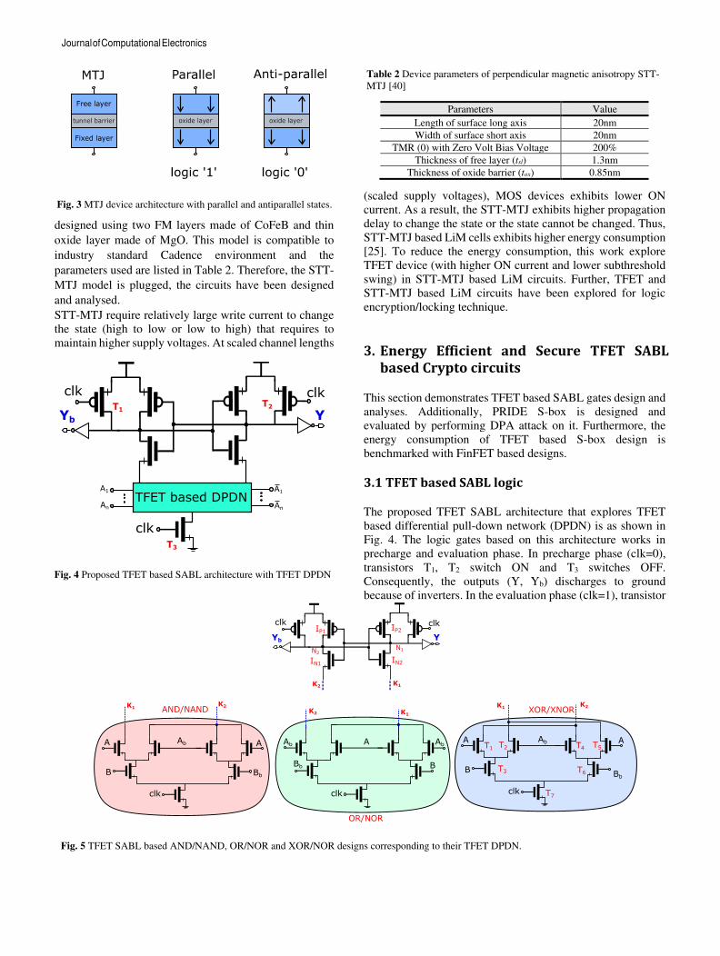
2.2 STT-MTJ Device Characteristics
Magnetic tunnel junction (MTJ) is a nano-stacked
structure that consists of two ferromagnetic (FM) layers,
separated by a thin oxide layer as shown in Fig. 3 [19].
Among two FM layers, the magnetic orientation of one
layer is fixed and it is named as reference layer.
Conversely, the magnetic orientation of other layer varies in
same or opposite direction to that of the reference layer, named
as free layer. Upon providing sufficient current through MTJ,
the magnetic orientation of free layer can be changed. When
the magnetic orientation of free layer and reference layer point
in the same direction, MTJ exhibits lower resistance (RP) and
it is called as parallel state. In contrast, if the magnetic
orientation of free layer and reference layer point in opposite
direction, MTJ exhibits higher resistance (RAP) and it is called
as anti-parallel state. Due to the non-magnetic layer, MTJ
exhibits variation in resistance, it is defined as tunnel magneto
resistance (TMR) (Equation 1). MTJ is supposed to exhibit
high TMR for faithful reproduction of stored value.
P
PAP
R
RRTMR
−= (1)
Among several switching mechanisms available, spin transfer
torque (STT) switching exhibits high TMR that is suitable to
commercialize MTJs [20]. The perpendicular STT-MTJ
devices eliminate the several challenges exhibited by in-plane
devices. As a result, perpendicular STT-MTJ devices have
attracted wide attention. This work explore a compact Verilog-
A model of CoFeB/MgO perpendicular magnetic anisotropy
STT-MTJ [21, 40]. The STT-MTJ described in this model is
Fig. 2 The N-TFET ID-VGS characteristics demonstrating (a) Higher ON current (b) Lower subthreshold swing (steep switching characteristics).
Table 1 Device parameters of InAs TFET and FinFET [30, 39]
TFET Parameters Value
Channel length 20nm
Effective oxide thickness (EoT) 0.7nm
Channel thickness (Tch) 5nm
Source Doping(InAs) 4×1019 cm-3
Drain Doping(InAs) 6×1017 cm-3
FinFET Parameters Value
Channel length 20nm
Effective oxide thickness (EoT) 0.7nm
Fin width (WFin) 8nm
Fin height(HFin) 25nm
Source/Drain Doping 1×1020 cm-3
Fig. 1 Device architectures of (a) N-TFET (b) N-FinFET
Journal of Computational Electronics
designed using two FM layers made of CoFeB and thin
oxide layer made of MgO. This model is compatible to
industry standard Cadence environment and the
parameters used are listed in Table 2. Therefore, the STT-
MTJ model is plugged, the circuits have been designed
and analysed.
STT-MTJ require relatively large write current to change
the state (high to low or low to high) that requires to
maintain higher supply voltages. At scaled channel lengths
(scaled supply voltages), MOS devices exhibits lower ON
current. As a result, the STT-MTJ exhibits higher propagation
delay to change the state or the state cannot be changed. Thus,
STT-MTJ based LiM cells exhibits higher energy consumption
[25]. To reduce the energy consumption, this work explore
TFET device (with higher ON current and lower subthreshold
swing) in STT-MTJ based LiM circuits. Further, TFET and
STT-MTJ based LiM circuits have been explored for logic
encryption/locking technique.
3. Energy Efficient and Secure TFET SABL
based Crypto circuits
This section demonstrates TFET based SABL gates design and
analyses. Additionally, PRIDE S-box is designed and
evaluated by performing DPA attack on it. Furthermore, the
energy consumption of TFET based S-box design is
benchmarked with FinFET based designs.
3.1 TFET based SABL logic
The proposed TFET SABL architecture that explores TFET
based differential pull-down network (DPDN) is as shown in
Fig. 4. The logic gates based on this architecture works in
precharge and evaluation phase. In precharge phase (clk=0),
transistors T1, T2 switch ON and T3 switches OFF.
Consequently, the outputs (Y, Yb) discharges to ground
because of inverters. In the evaluation phase (clk=1), transistor
Table 2 Device parameters of perpendicular magnetic anisotropy STT-
MTJ [40]
Parameters Value
Length of surface long axis 20nm
Width of surface short axis 20nm
TMR (0) with Zero Volt Bias Voltage 200%
Thickness of free layer (tsl) 1.3nm
Thickness of oxide barrier (tox) 0.85nm
Fig. 4 Proposed TFET based SABL architecture with TFET DPDN
Fig. 3 MTJ device architecture with parallel and antiparallel states.
Fig. 5 TFET SABL based AND/NAND, OR/NOR and XOR/NOR designs corresponding to their TFET DPDN.
Journal of Computational Electronics
T3 switches ON and connects the TFET DPDN to ground.
Depending upon the inputs applied to TFET based DPDN,
the outputs (Y, Yb) of SABL gates are evaluated.
Exploring the SABL architecture, TFET AND/NAND,
OR/NOR and XOR/NOR gates have been designed. The
logic gate designs corresponding to their TFET DPDN
circuits are shown in Fig. 5 where K1 and K2 are denoted
to indicate the connection between pull-up and pull-down
networks. For example, consider the TFET XOR gate
wherein input B is at logic ‘1’ and Bb is at logic ‘0’. As input A is at logic ‘0’ and Ab is at logic ‘1’, the node N1
discharges (through transistor T2 and T3) faster compared
to node N2. As a result, the transistor IP1 in the inverter
design (in pull-up network) switches ON and output Yb
discharges to ground. When Yb discharges to gnd, Y
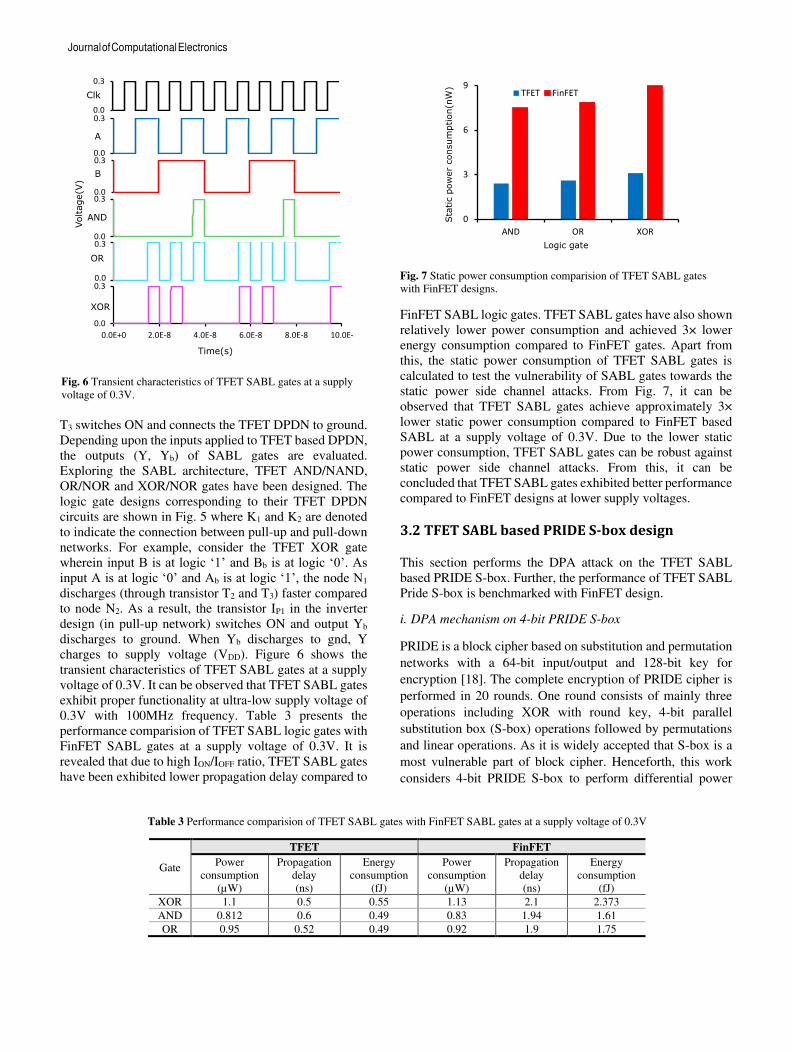
charges to supply voltage (VDD). Figure 6 shows the
transient characteristics of TFET SABL gates at a supply
voltage of 0.3V. It can be observed that TFET SABL gates
exhibit proper functionality at ultra-low supply voltage of
0.3V with 100MHz frequency. Table 3 presents the
performance comparision of TFET SABL logic gates with
FinFET SABL gates at a supply voltage of 0.3V. It is
revealed that due to high ION/IOFF ratio, TFET SABL gates
have been exhibited lower propagation delay compared to
FinFET SABL logic gates. TFET SABL gates have also shown
relatively lower power consumption and achieved 3× lower
energy consumption compared to FinFET gates. Apart from
this, the static power consumption of TFET SABL gates is
calculated to test the vulnerability of SABL gates towards the
static power side channel attacks. From Fig. 7, it can be
observed that TFET SABL gates achieve approximately 3×
lower static power consumption compared to FinFET based
SABL at a supply voltage of 0.3V. Due to the lower static
power consumption, TFET SABL gates can be robust against
static power side channel attacks. From this, it can be
concluded that TFET SABL gates exhibited better performance
compared to FinFET designs at lower supply voltages.
3.2 TFET SABL based PRIDE S-box design
This section performs the DPA attack on the TFET SABL
based PRIDE S-box. Further, the performance of TFET SABL
Pride S-box is benchmarked with FinFET design.
i. DPA mechanism on 4-bit PRIDE S-box
PRIDE is a block cipher based on substitution and permutation
networks with a 64-bit input/output and 128-bit key for
encryption [18]. The complete encryption of PRIDE cipher is
performed in 20 rounds. One round consists of mainly three
operations including XOR with round key, 4-bit parallel
substitution box (S-box) operations followed by permutations
and linear operations. As it is widely accepted that S-box is a
most vulnerable part of block cipher. Henceforth, this work
considers 4-bit PRIDE S-box to perform differential power
Table 3 Performance comparision of TFET SABL gates with FinFET SABL gates at a supply voltage of 0.3V
Gate
TFET FinFET
Power
consumption
(µW)
Propagation
delay
(ns)
Energy
consumption
(fJ)
Power
consumption
(µW)
Propagation
delay
(ns)
Energy
consumption
(fJ)
XOR 1.1 0.5 0.55 1.13 2.1 2.373
AND 0.812 0.6 0.49 0.83 1.94 1.61
OR 0.95 0.52 0.49 0.92 1.9 1.75
Fig. 6 Transient characteristics of TFET SABL gates at a supply
voltage of 0.3V.
Fig. 7 Static power consumption comparision of TFET SABL gates
with FinFET designs.
Journal of Computational Electronics
analysis attack [18]. The 4-input and 4-output PRIDE S-
box is a combinational block and the relation between
inputs and outputs is expressed as the boolean equations
(2-5).
2313 xxxy = (2)
1202 xxxy = (3)
2331 yyxy = (4)
2120 yyxy = (5)
The DPA attack is performed to retrieve the secret key
information of crypto engine. The adversary contains the
cryptographic algorithm with required input patterns to be
applied. The DPA attack is performed on PRIDE S-box
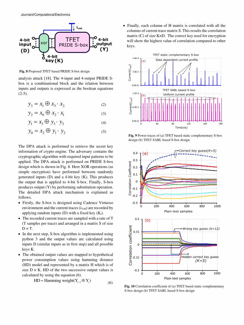
design which is shown in Fig. 8. Here XOR operations (as
simple encryption) have performed between randomly
generated inputs (D) and a 4-bit key (K). This produces
the output that is applied to 4-bit S-box. Finally, S-box
produces output (Y) by performing substitution operation.
The detailed DPA attack mechanism is explained as
follows.
• Firstly, the S-box is designed using Cadence Virtuoso
environment and the current traces (iVdd) are recorded by
applying random inputs (D) with a fixed key (Ki).
• The recorded current traces are sampled with a rate of T
(T samples per trace) and arranged in a matrix S of size
D × T.
• In the next step, S-box algorithm is implemented using
python 3 and the output values are calculated using
inputs D (similar inputs as in first step) and all possible
keys K.
• The obtained output values are mapped to hypothetical
power consumption values using hamming distance
(HD) model and represented by a matrix H which is of
size D × K. HD of the two successive output values is
calculated by using the equation (6).
1HD Hamming weight(Y Y )i i−= (6)
• Finally, each column of H matrix is correlated with all the
columns of current trace matrix S. This results the correlation
matrix (C) of size K×D. The correct key used for encryption
will show the highest value of correlation compared to other
keys.
Fig. 8 Proposed TFET based PRIDE S-box design
Fig. 9 Power traces of (a) TFET based static complementary S-box
design (b) TFET SABL based S-box design.
Fig. 10 Correlation coefficient of (a) TFET based static complementary
S-box design (b) TFET SABL based S-box design
Journal of Computational Electronics
ii. Security evaluation of TFET SABL based PRIDE S-box
The PRIDE S-box circuit is designed using proposed
TFET SABL gates. The proposed TFET SABL based
PRIDE S-box is compared with TFET based static
complementary PRIDE S-box to highlight the security
benefits. Both the designs have been implemented using
20nm InAs TFET technology. Each design individually
simulated using 100 random inputs with a fixed key
(K=5). The power traces which are obtained from the
TFET static and SABL based S-box circuits have been
depicted in Fig. 9. From this, it can be observed that the
power traces of TFET SABL based S-box circuit have
proved to be uniform compared to TFET based static
complementary design. The obtained power traces have
been sampled with a rate of 1000 and arranged as a matrix
S. The resulted power trace matrix S is correlated with the
hypothetical power values matrix (H) by following the
DPA mechanism. Figure 10(a) shows resultant correlation
coefficients of TFET based static complementary S-box
design with all possible keys. It can be seen that the DPA
attack performed on this design is successful and shows
highest correlation coefficient for the correct key (K=5).
Besides, the DPA attack performed on TFET SABL based
S-box design is observed to be unsuccessful as shown in
Fig. 10(b). The correlation coefficient of wrong key
(K=12) is observed to be high compared to the original key
(K=5). Moreover, the correlation coefficient of original
key is hidden in the analysis result and cannot be observed
by the adversary. This robustness is obtained from the
favourable SABL structure and the sharp switching
behaviour of TFET device.
iii. Performance benchmarking
The performance of TFET SABL based S-box design is
benchmarked with equivalent FinFET SABL based S-box
design as shown in Table 4. At a supply voltage of 0.3V,
TFET and FinFET based designs have shown an energy
consumption of 13.09fJ and 41.229fJ respectively. Thus,
TFET SABL based S-box design exhibited 3.15× lower
energy consumption compared to FinFET design at a
supply voltage of 0.3V. Moreover, static power
consumption of TFET SABL based S-box design is observed
to be 3.5× lower compared to FinFET design. Due to this,
TFET SABL based crypto circuits can exhibit lower
vulnerability to static power side channel attacks.
4. STT-MTJ and TFET Logic-in-Memory (LiM)
cells for Logic locking
This section presents the STT-MTJ and TFET based LiM gates
and benchmarked with the STT-MTJ and FinFET based
designs. Further, these gates are applied to logic
locking/encryption and energy consumption is calculated.
Moreover, the fabrication compatibility and challenges of
TFET and STT-MTJ have been discussed.
4.1 STT-MTJ and TFET LiM based logic gates
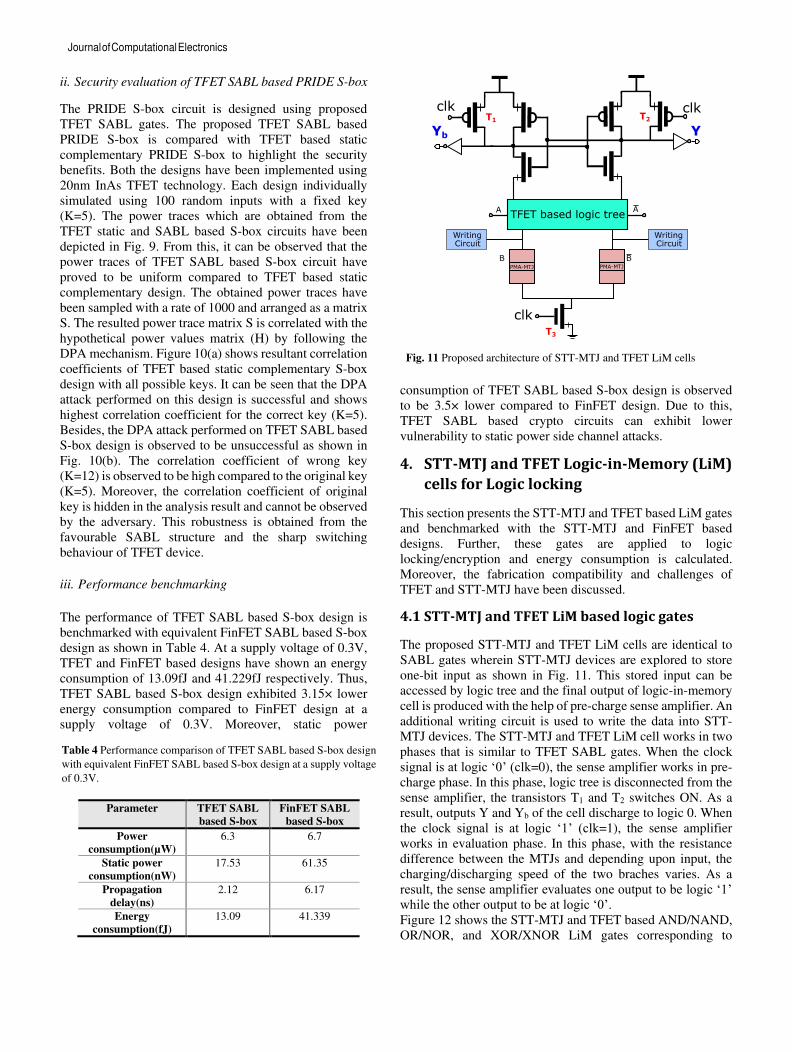
The proposed STT-MTJ and TFET LiM cells are identical to
SABL gates wherein STT-MTJ devices are explored to store
one-bit input as shown in Fig. 11. This stored input can be
accessed by logic tree and the final output of logic-in-memory
cell is produced with the help of pre-charge sense amplifier. An
additional writing circuit is used to write the data into STT-
MTJ devices. The STT-MTJ and TFET LiM cell works in two
phases that is similar to TFET SABL gates. When the clock
signal is at logic ‘0’ (clk=0), the sense amplifier works in pre-
charge phase. In this phase, logic tree is disconnected from the
sense amplifier, the transistors T1 and T2 switches ON. As a
result, outputs Y and Yb of the cell discharge to logic 0. When
the clock signal is at logic ‘1’ (clk=1), the sense amplifier
works in evaluation phase. In this phase, with the resistance
difference between the MTJs and depending upon input, the
charging/discharging speed of the two braches varies. As a
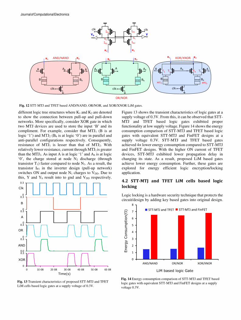
result, the sense amplifier evaluates one output to be logic ‘1’ while the other output to be at logic ‘0’. Figure 12 shows the STT-MTJ and TFET based AND/NAND,
OR/NOR, and XOR/XNOR LiM gates corresponding to
Table 4 Performance comparison of TFET SABL based S-box design
with equivalent FinFET SABL based S-box design at a supply voltage
of 0.3V.
Parameter TFET SABL
based S-box
FinFET SABL
based S-box
Power
consumption(µW)
6.3 6.7
Static power
consumption(nW)
17.53 61.35
Propagation
delay(ns)
2.12 6.17
Energy
consumption(fJ)
13.09 41.339
Fig. 11 Proposed architecture of STT-MTJ and TFET LiM cells
Journal of Computational Electronics
different logic tree structures where K1 and K2 are denoted
to show the connection between pull-up and pull-down
networks. More specifically, consider XOR gate in which
two MTJ devices are used to store the input ‘B’ and its compliment. For example, consider that MTJ1 (B is at
logic ‘1’) and MTJ2 (Bb is at logic ‘0’) are in parallel and anti-parallel configurations respectively. Consequently,
resistance of MTJ1 is lesser than that of MTJ2. With
relatively lower resistance, current through MTJ1 is greater
than the MTJ2. As input A is at logic ‘1’ and Ab is at logic
‘0’, the charge stored at node N2 discharge (through
transistor T1) faster compared to node N1. As a result, the
transistor IP2 in the inverter design (pull-up network)
switches ON and output node N1 charges to VDD. Due to
this, Y and Yb result into to gnd and VDD respectively.
Figure 13 shows the transient characteristics of logic gates at a
supply voltage of 0.3V. From this, it can be observed that STT-
MTJ and TFET based logic gates exhibited proper
functionality at low supply voltage. Figure 14 shows the energy
consumption comparison of STT-MTJ and TFET based logic
gates with equivalent STT-MTJ and FinFET designs at a
supply voltage 0.3V. STT-MTJ and TFET based gates
achieved 4× lower energy consumption compared to STT-MTJ
and FinFET designs. With the higher ON current of TFET
devices, STT-MTJ exhibited lower propagation delay in
changing its state. As a result, proposed LiM based gates
achieve lower energy consumption. Further, these gates are
explored for energy efficient logic encryption/locking
application.
4.2 STT-MTJ and TFET LiM cells based logic
locking
Logic locking is a hardware security technique that protects the
circuit/design by adding key based gates into original design.
Fig. 13 Transient characteristics of proposed STT-MTJ and TFET
LiM cells based logic gates at a supply voltage of 0.3V.
Fig. 12 STT-MTJ and TFET based AND/NAND, OR/NOR, and XOR/XNOR LiM gates.
Fig. 14 Energy consumption comparison of STT-MTJ and TFET based
logic gates with equivalent STT-MTJ and FinFET designs at a supply
voltage 0.3V.
Journal of Computational Electronics
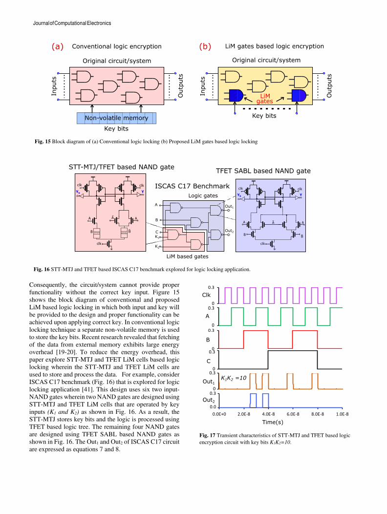
Consequently, the circuit/system cannot provide proper
functionality without the correct key input. Figure 15
shows the block diagram of conventional and proposed
LiM based logic locking in which both input and key will
be provided to the design and proper functionality can be
achieved upon applying correct key. In conventional logic
locking technique a separate non-volatile memory is used
to store the key bits. Recent research revealed that fetching
of the data from external memory exhibits large energy
overhead [19-20]. To reduce the energy overhead, this
paper explore STT-MTJ and TFET LiM cells based logic
locking wherein the STT-MTJ and TFET LiM cells are
used to store and process the data. For example, consider
ISCAS C17 benchmark (Fig. 16) that is explored for logic
locking application [41]. This design uses six two input-
NAND gates wherein two NAND gates are designed using
STT-MTJ and TFET LiM cells that are operated by key
inputs (K1 and K2) as shown in Fig. 16. As a result, the
STT-MTJ stores key bits and the logic is processed using
TFET based logic tree. The remaining four NAND gates
are designed using TFET SABL based NAND gates as
shown in Fig. 16. The Out1 and Out2 of ISCAS C17 circuit
are expressed as equations 7 and 8.
Fig. 15 Block diagram of (a) Conventional logic locking (b) Proposed LiM gates based logic locking
Fig. 16 STT-MTJ and TFET based ISCAS C17 benchmark explored for logic locking application.
Fig. 17 Transient characteristics of STT-MTJ and TFET based logic
encryption circuit with key bits K1K2=10.
Journal of Computational Electronics
( )11 .KCBCAOut += (7)
( ) ( )212 . KBKCOut += (8)
For example, the key bits K1K2 are fixed as “10”, the
equations 7 and 8 are simplified as equations 9 and 10
CBCAOut +=1 (9)
CBOut =2 (10)
Figure 17 shows the transient characteristics of proposed
ISCAS C17 based circuit at a supply voltage of 0.3V.
With key bits of K1K2 = “10”, the circuit shows correct functionality as mentioned in equation 9 and 10. The
energy consumption of STT-MTJ and TFET LiM cells
based C17 circuit is calculated at a supply voltage of 0.3V.
It can be observed that STT-MTJ and TFET based logic
encryption circuit achieves a lower energy consumption of
6.96fJ. On the other hand, STT-MTJ and FinFET based
logic encryption circuit shows energy consumption of
21.64fJ. From this, it can be seen that proposed design
shows 3.11× lower energy consumption compared to
FinFET designs. STT-MTJ and TFET LiM based logic
encryption achieves lower energy consumption due to the
higher ON current and low leakage characteristics of
TFET at lower supply voltages.
4.3 Fabrication Compatibility of STT-MTJ with
TFET
The homo-junction TFET and CMOS FinFET devices
have been fabricated using identical manufacturing
process since architecture of both devices is observed to
be similar [28]. It is experimentally proved that
complementary TFET devices fabricated in standard
CMOS foundry exhibited higher compatibility for
commercial production and enhanced flexibility for
heterogeneous TFET-CMOS systems [28]. Several
research groups have demonstrated the benefits of mixed
MOSFET-TFET circuits/systems and corresponding
layout rules with both simulations and experimental
fabrication [31]. Besides, STT-MTJ exhibits higher
compatibility with CMOS process by fabricating them in
back-end-of-the-line. This encouraged the researches to
explore logic-in-memory architectures that achieve low
area and energy overheads. Recent research demonstrated
the heterogeneous 3D integration for STT-MTJ based
memory-on-logic applications that separates memory,
logic blocks and stacks memory tire on top of logic block
[20]. This STT-MTJ based 3D integration achieved silicon
area saving with performance gain.
CMOS exhibited higher compatibility with STT-MTJ and
TFET is fabricated using identical manufacturing like
CMOS. Therefore, the TFET technology can show ease of
integration and flexibility in manufacturing with STT-
MTJ. However, secondary effects including ambipolarity, p-i-
n forward current and enhanced miller effect still exist in TFET
which make it unpopular and less suitable for
commercialization now [31]. More research efforts are require
to make these emerging technology integration a reality.
5. Conclusion
Existing CMOS SABL based circuits and CMOS based STT-
MTJ LiM circuits exhibited large energy consumption with
increased vulnerability towards hardware security attacks. To
reduce the energy consumption, emerging TFET is introduced
into these circuits that achieved ultra-low energy consumption
with enhanced security. TFET SABL based gates and PRIDE
S-box design achieve approximately 3× lower energy
consumption compared to FinFET designs while maintaining
higher DPA resilience. Moreover, TFET SABL based crypto
systems with lower static power consumption can show
vulnerability to static power side-channel attacks.
Additionally, proposed STT-MTJ and TFET LiM gates
achieves 4× lower energy consumption compared to STT-MTJ
and FinFET designs. The proposed STT-MTJ and TFET LiM
gates have been explored in logic encryption/locking technique
that shows 3× lower energy consumption compared to STT-
MTJ and FinFET designs. STT-MTJ and TFET based circuits
have exhibited higher compatibility in fabrication. However,
STT-MTJ and TFET devices exhibited several second order
effects including low reliability, process variations and other
leakages (ambipolarity and p-i-n forward current) that make
commercialization of these devices difficult. More research
efforts are required in future from the device-circuit
community to resolve the existing challenges.
References
1. Li, A., Shinde, Y., Shi, J., Ye, X., Y. Li., and W. Z. Song.: System
Statistics Learning-Based IoT Security: Feasibility and Suitability.
IEEE J. Internet of Things. 6(4), 6396-6403 (2019).
2. The Cost of Malicious Cyber Activity to the US Economy, W. House,
2018. [Online].
Available:https://www.whitehouse.gov/wpcontent/uploads/2018/03/T
he-Cost-of-Malicious-Cyber-Activity-to-the-U.S.-Economy.pdf
3. Bartock, M., Souppaya, M., Savino, R., Knoll, T., Shetty, U.,
Cherfaoui, M., Yeluri, R. and Scarfone, K.: Hardware-Enabled
Security for Server Platforms: Enabling a Layered Approach to
Platform Security for Cloud and Edge Computing Use Cases. National
Institute of Standards and Technology. (pp. 39-39).
4. Roshanisefat, S., Kamali, H. M., Homayoun, H., and Sasan, A.: SAT-
hard Cyclic Logic Obfuscation for Protecting the IP in the
Manufacturing Supply Chain. IEEE Trans. VLSI Syst. 28(4), 954-967
(2020).
5. Prinetto, P., and Roascio, G.: Hardware Security, Vulnerabilities, and
Attacks: A Comprehensive Taxonomy. In ITASEC.177-189 (2020).
6. De, P., Mandal, C., and Prampalli, U.: Path-Balanced Logic Design to
Realize Block Ciphers Resistant to Power and Timing Attacks. IEEE
Trans. VLSI Syst. 27(5), 1080-1092 (2019).
7. Wang, W., Standaert, Y. F. X., Liu, J., Guo, Z., and Gu, D.: Ridge-
Based DPA: Improvement of Differential Power Analysis For
Nanoscale Chips. IEEE Trans. Inform. Forensics and Security. 13(5),
1301-1316 (2018).
8. Rossi, D., Tenentes,V., Yang, S., Khursheed S., and Al-Hashimi, B.
Journal of Computational Electronics
M.: Aging Benefits in Nanometer CMOS Designs. In IEEE
Trans. on Circuits and Systems II: Express Briefs. 64(3), 324-
328(2017).
9. De Cnudde, T., Nikova, S.: Securing the present block cipher
against combined side-channel analysis and fault attacks. IEEE
Trans. Very Large Scale Integ. Syst., 25(12), 3291–3301(2017).
10. Shanmugham, S. R., and Paramasivam, S.: Survey on power
analysis attacks and its impact on intelligent sensor
networks. IET Wireless Sensor Systems, 8(6), 295-304 (2018).
11. Tena-Sanchez, E., Castro, J., and Acosta, A. J.: A Methodology
for Optimized Design of Secure Differential Logic Gates for
DPA Resistant Circuits. IEEE J. Emerg. Select. Topics Circuits
Syst. 4(2), pp. 203–215 (2014).
12. Kumar, S. D., Thapliyal, H., and Mohammad, A.: FinSAL: A
novel FinFET based Secure Adiabatic Logic for energy-efficient
and DPA resistant IoT devices. IEEE Trans. Comput.-Aided
Design Integr. Circuits and Syst. 37(1), 2017.
13. Avital, M., Dagan, H., Keren, O., and Fish, A.: Randomized
Multitopology Logic Against Differential Power Analysis. In
IEEE Trans. on VLSI Syst., 23(4), 702-711(2015).
14. Tanimura, K., and Dutt, N. D.: HDRL: Homogeneous Dual-Rail
Logic for DPA Attack Resistive Secure Circuit Design. In IEEE
Embedded Systems Letters, 4(3), 57-60 (2012).
15. Kumar, S. D., Thapliyal, H., and Mohammad, A.: EE-SPFAL: A
Novel Energy-Efficient Secure Positive Feedback Adiabatic
Logic for DPA Resistant RFID and Smart Card. IEEE Trans.
Emerging Topics in Comput. 7(2), 281–293(2019).
16. Saini, H., and Gupta, A.: Constant Power Consumption Design
of Novel Differential Logic Gate for Immunity against
Differential Power Analysis. IET Circuits, Devices & Syst. 13(1),
103–109(2018).
17. Bellizia, D., Bongiovanni, S., Monsurro, P., Scotti, G., and
Trifiletti, A.: Univariate Power Analysis Attacks Exploiting
Static Dissipation of Nanometer CMOS VLSI Circuits for
Cryptographic Applications. IEEE Trans. Emerging Topics in
Comput. 5(3), 329-339(2017).
18. Delgado-Lozano, I. M., Tena-Sanchez, E., Nunez J., and Acosta,
A. J.: Design and Analysis of Secure Emerging Crypto-Hardware
using HyperFET Devices. IEEE Trans. Emerg. Topics in
Comput. (2020).
19. Hanyu, T., Endoh, T., Suzuki, D., Koike, H., Ma, Y., Onizawa,
N., Natsui, M., Ikeda, S. and Ohno, H.: Standby-power-free
integrated circuits using MTJ-based VLSI computing. Proc. of
the IEEE. 104(10), 1844-1863(2016).
20. Zhu, L., Bamberg, L., Agnesina, A., Catthoor, F., Milojevic, D.,
Komalan, M., Ryckaert, J., Garcia-Ortiz, A. and Lim, S.K.:
Heterogeneous 3D Integration for a RISC-V System With STT-
MRAM. IEEE Computer Architecture Lett. 19(1), 51-54(2020).
21. Shi, Y., Oh, S., Huang, Z., Lu, X., Kang, S.H. and Kuzum, D.:
Performance Prospects of Deeply Scaled Spin-transfer Torque
Magnetic Random-access Memory for In-memory
Computing. IEEE Electron Device Lett. (2020).
22. Deng, E., Zhang Y., Klein, J. O., Ravelsona, D., Chappert, C.,
Zhao, W.: Low power magnetic full-adder based on spin transfer
torque MRAM. IEEE Trans. on Magnet. 49(9), 4982-7(2013).
23. Deng, E., Zhang, Y., Kang, W., Dieny, B., Klein, J. O., Prenat,
G., Zhao, W.: Synchronous 8-bit non-volatile full-adder based on
spin transfer torque magnetic tunnel junction. IEEE Transactions
on Circuits and Systems I: Regular Papers. 62(7), 1757-65(2015).
24. Cai, H., Wang, Y., Naviner, L. A., Zhao, W.: Robust ultra-
low power non-volatile logic-in-memory circuits in FD-SOI
technology. IEEE Trans. on Circuits and Systems I: Regular
Papers. 64(4), 847-57(2016).
25. Natsui, M., Suzuki, D., Sakimura, N., Nebashi, R., Tsuji, Y.,
Morioka, A., Sugibayashi, T., Miura, S., Honjo, H.,
Kinoshita, K., Ikeda, S.: Nonvolatile logic-in-memory LSI
using cycle-based power gating and its application to motion-
vector prediction. IEEE Journal of Solid-State Circuits. 50(2), 476-
89(2014). 26. Kumar, S. D., and Thapliyal, H.: Exploration of Non-Volatile
MTJ/CMOS Circuits for DPA-Resistant Embedded Hardware. IEEE
Trans. Magnet., 55(12), 1-8(2019).
27. Resta, G.V., Leonhardt, A., Balaji, Y.: Devices and circuits using novel
2-D materials: a perspective for future VLSI systems. IEEE Trans.
VLSI Syst. 27(7), 1486–1503(2019).
28. Gopireddy, B., Skarlatos, D., Zhu, W., and Torrellas, J.: HetCore:
TFET-CMOS hetero-device architecture for CPUs and GPUs.
ACM/IEEE 45th Annual International Symposium on Computer
Architecture. 802-815(2018).
29. Kino, H., Fukushima, T., and Tanaka, T.: Generation of STDP With
Non-Volatile Tunnel-FET Memory for Large-Scale and Low-Power
Spiking Neural Networks. In IEEE Journal of the Electron Devices
Society. 8, 1266-1271 (2020).
30. Aditya, J., Vallabhaneni, H., and Vaddi, R.: Reliability enhancement
of a steep slope tunnel transistor based ring oscillator designs with
circuit interaction. IET Circuits, Devices & Syst. 10(6), 522-
527(2016).
31. Lin Z., et al.: Challenges and Solutions of the TFET Circuit Design,
IEEE Trans. on Circuits and Systems I: Regular Papers. 67(12), 4918-
4931(2020).
32. Aditya, J., et al.: Tunneling Field Effect Transistors for Enhancing
Energy Efficiency and Hardware Security of IoT Platforms:
Challenges and Opportunities. In Proc. IEEE Int. Symp. Circuits and
Systems (ISCAS). 1-5(2018).
33. Bi, Y., et al.: Tunnel FET current mode logic for DPA-resilient circuit
designs. IEEE Trans. Emerg. Top. Comput. 5(3), 340–352(2017).
34. Thapliyal, H., Varun, T. S. S., and Dinesh Kumar, S.: Low-Power and
Secure Lightweight Cryptography Via TFET-Based Energy Recovery
Circuits. In Proc. IEEE Int. Conf. Rebooting Comput., Washington. 1-
4(2017).
35. Chen, A., et al.: Using emerging technologies for hardware security
beyond PUFs. In IEEE Design, Automation & Test Conf. &
Exhibition, Dresden. 1544–1549(2016).
36. Aditya, J., Majumder, M. K., Sahoo, S. K., and Vaddi, R. Tunnel FET
Ambipolarity-Based Energy Efficient and Robust True Random
Number Generator Against Reverse Engineering Attacks. IET
Circuits, Devices & Syst., 13(5), 689-695(2019).
37. Aditya, J., Majumder, M. K., Sahoo, S. K., and Vaddi, R. Low area
overhead DPA countermeasure exploiting tunnel transistor-based
random number generator. IET Circuits, Devices & Syst., 14(5), 640-
647(2020).
38. Aditya, J., Majumder, M. K., Sahoo, S. K., and Vaddi, R.: Tunnel
FET‐based ultralow‐power and hardware‐secure circuit design
considering p‐i‐n forward leakage. International Journal of Circuit
Theory and Applications, 48(4), 524-538(2020).
39. Liu, H., Narayanan, V., Datta, S, et al.: III-V Tunnel FET model.
version 1.0.1. 2015.
https://nanohub.org/publications/12/2
40. Zhang, Y., et al., “Compact Modeling of Perpendicular-Anisotropy
CoFeB/MgO Magnetic Tunnel Junctions,” in IEEE Trans. on Electron Devices. 59(3), 819-826 (2012).
41. Hansen, M. C., Yalcin, H., and Hayes, J. P.: Unveiling the ISCAS-85
benchmarks: A case study in reverse engineering. IEEE Design & Test
of Comput., 16(3), 72-80, (1999).

Journal of Computational Electronics