energy frontier research center for solid-state lighting...
TRANSCRIPT

Energy Frontier Research Center for Solid-State Lighting Science:Exploring New Materials Architectures and Light EmissionPhenomenaMichael E. Coltrin,*,† Andrew M. Armstrong,† Igal Brener,† Weng W. Chow,† Mary H. Crawford,†
Arthur J. Fischer,† David F. Kelley,‡ Daniel D. Koleske,† Lincoln J. Lauhon,§ James E. Martin,†
May Nyman,∥ E. Fred Schubert,⊥ Lauren E. Shea-Rohwer,† Ganapathi Subramania,† Jeffrey Y. Tsao,†
George T. Wang,† Jonathan J. Wierer, Jr.,† and Jeremy B. Wright†
†Sandia National Laboratories, P.O. Box 5800, MS-1086, Albuquerque, New Mexico 87185-1086, United States‡Chemistry and Chemical Biology, University of California Merced, Merced, California 95343, United States§Department of Materials Science and Engineering, Northwestern University, Evanston, Illinois 60208, United States∥Department of Chemistry, Oregon State University, Corvallis, Oregon 87331, United States⊥Department of Electrical, Computer and Systems Engineering, Rensselaer Polytechnic Institute, Troy, New York 12180, UnitedStates
ABSTRACT: The Energy Frontier Research Center (EFRC) forSolid-State Lighting Science (SSLS) is one of 46 EFRCs initiated in2009 to conduct basic and use-inspired research relevant to energytechnologies. The overarching theme of the SSLS EFRC is theexploration of energy conversion in tailored photonic structures. Inthis article we review highlights from the research of the SSLS EFRC.Major research themes include: studies of the materials properties andemission characteristics of III-nitride semiconductor nanowires;development of new phosphors and II−VI quantum dots for use aswavelength downconverters; fundamental understanding of compet-ing radiative and nonradiative processes in current-generation, planarlight-emitting diode architectures; understanding of the electrical,optical, and structural properties of defects in InGaN materials andheterostructures; exploring ways to enhance spontaneous emission through modification of the environment in which theemission takes place; and investigating routes such as stimulated emission that might outcompete nonradiative processes.
■ INTRODUCTION
Artificial light has long been a significant factor contributing tothe quality and productivity of human life.1 As a consequence,human civilization uses huge amounts of energy to produce it.Today, artificial light consumes an estimated 0.72% of worldGDP and, due to its high energy intensity, an estimated 6.5% ofworld primary energy and 16% of world electrical energy.1
Solid-state lighting is an emerging technology in which solid-state devices, like light-emitting diodes (LEDs) or laser diodes(LDs), are used to produce artificial light for generalillumination. Solid-state lighting (SSL) efficiencies haveincreased steadily over the past decade and are now greaterthan those of incandescent and fluorescent lamps.2 However,commercial SSL is still only ∼25% efficient, and there is thusmuch room for further improvement.To help lay the scientific foundations for that improvement,
the Energy Frontier Research Center (EFRC) for Solid-StateLighting Science (SSLS) was one of 46 EFRCs initiated in 2009to conduct basic and use-inspired research relevant to energytechnologies. The overarching theme of this center is
“exploring energy conversion in tailored photonic structures”,and in this article we review highlights from the research of theSSLS EFRC.Figure 1 presents a sketch of a common state-of-the-art
commercial white solid-state lamp, along with the spectralpower density of its emission. The lamp consists of a blue LED,1-square-mm in size, driven with 0.7 A of current, and coatedwith green and red phosphors.3 Some of the blue light from theLED leaks through the phosphors, giving the relatively narrowblue peak in the spectral power density. However, some bluelight is absorbed by the phosphors and is re-emitted as greenand red light, giving the two relatively wide green and red peaksin the spectral power density. The combination of blue, green,and red light is both pleasing to the human eye and faithfullyrenders colors of viewed objects. The lamp’s ∼25% efficiency isdue to the cumulative effect of three subefficiencies,4 with the
Received: January 31, 2014Revised: April 8, 2014Published: April 22, 2014
Feature Article
pubs.acs.org/JPCC
© 2014 American Chemical Society 13330 dx.doi.org/10.1021/jp501136j | J. Phys. Chem. C 2014, 118, 13330−13345

contribution of each subefficiency identifiable with a particularSSL technology challenge (A−C in Figure 1).The first subefficiency is that of the blue LED, which is
currently ∼43% at a current density of ∼700 mA into a mm2
chip for the illustrated device. This is much lower than the bestthus-far-reported lab result, 81%, for a much lower currentdensity5 (25 mA/mm2), due to an “efficiency droop”adecrease in efficiency with increased injected-current density,which is the subject of intense research interest.6 We use herethe subefficiency at the higher current density because highercurrent densities (at least 700 mA and ideally 2 A into a mm2
chip) are desirable to defray the manufacturing cost of the SSLchip. So a first SSL technology challenge (A in Figure 1) is toincrease blue LED efficiency, particularly at high currentdensities.The second subefficiency, that of the phosphors and package,
is about 70%. Some of this is because the phosphors do nothave perfect quantum yield; that is, one blue photon in doesnot result in one red or green photon out. However, quantumyields are improving, leaving a more fundamental efficiencyloss, the so-called Stokes deficit, which is the quantum energydeficit associated with converting a blue into a red or greenphoton. One way of eliminating this loss would be to eliminatephosphors altogether through use of direct electroluminescent(EL) emitters. However, the current state-of-the-art visibleelectroluminescent semiconductors, InGaN and InGaAlP, havelow efficiencies in the red−yellow−green spectral rangenecessary for high-color-quality white light. Thus, a secondSSL technology challenge (B in Figure 1) is to fill the red−yellow−green (RYG) gap in semiconductor electrolumines-cence.The third subefficiency is associated with the match between
the spectrum of emitted white light and the human eyesensitivity and is of the order ∼85%. The red phosphor (dashedred curve in Figure 1) used in the white lamp is centered at awavelength of 615 nm, which is the ideal peak emissionwavelength at the red end of the spectrum to provide goodcolor rendering. However, current phosphors also emit quite farinto the deep redso deep that the human eye is not verysensitive to it, as can be seen from the human eye response(dashed pink curve in Figure 1). This spillover into the deepred due to the broad phosphor emission accounts for the loss in“efficiency” due to the LED emission spectrum.7,8 So, a thirdSSL technology challenge (C in Figure 1) is to find an efficientnarrow-line-width red wavelength downconverter.
Note that there is one subefficiency that does not enter intothe overall ∼25% lamp efficiency but that we mention here forcompleteness: the subefficiency associated with the intelligentmatching of light to its use. By intelligence we mean control ofthe artificial light so that it is on only when it is being used andis directed only where it is needed.9 And, when and where it isbeing used, the intensity, chromaticity, and perhaps even thecolor rendering quality and luminous efficacy of the artificiallight could all potentially be optimized to how it is being used.So a fourth SSL technology challenge (D in Figure 1) iscreating light with this kind of intelligence.
■ OVERVIEW OF RESEARCH CHALLENGES:MATERIALS ARCHITECTURES ANDLIGHT-EMISSION PHENOMENA
Although the three subefficiencies may not seem unacceptablylow (43%, 70%, and 85%), due to their serial nature, theirmultiplicative effect is a net overall efficiency around 25%.Overcoming the three SSL technology challenges is thusextremely important. The goal of the SSLS EFRC is 2-fold: (a)to gain a deeper understanding of the materials architecturesand light-emission phenomena used in current-day SSLapproaches and (b) to explore new materials architecturesand light-emission phenomena that have the potential forbreakthroughs in energy efficiency. To do this, the SSLS EFRCis organized around six Research Challenges. As illustrated inFigure 2, two of the Research Challenges are focused onmaterials architectures, and four of the Research Challenges arefocused on light-emission phenomena.
The two materials architecture Research Challenges areillustrated at the top of Figure 2, the first of which is the“Nanowires” Research Challenge. Because of their narrowdiameters, nanowires have the potential to be fabricatedwithout line defects and can accommodate more strain andtherefore a wider range of compositions, including those thatmight enable high-efficiency green, yellow, and red lightemission. The second materials architecture Research Chal-lenge is “Quantum Dots and Phosphors,” with applications towavelength downconversion, particularly for narrow-line-widthred emission.The four light-emission phenomena Research Challenges are
illustrated at the bottom of Figure 2. To put these four incontext, Figure 2 shows the equation that parses out the variouscontributions to power-conversion efficiency of a light-emittingdevice. There is a Joule efficiency associated with resistive lossesas carriers are transported from electrical contacts to the active
Figure 1. Sketch of a common state-of-the-art commercial white solid-state lamp, along with its emission spectral power density. (Withpermission of John Wiley & Sons, Inc.; photo credit http://bobbymercerbooks.com/).
Figure 2. Schematic of the SSLS EFRC’s six Research Challenges. Thetwo at the top are focused on materials architectures, and the four atthe bottom are focused on light-emission phenomena.
The Journal of Physical Chemistry C Feature Article
dx.doi.org/10.1021/jp501136j | J. Phys. Chem. C 2014, 118, 13330−1334513331

region of the device. Then there is an injection efficiencyassociated with whether, once the carriers get to the activeregion, they overshoot it or thermalize in it or if they dothermalize in it they then for whatever reason escape. Thenthere is an internal quantum efficiency associated with thefraction carriers that recombine radiatively (the spontaneousemission Bn2 term, where n is carrier density) rather thannonradiatively (the defect-mediated An and Auger recombina-tion Cn3 terms). Finally, there is the extraction efficiencythefraction of photons that are created in the device that escape.The first two light-emission phenomena Research Challenges
(in blue) focus on these various competing processes:“Competing Radiative and Nonradiative Processes” , examinesthe overall competition between the processes; “Defect−Carrier Interactions” examines one of the most importantand fundamental of the processes, defect-mediated carrierrecombination.The second two light-emission phenomena Research
Challenges (in green) focus on ways to alter internal quantumefficiency to better compete with parasitic nonradiative carrierrecombination: “Enhanced Spontaneous Emission” exploresways of enhancing spontaneous emission through modificationof the environment within which the emission takes place;“Beyond Spontaneous Emission” explores the possibility ofgoing beyond spontaneous emission, through the addition ofcavities and coherent processes, such as lasing.
■ MATERIALS ARCHITECTURES: NANOWIRES
Our “Nanowires” Research Challenge explores the synthesisand properties of GaN/InGaN nanowires (NWs) as a newmaterials architecture for visible-light emission. Among themany advantages of GaN/InGaN nanowires over presentlyemployed planar GaN/InGaN films are the potential for high-quality material, without detrimental line defects; the ability toaccommodate lattice strain and therefore a wider range of alloycompositions and bandgaps; manipulability of growth geo-metries to expose surface orientations with tailored light-emission properties and reduced piezoelectric fields; the largesidewall surface area available for active light emission; and theability to create novel mesoscale structures such as photoniccrystals. If nanowire light emitters could span the entire visiblespectrum, the RYG-gap technology challenge would beovercome. In addition, full-spectrum emission would enablechromaticity tunability for intelligent lighting.9 Table 1summarizes the unique properties of nanowires and theirpotential benefit for lighting. The advantages of semiconductornanowires for photonics10 and GaN-based nanowires forlighting have been previously reviewed in detail.11
That said, application of GaN/InGaN nanowires for SSL is arelatively immature area of research. Thus, this Research
Challenge is broad in scope, encompassing materials synthesisand processing of photo- and electroluminescent nanowires,including both axial and radial types, along with optical,electrical, mechanical, and structural characterization andmodeling.
Bottom-Up and Top-Down Synthesis Methods. GaN-based nanowires are typically synthesized through bottom-upmethods, including vapor−liquid−solid (VLS)12,13 and catalyst-free selective-area growth (SAG).14 Our early work was alongthese lines: Ni-catalyzed metalorganic chemical vapor deposi-tion (MOCVD)15,16 was used to synthesize vertically alignedGaN nanowires on (11 ̅12) r-plane sapphire wafers.17 Trans-mission electron microscopy (TEM) studies showed that thesenanowires were single crystalline and oriented along the [112 ̅0]direction, with isosceles triangular cross sections having twoequivalent {1 ̅101} facets and one N-polar (0001 ̅) c-plane facet.Promisingly, the nanowires were observed to be free ofthreading dislocations, though c-plane stacking faults were seen.Bottom-up methods, however, particularly for GaN-based
nanowires, require highly specific conditions, such as low V-to-III ratio, to promote anisotropic one-dimensional crystalgrowth. These growth conditions can potentially lead tolower overall crystal quality, the introduction of higher impurityand point defect densities, and less flexibility for adjustinggrowth conditions to control doping and composition.Thus, our more recent work has explored complementary
top-down methods. In particular, a new two-step top-downnanowire fabrication approach was developed that enables theformation of high-quality nanowire arrays with independentlycontrolled pitch, height, and diameter,18,19 as shown in Figure3. The first step of the process is an anisotropic plasma etch of a
c-plane GaN-based film through a self-assembled mask ofmonodisperse silica spheres (lithographically defined etchmasks can also be used) to define tapered c-axis-orientedGaN pillars. The second step of the process is a facet-selectivewet etch (using AZ400K photoresist developer) that removesthe plasma-etch damage and results in nanowires with straightand smooth sidewalls and with diameters controlled by the wetetch time. A general comparison of GaN-based bottom-up andtop-down fabricated nanowires, highlighting relative advantagesand disadvantages of each method, is provided in Table 2.In the remainder of this section we discuss some of the
highlights of our work on GaN and InGaN nanowire structures
Table 1. Summary of Nanowire Properties and PotentialBenefits for Lighting
nanowire property benefit for SSL
strain accommodation high In-content structuresreduced dislocation densitiesgrowth on lattice mismatched substrates
high surface/device area greatly increased areal device densitynonpolar sidewall facets eliminate quantum confined Stark effect2D arrangements possible photonic crystals for light extractionfreestanding optical cavity compact, low-power nanolasers possible
Figure 3. Array of GaN nanowires fabricated by a two-step dry pluswet top-down etching process.
The Journal of Physical Chemistry C Feature Article
dx.doi.org/10.1021/jp501136j | J. Phys. Chem. C 2014, 118, 13330−1334513332

synthesized through various combinations of bottom-up andtop-down methods.Minority (Hole) Carrier Diffusion Length. Light-emitting
devices often rely on transport of minority carriers in abackground of majority carriers. In the ideal case, the minoritycarrier diffusion length is determined by a competition betweenthe rate at which the minority carriers diffuse and the rate atwhich they recombine radiatively. In less ideal cases minoritycarriers can recombine nonradiatively at defects or surfaces,thus shortening the diffusion length. In nanowires, for whichsurfaces are nearby, this could be a major issue.To understand this basic issue, we studied hole minority
carrier diffusion lengths in GaN, GaN/AlGaN, and GaN/InGaN core−shell NWs grown by a two-step process: Ni-catalyzed axial MOCVD of a GaN core followed by radialMOCVD of an AlGaN or InGaN shell. The experiment madeuse of scanning electron microscopy to generate charge at aparticular position on the nanowire, combined with near-fieldscanning optical microscopy to observe the spatial profile of theluminescence away from the charge-generation position.The results were that, for GaN or GaN/InGaN nanowires,
minority carrier diffusion lengths were indeed shorter than whatwould be expected for bulk GaN, likely due to surfacerecombination. For GaN/AlGaN nanowires, however, minoritycarrier diffusion lengths were in the 1 μm range, on the order ofthat expected for bulk GaN, consistent with the AlGaN shellacting as a higher-bandgap carrier confinement layer for holesin the GaN core.20
Mechanical Resilience. Ideally, solid-state light emittersare driven “hard” to maximize lumen output per chip and tominimize chip cost per lumen. Nanowire emitters for solid-statelighting might also be driven hard and hence be subject tomechanical stresses due to thermal gradients or thermalexpansion mismatches in complex compositionally tailoredstructures. Moreover, new micro-opto-electromechanical(MOEM) functionalities that make use of strong piezoelectriceffects in GaN-based materials might also lead to significantmechanical stresses.To understand the response of nanowires to mechanical
stress, we studied the deformation, fracture mechanisms, andfracture strength of individual GaN NWs grown by Ni-catalyzed MOCVD. The measurements were made in a uniquetransmission electron microscope−scanning probe microscope(TEM−SPM) platform that enabled high-resolution real-timeimaging during deformation by a nanoscale “punch”.21
One important result was that GaN NWs were resistant toplastic deformation by dislocation nucleation and propagationnearly up to the point of fracture, and even near the point of
fracture, the lack of dislocation mobility in GaN causeddislocations to pile-up in, and plastic deformation to belocalized to, the material just underneath the punch. Thisbehavior is in strong contrast to that of metal NWs, in whichdislocations propagate easily and enable global, not just local,plastic deformation.22−27
A second important result was that the fracture strength ofthe NWs increased sharply with decreasing NW diameter: inthe 0.2 GPa range for 700 nm diameters to the 1.7 GPa rangefor 200 nm diameters. This result is curious and would beinteresting to study further but suggests that GaN NWs will bemechanically resilient in many applications, and the more sothe smaller their diameter.
Nanoscopically Nonuniform InGaN Shell Composi-tions. In many interesting nanowire configurations InGaNepitaxy on a nanostructure with anisotropic, faceted featuresmight be required. The different facets and their intersectionsmight have differing chemistries and nanoscopic local strains,differing In-to-Ga incorporation rates, and thus differingnanoscopic local InGaN alloy compositions.To explore this possible phenomenon, InGaN coaxial shells
were epitaxially grown on dislocation-free a-axis oriented GaNNWs, these NWs themselves grown via Ni-catalyzed MOCVD.The resulting nanoscopic local optical properties, indiumconcentrations, defect microstructures, and strain distributionsof the InGaN shells were investigated using a combination ofspatially resolved cathodoluminescence (CL), scanning trans-mission electron microscopy (STEM), and finite elementcomputational analysis.28
The results were that for InGaN epitaxy on the semipolar{1 ̅101} facets 40% or greater indium compositions could beobtained, with luminescence observed into the near-infraredwavelengths. Dislocations were observed, in the 108 cm−2 rangebut at a much lower density than usually associated with thehighly lattice-mismatched epitaxy of similar indium composi-tions on planar GaN surfaces.29
Indium was found to preferentially incorporate at the edgeintersections (corners) between nanowire facets, where finiteelement analysis indicates strain was favorably tensile, ratherthan on the nanowire facets themselves, where finite elementanalysis indicates strain was unfavorably compressive. This isconsistent with microscopic “lattice latching” or “compositionalpulling”, in which epitaxial growth favors compositions whichminimize local strain energy.30
Note that, in some architectures, such nonuniform andanisotropic InGaN compositions might be disadvantageous.However, in some architectures (e.g., where quantum-scaleInGaN features on a larger nanoscale structure are desired31)
Table 2. Comparisons between Bottom-Up and Top-Down Methods for Fabricating GaN-Based Nanowires
bottom-up top-down
length practically limited by growth rate limited by starting material thickness and etch-maskselectivity
radial architectures? by MOCVD by MOCVD regrowthaxial architectures? by MBE yeshigh In-content structurespossible?
axial, yes; radial, potentially radial, potentially by regrowth
characterization some properties difficult to measure (e.g., doping) pre-etched starting material measurable by standardtechniques
dislocations few to none depends on film quality; can be largely dislocation freematerial quality point defect density may be high due to anisotropic growth
conditionsstarting material can be grown under optimal growthconditions
uniformity wire-to-wire variations in size and properties; SAG may help generally good, especially height
The Journal of Physical Chemistry C Feature Article
dx.doi.org/10.1021/jp501136j | J. Phys. Chem. C 2014, 118, 13330−1334513333

they might be advantageously utilized to tailor electron oroptical confinement.Axial NW LEDs. Top-down fabrication provides a route to
axially heterostructured NW LEDs that are etched from aplanar LED structure.32 Such nanostructures might be expectedto differ in performance from their planar parents in bothpositive and negative ways.To explore these differences in performance, photolumines-
cence studies were performed on side-by-side samples of (a)vertically aligned, axial heterostructured InGaN/GaN nanowireLED arrays and (b) their parent planar LEDs. The InGaN/GaN multiple quantum well (MQW) active regions were alongthe nanowire axis and were created by “dry plus wet etching”(as discussed above) from “reasonable” quality planar LEDstructures, with peak internal quantum efficiency (IQE) ∼27%.19
One first important result was a peak IQE (∼24%)comparable to that (∼27%) of the parent planar LED. Ofcourse, this comparability could be the coincidental cancellationof a number of competing factors. On the one hand, e.g.,nonradiative carrier recombination at dislocations might bereduced, as dislocation statistics (based on NW diameters andknown parent material dislocation density and confirmed byTEM imaging) suggest that 94% of the nanowire LEDs aredislocation free. On the other hand, e.g., nonradiative carrierrecombination might be enhanced at nearby surfaces and byheating due to poorer thermal conduction within the thin NWto the substrate. It will be of interest to study this morecarefully in axial NWs etched from state-of-the-art (near-100%IQE) parent LEDs, in NWs with shell passivation, and underpulsed (no heating) conditions.A second important result was a reduced quantum-confined
Stark effect due to reduced piezoelectric fields caused by partiallateral strain relaxation of the quantum wells following etchingof the planar LED into nanowires. This reduced quantum-confined Stark effect manifests itself as (a) a smaller red shiftrelative to the planar parent LED at low photopump intensityand (b) a much reduced blue shift relative to the planar parentLED with increasing photopump intensity due to free-carrierscreening.Our conclusion is that axial multiple-quantum-well NW
LEDs have potential for SSL use and as nanoscale photonicelements. Even without special device designs to compensatefor obvious disadvantages such as nonradiative carrierrecombination at surfaces, peak IQEs are comparable to theirparent LEDs, and quantum-confined Stark effects are muchreduced.Core/Shell NW LEDs and Solar Cells. We have also
studied core/shell nanowire structures in which coaxialquantum-well/quantum-barrier multishells have been grownaround a top-down etched GaN nanowire core. For high-aspect-ratio, densely spaced NW arrays, the resulting activeregion area per unit substrate area can be much larger than theunity active region areas per unit substrate area associated withplanar structures. For LEDs, this enhanced active region areaper unit substrate area can potentially enable lower active-region drive current densities for mitigating efficiency droopwhile still maintaining the high drive currents per unit substratearea desired for low cost per lumen. As a side benefit, for solarcells, this enhanced active region area per unit substrate areacan potentially enable enhanced optical absorption per unitsubstrate area.
To explore the potential of such nanostructures, wefabricated and tested them both in LED and solar cell modes.The fabrication began with a dense array of nanowires top-down etched into an n-GaN substrate, then a regrowth ofInGaN/GaN multiple quantum-well/quantum-barrier shells,followed by growth of a p-type InGaN canopy layer thatconnects the nanowires into a continuous film, and then finallymetal contacts both to the p-type canopy as well as to the n-type substrate.The final structure33 (sans metal contacts) is shown in Figure
4. In LED mode, electroluminescence (EL) spectra show two
distinct peaks: one centered at ∼620 nm and one that shiftsfrom ∼605 to ∼560 nm with increasing injection current.34 Insolar cell mode,33 a photo response was observed out to 2.1 eV,the lowest energy of any III-nitride solar cell so far reported,with efficiencies of 0.3% that, while low, are the highest thus farreported for an InGaN NW solar cell.To help elucidate the spatial variation in indium composition
and to correlate this to the EL spectra, pulsed-laser atom probetomography (APT) and cathodoluminescence (CL) measure-ments were made.35 In contrast to the EL data, the CL data aredominated by relatively broad blue emission centered around430−440 nm and originating from the nonpolar sidewalls.Weaker and longer wavelength emission is observed at thenonpolar nanowire tips by CL, suggesting that the yellow−redEL originates from the nanowire tip regions and not thenonpolar sidewall QWs due to preferential current flow. Theinterpretation of the APT measurements made use of ourearlier studies showing that variations in polarity anddifferences in evaporation fields can lead to reconstructionartifacts.36 The measurements revealed composition variationson several length scales: variation within the nonpolar side facetQWs (indium composition increasing from bottom to top) andvariation between the nonpolar side and semipolar apex facets(higher indium content in the nonpolar side compared to thesemipolar-apex facet QWs). It is these composition variationsthat give rise to the relatively broad spectra. As mentioned in aprevious subsection, such composition variations can also beadvantageous or disadvantageous depending on intended use.
Figure 4. Cross-section STEM image of array of radial core−shellGaN/InGaN MQW nanowires for vertically integrated LEDs and solarcells.
The Journal of Physical Chemistry C Feature Article
dx.doi.org/10.1021/jp501136j | J. Phys. Chem. C 2014, 118, 13330−1334513334

Perhaps most importantly, APT analyses of indium and Mg-dopant clustering, and of interface morphology, reveal materialmicrostructural quality comparable to that of planar LED QWs.This is consistent with the relative brightness of the CL,particularly from the nonpolar side facet QWs, though absoluteefficiencies have yet to be quantified.
■ MATERIALS ARCHITECTURES: QUANTUM DOTSAND PHOSPHORS
Our “Quantum Dots and Phosphors” Research Challengeexplores the synthesis and photoluminescence physics ofefficient down-conversion materials, particularly those thatabsorb in the blue and emit in a narrow line width in the red. Ifsuch materials could be developed, the narrow-line-widthphosphor technology challenge could be overcome. Twoclasses of down converters have been investigated: Eu3+-doped tantalate phosphors and II−VI semiconductor quantumdots (QDs).Eu3+-Doped Tantalate Phosphors. As mentioned in the
Introduction, the red phosphors currently utilized for SSL havea very broad emission, extending into the deep red where thehuman eye is not very sensitivefarther than is necessary forhigh color rendering. The requirements of such an improvedred phosphor are several: broad absorption in the blue (∼460nm), narrow line width, high-quantum-yield emission in the red(∼620 nm), and robustness to temperature.In our work, we have developed a class of pyrochlore-type
rare-earth tantalate nanoparticle phosphors of the formKLnTa2O7:RE, where Ln = (Y, Gd, Lu) and RE = a rareearth dopant. The small (nano) particle size of these phosphorsreduces scattering losses, and the flexibility of the pyrochlorelattice enables tailoring optical properties, such as broadeningthe blue excitation line width. Most importantly, thesephosphors can accommodate the Eu3+ rare-earth dopant innoncentrosymmetric sites, which can be directly excited by bluelight and then emit narrow-band red emission.37 Other Eu3+-doped phosphors being explored for blue LED excitationinclude lanthanum niobates38 and molybdates/tungstates.39
Not unsurprisingly, the detailed properties of the Eu3+-dopedtantalate phosphors do depend on the lanthanide. When Ln =Lu or Y, the pyrochlore structure was obtained, and quantumyields (QYs) of 63 and 67%, respectively, were obtained. WhenLn = Gd, a distorted pyrochlore containing oxygen vacancies,with the composition K12xGdTa2O7x:Eu (x = 1/3) and a QY of78%, was obtained. The higher quantum yield is likely due tothe larger ionic radius of Gd than that of Y or Lu, which leadsto lattice distortion and a relaxation of the parity selection rulefor the 4f−4f transitions in the red (∼610−615 nm). Indeed,along with the higher quantum yield comes, for the samereasons, a desirable broader blue absorption line width (∼9nm).To explore the influence of RE ionic radius rRE on the
luminescence and structure of tantalates further, we replacedGd with La (rLa > rGd). The resulting LaTaO4:Eu
3+ phosphorsare structurally unrelated to the pyrochlores and have evenhigher QYs (up to 88%).40 These QYs are maintained up toEu3+ concentrations of 25%, at which point additional tantalatephases with lower QYs form.41 Moreover, these Eu3+-dopedrare-earth tantalates have low thermal quenching (only 3% at130 °C) and excellent thermal and chemical stability due totheir refractory nature.For both the pyrochlores and La tantalates, though, their
main limitation for SSL is low blue absorbance. In powder
form, where scattering competes with absorption, this is a reallimitation. However, it might be possible to fabricate thephosphors as transparent (nonscattering) wafers to increase theoptical path length of blue light to the ∼1 mm thicknessesneeded for optimal absorption.
II−VI Quantum Dot Synthesis and Properties. As analternative to phosphors, we have also been exploringsemiconductor quantum dots (QDs). QDs have manyattractive properties as wavelength down converters, includingtunable narrow band emission, broad absorption, and high QYs.In our work, we have explored core−multishell semi-
conductor QDs designed to emit in the red. For the cores,we nucleate then grow CdTe using standard high-temperaturesolution synthesis. For the multishells, selective ion layerabsorption and reaction (SILAR)42,43 is then used to coat thesecores with successive shells of CdSe, CdS, and finally ZnSbecause ZnS is stable to oxidation. The initial shell of CdSe isonly two monolayers, but this is sufficient to increase QY from∼50% to as high as 95% while simultaneously red-shifting theemission from 594 to 618 nm. Starting with yellow-emittingcores, the final CdTe/2CdSe/CdS/5ZnS core/shell/shell/shellQDs have peak emission at 613 nm with a reasonably narrowFWHM of 42 nm.Two key and fundamental problems associated with these
QDs (and similar QDs being explored in industry) are thermaland photoquenching: the tendency of QYs to decrease,sometimes permanently, when exposed to high temperaturesand photon fluxes. The fundamental mechanisms of both ofthese phenomena are not understood; in our work we havebeen seeking to understand the first of these phenomena,thermal quenching. In particular, we have been seeking tounderstand reversible thermal quenching, as we have found thatthe addition of the final ZnS shell eliminates the irreversiblepart of the thermal quenching.44
To understand reversible thermal quenching, CdSe/ZnSeand CdTe/CdSe QDs were synthesized and functionalized withoctadecylamine (ODA) or tributylphosphine (TBP). Thetemperature dependence of the QYs and time-resolvedluminescence decays, along with room-temperature transientabsorption spectroscopy, were then used to elucidate thethermal quenching mechanisms.Two types of thermal quenching were identified. The first
type is dynamic quenching, characterized by a reduction in thelifetime of the emission, and has been attributed to thermallyactivated carrier trapping and/or trap creation.45 Thismechanism operates when a parallel decay channel becomesincreasingly significant at elevated temperatures. The secondtype is static quenching, characterized by a decrease in theinitial amplitude of the decay curve, indicating an increase inthe fraction of “dark” particles with increasing temperature.Both types can apply, but in our work thus far we have focusedattention on the static quenching, which is predominant in ourQDs.We found that the mechanism for the static quenching is
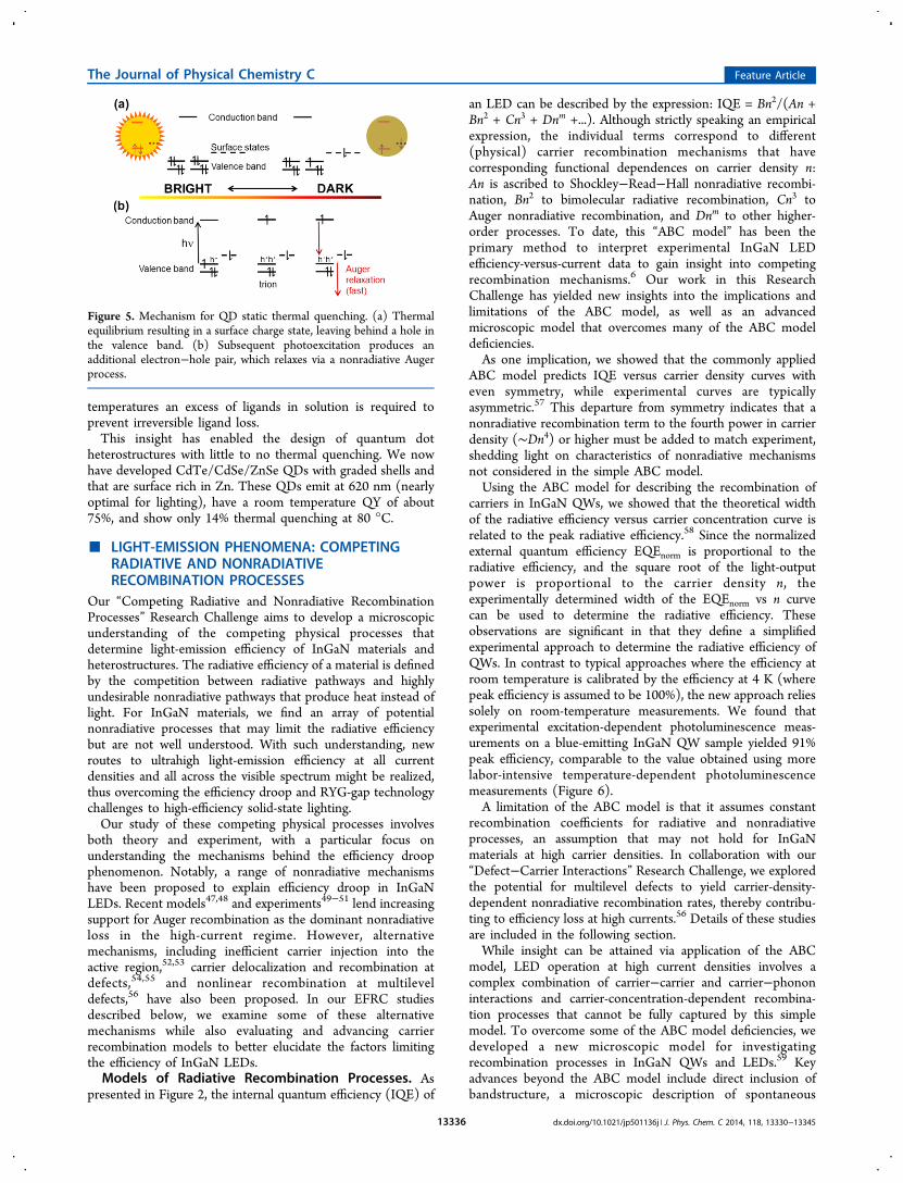
thermal promotion of valence band electrons to emptychalcogenide p orbitals on the particle surfaces (Figure 5a).This thermal promotion leaves a hole in the valence band, sothat subsequent photoexcitation produces a positive trion. Thetrion undergoes relatively rapid nonradiative Auger recombi-nation, rendering the particle dark (Figure 5b).46 Ligands thatbind to empty p orbitals on the particle surfaces minimize staticthermal quenching up to temperatures of ∼80 °C, but at higher
The Journal of Physical Chemistry C Feature Article
dx.doi.org/10.1021/jp501136j | J. Phys. Chem. C 2014, 118, 13330−1334513335
temperatures an excess of ligands in solution is required toprevent irreversible ligand loss.This insight has enabled the design of quantum dot
heterostructures with little to no thermal quenching. We nowhave developed CdTe/CdSe/ZnSe QDs with graded shells andthat are surface rich in Zn. These QDs emit at 620 nm (nearlyoptimal for lighting), have a room temperature QY of about75%, and show only 14% thermal quenching at 80 °C.
■ LIGHT-EMISSION PHENOMENA: COMPETINGRADIATIVE AND NONRADIATIVERECOMBINATION PROCESSES
Our “Competing Radiative and Nonradiative RecombinationProcesses” Research Challenge aims to develop a microscopicunderstanding of the competing physical processes thatdetermine light-emission efficiency of InGaN materials andheterostructures. The radiative efficiency of a material is definedby the competition between radiative pathways and highlyundesirable nonradiative pathways that produce heat instead oflight. For InGaN materials, we find an array of potentialnonradiative processes that may limit the radiative efficiencybut are not well understood. With such understanding, newroutes to ultrahigh light-emission efficiency at all currentdensities and all across the visible spectrum might be realized,thus overcoming the efficiency droop and RYG-gap technologychallenges to high-efficiency solid-state lighting.Our study of these competing physical processes involves
both theory and experiment, with a particular focus onunderstanding the mechanisms behind the efficiency droopphenomenon. Notably, a range of nonradiative mechanismshave been proposed to explain efficiency droop in InGaNLEDs. Recent models47,48 and experiments49−51 lend increasingsupport for Auger recombination as the dominant nonradiativeloss in the high-current regime. However, alternativemechanisms, including inefficient carrier injection into theactive region,52,53 carrier delocalization and recombination atdefects,54,55 and nonlinear recombination at multileveldefects,56 have also been proposed. In our EFRC studiesdescribed below, we examine some of these alternativemechanisms while also evaluating and advancing carrierrecombination models to better elucidate the factors limitingthe efficiency of InGaN LEDs.Models of Radiative Recombination Processes. As
presented in Figure 2, the internal quantum efficiency (IQE) of
an LED can be described by the expression: IQE = Bn2/(An +Bn2 + Cn3 + Dnm +...). Although strictly speaking an empiricalexpression, the individual terms correspond to different(physical) carrier recombination mechanisms that havecorresponding functional dependences on carrier density n:An is ascribed to Shockley−Read−Hall nonradiative recombi-nation, Bn2 to bimolecular radiative recombination, Cn3 toAuger nonradiative recombination, and Dnm to other higher-order processes. To date, this “ABC model” has been theprimary method to interpret experimental InGaN LEDefficiency-versus-current data to gain insight into competingrecombination mechanisms.6 Our work in this ResearchChallenge has yielded new insights into the implications andlimitations of the ABC model, as well as an advancedmicroscopic model that overcomes many of the ABC modeldeficiencies.As one implication, we showed that the commonly applied
ABC model predicts IQE versus carrier density curves witheven symmetry, while experimental curves are typicallyasymmetric.57 This departure from symmetry indicates that anonradiative recombination term to the fourth power in carrierdensity (∼Dn4) or higher must be added to match experiment,shedding light on characteristics of nonradiative mechanismsnot considered in the simple ABC model.Using the ABC model for describing the recombination of
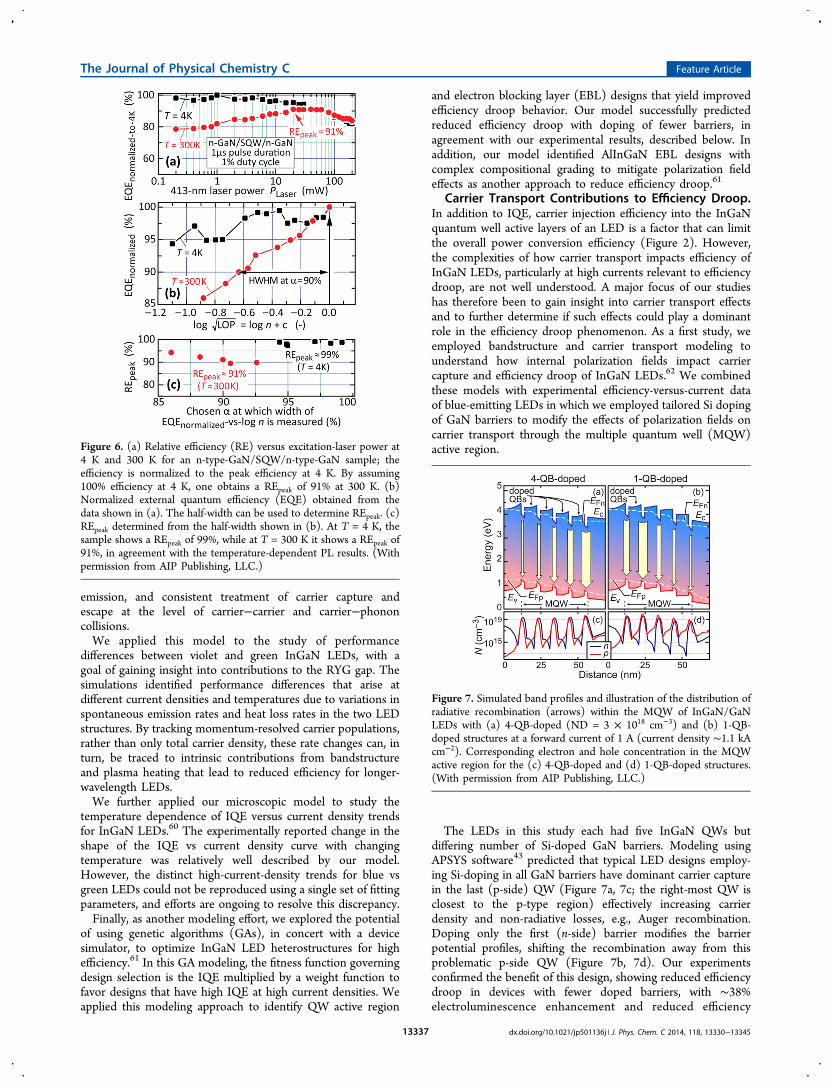
carriers in InGaN QWs, we showed that the theoretical widthof the radiative efficiency versus carrier concentration curve isrelated to the peak radiative efficiency.58 Since the normalizedexternal quantum efficiency EQEnorm is proportional to theradiative efficiency, and the square root of the light-outputpower is proportional to the carrier density n, theexperimentally determined width of the EQEnorm vs n curvecan be used to determine the radiative efficiency. Theseobservations are significant in that they define a simplifiedexperimental approach to determine the radiative efficiency ofQWs. In contrast to typical approaches where the efficiency atroom temperature is calibrated by the efficiency at 4 K (wherepeak efficiency is assumed to be 100%), the new approach reliessolely on room-temperature measurements. We found thatexperimental excitation-dependent photoluminescence meas-urements on a blue-emitting InGaN QW sample yielded 91%peak efficiency, comparable to the value obtained using morelabor-intensive temperature-dependent photoluminescencemeasurements (Figure 6).A limitation of the ABC model is that it assumes constant
recombination coefficients for radiative and nonradiativeprocesses, an assumption that may not hold for InGaNmaterials at high carrier densities. In collaboration with our“Defect−Carrier Interactions” Research Challenge, we exploredthe potential for multilevel defects to yield carrier-density-dependent nonradiative recombination rates, thereby contribu-ting to efficiency loss at high currents.56 Details of these studiesare included in the following section.While insight can be attained via application of the ABC
model, LED operation at high current densities involves acomplex combination of carrier−carrier and carrier−phononinteractions and carrier-concentration-dependent recombina-tion processes that cannot be fully captured by this simplemodel. To overcome some of the ABC model deficiencies, wedeveloped a new microscopic model for investigatingrecombination processes in InGaN QWs and LEDs.59 Keyadvances beyond the ABC model include direct inclusion ofbandstructure, a microscopic description of spontaneous
Figure 5. Mechanism for QD static thermal quenching. (a) Thermalequilibrium resulting in a surface charge state, leaving behind a hole inthe valence band. (b) Subsequent photoexcitation produces anadditional electron−hole pair, which relaxes via a nonradiative Augerprocess.
The Journal of Physical Chemistry C Feature Article
dx.doi.org/10.1021/jp501136j | J. Phys. Chem. C 2014, 118, 13330−1334513336
emission, and consistent treatment of carrier capture andescape at the level of carrier−carrier and carrier−phononcollisions.We applied this model to the study of performance
differences between violet and green InGaN LEDs, with agoal of gaining insight into contributions to the RYG gap. Thesimulations identified performance differences that arise atdifferent current densities and temperatures due to variations inspontaneous emission rates and heat loss rates in the two LEDstructures. By tracking momentum-resolved carrier populations,rather than only total carrier density, these rate changes can, inturn, be traced to intrinsic contributions from bandstructureand plasma heating that lead to reduced efficiency for longer-wavelength LEDs.We further applied our microscopic model to study the
temperature dependence of IQE versus current density trendsfor InGaN LEDs.60 The experimentally reported change in theshape of the IQE vs current density curve with changingtemperature was relatively well described by our model.However, the distinct high-current-density trends for blue vsgreen LEDs could not be reproduced using a single set of fittingparameters, and efforts are ongoing to resolve this discrepancy.Finally, as another modeling effort, we explored the potential
of using genetic algorithms (GAs), in concert with a devicesimulator, to optimize InGaN LED heterostructures for highefficiency.61 In this GA modeling, the fitness function governingdesign selection is the IQE multiplied by a weight function tofavor designs that have high IQE at high current densities. Weapplied this modeling approach to identify QW active region
and electron blocking layer (EBL) designs that yield improvedefficiency droop behavior. Our model successfully predictedreduced efficiency droop with doping of fewer barriers, inagreement with our experimental results, described below. Inaddition, our model identified AlInGaN EBL designs withcomplex compositional grading to mitigate polarization fieldeffects as another approach to reduce efficiency droop.61
Carrier Transport Contributions to Efficiency Droop.In addition to IQE, carrier injection efficiency into the InGaNquantum well active layers of an LED is a factor that can limitthe overall power conversion efficiency (Figure 2). However,the complexities of how carrier transport impacts efficiency ofInGaN LEDs, particularly at high currents relevant to efficiencydroop, are not well understood. A major focus of our studieshas therefore been to gain insight into carrier transport effectsand to further determine if such effects could play a dominantrole in the efficiency droop phenomenon. As a first study, weemployed bandstructure and carrier transport modeling tounderstand how internal polarization fields impact carriercapture and efficiency droop of InGaN LEDs.62 We combinedthese models with experimental efficiency-versus-current dataof blue-emitting LEDs in which we employed tailored Si dopingof GaN barriers to modify the effects of polarization fields oncarrier transport through the multiple quantum well (MQW)active region.
The LEDs in this study each had five InGaN QWs butdiffering number of Si-doped GaN barriers. Modeling usingAPSYS software43 predicted that typical LED designs employ-ing Si-doping in all GaN barriers have dominant carrier capturein the last (p-side) QW (Figure 7a, 7c; the right-most QW isclosest to the p-type region) effectively increasing carrierdensity and non-radiative losses, e.g., Auger recombination.Doping only the first (n-side) barrier modifies the barrierpotential profiles, shifting the recombination away from thisproblematic p-side QW (Figure 7b, 7d). Our experimentsconfirmed the benefit of this design, showing reduced efficiencydroop in devices with fewer doped barriers, with ∼38%electroluminescence enhancement and reduced efficiency
Figure 6. (a) Relative efficiency (RE) versus excitation-laser power at4 K and 300 K for an n-type-GaN/SQW/n-type-GaN sample; theefficiency is normalized to the peak efficiency at 4 K. By assuming100% efficiency at 4 K, one obtains a REpeak of 91% at 300 K. (b)Normalized external quantum efficiency (EQE) obtained from thedata shown in (a). The half-width can be used to determine REpeak. (c)REpeak determined from the half-width shown in (b). At T = 4 K, thesample shows a REpeak of 99%, while at T = 300 K it shows a REpeak of91%, in agreement with the temperature-dependent PL results. (Withpermission from AIP Publishing, LLC.)
Figure 7. Simulated band profiles and illustration of the distribution ofradiative recombination (arrows) within the MQW of InGaN/GaNLEDs with (a) 4-QB-doped (ND = 3 × 1018 cm−3) and (b) 1-QB-doped structures at a forward current of 1 A (current density ∼1.1 kAcm−2). Corresponding electron and hole concentration in the MQWactive region for the (c) 4-QB-doped and (d) 1-QB-doped structures.(With permission from AIP Publishing, LLC.)
The Journal of Physical Chemistry C Feature Article
dx.doi.org/10.1021/jp501136j | J. Phys. Chem. C 2014, 118, 13330−1334513337
droop in the design with one doped barrier vs four dopedbarriers.In addition to strong polarization fields, III−N alloys are
known to have a relatively strong asymmetry in electron andhole concentrations and mobilities. For InGaN LEDs underhigh injection conditions, this asymmetry leads to strongelectron drift into the p-type layer, reducing overall quantumefficiency. Experimental efficiency versus current curves canthen be well described by the inclusion of a drift-inducedleakage term in the ABC recombination model. We showedthat this term has a third- and fourth-order power dependenceon carrier concentration in the active region, where the third-order term, CDL, is estimated to be about 10−29 cm6/s.64
While the efficiency droop phenomenon is largely associatedwith InGaN LEDs, we extended our studies to alternative III−Valloys where carrier transport asymmetry may also play a role.65
Our studies confirmed that efficiency droop is not seen inAlInGaP red LEDs at room temperature. Quite notably,however, we found that efficiency droop is present in theseLEDs at lower temperatures, a trend not predicted for Augerrecombination. This observation was shown to be consistentwith a drift-leakage contribution to efficiency droop, mediatedby asymmetric carrier transport properties. In the case ofAlInGaP, lower temperatures, where this asymmetry isenhanced due to stronger freeze-out of holes compared toelectrons, are required to observe the droop behavior.
■ LIGHT-EMISSION PHENOMENA: DEFECT−CARRIERINTERACTIONS
Among the nonradiative recombination processes just dis-cussed, defect-mediated recombination (associated with the Acoefficient) is one believed to be particularly important, as it ispresent at all InGaN compositions and hence is a key issue forthe RYG gap. Our “Defect−Carrier Interactions” ResearchChallenge thus aims to understand the electrical, optical, andstructural properties of defects in InGaN materials andheterostructures. With such understanding, routes to circum-venting defect contributions to nonradiative carrier recombi-nation might be realized, helping to overcome the blue-efficiency and RYG-gap technology challenges.Our studies have made use of two capabilities, both
continuing to be developed.The first capability is density functional theory, in which we
are attempting to treat atomic configuration changes duringcarrier capture events, and not just with simplified one-dimensional coordinate models but with realistic multidimen-sional configurations.The second capability is deep level optical spectroscopy
(DLOS).66 DLOS is a photocapacitance technique that usessub-bandgap, monochromatic light to stimulate photoemissionfrom deep-level defects located in the depletion region of theLED. The time derivative of the photocapacitance response atthe instant illumination begins is proportional to the deep leveloptical cross-section (σo), which is the fundamental opticalidentifier of a defect state and can be thought of as the opticalabsorbance per unit defect. The optical deep-level energy in thebandgap (Eo) is determined by fitting the dependence of σo onphotoexcitation energy to a theoretical model.67 The defectdensity (Nt) within an individual QW is determined using thePoisson equation and the change in applied voltage (ΔV)required to maintain a fixed depletion depth at the QW upondefect photoemission.
Defects in InGaN QWs. In an initial study, we used DLOSto investigate the potential contribution of defects to the RYGefficiency gap.68 Defects are a likely contributor to this gapbecause achieving longer-wavelength light emission requiresincreased indium incorporation, which in turn often requireslowered QW growth temperature (Tg). The lowered Tg canincrease impurity (extrinsic defect) incorporation, and theincreased strain associated with the higher indium content candrive excess intrinsic defect formation.DLOS of blue- (∼450 nm) and green-emitting (∼530 nm)
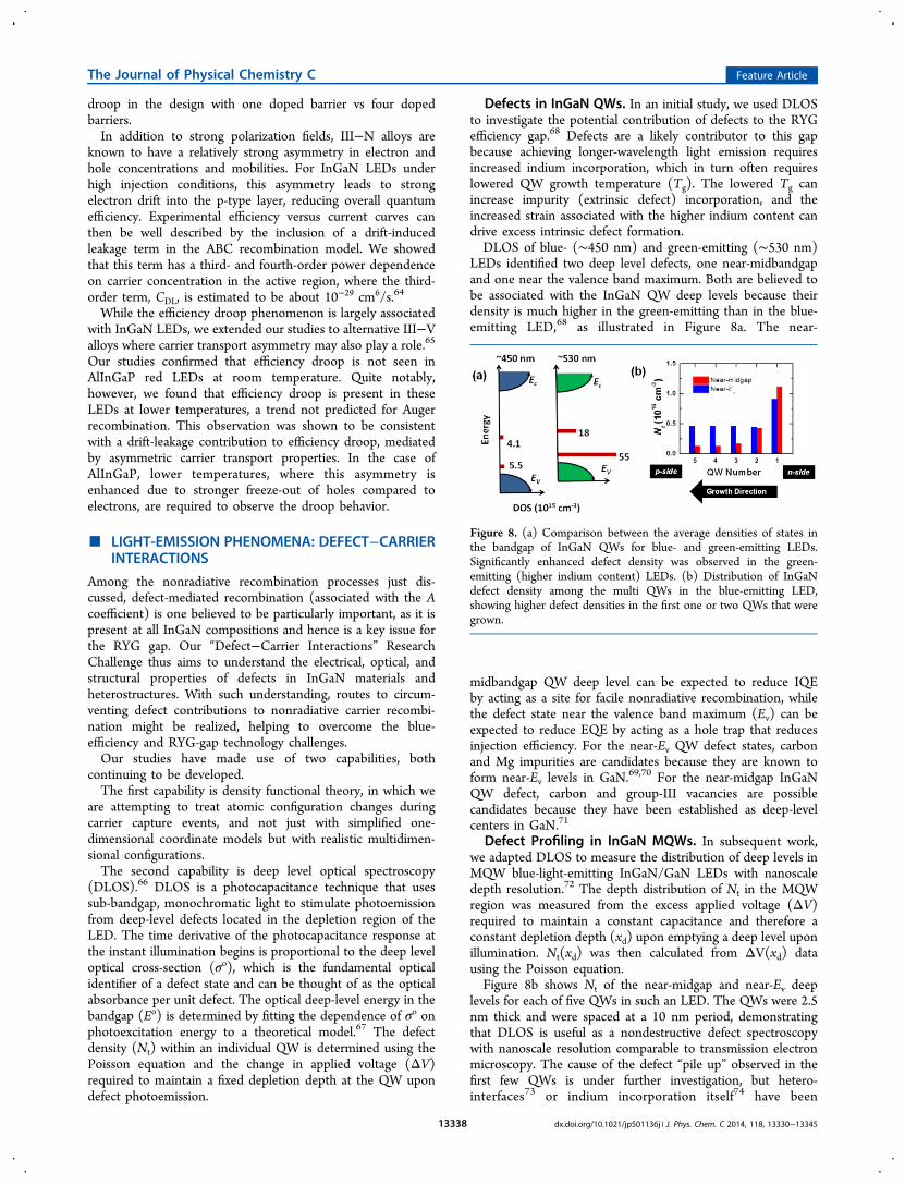
LEDs identified two deep level defects, one near-midbandgapand one near the valence band maximum. Both are believed tobe associated with the InGaN QW deep levels because theirdensity is much higher in the green-emitting than in the blue-emitting LED,68 as illustrated in Figure 8a. The near-
midbandgap QW deep level can be expected to reduce IQEby acting as a site for facile nonradiative recombination, whilethe defect state near the valence band maximum (Ev) can beexpected to reduce EQE by acting as a hole trap that reducesinjection efficiency. For the near-Ev QW defect states, carbonand Mg impurities are candidates because they are known toform near-Ev levels in GaN.69,70 For the near-midgap InGaNQW defect, carbon and group-III vacancies are possiblecandidates because they have been established as deep-levelcenters in GaN.71
Defect Profiling in InGaN MQWs. In subsequent work,we adapted DLOS to measure the distribution of deep levels inMQW blue-light-emitting InGaN/GaN LEDs with nanoscaledepth resolution.72 The depth distribution of Nt in the MQWregion was measured from the excess applied voltage (ΔV)required to maintain a constant capacitance and therefore aconstant depletion depth (xd) upon emptying a deep level uponillumination. Nt(xd) was then calculated from ΔV(xd) datausing the Poisson equation.Figure 8b shows Nt of the near-midgap and near-Ev deep
levels for each of five QWs in such an LED. The QWs were 2.5nm thick and were spaced at a 10 nm period, demonstratingthat DLOS is useful as a nondestructive defect spectroscopywith nanoscale resolution comparable to transmission electronmicroscopy. The cause of the defect “pile up” observed in thefirst few QWs is under further investigation, but hetero-interfaces73 or indium incorporation itself74 have been
Figure 8. (a) Comparison between the average densities of states inthe bandgap of InGaN QWs for blue- and green-emitting LEDs.Significantly enhanced defect density was observed in the green-emitting (higher indium content) LEDs. (b) Distribution of InGaNdefect density among the multi QWs in the blue-emitting LED,showing higher defect densities in the first one or two QWs that weregrown.
The Journal of Physical Chemistry C Feature Article
dx.doi.org/10.1021/jp501136j | J. Phys. Chem. C 2014, 118, 13330−1334513338

suggested to sequester (or getter) defects to the benefit ofsubsequently grown QWs.Multilevel Defects. As mentioned in the previous section
on Competing Radiative and Nonradiative RecombinationProcesses, nonradiative recombination by defects is describedby Shockley−Read−Hall (SRH) theory.75,76A common limiting (and vastly simplified) case of SRH is the
case of defects with only a single electronic level. In this case,the defect-mediated nonradiative recombination rate is linear incarrier density (n), and because other radiative and nonradiativerecombination rates scale as n to higher powers, the relativeimpact of defects on LED efficiency becomes increasingly smallwith increasingly high drive currents and carrier densities.However, in other cases, defects can have multiple electronic
levels.77 Defect-mediated nonradiative recombination in suchcases can be superlinear in current and carrier densities and canthus be a contributor to droop-like behavior in LEDs.56 Inother words, it is possible for defects to influence LEDperformance even at high drive currents, despite the commonassumption otherwise.Defect Cross Sections for Carrier Capture. Computa-
tional studies of defects have typically focused on defect levels,which determine the relative rates of carrier capture andemission at a defect. However, at high carrier concentrations,carrier capture tends to overwhelm carrier emission, and theposition of the defect level within the bandgap becomes lessimportant than the carrier capture cross sections. We havedeveloped procedures to calculate the activation energies thatcontrol carrier capture78,79 both for simplified one-dimensionalcoordinate models and for realistic multidimensional config-urations. Initial application of these models to the galliumvacancy gave results that agree well with experiments.Furthermore, the highest carrier densities and thus the majorityof defect-induced recombination occur in the LED quantumwells.
■ LIGHT-EMISSION PHENOMENA: ENHANCEDSPONTANEOUS EMISSION
In traditional 2D planar quantum-well architectures, sponta-neous emission rates are largely determined by the materialsthemselves. In nanostructured architectures, however, sponta-neous rates can be enhanced. Our “Enhanced SpontaneousEmission” Research Challenge explores ways in whichspontaneous emission can be enhanced through modificationof the environment within which the emission takes place (thePurcell effect80) and therefore ways in which spontaneousemission can better compete with parasitic nonradiative carrierrecombination. If significant enough enhancements can berealized, routes might be developed to overcome the blue-efficiency and RYG-gap technology challenges. In addition, weare investigating routes to enhance quantum dot emission bycoupling to metallic nanoparticles that could also impact thenarrow-line-width red phosphor technology challenge.Our current explorations focus on two nanophotonic
approaches for modifying the emission environment: controlof photonic density of states81,82 (photonic crystals) andintroduction of intense localized electromagnetic fields83−86
(through plasmonics). Both approaches require integration ofemitters with dielectric, plasmonic, or photonic crystal cavities,which we accomplish through nanofabrication and epitaxialgrowth (photonic crystals, fabricated metallic structures),chemical synthetic routes (core−shell dielectric/metallicspheres), or a combination of nanofabricated dielectric
structures and assemblies of emitters (2D photonic crystalsand QDs).
Fully 3D Semiconductor Photonic Crystals. Mostprevious work on visible photonic crystals (PCs) has focused:(a) on materials like titanium dioxide that are transparent in thevisible but with relatively low (n ∼ 2.5) refractive indices thatrestrict the magnitude of photonic crystal effects and (b) on 2Dgeometries that are easier to fabricate but do not offer full 3Dlight control.To overcome these limitations, we have explored a fully 3D
photonic crystal fabricated in Si semiconductor material.87 Sihas the two advantages of: (a) the maturity of the techniqueswith which it can be processing and (b) its high (n ∼ 3.5)refractive index, which enables a large photonic strength (widephotonic bandgap, large photonic density of states).Of course, because Si absorbs in the visible, it would not
normally be considered applicable for SSL. However, we haveexperimentally demonstrated that the practical operationalfrequency range of a silicon-based 3D photonic crystal can beextended nearly into the visible (to about 700 nm), ∼400 nmabove the absorption edge of silicon, due to the slow increase inthe imaginary part of the refractive index (k) with decreasingwavelength. Moreover, we demonstrated that embedded defectstructures in such Si logpile PCs can be used to create cavitymodes within the photonic bandgap, thus paving the way tostudying interactions between emitters in such cavities withartificially tailored photonic densities of states.In subsequent work, we explored a fully 3D photonic crystal
fabricated in GaN semiconductor material,88 as illustrated inFigure 9. This tour-deforce nine-layer logpile 3D photonic
crystal (3DPC) was composed of single-crystalline GaNnanorods ∼100 nm in size grown epitaxially using sequentiallithography and selective-area MOCVD. Optical measurementsalong the stacking direction showed a wide photonic bandgapin the visible (between 380 and 500 nm). The realization ofIII−N-based 3DPCs (and ultimately cavities) opens the door tothe possibility of full 3D control of the spontaneous emissionrate of nitride emitters.87,88
Plasmonic Dipole Nanoantennas. The use of plasmonicantennas in light-emitting semiconductor devices has been
Figure 9. Cross-section SEM image of a nine-layer GaN logpile with a300 nm lattice constant and rod height of 100 nm at lower pressureoptimal growth conditions to enable nucleation on the GaN epilayerresulting in a 2D growth mode. The top right-hand side image showsan enlarged top view, and the bottom image shows an enlarged sectionof the perspective view of regions indicated by a dotted black box. Thewidth of the rod is approximately 135 nm.
The Journal of Physical Chemistry C Feature Article
dx.doi.org/10.1021/jp501136j | J. Phys. Chem. C 2014, 118, 13330−1334513339

extensively explored in recent years. Such antennas enhanceboth radiative recombination within the device as well as theout-coupling of that radiation into free space. In this research,we are exploring the potential of plasmonic antennas forenhancing spontaneous emission from emitters with lower-than-ideal internal quantum efficiency. We are using computa-tional finite-difference time-domain (FDTD) simulations tostudy idealized nanophotonic emitters that are embedded inmaterials with various refractive indices; are coupled to half-dipole Ag antennas with optimized geometries; and emit lightat the four (red, yellow, green, blue) wavelengths of greatestinterest to SSL. The work is in progress, but preliminary resultsindicate that plasmonic antennas have some promise in the red(where Joule losses are lower) but less so in the yellow, green,and blue (where Joule losses are higher).Core−Shell Plasmonic Antennas. An alternative use of
plasmonics is not in electroluminescent structures, as studiedabove, but in photoluminescent structures useful for wave-length downconversion. We have done some exploratory workin core−shell plasmonic geometries, in which the emitter is thecore and the metal is the shell (rather than the more usualopposite configuration). This geometry has many advantages,such as uniformity of the enhanced optical field inside, lack ofpolarization sensitivity, and environmental protection of theemitter. In addition, this core−shell structure is ideal fordecoupling the enhancements of the absorption and emissionprocesses.For a 633 nm dye core surrounded by a Au shell, we find that
the optimal ratio between the shell thickness and the innerradius is approximately 0.3 when the excitation wavelength is632 nm. When this ratio is fixed at the optimal value, largercore radius and shell thickness produce greater intensityenhancement, with total fluorescence enhancements of ∼25possible. The geometry discussed here is well-suited to red rare-earth phosphors used in SSL today, as it promises to greatlyenhance their effective absorption cross section.89
■ LIGHT-EMISSION PHENOMENA: BEYONDSPONTANEOUS EMISSION
Because of nonradiative processes, such as Auger recombina-tion, which become more pronounced at high carrier densities,it is of interest to explore radiative recombination processesthat can outcompete these nonradiative processes. Enhancedspontaneous emission, as discussed in the previous section, isone possibility. Stimulated emission is yet another. Our“Beyond Spontaneous Emission” Research Challenge is focusedon exactly this: exploring the possibility that lasers, based onstimulated emission, can provide a route to high efficiency.Indeed, beyond potentially high efficiency, lasers have otherpossible benefits, including ease of mixing and directing andfocusing of the light. If these benefits could be realized acrossthe visible spectrum, they could provide new routes toovercoming the blue-efficiency, RYG-gap, and enhancedfunctionality SSL technology challenges.However, laser light sources for SSL are in their infancy, and
much work needs to be done to understand both their potentialand their limitations. In this Research Challenge severaldifferent aspects of light generation have been investigatedwhere the common theme is that the light generationmechanism is not the standard spontaneous emission used incommercially available white light LEDs. First, we investigatedthe quality of the white light produced by mixing four differentlaser wavelengths to determine its suitability for general
illumination. Second, we investigated the limits of efficiencyimprovements that are possible using lasers for solid-statelighting. Third, lasing from nanowire structures was inves-tigated since nanowire lasers hold the promise for low-threshold, high-efficiency operation at wavelengths extendingfrom the blue to the red.
Four-Color Laser Illuminant. One of the first issues weaddressed in this Research Challenge was the quality of whitelight produced by mixing four laser beams composed of red,yellow, green, and blue wavelengths. One might anticipate thatwhite light composed of very narrow line width (∼1 nm) laserswould not render colors as well as white light with a broaderspectrum. Thus, even if lasers all across the visible spectrumwere much more efficient and economical than LEDs, theymight not be useful for solid-state lighting.To experimentally investigate this question, we constructed a
four-color laser illuminant,8 composed of commercial lab-gradelasers with wavelengths of 635, 589, 532, and 457 nm. Colormixing optics were then used to create a laser-based white lightsource as illustrated in Figure 10. Side-by-side viewing booths
were set up such that observers could compare scenesilluminated either with commercial white light LEDs,incandescent lamps, or the laser illuminant.The results were that the four-color laser white illuminant
was virtually indistinguishable from state-of-the-art whitereference illuminants. This result can be understood in termsof the broadband nature of the reflectance spectra from mosteveryday objects, as well as the broad wavelength response ofthe cones in the human eye. This study thus showed that whitelight produced using lasers was of high enough quality to beconsidered for solid-state lighting.
Blue Laser Diode versus Blue LED Trade-Offs. As justdiscussed, the ultimate illuminant might be very efficient color-mixed RYGB lasers. However, even without lasers in the red,yellow, and green, a blue laser diode (LD) might also haveadvantages over a blue LED as the pump source in the currentwavelength-downconversion paradigm for SSL. To understandthese advantages, as well as limitations, we performed a detailedand self-consistent analysis of the current states of the art forblue LEDs and LDs, along with the potential of both for futureimprovement.This investigation, together with a detailed economic
analysis, indicates that blue lasers have some compellingadvantages over blue LEDs for SSL.90 Compared to
Figure 10. Schematic of a four-color laser-based white illuminant.Light from four lasers is combined using chromatic bean splitters, thenpasses through multiple ground glass diffusers to eliminate laserspeckle before illuminating test objects. (With permission of TheOptical Society.)
The Journal of Physical Chemistry C Feature Article
dx.doi.org/10.1021/jp501136j | J. Phys. Chem. C 2014, 118, 13330−1334513340

spontaneous emission, stimulated emission is an ultrafastrecombination processso fast that it clamps carrier densitiesabove the lasing threshold, clamps the rates of nonradiativerecombination processes (such as Auger) that depend oncarrier density, and, well above the threshold, easily out-competes these nonradiative recombination processes. Thus,lasers can circumvent efficiency droop associated with parasiticnonradiative recombination. This enables LDs to operate in theregime of much higher input power densities than LEDs, inwhich much higher areal chip costs can be tolerated.However, LDs do have other sources of efficiency loss.
Among these are parasitic resistance loss associated with veryhigh current densities and loss associated with small residualoptical absorption within the laser cavity. There thus appear tobe opportunities for novel (perhaps nanophotonic) laserdesigns that decrease current densities and optical losses viacarrier, mode, and gain engineering.Nanowire Lasers. Nanowires (NWs) also show promise as
a future platform for efficient lasers and light generation.91−93
As described in the “Nanowires” Research Challenge, NWs canbe dislocation free and can have enhanced In incorporation,making them suitable for emission at wavelengths from the blueto the red. Semiconductor nanowires have recently seenapplication as plasmonic nanolasers.94,95 In addition, NWs areattractive candidates for efficiency and compactness, being ableto simultaneously function as a standalone optical cavity andgain medium. Furthermore, with the appropriate geometry andlattice spacing, an array of nanowires can behave as a photoniccrystal.96,97 For particular designs, lasers can be realized.In our work, we have explored lasing of single NWs as well as
arrays of NWs, thus far all via optical pumping.For our single-NW lasers, the GaN NW forms the optical
cavity with facets on each end of the wire, as well as providingthe gain medium. Although not obviously of central importancefor SSL, single-mode behavior is of interest for many otherapplications, and so we have explored some of the conditionsfor such single-mode behavior. We find that, for smaller NWs,single-mode operation is preserved far above the lasingthreshold.18 For larger nanowires, multimode operation occurs,so alternate methods for achieving single-mode lasing areneeded.One method for achieving single-mode operation is to place
(using nanoprobe manipulation) two NWs of different lengths,which individually exhibit multimode behavior, side-by-side inclose proximity to form a coupled cavity.98 The couplingbetween the nanowire pair provides a mode selectionmechanism through the Vernier effect and generates stablesingle-mode operation. Another method for achieving single-mode operation was to simply place the NW onto a gold film.99
Due to the mode-dependent losses induced by the goldsubstrate, only a single transverse mode has a loss low enoughto be overcome by the laser gain, thus enabling single-modebehavior. The observed increase in lasing threshold of only∼13% after placement onto gold indicates that the impact ofmetal contacts on the optoelectronic properties is modest.For arrays of NWs, we have explored the use of 2D NW
photonic crystals (2DPCs) to provide lateral feedback forlasing. Because the wavelength at which lateral feedback occursis determined by the photonic crystal geometry, lasers ofdifferent wavelengths can be fabricated on a single chip.Moreover, due to the relatively broad gain bandwidth of III−nitride quantum wells and the lateral nature of the feedback, thewavelength tuning range of the lasers can be quite large: a
remarkable 60 nm of wavelength tuning was demonstrated on asingle chip from a single epitaxial growth.100
■ SUMMARYSolid-state lighting is an emerging technology that has madeenormous progress this past decade and that has much roomfor further progress. The Energy Frontier Research Center forSolid-State Lighting Science aims (a) to help advance thescientific understanding of materials architectures and light-emission phenomena used in the current state-of-the-art solid-state lighting and (b) to explore new materials architectures andlight-emission phenomena with the potential for dramaticimprovements in electricity-to-light conversion efficiency. Todo this, the SSLS EFRC is organized around six ResearchChallenges, two focused on materials architectures and fourfocused on light-emission phenomena.In the EFRC’s two materials architecture Research
Challenges, among the most significant advances have beenthe following.First, methods have been developed for combined bottom-
up, top-down nanofabrication of large-area, uniform arrays ofstraight and smooth III−N nanowires into which axialheterostructures can be embedded and onto which coaxialstructures can also be grown. These methods, particularly whenaided by atomic-scale nanocharacterization and computationalsimulation of synthesis and optoelectronic properties, havemuch potential to enable 3D tailored nano- and mesomaterialsarchitectures that can fill the RYG gap.Second, a new class of Eu3+ phosphor with absorption in the
blue and narrow emission in the red has been developed, andthe dominant mechanism for the well-known but previouslypoorly understood thermal quenching in II−VI quantum dotshas been elucidated. Both of these advances may help enablenew generations of wavelength downconversion materials thatcan solve the deep-red spillover wavelength-downconversionchallenge.In the EFRC’s four light-emission phenomena Research
Challenges, among the most significant advances have been thefollowing.First, “beyond ABC” microscopic models of carrier
recombination have been developed that include many-bodycarrier interactions, carrier transport, strain and polarizationfields, Auger recombination, and defects in both quantum wellsand quantum barriers. These models complicate but alsoprovide a more nuanced view of the physical processes that cancompete with each other for carrier recombination.Second, deep-level optical spectroscopy techniques were
developed that can quantify defect densities in individualInGaN quantum wells, and models were developed thatindicate that point defects with multiple charge levels canlead to recombination rates that are highly nonlinear withcarrier concentration and that can be a contributor to efficiencydroop.Third, a fully 3D photonic crystal was fabricated in GaN
semiconductor material, opening the door to the possibility offull 3D enhancement and control of the spontaneous emissionrate of nitride emitters, perhaps enabling spontaneous emissionto outcompete parasitic nonradiative recombination processes.Fourth, through detailed simulations and human factors
studies, lasers have been identified as a promising alternative toLEDs for solid-state lighting, both as a blue or UV pump forwavelength downconversion, as well as for RYGB color mixing.This paves the way for more serious efforts to understand the
The Journal of Physical Chemistry C Feature Article
dx.doi.org/10.1021/jp501136j | J. Phys. Chem. C 2014, 118, 13330−1334513341

limits to efficiency of both LEDs and lasers as well asarchitectures at the boundary between LEDs and lasers.
■ AUTHOR INFORMATION
Corresponding Author*Phone: 505-844-7843. E-mail: [email protected].
Author ContributionsThe manuscript was written through contributions of allauthors.
NotesThe authors declare no competing financial interest.Biographies
Michael E. Coltrin is Director of the Energy Frontier Research Centerfor Solid-State Lighting Science and a Distinguished Member ofTechnical Staff (DMTS) at Sandia National Laboratories. His researchfocuses on kinetics and morphology evolution in the growth ofsemiconductor materials. He received his PhD in Physical Chemistryfrom the University of Illinois at Urbana.
Andrew M. Armstrong is a Principal Member of Technical Staff(PMTS) at Sandia National Laboratories. His research is centered ondevelopment and application of deep-level optical spectroscopy of III−nitride materials. He received his PhD in Electrical and ComputerEngineering from Ohio State University.
Igal Brener is a DMTS at Sandia National Laboratories. His researchdeals with fundamental and applied aspects of metamaterials,plasmonics, and other nanophotonics phenomena. He received hisPhD in Physics from Technion, Haifa, Israel.
Weng W. Chow is a DMTS at Sandia National Laboratories, where hisprimary research involves applying microscopic theory to semi-conductor laser development. He received his PhD in Physics from theUniversity of Arizona.
Mary H. Crawford is a Senior Scientist at Sandia NationalLaboratories. Her research interests are currently centered onnitride-based materials and optoelectronic devices. She received herPhD in Physics from Brown University.
Arthur J. Fischer is a PMTS at Sandia National Laboratories,conducting research on emission physics and optical characterizationof nitride-semiconductor materials and devices. He received his PhD inPhysics from Oklahoma State University.
David F. Kelley is Professor and Founding Faculty in the Chemistryand Chemical Biology Department at the University of California,Merced. His research group uses ultrafast optical spectroscopy toexamine the optical and electronic properties of semiconductingnanoparticles. He received his PhD in Physical Chemistry from theUniversity of Washington.
Daniel D. Koleske is a PMTS at Sandia National Laboratories. Hisresearch includes MOCVD growth of nitride semiconductors for SSL,with interest in growth kinetics and morphology evolution. Hereceived his PhD in Physical Chemistry from the University ofChicago.
Lincoln J. Lauhon is Professor and Associate Chair of the Departmentof Materials Science and Engineering at Northwestern University. Hisresearch group pursues advances in the synthesis and characterizationof new nanostructured materials. He received his PhD in Physics fromCornell University.
James E. Martin is a DMTS at Sandia National Laboratories. Hisresearch interests include investigations of the recombinationdynamics and luminescence of quantum dots and nanophosphors.
He received his PhD in Physical Chemistry from the University ofWashington.
May Nyman is Associate Professor in the Department of Chemistry atOregon State University. Her research interests include inorganic ionexchangers, niobates and tantalates, luminescent materials, andinorganic polyanions and polycations. She received her PhD inChemistry from the University of New Mexico.
E. Fred Schubert is Wellfleet Senior Constellation Professor of theFuture Chips Constellation with appointments in the ElectricalEngineering and Physics Departments at Rensselaer PolytechnicInstitute. His primary research interest is in the field of compoundsemiconductor materials and devices. He received his PhD in ElectricalEngineering at the University of Stuttgart.
Lauren E. Shea-Rohwer is a PMTS at Sandia National Laboratories.Her research currently includes phosphor powders and films andnanoscale luminescent materials such as II−VI quantum dots. Shereceived her PhD in Materials Science from the University ofCalifornia at San Diego.
Ganapathi Subramania is a PMTS at Sandia National Laboratories.His research interest involves exploring light−matter interaction insidenanostructured environments like photonic crystals and metamaterials.He received his PhD in Electrical Engineering and Applied Physicsfrom Iowa State University.
Jeffrey Y. Tsao is Chief Scientist of the Energy Frontier ResearchCenter for Solid-State Lighting Science and a DMTS at SandiaNational Laboratories. His research involves integrated science,technology, and economic modeling in solid-state lighting and otherareas. He received his PhD in Applied Physics from HarvardUniversity.
George T. Wang is a PMTS at Sandia National Laboratories. Hisprimary research efforts focus on the synthesis, characterization, andapplications of III−nitride nanowires grown by MOCVD. He receivedhis PhD in Chemical Engineering from Stanford University.
Jonathan J. Wierer, Jr. is a PMTS at Sandia National Laboratories,where he conducts research on III−nitride material properties anddeveloping novel optoelectronic devices. He received his PhD inElectrical Engineering from the University of Illinois at Urbana.
Jeremy B. Wright is a graduate student at the University of NewMexico’s Center for High Technology Materials, the University ofNew Mexico, and Sandia National Laboratories. His work focuses onoptoelectronic properties of novel III−nitride nanostructures.
■ ACKNOWLEDGMENTSThis work was supported by Sandia’s Solid-State LightingScience Energy Frontier Research Center, sponsored by theDepartment of Energy Office of Basic Energy Science. SandiaNational Laboratories is a multiprogram laboratory managedand operated by Sandia Corporation, a wholly ownedsubsidiary of Lockheed Martin Company, for the United StatesDepartment of Energy’s National Nuclear Security Admin-istration under Contract DE-AC04-94AL85000.
■ REFERENCES(1) Tsao, J. Y.; Waide, P. The World’s Appetite for Light: EmpiricalData and Trends Spanning Three Centuries and Six Continents.Leukos 2010, 6, 259−281.(2) Solid-State Lighting Research and Development Multi-Year ProgramPlan; April, 2013, 2013.(3) Crawford, M. H.; Wierer, J. J.; Fischer, A. J.; Wang, G. T.;Koleske, D. D.; Subramania, G.; Coltrin, M. E.; Tsao, J. Y.; Karlicek, R.
The Journal of Physical Chemistry C Feature Article
dx.doi.org/10.1021/jp501136j | J. Phys. Chem. C 2014, 118, 13330−1334513342

F. Solid-State Lighting: Toward Smart and Ultra-Efficient Materials,Devices, Lamps and Systems. In Photonics: Photonics Technology andInstrumentation, Andrews, D. L., Ed. Wiley: New York, 2014; Vol. 3.(4) Tsao, J. Y.; Coltrin, M. E.; Crawford, M. H.; Simmons, J. A. Solid-State Lighting: An Integrated Human Factors, Technology, andEconomic Perspective. Proc. IEEE 2010, 98, 1162−1179.(5) Narukawa, Y.; Ichikawa, M.; Sanga, D.; Sano, M.; Mukai, T.White Light Emitting Diodes with Super-High Luminous Efficacy. J.Phys. D: Appl. Phys. 2010, 43, 354002.(6) Piprek, J. Efficiency Droop in Nitride-Based Light-EmittingDiodes. Phys. Status Solidi (a) 2010, 207, 2217−2225.(7) Phillips, J. M.; Coltrin, M. E.; Crawford, M. H.; Fischer, A. J.;Krames, M. R.; Mueller-Mach, R.; Mueller, G. O.; Ohno, Y.; Rohwer,L. E.; Simmons, J. A. Research Challenges to Ultra-Efficient InorganicSolid-State Lighting. Laser Photonics Rev. 2007, 1, 307−333.(8) Neumann, A.; Wierer, J. J., Jr.; Davis, W.; Ohno, Y.; Brueck, S. R.J.; Tsao, J. Y. Four-Color Laser White Illuminant Demonstrating HighColor-Rendering Quality. Opt. Express 2011, 19, A982−A990.(9) Schubert, E. F.; Kim, J. K. Solid-State Light Sources GettingSmart. Science 2005, 308, 1274−1278.(10) Yan, R.; Gargas, D.; Yang, P. Nanowire Photonics. Nat.Photonics 2009, 3, 569−576.(11) Li, S.; Waag, A. GaN Based Nanorods for Solid State Lighting. J.Appl. Phys. 2012, 111, 071101.(12) Duan, X.; Lieber, C. M. Laser-Assisted Catalytic Growth ofSingle Crystal GaN Nanowires. J. Am. Chem. Soc. 2000, 122, 188−189.(13) Kuykendall, T.; Pauzauskie, P.; Lee, S.; Zhang, Y.; Goldberger,J.; Yang, P. Metalorganic Chemical Vapor Deposition Route to GaNNanowires with Triangular Cross Sections. Nano Lett. 2003, 3, 1063−1066.(14) Hersee, S. D.; Sun, X.; Wang, X. The Controlled Growth ofGaN Nanowires. Nano Lett. 2006, 6, 1808−1811.(15) Li, Q.; Wang, G. T. Improvement in Aligned GaN NanowireGrowth Using Submonolayer Ni Catalyst Films. Appl. Phys. Lett. 2008,93, 043119−043119−3.(16) Wang, G. T.; Talin, A. A.; Werder, D. J.; Creighton, J. R.; Lai, E.;Anderson, R. J.; Arslan, I. Highly Aligned, Template-Free Growth andCharacterization of Vertical GaN Nanowires on Sapphire by Metal−Organic Chemical Vapour Deposition. Nanotechnology 2006, 17, 5773.(17) Wagner, R.; Ellis, W. Vapor-Liquid-Solid Mechanism of SingleCrystal Growth. Appl. Phys. Lett. 1964, 4, 89−90.(18) Li, Q.; Wright, J. B.; Chow, W. W.; Luk, T. S.; Brener, I.; Lester,L. F.; Wang, G. T. Single-Mode GaN Nanowire Lasers. Opt. Express2012, 20, 17873−17879.(19) Li, Q.; Westlake, K. R.; Crawford, M. H.; Lee, S. R.; Koleske, D.D.; Figiel, J. J.; Cross, K. C.; Fathololoumi, S.; Mi, Z.; Wang, G. T.Optical Performance of Top-Down Fabricated InGaN/GaN NanorodLight Emitting Diode Arrays. Opt. Express 2011, 19, 25528−25534.(20) Baird, L.; Ong, C. P.; Cole, R. A.; Haegel, N. M.; Talin, A. A.; Li,Q.; Wang, G. T. Transport Imaging for Contact-Free Measurements ofMinority Carrier Diffusion in GaN, GaN/AlGaN, and GaN/InGaNCore-Shell Nanowires. Appl. Phys. Lett. 2011, 98, 132104.(21) Huang, J. Y.; Zheng, H.; Mao, S. X.; Li, Q.; Wang, G. T. In SituNanomechanics of GaN Nanowires. Nano Lett. 2011, 11, 1618−1622.(22) Greer, J. R.; Nix, W. D. Nanoscale Gold Pillars StrengthenedThrough Dislocation Starvation. Phys. Rev. B 2006, 73, 245410.(23) Shan, Z.; Mishra, R. K.; Asif, S. S.; Warren, O. L.; Minor, A. M.Mechanical Annealing and Source-Limited Deformation in Submicro-metre-Diameter Ni Crystals. Nat. Mater. 2007, 7, 115−119.(24) Uchic, M. D.; Dimiduk, D. M.; Florando, J. N.; Nix, W. D.Sample Dimensions Influence Strength and Crystal Plasticity. Science2004, 305, 986−989.(25) Volkert, C. A.; Lilleodden, E. T. Size Effects in the Deformationof Sub-Micron Au Columns. Philos. Mag. 2006, 86, 5567−5579.(26) Zhu, T.; Li, J. Ultra-Strength Materials. Prog. Mater. Sci. 2010,55, 710−757.(27) Greer, J. R.; De Hosson, J. T. M. Plasticity in Small-SizedMetallic Systems: Intrinsic Versus Extrinsic Size Effect. Prog. Mater. Sci.2011, 56, 654−724.
(28) Li, Q.; Wang, G. T. Strain Influenced Indium CompositionDistribution in GaN/InGaN Core-Shell Nanowires. Appl. Phys. Lett.2010, 97, 181107.(29) Mukai, T.; Yamada, M.; Nakamura, S. In InGaN-Based Uv/Blue/Green/Amber LEDs, Optoelectronics’ 99-Integrated OptoelectronicDevices; International Society for Optics and Photonics: Washington,1999; pp 2−13.(30) Pereira, S.; Correia, M.; Pereira, E.; O’Donnell, K.; Trager-Cowan, C.; Sweeney, F.; Alves, E. Compositional Pulling Effects inin(X)Ga(1-X)N/GaN Layers: A Combined Depth-Resolved Cath-odoluminescence and Rutherford Backscattering/Channeling Study.Phys. Rev. B 2001, 64, 205311.(31) Wong, B. M.; Leonard, F.; Li, Q.; Wang, G. T. Nanoscale Effectson Heterojunction Electron Gases in GaN/AlGaN Core/ShellNanowires. Nano Lett. 2011, 11, 3074−3079.(32) Wang, C.-Y.; Chen, L.-Y.; Chen, C.-P.; Cheng, Y.-W.; Ke, M.-Y.;Hsieh, M.-Y.; Wu, H.-M.; Peng, L.-H.; Huang, J. GaN Nanorod LightEmitting Diode Arrays with a Nearly Constant ElectroluminescentPeak Wavelength. Opt. Express 2008, 16, 10549−10556.(33) Wierer, J. J., Jr.; Li, Q.; Koleske, D. D.; Lee, S. R.; Wang, G. T.III- Nitride Core-Shell Nanowire Arrayed Solar Cells. Nanotechnology2012, 23, 194007.(34) Wang, G. T.; Li, Q.; Wierer, J. J.; Koleske, D. D.; Figiel, J. J.Top−Down Fabrication and Characterization of Axial and Radial III-Nitride Nanowire LEDs. Phys. Status Solidi (a) 2014, 211, 748−751.(35) Riley, J. R.; Padalkar, S.; Li, Q.; Lu, P.; Koleske, D. D.; Wierer, J.J.; Wang, G. T.; Lauhon, L. J. Three-Dimensional Mapping ofQuantum Wells in a GaN/InGaN Core−Shell Nanowire Light-Emitting Diode Array. Nano Lett. 2013, 13, 4317−4325.(36) Riley, J. R.; Bernal, R. A.; Li, Q.; Espinosa, H. D.; Wang, G. T.;Lauhon, L. J. Atom Probe Tomography of a-Axis GaN Nanowires:Analysis of Nonstoichiometric Evaporation Behavior. ACS Nano 2012,6, 3898−3906.(37) Nyman, M.; Rodriguez, M. A.; Shea-Rohwer, L. E.; Martin, J. E.;Provencio, P. P. Highly Versatile Rare Earth Tantalate PyrochloreNanophosphors. J. Am. Chem. Soc. 2009, 131, 11652−11653.(38) Francis, L. T.; Rao, P. P.; Thomas, M.; Mahesh, S.; Reshmi, V.;Thampi, V. D. New Orange-Red Emitting Phosphor La3NbO7: Eu3+Under Blue Excitation. Mater. Lett. 2012, 81, 142−144.(39) Dutta, P.; Khanna, A. Eu3+ Activated Molybdate and TungstateBased Red Phosphors with Charge Transfer Band in Blue Region. ECSJ. Solid State Sci. Technol. 2013, 2, R3153−R3167.(40) Nyman, M.; Rodriguez, M. A.; Rohwer, L. E.; Martin, J. E.;Waller, M.; Osterloh, F. E. Unique LaTaO4 Polymorph for MultipleEnergy Applications. Chem. Mater. 2009, 21, 4731−4737.(41) Bleier, G. C.; Nyman, M.; Rohwer, L. E. S.; Rodriguez, M. A.Seeking the Optimal LaTaO4:Eu Phosphor. J. Solid State Chem. 2011,184, 3221−3227.(42) Li, J. J.; Wang, Y. A.; Guo, W.; Keay, J. C.; Mishima, T. D.;Johnson, M. B.; Peng, X. Large-Scale Synthesis of NearlyMonodisperse Cdse/Cds Core/Shell Nanocrystals Using Air-StableReagents Via Successive Ion Layer Adsorption and Reaction. J. Am.Chem. Soc. 2003, 125, 12567−12575.(43) Xie, R.; Kolb, U.; Li, J.; Basche,́ T.; Mews, A. Synthesis andCharacterization of Highly Luminescent Cdse-Core Cds/Zn0. 5cd0.5s/Zns Multishell Nanocrystals. J. Am. Chem. Soc. 2005, 127, 7480−7488.(44) Shea-Rohwer, L. E.; Martin, J. E.; Cai, X.; Kelley, D. F. Red-Emitting Quantum Dots for Solid-State Lighting. ECS J. Solid State Sci.Technol. 2013, 2, R3112−R3118.(45) Zhao, Y.; Riemersma, C.; Pietra, F.; Koole, R.; de Mello Donega,́C.; Meijerink, A. High-Temperature Luminescence Quenching ofColloidal Quantum Dots. ACS Nano 2012, 6, 9058−9067.(46) Cai, X.; Martin, J. E.; Shea-Rohwer, L. E.; Gong, K.; Kelley, D. F.Thermal Quenching Mechanisms in II-VI Semiconductor Nanocryst-als. J. Phys. Chem. C 2013, 117, 7902−7913.(47) Kioupakis, E.; Rinke, P.; Delaney, K. T.; Van de Walle, C. G.Indirect Auger Recombination as a Cause of Efficiency Droop inNitride Light-Emitting Diodes. Appl. Phys. Lett. 2011, 98, 161107.
The Journal of Physical Chemistry C Feature Article
dx.doi.org/10.1021/jp501136j | J. Phys. Chem. C 2014, 118, 13330−1334513343

(48) Vaxenburg, R.; Rodina, A.; Lifshitz, E.; Efros, A. L. The Role ofPolarization Fields in Auger-Induced Efficiency Droop in Nitride-Based Light-Emitting Diodes. Appl. Phys. Lett. 2013, 103, 221111.(49) Shen, Y.; Mueller, G.; Watanabe, S.; Gardner, N.; Munkholm,A.; Krames, M. Auger Recombination in InGaN Measured byPhotoluminescence. Appl. Phys. Lett. 2007, 91, 141101.(50) Iveland, J.; Martinelli, L.; Peretti, J.; Speck, J. S.; Weisbuch, C.Direct Measurement of Auger Electrons Emitted from a Semi-conductor Light-Emitting Diode Under Electrical Injection: Identi-fication of the Dominant Mechanism for Efficiency Droop. Phys. Rev.Lett. 2013, 110, 177406.(51) Binder, M.; Nirschl, A.; Zeisel, R.; Hager, T.; Lugauer, H.-J.;Sabathil, M.; Bougeard, D.; Wagner, J.; Galler, B. Identification of Nnpand Npp Auger Recombination as Significant Contributor to theEfficiency Droop in (Gain) N Quantum Wells by Visualization of HotCarriers in Photoluminescence. Appl. Phys. Lett. 2013, 103, 071108.(52) Kim, M.-H.; Schubert, M. F.; Dai, Q.; Kim, J. K.; Schubert, E. F.;Piprek, J.; Park, Y. Origin of Efficiency Droop in GaN-Based Light-Emitting Diodes. Appl. Phys. Lett. 2007, 91, 183507.(53) Meyaard, D. S.; Lin, G.-B.; Cho, J.; Schubert, E. F.; Shim, H.;Han, S.-H.; Kim, M.-H.; Sone, C.; Kim, Y. S. Identifying the Cause ofthe Efficiency Droop in GaInN Light-Emitting Diodes by Correlatingthe Onset of High Injection with the Onset of the Efficiency Droop.Appl. Phys. Lett. 2013, 102, 251114.(54) Hader, J.; Moloney, J.; Koch, S. Density-Activated DefectRecombination as a Possible Explanation for the Efficiency Droop inGaN-Based Diodes. J. Appl. Phys. 2010, 96, 221106.(55) Hammersley, S.; Watson-Parris, D.; Dawson, P.; Godfrey, M.;Badcock, T.; Kappers, M.; McAleese, C.; Oliver, R.; Humphreys, C.The Consequences of High Injected Carrier Densities on CarrierLocalization and Efficiency Droop in InGaN/GaN Quantum WellStructures. J. Appl. Phys. 2012, 111, 083512.(56) Modine, N. A.; Armstrong, A. M.; Crawford, M. H.; Chow, W.W. Highly Nonlinear Defect-Induced Carrier Recombination Rates inSemiconductors. J. Appl. Phys. 2013, 114, 144502.(57) Dai, Q.; Shan, Q.; Cho, J.; Schubert, E. F.; Crawford, M. H.;Koleske, D. D.; Kim, M.-H.; Park, Y. On the Symmetry of Efficiency-Versus-Carrier-Concentration Curves in GaInN/GaN Light-EmittingDiodes and Relation to Droop-Causing Mechanisms. Appl. Phys. Lett.2011, 98, 033506.(58) Lin, G.-B.; Shan, Q.; Birkel, A. J.; Cho, J.; Schubert, E. F.;Crawford, M. H.; Westlake, K. R.; Koleske, D. D. Method forDetermining the Radiative Efficiency of GaInN Quantum Wells Basedon the Width of Efficiency-Versus-Carrier-Concentration Curve. Appl.Phys. Lett. 2012, 101, 241104.(59) Chow, W. W.; Crawford, M. H.; Tsao, J. Y.; Kneissl, M. InternalEfficiency of InGaN Light-Emitting Diodes: Beyond a Quasiequili-brium Model. Appl. Phys. Lett. 2010, 97, 121105.(60) Chow, W. W. Modeling of Temperature and ExcitationDependences of Efficiency in an InGaN Light-Emitting Diode. Opt.Express 2014, 22, 1413−1425.(61) Zhu, D.; Schubert, M. F.; Cho, J.; Schubert, E. F.; Crawford, M.H.; Koleske, D. D.; Shim, H.; Sone, C. Genetic Algorithm forInnovative Device Designs in High-Efficiency III-V Nitride Light-Emitting Diodes. Appl. Phys. Express 2012, 5, 012102.(62) Zhu, D.; Noemaun, A. N.; Schubert, M. F.; Cho, J.; Schubert, E.F.; Crawford, M. H.; Koleske, D. D. Enhanced Electron Capture andSymmetrized Carrier Distribution in GaInN Light-Emitting DiodesHaving Tailored Barrier Doping. Appl. Phys. Lett. 2010, 96, 121110.(63) Crosslight Software. www.crosslight.com (accessed April 30,2014).(64) Lin, G.-B.; Meyaard, D.; Cho, J.; Schubert, E. F.; Shim, H.; Sone,C. Analytic Model for the Efficiency Droop in Semiconductors withAsymmetric Carrier-Transport Properties Based on Drift-InducedReduction of Injection Efficiency. Appl. Phys. Lett. 2012, 100, 161106.(65) Shim, J.-I.; Han, D.-P.; Kim, H.; Shin, D.-S.; Lin, G.-B.;Meyaard, D. S.; Shan, Q.; Cho, J.; Schubert, E. F.; Shim, H.; et al.Efficiency Droop in AlGaInP and GaInN Light-Emitting Diodes. Appl.Phys. Lett. 2012, 100, 111106.
(66) Chantre, A.; Vincent, G.; Bois, D. Deep-Level OpticalSpectroscopy in GaAs. Phys. Rev. B 1981, 23, 5335.(67) Passler, R. Photoionization Cross-Section Analysis for a DeepTrap Contributing to Current Collapse in GaN Field-EffectTransistors. J. Appl. Phys. 2004, 96, 715−722.(68) Armstrong, A.; Crawford, M. H.; Koleske, D. D. Contribution ofDeep-Level Defects to Decreasing Radiative Efficiency of InGaN/GaNQuantum Wells with Increasing Emission Wavelength. Appl. Phys.Express 2014, 7, 032101.(69) Hierro, A.; Kwon, D.; Ringel, S.; Hansen, M.; Speck, J.; Mishra,U.; DenBaars, S. Optically and Thermally Detected Deep Levels in N-Type Schottky and P±N GaN Diodes. Appl. Phys. Lett. 2000, 76,3064−3066.(70) Armstrong, A.; Poblenz, C.; Green, D.; Mishra, U.; Speck, J.;Ringel, S. Impact of Substrate Temperature on the Incorporation ofCarbon-Related Defects and Mechanism for Semi-Insulating Behaviorin GaN Grown by Molecular Beam Epitaxy. Appl. Phys. Lett. 2006, 88,082114.(71) Seager, C.; Wright, A.; Yu, J.; Gotz, W. Role of Carbon in GaN.J. Appl. Phys. 2002, 92, 6553−6560.(72) Armstrong, A.; Henry, T. A.; Koleske, D. D.; Crawford, M. H.;Lee, S. R. Quantitative and Depth-Resolved Deep Level DefectDistributions in InGaN/GaN Light Emitting Diodes. Opt. Express2012, 20, A812−A821.(73) Petroff, P.; Miller, R.; Gossard, A.; Wiegmann, W. ImpurityTrapping, Interface Structure, and Luminescence of GaAs QuantumWells Grown by Molecular Beam Epitaxy. Appl. Phys. Lett. 1984, 44,217−219.(74) Akasaka, T.; Gotoh, H.; Saito, T.; Makimoto, T. HighLuminescent Efficiency of InGaN Multiple Quantum Wells Grownon InGaN Underlying Layers. Appl. Phys. Lett. 2004, 85, 3089−3091.(75) Shockley, W.; Read, W., Jr. Statistics of the Recombinations ofHoles and Electrons. Phys. Rev. 1952, 87, 835.(76) Hall, R. Germanium Rectifier Characteristics. Phys. Rev. 1951,83, 228.(77) Sah, C.-T.; Shockley, W. Electron-Hole RecombinationStatistics in Semiconductors Through Flaws with Many ChargeConditions. Phys. Rev. 1958, 109, 1103.(78) Lang, D.; Henry, C. Nonradiative Recombination at DeepLevels in GaAs and Gap by Lattice-Relaxation Multiphonon Emission.Phys. Rev. Lett. 1975, 35, 1525−1528.(79) Henry, C.; Lang, D. V. Nonradiative Capture and Recombina-tion by Multiphonon Emission in GaAs and Gap. Phys. Rev. B 1977,15, 989.(80) Purcell, E. M. Spontaneous Emission Probabilities at RadioFrequencies. Phys. Rev. 1946, 69, 681−681.(81) Boroditsky, M.; Vrijen, R.; Krauss, T. F.; Coccioli, R.; Bhat, R.;Yablonovitch, E. Spontaneous Emission Extraction and PurcellEnhancement from Thin-Film 2-D Photonic Crystals. J. LightwaveTechnol. 1999, 17, 2096−2112.(82) Noda, S.; Fujita, M.; Asano, T. Spontaneous-Emission Controlby Photonic Crystals and Nanocavities. Nat. Photonics 2007, 1, 449−458.(83) Russell, K. J.; Liu, T.-L.; Cui, S.; Hu, E. L. Large SpontaneousEmission Enhancement in Plasmonic Nanocavities. Nat. Photonics2012, 6, 459−462.(84) Sorger, V. J.; Pholchai, N.; Cubukcu, E.; Oulton, R. F.; Kolchin,P.; Borschel, C.; Gnauck, M.; Ronning, C.; Zhang, X. StronglyEnhanced Molecular Fluorescence Inside a Nanoscale Waveguide Gap.Nano Lett. 2011, 11, 4907−4911.(85) Cho, C.-H.; Aspetti, C. O.; Turk, M. E.; Kikkawa, J. M.; Nam,S.-W.; Agarwal, R. Tailoring Hot-Exciton Emission and Lifetimes inSemiconducting Nanowires Via Whispering-Gallery NanocavityPlasmons. Nat. Mater. 2011, 10, 669−675.(86) Lakowicz, J. R.; Ray, K.; Chowdhury, M.; Szmacinski, H.; Fu, Y.;Zhang, J.; Nowaczyk, K. Plasmon-Controlled Fluorescence: A NewParadigm in Fluorescence Spectroscopy. Analyst 2008, 133, 1308−1346.
The Journal of Physical Chemistry C Feature Article
dx.doi.org/10.1021/jp501136j | J. Phys. Chem. C 2014, 118, 13330−1334513344

(87) Subramania, G.; Lee, Y.-J.; Fischer, A. J. Silicon-Based Near-Visible Logpile Photonic Crystal. Adv. Mater. 2010, 22, 4180.(88) Subramania, G.; Li, Q.; Lee, Y.-J.; Figiel, J. J.; Wang, G. T.;Fischer, A. J. Gallium Nitride Based Logpile Photonic Crystals. NanoLett. 2011, 11, 4591−4596.(89) Miao, X.; Brener, I.; Luk, T. S. Nanocomposite PlasmonicFluorescence Emitters with Core/Shell Configurations. J. Opt. Soc. Am.B 2010, 27, 1561−1570.(90) Wierer, J. J.; Tsao, J. Y.; Sizov, D. S. Comparison Between BlueLasers and Light-Emitting Diodes for Future Solid-State Lighting.Laser Photonics Rev. 2013, 7, 963−993.(91) Huang, M. H.; Mao, S.; Feick, H.; Yan, H.; Wu, Y.; Kind, H.;Weber, E.; Russo, R.; Yang, P. Room-Temperature UltravioletNanowire Nanolasers. Science 2001, 292, 1897−1899.(92) Arafin, S.; Liu, X.; Mi, Z. Review of Recent Progress of III-Nitride Nanowire Lasers. NANOP 2013, 7, 074599−074599.(93) Ma, Y.; Guo, X.; Wu, X.; Dai, L.; Tong, L. SemiconductorNanowire Lasers. Adv. Opt. Photon. 2013, 5, 216−273.(94) Lu, Y.-J.; Kim, J.; Chen, H.-Y.; Wu, C.; Dabidian, N.; Sanders, C.E.; Wang, C.-Y.; Lu, M.-Y.; Li, B.-H.; Qiu, X.; et al. PlasmonicNanolaser Using Epitaxially Grown Silver Film. Science 2012, 337,450−453.(95) Oulton, R. F.; Sorger, V. J.; Zentgraf, T.; Ma, R.-M.; Gladden,C.; Dai, L.; Bartal, G.; Zhang, X. Plasmon Lasers at DeepSubwavelength Scale. Nature 2009, 461, 629−632.(96) Kouno, T.; Kishino, K.; Yamano, K.; Kikuchi, A. Two-Dimensional Light Confinement in Periodic InGaN/GaN Nano-column Arrays and Optically Pumped Blue Stimulated Emission. Opt.Express 2009, 17, 20440−20447.(97) Scofield, A. C.; Kim, S.-H.; Shapiro, J. N.; Lin, A.; Liang, B.;Scherer, A.; Huffaker, D. L. Bottom-up Photonic Crystal Lasers. NanoLett. 2011, 11, 5387−5390.(98) Xu, H.; Wright, J. B.; Luk, T.-S.; Figiel, J. J.; Cross, K.; Lester, L.F.; Balakrishnan, G.; Wang, G. T.; Brener, I.; Li, Q. Single-ModeLasing of GaN Nanowire-Pairs. Appl. Phys. Lett. 2012, 101, 113106.(99) Xu, H.; Wright, J. B.; Hurtado, A.; Li, Q.; Luk, T.-S.; Figiel, J. J.;Cross, K.; Balakrishnan, G.; Lester, L. F.; Brener, I.; et al. GoldSubstrate-Induced Single-Mode Lasing of GaN Nanowires. Appl. Phys.Lett. 2012, 101, 221114.(100) Wright, J. B.; Liu, S.; Wang, G. T.; Li, Q. M.; Benz, A.; Koleske,D. D.; Lu, P.; Xu, H. W.; Lester, L.; Luk, T. S.; et al. Multi-ColourNanowire Photonic Crystal Laser Pixels. Sci. Rep. 2013, 3, 2982.
The Journal of Physical Chemistry C Feature Article
dx.doi.org/10.1021/jp501136j | J. Phys. Chem. C 2014, 118, 13330−1334513345