eng2410 digital design “cmos...
TRANSCRIPT

ENG2410Digital Design
“CMOS Technology”
Fall 2017S. Areibi
School of EngineeringUniversity of Guelph
2
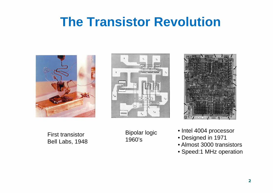
The Transistor Revolution
First transistorBell Labs, 1948
Bipolar logic1960’s
• Intel 4004 processor • Designed in 1971• Almost 3000 transistors• Speed:1 MHz operation

Transistors
• Can be classified as:– BJT – Bipolar Junction Transistor;
• Bipolar device (two carriers)
• Current controlled device
– FET – Field Effect Transistor;
• Unipolar device (single carrier)
• Voltage controlled device
3
4
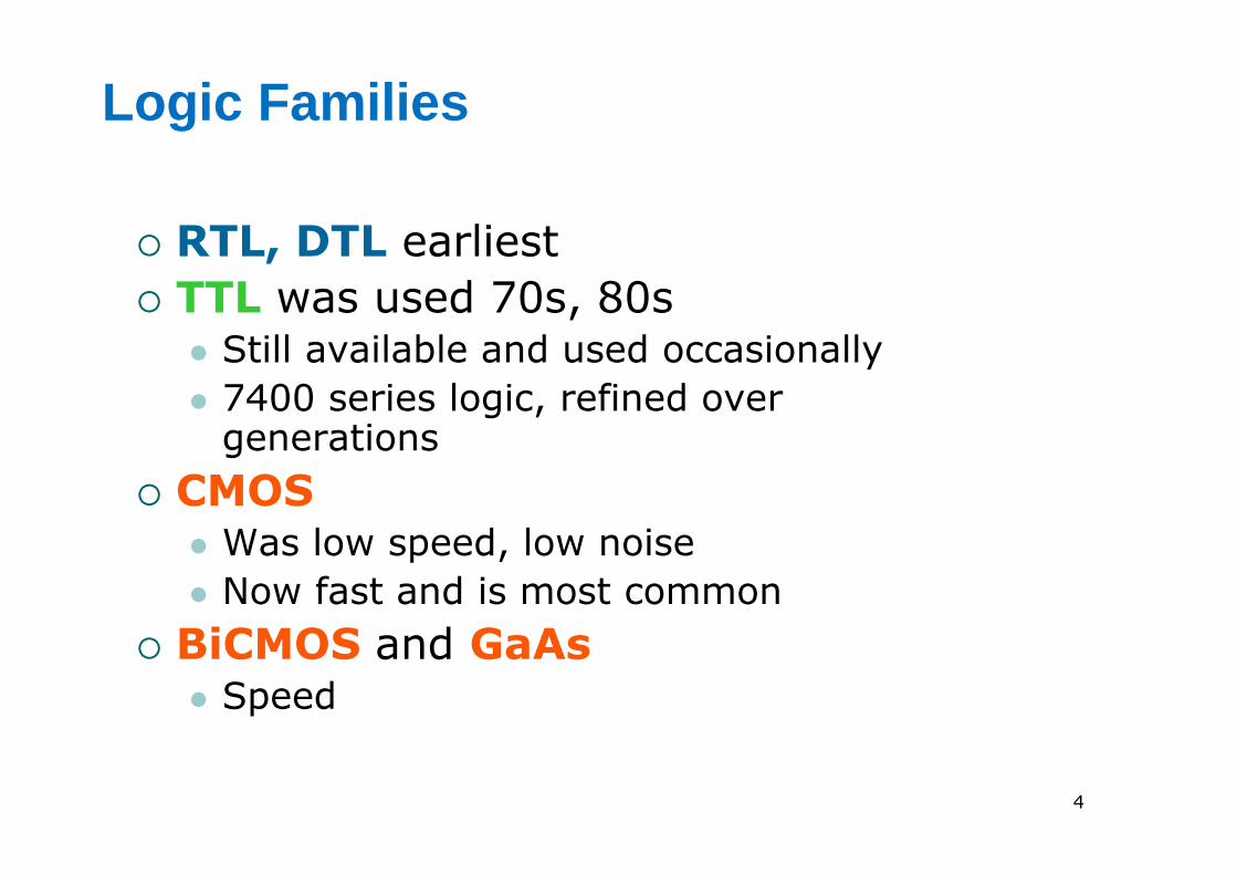
Logic Families
� RTL, DTL earliest
� TTL was used 70s, 80s� Still available and used occasionally
� 7400 series logic, refined over generations
� CMOS� Was low speed, low noise
� Now fast and is most common
� BiCMOS and GaAs� Speed

CMOS Technology

Semiconductor Materialso Electronic materials generally can be divided
into three categories:• Insulators• Semiconductors• Conductors
o The primary parameter used to distinguish among these materials is the resistivity(rho)
• Insulator 105 < rho• Semiconductors 10-3 < rho < 105
• Conductors rho < 10-3
o Silicon and germanium are the most important semiconductor materials
6

P-type and N -typeo The real advantage of semiconductors
emerge when impurities are added to the material in minute amounts (Doping)
o Impurity doping enables us to change the resistivity over a very wide range and determine whether the electron or holepopulation controls the resistivity of the material.
� Donor Impurities: have five valence electrons in the outer shell (phosphorus and arsenic). Semiconductors doped with donor impurities are called n-type.
� Acceptor Impurities: have one less electron than silicon in the outer shell (boron). Semiconductors doped with acceptor impurities are known as p-type.
7

8
MOSFET: MetalOxideSemiconductor
Field Effect Transistor
A voltage controlled device�Dissipates less power �Achieves higher density on an IC� Has full swing voltage 0 � 5V

9
The MOS Transistor
Polysilicon
Aluminum
10
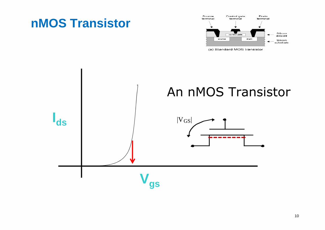
nMOS Transistor
Ids
Vgs
|VGS|
An nMOS Transistor

11
Transistor as a Switch
VGS ≥ VT
RonS D
A Switch!
|VGS|
An MOS Transistor
12
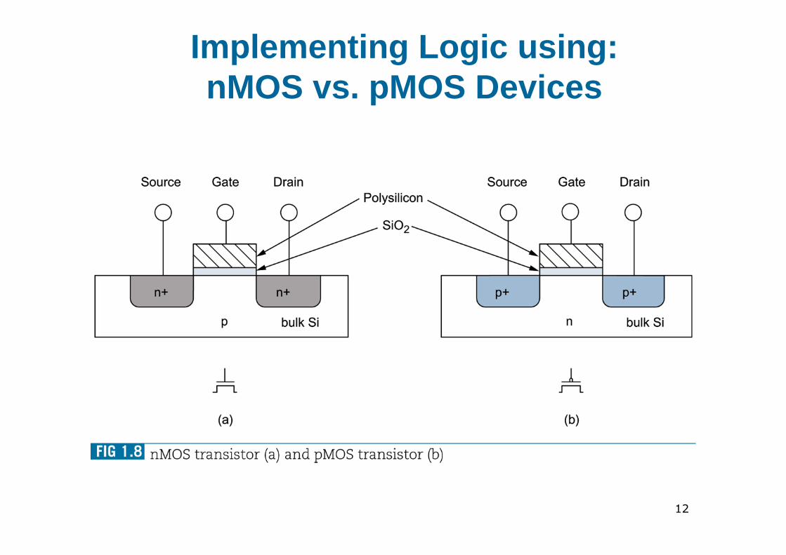
Implementing Logic using: nMOS vs. pMOS Devices

13
Complementary MOS (CMOS)
VDD
F(In1,In2,…InN)
In1In2
InN
In1In2
InN
PUN
PDN
PMOS only
NMOS only
PUN and PDN are dual logic networks
At every point in time (except during the switching transients) each gate output is connected to either VDD or VSS via a low resistive path
VSS
ON
OFF
OFF
ON
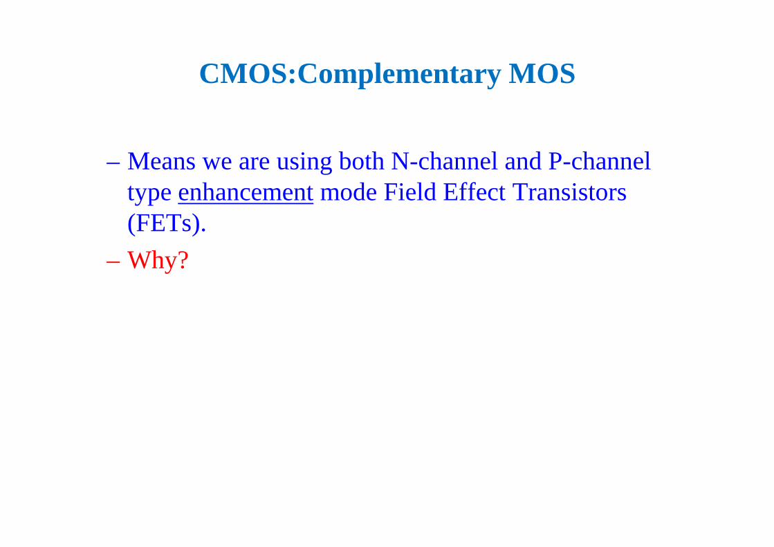
CMOS:Complementary MOS
– Means we are using both N-channel and P-channel type enhancement mode Field Effect Transistors (FETs).
– Why?

15
Threshold Drops
VDD
0 → VDD
CL
PUN
0 → VDD - VTn
CL
VDD
VDD
S
D S
D
VGS
VDD → 0PDN
CLVDD
VDD → |VTp|
CL
S
SD
D
VGS
Weak ‘1’
Weak ‘0’
Strong ‘1’
Strong ‘0’
Use PMOS Transistors in Pull Up Network
Use NMOS Transistors in Pull down Network

16
Complementary MOS (CMOS)
o NMOS Transistors pass a ``strong” 0 but a ``weak” 1
o PMOS Transistors pass a ``strong” 1 but a ``weak” 0
o Combining both would lead to circuits that can pass strong 0’s and strong 1’s
X Y
C
C

17
CMOS Inverter
A Y
0
1
VDD
A Y
GNDA Y
Pull-up Network
Pull-down Network

18
CMOS Inverter
A Y
0
1 0
VDD
A=1 Y=0
GND
ON
OFF
A Y

19
CMOS Inverter
A Y
0 1
1 0
VDD
A=0 Y=1
GND
OFF
ON
A Y

20
CMOS Tri-State Inverter
A Y
E A Y
0 X Z
1 0 1
1 1 0
E
E
A
Y

21
NMOS Transistors
in Series/Parallel Connection
Transistors can be thought as a switch controlled by its gate signal
NMOS switch closes when switch control input is high
X Y
A B
Y = X if A and B
X Y
A
B Y = X if A OR B
NMOS Transistors pass a “strong” 0 but a “weak” 1
In Series
In Parallel
22
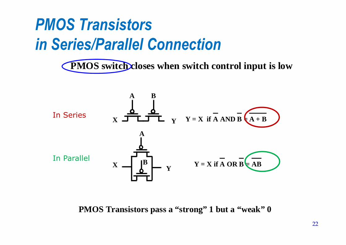
PMOS Transistors
in Series/Parallel Connection
X Y
A B
Y = X if A AND B = A + B
X Y
A
B Y = X if A OR B = AB
PMOS Transistors pass a “strong” 1 but a “weak” 0
PMOS switch closes when switch control input is low
In Series
In Parallel

23
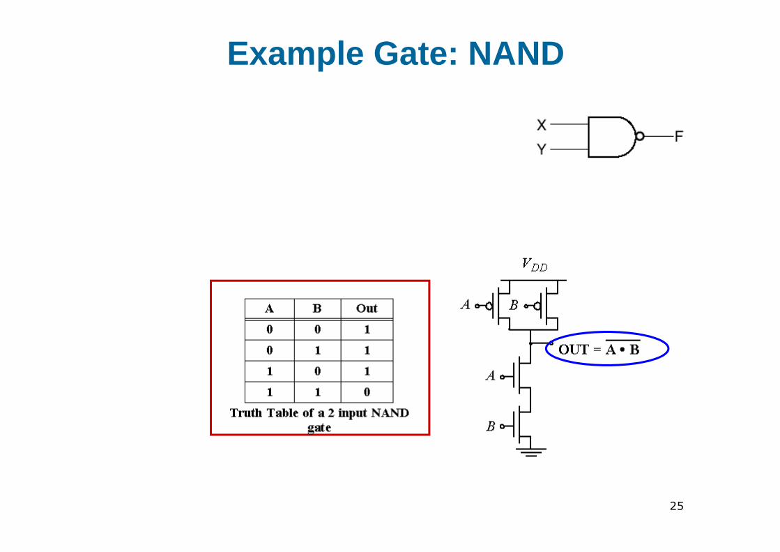
Example Gate: NAND
X Y
A B
Y = X if A an d B
X Y
A
B Y = X if A O R B
N M O S T ransisto rs pass a “strong ” 0 b u t a “w eak” 1
Pull Down Network

24
Example Gate: NAND
X Y
A B
Y = X if A AND B = A + B
X Y
A
B Y = X if A OR B = AB
PMOS Transistors pass a “strong” 1 but a “weak” 0
PMOS switch closes when switch control input is low
Pull Up Network
25
Example Gate: NAND
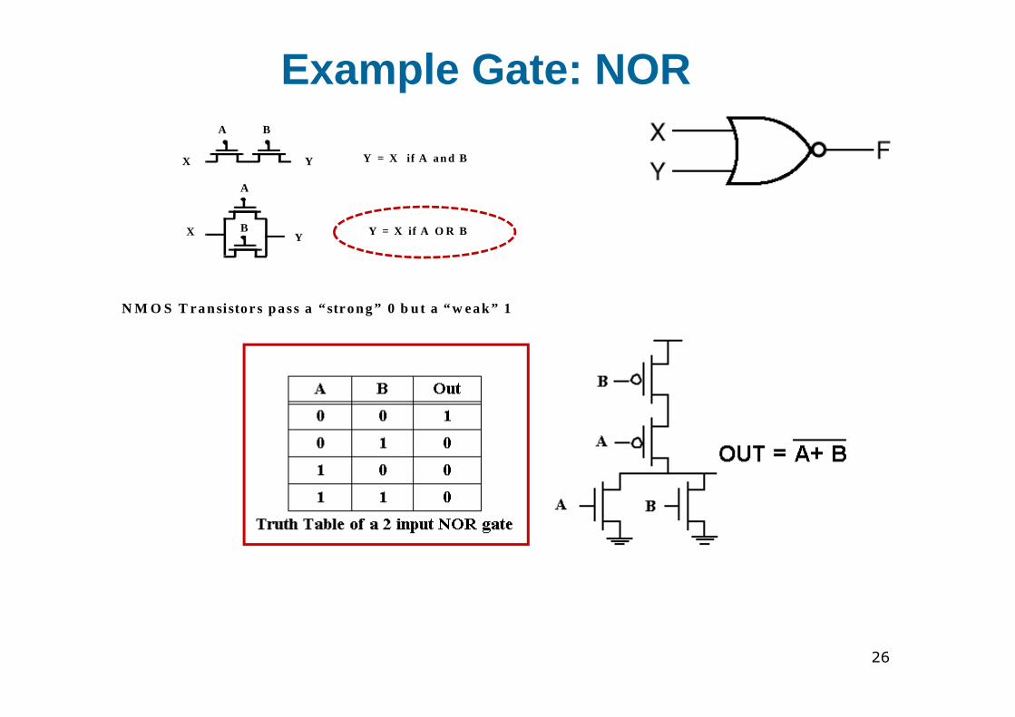
Example Gate: NOR
26
X Y
A B
Y = X if A an d B
X Y
A
B Y = X if A O R B
N M O S T ransisto rs pass a “strong ” 0 b u t a “w eak” 1

27
Construction of Compound Gates
․ Example: ․ Step 1 (n-network): Invert F to derive n-network
․ Step 2 (n-network): Make connections of transistors: AND ⇔ Series connection (A.B) …. (C.D) OR ⇔ Parallel connection ((A.B) + (C.D))

28
Construction of Compound Gates
․ Example: ․ Step 1 (n-network): Invert F to derive n-network
․ Step 2 (n-network): Make connections of transistors: AND ⇔ Series connection (A.B) series, (C.D) also in series OR ⇔ Parallel connection ((A.B) + (C.D)) in parallel

29
Construction of Compound Gates (cont’d)
․ Step 3 (p-network): Expand F to derive p-network
each input is inverted
․ Step 4 (p-network): Make connections of transistors (same as Step 2).

30
Construction of Compound Gates (cont’d)
․ Step 3 (p-network): Expand F to derive p-network
each input is inverted
․ Step 4 (p-network): Make connections of transistors (same as Step 2).
․ Step 5: Connect the n-network to GND (typically, 0V) and the p-network to VDD (5V, 3.3V, or 2.5V, etc).

31
Complex CMOS Gate
OUT = D + A • (B + C)
D
A
B C
D
A
B
C
32
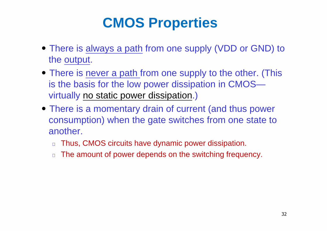
CMOS Properties
․There is always a path from one supply (VDD or GND) to the output.․There is never a path from one supply to the other. (This
is the basis for the low power dissipation in CMOS—virtually no static power dissipation.)․There is a momentary drain of current (and thus power
consumption) when the gate switches from one state to another.
Thus, CMOS circuits have dynamic power dissipation. The amount of power depends on the switching frequency.
