eng2410 the von neumann computer digital design...
TRANSCRIPT

School of Engineering 1
ENG2410Digital Design
“Programmable Logic Technologies”
Fall 2017S. Areibi
School of EngineeringUniversity of Guelph
2
Week #12 Topics
� The Von Neumann Architecture
� What is Programmable Logic?
� Classification of Programmable Logic
� Field Programmable Gate Arrays
� FPGA CAD
� Applications
� Summary
3
Resources
� Chapter #10, Mano Sections� 10.3 Programmable Implementations Tech
4
� Principle
In 1945, the mathematician Von Neumann (VN)
demonstrated in study of computation that a
computer could have a simple structure,
capable of executing any kind of program,
given a properly programmed control unit,
without the need of hardware modification
The Von Neumann Computer
ENIAC - The first electronic computer (1946)
5
� Structure
� An arithmetic and logic unit (ALU) also called data path for program execution
� A control unit (control path) featuring a program counter for controlling program execution
� A memory for storing program and data.
� The memory consists of the word with the same length
Datapath
Control Unit
Processor orCentral processing unit
Dataand
Instructions
Addressregister
Memory
Instructionregister PC
Data
Address
Registers
The Von Neumann Computer
6
The Von Neumann Computer
� Coding
A program is coded as a set of instructions to be
sequentially executed
� Program execution
� Instruction Fetch (IF): The next instruction to be executed is fetched from the memory
� Decode (D): Instruction is decoded (operation?)
� Read operand (R): Operands read from the memory
� Execute (EX): Operation is executed on the ALU
� Write result (W): Results written back to the memory
� Instruction execution in Cycle (IF, D, R, EX, W)
What is the problem with this computing paradigm?
School of Engineering 2
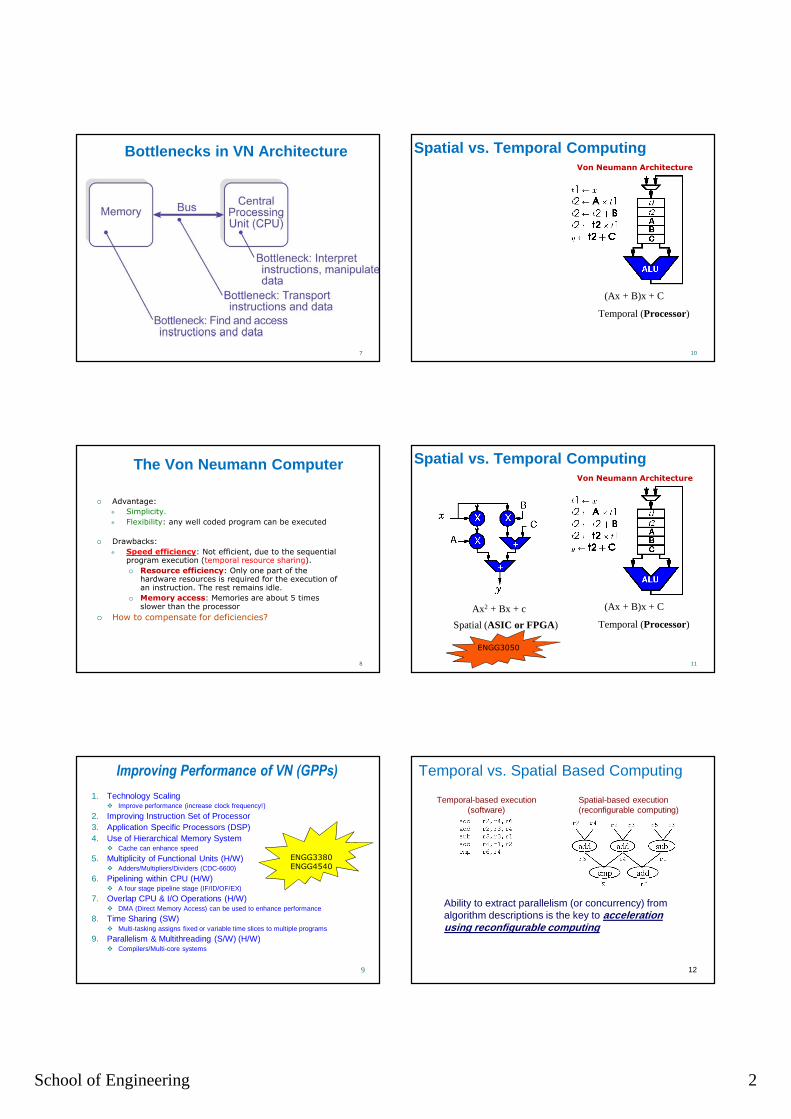
Bottlenecks in VN Architecture
7
8
The Von Neumann Computer
� Advantage:
� Simplicity.
� Flexibility: any well coded program can be executed
� Drawbacks:
� Speed efficiency: Not efficient, due to the sequential program execution (temporal resource sharing).
� Resource efficiency: Only one part of the hardware resources is required for the execution of an instruction. The rest remains idle.
� Memory access: Memories are about 5 times slower than the processor
� How to compensate for deficiencies?
9
Improving Performance of VN (GPPs)
1. Technology Scaling� Improve performance (increase clock frequency!)
2. Improving Instruction Set of Processor3. Application Specific Processors (DSP)4. Use of Hierarchical Memory System
� Cache can enhance speed
5. Multiplicity of Functional Units (H/W)� Adders/Multipliers/Dividers (CDC-6600)
6. Pipelining within CPU (H/W)� A four stage pipeline stage (IF/ID/OF/EX)
7. Overlap CPU & I/O Operations (H/W) � DMA (Direct Memory Access) can be used to enhance performance
8. Time Sharing (SW)� Multi-tasking assigns fixed or variable time slices to multiple programs
9. Parallelism & Multithreading (S/W) (H/W)� Compilers/Multi-core systems
ENGG3380ENGG4540
10
Spatial vs. Temporal Computing
(Ax + B)x + C
Temporal (Processor)
Von Neumann Architecture
11
Spatial vs. Temporal Computing
Ax2 + Bx + c (Ax + B)x + C
Spatial (ASIC or FPGA) Temporal (Processor)
ENGG3050
Von Neumann Architecture
Temporal vs. Spatial Based Computing
Temporal-based execution(software)
Spatial-based execution(reconfigurable computing)
Ability to extract parallelism (or concurrency) from algorithm descriptions is the key to acceleration using reconfigurable computing
12

School of Engineering 3
Estrin at work.
Substantial effortson Reconfiguration
Gerald Estrin Fix-Plus Machine
� Attempts to have a flexible hardware structure that can be dynamically modified at run-time to compute a desired function are almost as old as the development of other computing paradigms.
� In 1959, Gerald Estrin, at UCLA, introduced the concept of reconfigurable computing by introducing the Fix-Plus Machine.
14
Programmable Logic I
ProgrammableOr Array
ProgrammableAND array
� We learnt in the first part of this course that any combinational logic circuit can be implemented with the sum of min-terms (SOP).
� If we can control the number of AND gates to be used and also control the inputs to the OR gate then we can design a programmable logic circuit.
� Remember when we used a decoder to implement any Boolean function! That was some type of implementing programmable logic!
15
I. Programmable AND Array
o If we remove fuses Faf and Fbt this will disconnect the complementary
version of input ‘a’ and the true version of input ‘b’.
o This leaves the device to perform its new function � y = a AND b’
o The process of removing fuses is typically referred to as programming
the device (blowing, burning the device).
o Devices based on fusible-link technology are said to be One Time
Programmable (OTP).
o Remember: FPGAs are not based on this type of technology.
16
Decoders: Implementing Logic
� Example: Implement the following boolean functions 1. S(A2,A1,A0) = SUM(m(1,2,4,7))
1. Since there are three inputs, we need a 3-to-8 line decoder.
2. The decoder generates the eight minterms for inputs A0,A1,A2
3. An OR GATE forms the logical sum minterms required.
17
II. Programmable OR Array
Programmable Boolean Functions
Multiplexers can also be used to realize Boolean functions since they consist of an array of AND gates followed by an OR gate.
18

School of Engineering 4
19
Classification of PLDs
ProgrammableOr Array
ProgrammableAND array
ProgrammableOr Array
ProgrammableAND array
20
Classification
The first programmable
ICs were generically
referred to as (PLDs).
Programmable Logic Devices
Simple PLDs Complex PLDs
21
Programmable Logic Array (PLA)
Like programmable
inverterTied to 0 – F1
not invertedTied to 1 – F1 is
inverted
1
2
34
The integration of several Simple PLD blocks with a programmable interconnect on a single chip � CPLD
PLDBlock
PLDBlock
Interconnection MatrixI/O
Block
I/O B
lock
PLDBlock
PLDBlock
I/O B
lock
I/O B
lock
•••
Interconnection Matrix
•••
•••
•••
Complex PLDs (CPLDs)
22
23
III. SRAM FPGAs:
Memory units can be used to implement a Boolean function by storing the output of the truth table in the memory and accessing the values by using variables of the truth table as address lines.
A B C D Z
0 0 0 0 0 0 0 0 1 1 0 0 1 0 1 0 0 1 1 1 0 1 0 0 0 0 1 0 1 1 0 1 1 0 1 0 1 1 1 1 1 0 0 0 0 1 0 0 1 1 1 0 1 0 1 1 0 1 1 1 1 1 0 0 0 1 1 0 1 0 1 1 1 0 0
A B C D Z
0 0 0 0 0 0 0 0 1 1 0 0 1 0 1 0 0 1 1 1 0 1 0 0 0 0 1 0 1 1 0 1 1 0 1 0 1 1 1 1 1 0 0 0 0 1 0 0 1 1 1 0 1 0 1 1 0 1 1 1 1 1 0 0 0 1 1 0 1 0 1 1 1 0 0
LUT
ABCD
Z
LUT implementation
AB
CD
Z
Gate implementation
24
Generic FPGA architecture:Configurable Logic Block (CLB) � LUT + FF
Connection Block
Switch Block
Routing Channels
I/O pad
Wire segments

School of Engineering 5
25
SRAM based Programmable Cell
o There are two main versions of semiconductor RAM devices:o Dynamic RAM (DRAM) and
o Static RAM (SRAM).
o SRAM based devices can be used to control NMOS transistors to be on/off.
o This can be very useful to control Multiplexers, Routing, e.t.c.
26
Pass Transistor
o An SRAM cell can drive the gate (G) terminal of an NMOS transistor.
o If SRAM (M) = 1 then signals passes from S � D
o An SRAM cell can be attached to the select line of a MUX to control it.
27
Look Up Table (LUT)
o The LUT is used to realize any boolean function.
o Assume the function to be realized is y = (a&b) | !c
o This could be achieved by loading the LUT with the appropriate output values
28
Configurable Logic Block (CLB)
A Configurable logic block consists of lookup table (LUT), a register that could act as flip flop or a latch, and a mulitplexer, along with a few other elements.
29
Xili
nx C
LB
30
Switch Matrix
o Connections between CLBs and IOBs are made using wiring segments in both horizontal and vertical channels lying between the various blocks.
o Four segments meet, on each there is 6 pass transistors.

School of Engineering 6
31
Xilinx IOB
32
Design Entry
Logic Optimization
Synthesis
Mapping to k-LUT
Packing LUTs to CLBs
Placement
Routing Configure an FPGA
Simulation
CAD for FPGAs
33
CAD for FPGAs: Place & Route
Design Entry
Logic Optimization
Synthesis
Mapping to k-LUT
Packing LUTs to CLBs
Placement
Routing Configure an FPGA
Simulation
34
f2
f3
f1
Programming an FPGA?
A
B
C
DEF
f1
f2 f3
ABC
DEF
Technology Mapping
Placement
Routing
35
FPGA Placement Problem• Input – A technology mapped netlist of Configurable
Logic Blocks ( CLB ) realizing a given circuit.
• Output – CLB netlist placed in a two dimensional array of slots such that total wirelength is minimized.
CLB Netlist
i1 i2 i3 i4
f1 f2
1 2 3
4 5 6 7 8
9 10
FPGA
Placement
i1 i2 i3
i4
f2
f1
1
2
3
4
56
7
8
9
10
36
Global vs. Detailed Routing
� Global routing
LB LB LB
SB SB
LB LB LB
SB SB
LB LB LB
SB
SB
LB LB LB
SB SB
LB LB LB
SB SB
LB LB LB
SB
SB
� Detailed routing

School of Engineering 7
37
Remember!
Program
mable
Lookup Tables (LUTs)
Program
mable
routing structure
Main bottleneck with state-of-the-art fine grain FPGAs is the routing enabled by pass transistors!
38
Remember!
Program
mable
Lookup Tables (LUTs)
Program
mable
routing structure
LUTxyz f
...
fSRAM
x
y
z...
001
0
...
1
Look-up-tables are flexible but require lots of configuration and suffer from power dissipation!
39
Fine Grain FPGAs: Spartan2
o 4K bit RAM blocks
o Large amount of logic
o Program stored in SRAM
40
Medium Grain: Xilinx Virtex• Virtex-II FPGA introduced followed by Virtex-II Pro in 2003
– 444 18x18 Multipliers & 18kbit block RAMs introduced– Gbit Serial I/O Communications & Power PC Processors Introduced– Complex Floating Point Algorithm Implementation now possible
• Virtex-II / Pro– 44,000 Logic Slices– 444 18Kbits BRAMs– 444 18x18 Multipliers– 2 PowerPC
Processors– 20 Gbit I/O– 1164 Max User I/O
Zynq - Extensible Processing Platform
41
Configuration Port or ICAP
Configuration Port
Dynamic Partial Reconfiguration� Partial Reconfiguration is the ability to dynamically modify blocks of logic
while the remaining logic continues to operate without interruption.� Computation sequences are not know at compile time . The system decides,
respectively reacts dynamically to application driven reconfiguration requests.
Full
Bit File
Partial
Bit Files
Fu
nctio
n A
1
Fu
nctio
n B
1
Fu
nctio
n C
1F
un
ction
C2
Fu
nctio
n B
2
Fu
nctio
n A
2F
un
ction
A3
42

School of Engineering 8
Methods for executing algorithms
Advantages:•very high performance and efficient
Disadvantages:•not flexible (can’t be altered after fabrication)
• expensive
Hardware(Application Specific Integrated Circuits)
Software-programmedprocessors
Advantages:•software is very flexible to change
Disadvantages:•performance can suffer if clock is not fast
•fixed instruction set by hardware
Reconfigurablecomputing
Advantages:•fills the gap between hardware and software
•much higher performance than software
•higher level of flexibility than hardware 43
44
Reconfigurable Devices
Reconfigurable Devices (RD) are usually used in many different ways:
1. Rapid Prototyping
2. Non-frequent reconfigurable systems
3. Frequently reconfigurable systems
4. High Performance Computing (Acceleration of Complex Algorithms
45
1. Rapid prototyping
� Testing hardware in real conditions before fabrication
� Software simulation
� Relatively inexpensive
� Slow
� Accuracy ?
� Hardware emulation
� Hardware testing under real operation conditions
� Fast
� Accurate
� Allow several iterations
APTIX System Explorer
ITALTEL FLEXBENCH
46
2. Non-Frequent Reconfiguration
47
3. Frequently Reconfigured
Computing systems that are able to adapt their behaviourand structure to changing operating and environmental conditions, time-varying optimization objectives, and physical constraints like changing protocols, new standards, or dynamically changing operation conditions of technical systems
48
4. Algorithm Acceleration
Real Time Video Processing - Single Precision Floating
Point calculations
-36 GFlops + 40 GOPs
sustained Performance on
a single PCI card
- >200 times Power
reduction over Xeon
Gravity Simulation - N-Body computation
- Single Precision FloatingPoint
- 20GFlops/sec sustainedperformance
-100 times faster than2.4GHz Pentium 4 CPU
School of Engineering 9
49
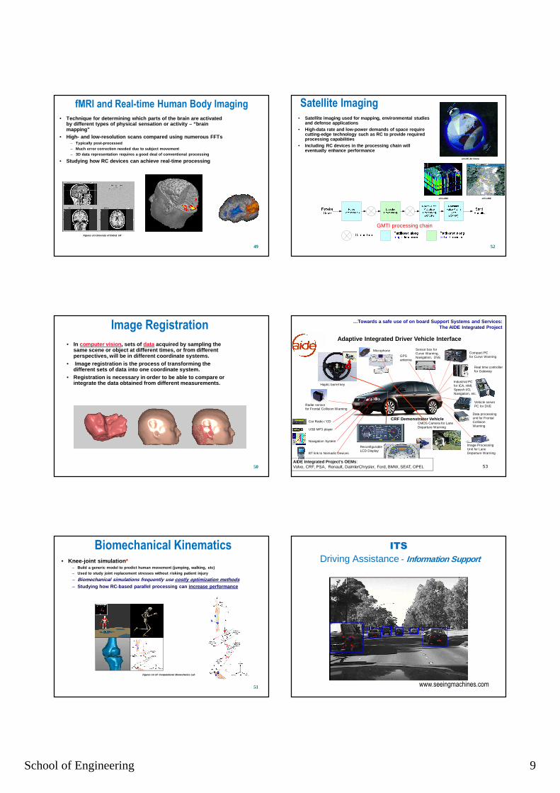
fMRI and Real-time Human Body Imaging
• Technique for determining which parts of the brain are activated by different types of physical sensation or activit y – “brain mapping”
• High- and low-resolution scans compared using numero us FFTs– Typically post-processed– Much error correction needed due to subject movemen t– 3D data representation requires a good deal of conv entional processing
• Studying how RC devices can achieve real-time proce ssing
Figures c/o University of Oxford, UK
50
Image Registration
• In computer vision , sets of data acquired by sampling the same scene or object at different times, or from di fferent perspectives, will be in different coordinate syste ms.
• Image registration is the process of transforming t he different sets of data into one coordinate system.
• Registration is necessary in order to be able to co mpare or integrate the data obtained from different measurem ents.
51
Biomechanical Kinematics • Knee-joint simulation *
– Build a generic model to predict human movement (ju mping, walking, etc)– Used to study joint replacement stresses without ri sking patient injury
– Biomechanical simulations frequently use costly opt imization methods– Studying how RC-based parallel processing can incre ase performance
Figures c/o UF Computational Biomechanics Lab
52
Satellite Imaging• Satellite imaging used for mapping, environmental s tudies
and defense applications• High-data rate and low-power demands of space requi re
cutting-edge technology such as RC to provide requi red processing capabilities
• Including RC devices in the processing chain will eventually enhance performance
GMTI processing chain
c/o LANLc/o LANL
c/o US Air Force
Adaptive Integrated Driver Vehicle Interface
…Towards a safe use of on board Support Systems and Services: The AIDE Integrated Project
AIDE Integrated Project’s OEMs : Volvo, CRF, PSA, Renault, DaimlerChrysler, Ford, BMW, SEAT, OPEL
CRF Demonstrator Vehicle
Reconfigurable LCD Display
Microphone
Radar sensorfor Frontal Collision Warning
Compact PCfor Curve Warning
Data processing unit for Frontal Collision Warning
GPS antenna
Vehicle server PC for DVE
Image Processing Unit for Lane Departure Warning
Industrial PC for ICA, HMI, Speech I/O, Navigation, etc.
Car Radio / CD
USB MP3 player
Navigation System
BT link to Nomadic Devices
Real time controller for Gateway
CMOS Camera for Lane Departure Warning
Sensor box for Curve Warning,Navigation, DVE
Haptic barrel key
53
ITS
Driving Assistance - Information Support
www.seeingmachines.com

School of Engineering 10
55
Summaryo Programmable logic comes in different flavors such as PLDs,
CPLDs and FPGAs.
o Field Programmable Gate Arrays is a technology introduced in the late 80’s to allow Engineers to implement their design without the need to fabricate the chip as we do in Application Specific Integrated Circuits (ASICs).
o The main components of an FPGA are the CLBs, IOBs and programmable interconnect (Fine Grain FPGAs).
o New technologies of FPGAs include Block Memory, Processors, Multipliers (we start to call these Coarse Grain FPGAs)
o Applications of FPGAs in HPC, Embedded Systems, Cars, Appliances, … (Endless ..)
57
Programming
• Programming the PLA can be specified in tabular form
• 3 sections,
1. product terms,
2. input and AND gates,
3. Outputs