features functional block diagram adc dgnd · functional block diagram dgnd dvdd agnd avdd ref1 vin...
TRANSCRIPT

FUNCTIONAL BLOCK DIAGRAM
AVDDDVDD REF1AGNDDGND
VIN (+)
VIN (–)
P/S
REF2
XTALCLKIN
UNI
DB15DB14
CAL
RESETSYNC
CS
DVAL/RD
CFMT/DRDY
DB3/TSI
DB4/DOE
DB5/SFMT
DB6/FSI
DB7/SCO
DB8/SDO
16-BIT A/D CONVERTER
-MODULATOR
FIRFILTER
CLOCKCIRCUITRY
CONTROLLOGIC
DB13
AD7722 2.5VREFERENCE
DB12DB11DB10DB9/FSO
DB0DB1DB2
FEATURES
16-Bit - ADC
64 Oversampling Ratio
Up to 220 kSPS Output Word Rate
Low-Pass, Linear Phase Digital Filter
Inherently Monotonic
On-Chip 2.5 V Voltage Reference
Single-Supply 5 V
High Speed Parallel or Serial Interface
GENERAL DESCRIPTIONThe AD7722 is a complete low power, 16-bit, Σ-∆ ADC. Thepart operates from a 5 V supply and accepts a differential inputvoltage range of 0 V to +2.5 V or ±1.25 V centered around acommon-mode bias. The AD7722 provides 16-bit performancefor input bandwidths up to 90.625 kHz. The part provides dataat an output word rate of 195.3 kHz.
The analog input is continuously sampled by an analog modula-tor, eliminating the need for external sample-and-hold circuitry.The modulator output is processed by two finite impulse response(FIR) digital filters in series. The on-chip filtering reduces theexternal antialias requirements to first order, in most cases. Thegroup delay for the filter is 215.5 µs, while the settling time fora step input is 431 µs. The sample rate, filter corner frequency,and output word rate are set by an external clock that isnominally 12.5 MHz.
Use of a single bit DAC in the modulator guarantees excellentlinearity and dc accuracy. Endpoint accuracy is ensured on-chipby calibration. This calibration procedure minimizes the zero-scale and full-scale errors.
Conversion data is provided at the output register through a flex-ible serial port or a parallel port. This offers 3-wire, high speedinterfacing to digital signal processors. The serial interface operatesin an internal clocking (master) mode, whereby an internal serialdata clock and framing pulse are device outputs. Additionally,two AD7722s can be configured with the serial data outputsconnected together. Each converter alternately transmits its conver-sion data on a shared serial data line.
The part provides an accurate on-chip 2.5 V reference. Areference input/output function is provided to allow either theinternal reference or an external system reference to be used asthe reference source for the part.
The AD7722 is available in a 44-lead MQFP package and isspecified over the industrial temperature range of –40°C to +85°C.

REV. C–2–
AD7722–SPECIFICATIONS1(AVDD = AVDD1 = 5 V 5%; DVDD = 5 V 5%; AGND = AGND1 = DGND = 0 V;
UNI = Logic Low or High; fCLKIN = 12.5 MHz; fS = 195.3 kSPS; REF2 = 2.5 V; TA = TMIN to TMAX, unless otherwise noted.)
A VersionParameter Test Conditions/Comments Min Typ Max Unit
DYNAMIC SPECIFICATIONS2
Bipolar Mode, UNI = VINH VCM = 2.5 V, VIN(+) = VIN(–) =1.25 V p-p,or VIN(–) = 1.25 V, VIN(+) = 0 V to 2.5 V
Signal-to-(Noise + Distortion)3 Input Bandwidth 0 kHz–90.625 kHz 86/84.5 90 dBInput Bandwidth 0 kHz–100 kHz, fCLKIN = 14 MHz 84.5/83 dB
Total Harmonic Distortion3 Input Bandwidth 0 kHz–90.625 kHz –90/–88 dBInput Bandwidth 0 kHz–100 kHz, fCLKIN = 14 MHz –88/–86 dB
Spurious-Free Dynamic Range Input Bandwidth 0 kHz–90.625 kHz –90 dBInput Bandwidth 0 kHz–100 kHz, fCLKIN = 14 MHz –88 dB
Unipolar Mode, UNI = VINL VIN(–) = 0 V, VIN(+) = 0 V to 2.5 VSignal-to-(Noise + Distortion)3 Input Bandwidth 0 kHz–90.625 kHz 84.5/83 88 dBTotal Harmonic Distortion3 Input Bandwidth 0 kHz–97.65 kHz –89/–87 dBSpurious-Free Dynamic Range Input Bandwidth 0 kHz–97.65 kHz –90 dB
Intermodulation Distortion –93 dBAC CMRR VIN(+) = VIN(–) = 2.5 V p-p
VCM = 1.25 V to 3.75 V, 20 kHz 96 dBDigital Filter Response
Pass-Band Ripple 0 kHz to 90.625 kHz ±0.005 dBCutoff Frequency 96.92 kHzStop-Band Attenuation 104.6875 kHz to 12.395 MHz 90 dB
ANALOG INPUTSFull-Scale Input Span VIN(+) – VIN(–)
Bipolar Mode UNI = VINH –VREF2/2 +VREF2/2 VUnipolar Mode UNI = VINL 0 VREF2 V
Absolute Input Voltage VIN(+) and VIN(–) 0 AVDD VInput Sampling Capacitance 2 pFInput Sampling Rate Guaranteed by Design 2 × fCLKIN HzDifferential Input Impedance 1/(4 × 10-9)fCLKIN kΩ
CLOCKCLKIN Mark Space Ratio 45 55 %
REFERENCEREF1 Output Voltage 2.32 2.47 2.62 VREF1 Output Voltage Drift 60 ppm/°CREF1 Output Impedance 3 kΩReference Buffer
Offset Voltage Offset between REF1 and REF2 ±12 mVUsing Internal Reference
REF2 Output Voltage 2.32 2.47 2.62 VREF2 Output Voltage Drift 60 ppm/°C
Using External ReferenceREF2 Input Impedance REF1 = AGND 1/(16 × 10−9)fCLKIN kΩExternal Reference Voltage Range Applied to REF1 or REF2 2.32 2.5 2.62 V
STATIC PERFORMANCEResolution 16 BitsDifferential Nonlinearity Guaranteed Monotonic ±0.5 ±1 LSBIntegral Nonlinearity ±2 LSBAfter Calibration
Offset Error4 ±3 mVGain Error4, 5 ±0.6 % FSR
Without CalibrationOffset Error ±6 mVGain Error5 ±0.6 % FSR
Offset Error Drift ±1 LSB/°CGain Error Drift REF2 Is an Ideal Reference, REF1 = AGND
Unipolar Mode ±1 LSB/°CBipolar Mode ±0.5 LSB/°C

REV. C
AD7722
–3–
A VersionParameter Test Conditions/Comments Min Typ Max Unit
LOGIC INPUTS (Excluding CLKIN)VINH, Input High Voltage 2.0 VVINL, Input Low Voltage 0.8 V
CLOCK INPUT (CLKIN)VINH, Input High Voltage 4.0 VVINL, Input Low Voltage 0.4 V
ALL LOGIC INPUTSIIN, Input Current VIN = 0 V to DVDD ±10 µACIN, Input Capacitance 10 pF
LOGIC OUTPUTSVOH, Output High Voltage |IOUT| = 200 µA 4.0 VVOL, Output Low Voltage |IOUT| = 1.6 mA 0.4 V
POWER SUPPLIESAVDD, AVDD1 4.75 5.25 VDVDD 4.75 5.25 VIDD Total from AVDD and DVDD 75 mAPower Consumption 375 mW
NOTES1Operating temperature range is –40°C to +85°C (A Version).2Measurement Bandwidth = 0.5 × fS; Input Level = –0.05 dB.3TA = 25°C to 85°C/TA = TMIN to TMAX.4Applies after calibration at temperature of interest.5Gain error excludes reference error. The ADC gain is calibrated w.r.t. the voltage on the REF2 pin.
Specifications subject to change without notice.

REV. C–4–
AD7722ABSOLUTE MAXIMUM RATINGS1
(TA = 25°C, unless otherwise noted.)
DVDD to DGND . . . . . . . . . . . . . . . . . . . . . . . .–0.3 V to +7 VAVDD, AVDD1 to AGND . . . . . . . . . . . . . . . . . .–0.3 V to +7 VAVDD, AVDD1 to DVDD . . . . . . . . . . . . . . . . . . . –1 V to +1 VAGND, AGND1 to DGND . . . . . . . . . . . . . –0.3 V to +0.3 VDigital Inputs to DGND . . . . . . . . . . –0.3 V to DVDD + 0.3 VDigital Outputs to DGND . . . . . . . . . –0.3 V to DVDD + 0.3 VVIN(+), VIN(–) to AGND . . . . . . . . . . –0.3 V to AVDD + 0.3 VREF1 to AGND . . . . . . . . . . . . . . . . –0.3 V to AVDD + 0.3 VREF2 to AGND . . . . . . . . . . . . . . . . –0.3 V to AVDD + 0.3 VDGND, AGND1, AGND2 . . . . . . . . . . . . . . . . . . . . . . ±0.3 VInput current to any pin except the supplies2 . . . . . . . . ±10 mAOperating Temperature Range . . . . . . . . . . . –40°C to +85°CStorage Temperature Range . . . . . . . . . . . . –65°C to +150°CJunction Temperature . . . . . . . . . . . . . . . . . . . . . . . . . . 150°CθJA Thermal Impedance . . . . . . . . . . . . . . . . . . . . . . . . 72°C/WθJC Thermal Impedance . . . . . . . . . . . . . . . . . . . . . . . . 20°C/WLead Temperature, Soldering
Vapor Phase (60 sec) . . . . . . . . . . . . . . . . . . . . . . . . . 215°CInfrared (15 sec) . . . . . . . . . . . . . . . . . . . . . . . . . . . . 220°C
NOTES1Stresses above those listed under Absolute Maximum Ratings may causepermanent damage to the device. This is a stress rating only; functional opera -tion of the device at these or any other conditions above those indicated in theoperational section of this specification is not implied. Exposure to absolutemaximum rating conditions for extended periods may affect device reliability.
2Transient currents up to 100 mA will not cause SCR latch-up.
IOL1.6mA
IOH200A
1.6VCL
50pF
TOOUTPUT
PIN
Figure 1. Load Circuit for Timing Specifications

REV. C
AD7722
–5–
TIMING SPECIFICATIONSParameter Symbol Min Typ Max Unit
CLKIN Frequency fCLK 0.3 12.5 15 MHzCLKIN Period (tCLK = 1/fCLK) t1 0.067 0.08 3.33 µsCLKIN Low Pulse Width t2 0.45 × t1 0.55 × t1
CLKIN High Pulse Width t3 0.45 × t1 0.55 × t1
CLKIN Rise Time t4 5 nsCLKIN Fall Time t5 5 nsFSI Low Time t6 2 tCLK
FSI Setup Time t7 20 nsFSI Hold Time t8 20 nsCLKIN to SCO Delay t9 40 nsSCO Period1 t10 2 tCLK
SCO Transition to FSO High Delay t11 4 10 nsSCO Transition to FSO Low Delay t12 4 10 nsSCO Transition to SDO Valid Delay t13 3 8 nsSCO Transition from FSI2 t14 2.5 tCLK
SDO Enable Delay Time t15 30 45 nsSDO Disable Delay Time t16 10 30 ns
DRDY High Time t17 2 tCLK
Conversion Time1 t18 64 tCLK
DRDY to CS Setup Time t19 0 nsCS to RD Setup Time t20 0 nsRD Pulse Width t21 tCLK + 20 nsData Access Time after RD Falling Edge3 t22 tCLK + 40 nsBus Relinquish Time after RD Rising Edge t23 tCLK + 40 nsCS to RD Hold Time t24 0 nsRD to DRDY High Time t25 1 tCLK
SYNC/RESET Input Pulse Width t26 10 nsDVAL Low Delay from SYNC/RESET t27 40 nsSYNC/RESET Low Time after CLKIN Rising t28 10 tCLK – 10 nsDRDY High Delay after SYNC/RESET Low t29 50 nsDRDY Low Delay after SYNC/RESET Low1 t30 (8192 + 64) tCLK
DVAL High Delay after SYNC/RESET Low1 t31 8192 tCLK
CAL Setup Time t34 10 nsCAL Pulse Width t35 1 2 tCLK
Calibration Delay from CAL High t36 64 tCLK
Unipolar Input Calibration Time, (UNI = 0)1, 4 t37 (3 × 8192 + 2 × 512) tCLK
Bipolar Input Calibration Time, (UNI = 1)1, 4 t37 (4 × 8192 + 3 × 512) tCLK
Conversion Results Valid, (UNI = 0)1 t38 (3 × 8192 + 2 × 512 + 64) tCLK
Conversion Results Valid, (UNI = 1)1 t38 (4 × 8192 + 3 × 512 + 64) tCLK
NOTES1Guaranteed by design.2Frame sync is initiated on falling edge of CLKIN.3With RD synchronous to CLKIN, t22 can be reduced up to 1 tCLK.4See Figure 8.
Specifications subject to change without notice.
(AVDD = 5 V 5%, DVDD = 5 V 5%, AGND = DGND = 0 V, CL = 50 pF, TA = TMIN to TMAX, fCLKIN = 12.5 MHz, SFMT = Logic Low or High, CFMT = Logic Low or High.)

REV. C–6–
AD7722
ZERO FOR LAST 16 SCO CYCLESVALID DATA FOR 16 SCO CYCLES VALID
CLKIN
SCO(CFMT = 0)
FSO(SFMT = 0)
SCO
32 SCO CYCLES
64 CKLIN CYCLES
Figure 2a. Generalized Serial Mode Timing (FSI = Logic Low or High, TSI = DOE)
ZERO FOR LAST 16 SCO CYCLESVALID DATA FOR 16 SCO CYCLES VALID
CLKIN
SCO(CFMT = 0)
FSO(SFMT = 1)
SCO
HIGH FOR LAST 16 SCO CYCLESLOW FOR 16 SCO CYCLES
64 CKLIN CYCLES
32 SCO CYCLES
Figure 2b. Generalized Serial Mode Timing (FSI = Logic Low or High, TSI = DOE)
t2
t3
t4 t5
0.8V2.3V
t8 t1 t6
t7 t9
t9 t10
CLKIN
FSI
SCO
Figure 3. Serial Mode Timing for Clock Input, Frame Sync Input, and Serial Clock Output
CLKIN
LOW FORD15–D0
t1
t10
t11 t12
t14
t13
t13
D15 D14 D13 D1 D0
D15 D14 D13 D1 D0
t12 t11
FSI
SCO
FSO
SDO
SCO
FSO
SDO
SFMT = LOGICLOW(0)
SFMT = LOGICHIGH(1)
Figure 4. Serial Mode Timing for Frame Sync Input, Frame Sync Output, Serial Clock Output,and Serial Data Output (CFMT = Logic Low, TSI = DOE)

REV. C
AD7722
–7–
t15 t16
DOE
SDO
Figure 5. Serial Mode Timing for Data Output Enable and Serial Data Output (TSI = Logic Low)
t17
t20
t21
t23
RD
DB0–DB15
t22
VALID DATA
t25
t24
t18
t19
CS
DRDY
Figure 6. Parallel Mode Read Timing
CLKIN
t29
t30
t31
t27
t26
t28 MAXt28 MIN
SYNC, RESET
DVAL
DRDY
Figure 7. SYNC and RESET Timing, Serial and Parallel Mode
CLKIN
SYNC, RESET
DVAL
DRDY
8192 tCLK 8192 tCLK 8192 tCLK 8192 tCLK
512 tCLK512 tCLK512 tCLK
t38
t34
t37 UNI = 1
t37 UNI = 0
t35
t36
Figure 8. Calibration Timing, Serial and Parallel Mode

REV. C–8–
AD7722PIN FUNCTION DESCRIPTIONS
Mnemonic Pin No. Description
AVDD1 14 Clock Logic Power Supply Voltage for the Analog Modulator, 5 V ± 5%.
AGND1 10 Clock Logic Ground Reference for the Analog Modulator.
AVDD 20, 23 Analog Power Supply Voltage, 5 V ± 5%.
AGND 9, 13, 15, 19, Ground Reference for Analog Circuitry.21, 25, 26
DVDD 39 Digital Power Supply Voltage, 5 V ± 5%.
DGND 6, 28 Ground Reference for Digital Circuitry.
REF1 22 Reference Input/Output. REF1 connects through 3 kΩ to the output of the internal 2.5 V reference andto the input of a buffer amplifier that drives the Σ-∆ modulator. This pin can also be overdriven with anexternal reference 2.5 V.
REF2 24 Reference Input/Output. REF2 connects to the output of an internal buffer amplifier used to drive theΣ-∆ modulator. When REF2 is used as an input, REF1 must be connected to AGND.
VIN(+) 18 Positive Terminal of the Differential Analog Input.
VIN(–) 16 Negative Terminal of the Differential Analog Input.
UNI 7 Analog Input Range Select Input. UNI selects the analog input range for either bipolar or unipolaroperation. A logic low input selects unipolar operation. A logic high input selects bipolar operation.
CLKIN 11 Clock Input. Master clock signal for the device. The CLKIN pin interfaces the AD7722 internaloscillator circuit to an external crystal or an external clock. A parallel resonant, fundamental-frequency,microprocessor-grade crystal and a 1 MΩ resistor should be connected between the CLKIN andXTAL pins with two capacitors connected from each pin to ground. Alternatively, the CLKIN pincan be driven with an external CMOS compatible clock. The AD7722 is specified with a clock inputfrequency of 12.5 MHz.
XTAL 12 Oscillator Output. The XTAL pin connects the internal oscillator output to an external crystal.If an external clock is used, XTAL should be left unconnected.
P/S 8 Parallel/Serial Interface Select Input. A logic high configures the output data interface for parallel modeoperation. The serial mode operation is selected with the P/S set to a logic low.
CAL 27 Calibration Logic Input. A logic high input for a duration of one CLKIN cycle initiates acalibration sequence for the device gain and offset error.
RESET 17 Reset Logic Input. RESET is used to clear the offset and gain calibration registers. RESET is anasynchronous input. RESET allows the user to set the AD7722 to an uncalibrated state if thedevice had been previously calibrated. A rising edge also resets the AD7722 Σ-∆ modulator byshorting the integrator capacitors in the modulator. In addition, RESET functions identically tothe SYNC pin described below. When operating with more than one AD7722, a RESET/SYNCshould be issued following power up to ensure the devices are synchronized. Ensure that thesupplies are settled before applying the RESET/SYNC pulse.
CS 29 Chip select is a level sensitive logic input. CS enables the output data register for parallel mode readoperation. The CS logic level is sensed on the rising edge of CLKIN. The output data bus is enabledwhen the rising edge of CLKIN senses a logic low level on CS if RD is also low. When CS is sensedhigh, the output data bits DB15–DB0 will be high impedance. In serial mode, tie CS to a logic low.
SYNC 30 Synchronization Logic Input. SYNC is an asynchronous input. When using more than oneAD7722 operated from a common master clock, SYNC allows each ADC’s Σ-∆ modulator tosimultaneously sample its analog input and update its output data register. A rising edge resetsthe AD7722 digital filter sequencer counter to zero. After a SYNC, conversion data is not valid untilafter the digital filter settles (see Figure 7). DVAL goes low in the serial mode. When the risingedge of CLKIN senses a logic low on SYNC (or RESET), the reset state is released; in parallelmode, DRDY goes high. After the reset state is released, DVAL returns high after 8192 CLKINcycles (128 × 64/fCLKIN); in parallel mode, DRDY returns low after one additional convolution cycleof the digital filter (64 CLKIN periods), when valid data is ready to be read from the output dataregister. When operating with more than one AD7722, a RESET/SYNC should be issued follow-ing power up to ensure the devices are synchronized. Ensure that the supplies are settled beforeapplying the RESET/SYNC pulse.

REV. C
AD7722
–9–
PIN CONFIGURATION 44-Lead MQFP (S-44-2)
3
4
5
6
7
1
2
10
11
8
9
40 39 3841424344 36 35 3437
29
30
31
32
33
27
28
25
26
23
24
PIN 1IDENTIFIER
TOP VIEW(Not to Scale)
12 13 14 15 16 17 18 19 20 21 22
AD7722
DGND/DB13
DGND/DB14
DGND/DB15
SYNC
CS
DGND
CAL
AGND
AGND
REF2
AVDD
DGND/DB2
DGND/DB1
DGND/DB0
CFMT/DRDY
DVAL/RD
DGND
UNI
P/S
AGND
AGND1
CLKIN
TS
I/DB
3
DO
E/D
B4
SF
MT
/DB
5
FS
I/DB
6
SC
O/D
B7
DV
DD
SD
O/D
B8
FS
O/D
B9
DG
ND
/DB
10
DG
ND
/DB
11
DG
ND
/DB
12
XT
AL
AG
ND
AV
DD
1
AG
ND
VIN
(–)
RE
SE
T
VIN
(+)
AG
ND
AV
DD
AG
ND
RE
F1
PARALLEL MODE PIN FUNCTION DESCRIPTIONS
Mnemonic Pin No. Description
DVAL/RD 5 Read input is a level sensitive logic input. The RD logic level is sensed on the rising edge of CLKIN. Thisdigital input can be used in conjunction with CS to read data from the device. The output data bus isenabled when the rising edge of CLKIN senses a logic low level on RD if CS is also low. When RD issensed high, the output data bits DB15–DB0 will be high impedance.
CFMT/DRDY 4 Data Ready Logic Output. A falling edge indicates a new output word is available to be read from theoutput data register. DRDY will return high upon completion of a read operation. If a read operation doesnot occur between output updates, DRDY will pulse high for two CLKIN cycles before the next outputupdate. DRDY also indicates when conversion results are available after a SYNC or RESET sequenceand when completing a self-calibration.
DGND/DB15 31 Data Output Bit (MSB).DGND/DB14 32 Data Output Bit.DGND/DB13 33 Data Output Bit.DGND/DB12 34 Data Output Bit.DGND/DB11 35 Data Output Bit.DGND/DB10 36 Data Output Bit.FSO/DB9 37 Data Output Bit.SDO/DB8 38 Data Output Bit.SCO/DB7 40 Data Output Bit.FSI/DB6 41 Data Output Bit.SFMT/DB5 42 Data Output Bit.DOE/DB4 43 Data Output Bit.TSI/DB3 44 Data Output Bit.DGND/DB2 1 Data Output Bit.DGND/DB1 2 Data Output Bit.DGND/DB0 3 Data Output Bit (LSB).

REV. C–10–
AD7722SERIAL MODE PIN FUNCTION DESCRIPTIONS
Mnemonic Pin No. Description
DVAL/RD 5 Data Valid Logic Output. A logic high on DVAL indicates that the conversion result in the outputdata register is an accurate digital representation of the analog voltage at the input to the - modu-lator. The DVAL pin is set low for 8,192 CLKIN cycles if the analog input is overranged and afterinitiating CAL, SYNC, or RESET.
CFMT/DRDY 4 Serial Clock Format Logic Input. The clock format pin selects whether the serial data, SDO, is validon the rising or falling edge of the serial clock, SCO. When CFMT is logic low, SDO is valid on thefalling edge of SCO if SFMT is low; SDO is valid on the rising edge of SCO if SFMT is high. WhenCFMT is logic high, SDO is valid on the rising edge of SCO if SFMT is low; SDO is valid on thefalling edge of SCO if SFMT is high.
TSI/DB3 44 Time Slot Logic Input. The logic level on TSI sets the active state of the DOE pin. With TSI setlogic high, DOE will enable the SDO output buffer when it is a logic high, and vice versa. TSI is usedwhen two AD7722s are connected to the same serial data bus. When using a single ADC, connectTSI to DGND.
DOE/DB4 43 Data Output Enable Logic Input. The DOE pin controls the three-state output buffer of the SDOpin. The active state of DOE is determined by the logic level on the TSI pin. When the DOE logiclevel equals the level on the TSI pin, the serial data output, SDO, is active. Otherwise, SDO will behigh impedance. SDO can be three-state after a serial data transmission by connecting DOE to FSO.This input is useful when two AD7722s are connected to the same serial data bus. When using asingle ADC, to ensure SDO is active, connect DOE to DGND so that it equals the logic level of TSI.
SFMT/DB5 42 Serial Data Format Logic Input. The logic level on the SFMT pin selects the format of the FSOsignal. A logic low makes the FSO output a pulse one SCO cycle wide occurring every 32 SCO cycles.With SFMT set to a logic high, the FSO signal is a frame pulse that is active low for the duration ofthe 16 data bit transmission.
FSI/DB6 41 Frame Synchronization Logic Input. The FSI input is used to synchronize the AD7722 serial outputdata register to an external source. When the falling edge of CLKIN detects a low-to-high transition,the AD7722 interrupts the current data transmission, reloads the output serial shift register, resetsSCO, and transmits the conversion result. Synchronization starts immediately, and the next 127conversions are invalid. In serial mode, DVAL remains high. FSI inputs applied synchronous to theoutput data rate do not alter the serial data transmission. If FSI is tied to either a logic high or low,the AD7722 will generate FSO outputs controlled by the logic level on SFMT.
SCO/DB7 40 Serial Data Clock Output. The serial clock output is synchronous to the CLKIN signal and has afrequency one-half the CLKIN frequency. A data transmission frame is 32 SCO cycles long.
SDO/DB8 38 Serial Data Output. The serial data is shifted out MSB first, synchronous with the SCO. A serialdata transmission lasts 32 SCO cycles. After the LSB is output, trailing zeros are output for theremaining 16 SCO cycles.
FSO/DB9 37 Frame Sync Output. This output indicates the beginning of a word transmission on the SDO pin.Depending on the logic level of the SFMT pin, the FSO signal is either a positive pulse approximatelyone SCO period wide or a frame pulse, which is active low for the duration of the 16 data bit trans-mission (see Figure 4).
DGND/DB0 3 In serial mode, these pins should be tied to DGND.
DGND/DB1 2
DGND/DB2 1
DGND/DB10 36
DGND/DB11 35
DGND/DB12 34
DGND/DB13 33
DGND/DB14 32
DGND/DB15 31
REV. C
AD7722
–11–
TERMINOLOGYSignal-to-Noise Plus Distortion Ratio (S/(N+D))S/(N+D) is the measured signal-to-noise plus distortion ratioat the output of the ADC. The signal is the rms magnitude ofthe fundamental. Noise plus distortion is the rms sum of allnonfundamental signals and harmonics to half the sampling rate(fCLKIN/128), excluding dc. The ADC is evaluated by applying alow noise, low distortion sine wave signal to the input pins. Bygenerating a fast Fourier transform (FFT) plot, the S/(N+D) datacan then be obtained from the output spectrum.
Total Harmonic Distortion (THD)THD is the ratio of the rms sum of the harmonics to the rmsvalue of the fundamental. THD is defined as
THD = 20 logSQRT V2
2 +V 32 +V 4
2 +V52 +V6
2( )V1
where V1 is the rms amplitude of the fundamental, and V2, V3,V4, V5, and V6 are the rms amplitudes of the second throughsixth harmonics. The THD is also derived from the FFT plot ofthe ADC output spectrum.
Spurious-Free Dynamic Range (SFDR)Defined as the difference in dB between the peak spurious or har-monic component in the ADC output spectrum (up to fCLKIN/128and excluding dc) and the rms value of the fundamental. Normally,the value of this specification will be determined by the largestharmonic in the output spectrum of the FFT. For input signalswhose second harmonics occur in the stop-band region of thedigital filter, a spur in the noise floor limits the SFDR.
Intermodulation DistortionWith inputs consisting of sine waves at two frequencies, fa andfb, any active device with nonlinearities will create distortionproducts at sum and difference frequencies of mfa ± nfb, wherem, n = 0, 1, 2, 3, and so on. Intermodulation distortion terms arethose for which neither m nor n is equal to zero. For example, thesecond order terms include (fa + fb) and (fa – fb), while the thirdorder terms include (2fa + fb), (2fa – fb), (fa + 2fb) and (fa – 2fb).
Testing is performed using the CCIF standard, where two inputfrequencies near the top end of the input bandwidth are used.In this case, the second order terms are usually distanced infrequency from the original sine waves, while the third orderterms are usually at a frequency close to the input frequencies.As a result, the second and third order terms are specifiedseparately. The calculation of the intermodulation distortion isas per the THD specification, where it is the ratio of the rmssum of the individual distortion products to the rms amplitudeof the sum of the fundamental, expressed in dB.
Pass-Band RippleThe frequency response variation of the AD7722 in the definedpass-band frequency range.
Pass-Band FrequencyThe frequency up to which the frequency response variation iswithin the pass-band ripple specification.
Cutoff FrequencyThe frequency below which the AD7722’s frequency responsewill not have more than 3 dB of attenuation.
Stop-Band FrequencyThe frequency above which the AD7722’s frequency responsewill be within its stop-band attenuation.
Stop-Band AttenuationThe AD7722’s frequency response will not have less than 90 dBof attenuation in the stated frequency band.
Integral NonlinearityThis is the maximum deviation of any code from a straight linepassing through the endpoints of the transfer function. Theendpoints of the transfer function are minus full scale, a point0.5 LSB below the first code transition (100 . . . 00 to 100 . . .01 in bipolar mode, 000 . . . 00 to 000 . . . 01 in unipolar mode)and plus full scale, a point 0.5 LSB above the last code transition(011 . . . 10 to 011 . . . 11 in bipolar mode, 111 . . . 10 to111 . . . 11 in unipolar mode). The error is expressed in LSB.
Differential NonlinearityThis is the difference between the measured and the ideal 1 LSBchange between two adjacent codes in the ADC.
Common-Mode Rejection RatioThe ability of a device to reject the effect of a voltage applied toboth input terminals simultaneously—often through variation ofa ground level—is specified as a common-mode rejection ratio.CMRR is the ratio of gain for the differential signal to the gainfor the common-mode signal.
Unipolar Offset ErrorUnipolar offset error is the deviation of the first code transition(00 . . . 000 to 00 . . . 001) from the ideal differential voltage(VIN(+) – VIN(–) + 0.5 LSB) when operating in the unipolar mode.
Bipolar Offset ErrorThis is the deviation of the midscale transition code(111 . . . 11 to 000 . . . 00) from the ideal differential voltage(VIN(+) – VIN(–) – 0.5 LSB) when operating in the bipolar mode.
Gain ErrorThe first code transition should occur at an analog value 1/2 LSBabove – full scale. The last transition should occur for an analogvalue 1 1/2 LSB below the nominal full scale. Gain error is thedeviation of the actual difference between first and last codetransitions and the ideal difference between first and last codetransitions.

REV. C–12–
AD7722–Typical Performance Characteristics(AVDD = DVDD = 5.0 V, TA = 25C; CLKIN = 12.5 MHz, AIN = 20 kHz, Bipolar Mode; VIN(+) = 0 V to 2.5 V, VIN(–) = 1.25 V, unless otherwise noted.)
INPUT LEVEL (dB)
dB
110
100
50–40 –30 0–20 –10
90
80
70
60
SFDR
S/ (N+D)
TPC 1. S/(N+D) and SFDR vs.Analog Input Level
INPUT FREQUENCY (kHz)
–85
–90
–1150 20 10040 60 80
–95
–100
–105
–110
THD
SNR
SFDR
VIN (+) = V IN(–) = 1.25V p-pVCM = 2.5V
dB
TPC 4. SNR, THD, and SFDRvs. Input Frequency
TEMPERATURE (C)
–94
–116–50 –25 1000 25 50 75
–96
–108
–110
–112
–114
–100
–102
–106
–104
–98 THD
3RD
4TH
2ND
dB
TPC 7. THD vs. Temperature
OUTPUT DATA RATE (kSPS)
84
92
85
88
89
90
91
86
87
0 50 300100 150 200 250
AIN = 1/5 BW
dB
TPC 2. S/(N+D) vs. OutputSample Rate
OUTPUT DATA RATE (kSPS)
84
92
85
88
89
90
91
86
87
0 50 300100 150 200 250
AIN = 1/5 BWVIN (+) = V IN (–) = 1.25V p-pVCM = 2.5V
dB
TPC 5. S/(N+D) vs. OutputSample Rate
CODES
FR
EQ
UE
NC
Y O
F O
CC
UR
RE
NC
E
5000
0n–3 n–2 n+3n–1 n n+1 n+2
4500
2000
1500
1000
500
4000
3500
2500
3000
VIN(+) = V IN(–) CLKIN = 12.5MHz 8k SAMPLES
TPC 8. Histogram of OutputCodes with DC Input
INPUT FREQUENCY (kHz)
dB
–85
–90
–1150 20 10040 60 80
–95
–100
–105
–110
SNR
SFDR
THD
TPC 3. SNR, THD, and SFDRvs. Input Frequency
TEMPERATURE (C)
92.0
91.5
88.0–50 0 10050
90.0
89.5
88.5
89.0
91.0
90.5
dB
TPC 6. SNR vs. Temperature
CODE
DN
L E
RR
OR
(L
SB
)
1.0
0.8
–1.00 20000 6553540000
–0.4
–0.8
–0.6
0
–0.2
0.6
0.2
0.4
TPC 9. Differential Nonlinearity

REV. C
AD7722
–13–
CODE
INL
ER
RO
R (
LS
B)
1.0
0.8
–1.00 20000 6553540000
–0.4
–0.8
–0.6
0
–0.2
0.6
0.2
0.4
TPC 10. Integral Nonlinearity Error
0
–154
dB
–20
–80
–100
–120
–140
–40
–60
0 10 20 30 40 50 60 70 80 98
CLKIN = 12.5MHz SNR = 90.1dB S/(N+D) = 89.2dB SFDR = –99.5dB THD = –96.6dB 2ND = –100.9dB 3RD = –106.0dB 4TH = –99.5dB
FREQUENCY (kHz)
TPC 11. 16K Point FFT
0
–154
dB
–20
–80
–100
–120
–140
–40
–60
0 20 40 60 80 96
XTAL = 12.288MHz SNR = 89.0dB S/(N+D) = 87.8dB SFDR = –94.3dB THD = –93.8dB 2ND = –94.3dB 3RD = –108.5dB 4TH = –105.7dB
FREQUENCY (kHz)
TPC 12. 16K Point FFT
CLKIN FREQUENCY (MHz)
PO
WE
R (
mW
)
200
00 2.5 15.010.0 12.5
180
80
60
40
20
160
140
100
120
5.0 7.5
AIDD
DIDD
TPC 13. Power Consumption vs. CLKIN Frequency
0
–154
dB
–20
–80
–100
–120
–140
–40
–60
0 20 40 60 80 96
AIN = 90kHz XTAL = 12.288MHz SNR = 88.1dB S/(N+D) = 88.1dB SFDR = –103.7dB
FREQUENCY (kHz)
TPC 14. 16K Point FFT
0
–154
dB
–20
–80
–100
–120
–140
–40
–60
0 20 40 60 80 98
AIN = 90kHz CLKIN = 12.5 MHz SNR = 89.6dB S/(N+D) = 89.6dB SFDR = –108.0dB
FREQUENCY (kHz)
TPC 15. 16K Point FFT

REV. C–14–
AD7722CIRCUIT DESCRIPTIONThe AD7722 ADC employs a Σ-∆ conversion technique thatconverts the analog input into a digital pulse train. The analoginput is continuously sampled by a switched capacitor modulatorat twice the rate of the clock input frequency, 2 × fCLKIN. Thedigital data that represents the analog input is in the ones densityof the bit stream at the output of the Σ-∆ modulator. The modu-lator outputs a bit stream at a data rate equal to fCLKIN.
Due to the high oversampling rate, which spreads the quantizationnoise from 0 to fCLKIN/2, the noise energy contained in the bandof interest is reduced (Figure 9a). To reduce the quantizationnoise further, a high order modulator is employed to shape thenoise spectrum so that most of the noise energy is shifted out ofthe band of interest (Figure 9b).
The digital filter that follows the modulator provides three mainfunctions. The filter performs sophisticated averaging on the1-bit samples from the output of the modulator, while removingthe large out of band quantization noise (Figure 9c). Lastly, thedigital filter reduces the data rate from fCLKIN at the input of thefilter to fCLKIN/64 at the output of the filter. The AD7722 outputdata rate, fS, is a little over twice the signal bandwidth, whichguarantees that there is no loss of data in the signal band.
Digital filtering has certain advantages over analog filtering. First,since digital filtering occurs after the A/D conversion, it canremove noise injected during the conversion process. Analogfiltering cannot remove noise injected during conversion. Second,the digital filter combines low pass-band ripple with a steep roll-offwhile also maintaining a linear phase response.
BAND OF INTERESTfCLKIN /2
DIGITAL FILTER CUTOFF FREQUENCYWHICH EQUALS 97.65kHz (12.5MHz)
BAND OF INTEREST
QUANTIZATION NOISE
fCLKIN /2
BAND OF INTERESTfCLKIN /2
NOISE SHAPING
a.
b.
c.
Figure 9. Σ-∆ ADC
The AD7722 employs two finite impulse response (FIR) filters inseries. The first filter is a 384-tap filter that samples the output ofthe modulator at fCLKIN. The second filter is a 151-tap half-bandfilter that samples the output of the first filter at fCLKIN/32 anddecimates by 2. The implementation of this filter architectureresults in a filter with a group delay of 42 conversions (84 conver-sions for settling to a full-scale step).
The digital filter provides 6 dB of attenuation at a frequency(fCLKIN/128) one-half its output rate. With a clock frequencyof 12.5 MHz, the digital filter has a pass-band frequency of90.625 kHz, a cutoff frequency is 96.92 kHz, and a stop-bandfrequency of 104.6875 kHz.
Due to the sampling nature of the digital filter, the filter does notprovide any rejection at integer multiples of its input samplingfrequency. The filter response in Figure 10a shows the unattenu-ated frequency bands occurring at n × fCLKIN where n = 1, 2, 3. . . .At these frequencies, there are frequency bands ± f3 dB wide(f3 dB is the –3 dB bandwidth of the digital filter) on either sideof n × fCLKIN where noise passes unattenuated to the output.Out-of-band signals coincident with any of the filter images arealiased into the pass band. However, due to the AD7722’s highoversampling ratio, these bands occupy only a small fraction ofthe spectrum, and most broadband noise is filtered. This meansthat the antialias filtering requirements in front of the AD7722are considerably reduced versus a conventional converter with noon-chip filtering. Figure 10b shows the frequency response of anantialias filter. With a –3 dB corner frequency set at fCLKIN/64,a single-pole filter will provide 36 dB of attenuation at fCLKIN.
Depending on the application, however, it may be necessary toprovide additional antialias filtering prior to the AD7722 toeliminate unwanted signals from the frequency bands the digitalfilter passes. It may also be necessary in some applications toprovide analog filtering in front of the AD7722 to ensure thatdifferential noise signals outside the band of interest do notsaturate the analog modulator.
1fCLKIN
0dB
2fCLKIN 3fCLKIN
Figure 10a. Digital Filter Frequency Response
OUTPUTDATA RATE
fCLKIN/ 64
0dB
fCLKIN
ANTIALIAS FILTERRESPONSE
REQUIREDATTENUATION
Figure 10b. Frequency Response of Antialias Filter
REV. C
AD7722
–15–
APPLYING THE AD7722Analog Input RangeThe AD7722 uses differential inputs to provide common-modenoise rejection (i.e., the converted result will correspond to thedifferential voltage between the two inputs). The absolute voltageon both inputs must lie between AGND and AVDD.
In unipolar mode, the full-scale analog input range(VIN(+) – VIN(–)) is 0 V to VREF2. The output code is straightbinary in the unipolar mode with 1 LSB = 38 µV. The ideal transferfunction is shown in Figure 11.
In bipolar mode, the full-scale input range is ±VREF2/2. Thebipolar mode allows complementary input signals. As anotherexample, in bipolar mode, VIN(–) can be connected to a dc biasvoltage to allow a single-ended input on VIN(+) equal to VBIAS
±VREF2/2. In bipolar mode, the output code is twos complementwith 1 LSB = 38 µV. The ideal transfer function is shown inFigure 12.
111...111
111...110
111...101
111...100
000...011
000...010
000...001
000...000
OUTPUTCODE
0V VREF2 –1LSBDIFFERENTIAL INPUT VOLTAGE VIN(+) – V IN(–)
Figure 11. Unipolar Mode Transfer Function
111...111
111...110
100...001
100...000
000...010
000...001
000...000
OUTPUTCODE
0V
+VREF2/ 2 – 1LSB
DIFFERENTIAL INPUT VOLTAGE VIN(+) – V IN(–)
–VREF2
011...111
011...110
Figure 12. Bipolar Mode Transfer Function
Differential InputsThe analog input to the modulator is a switched capacitor design.The analog signal is converted into charge by highly linearsampling capacitors. A simplified equivalent circuit diagram ofthe analog input is shown in Figure 13. A signal source drivingthe analog input must be able to provide the charge onto thesampling capacitors every half CLKIN cycle and settle to therequired accuracy within the next half cycle.
18
ΦA
ΦB
ΦA
ΦB16
2pF
2pF
ACGROUND
500
ΦA ΦB ΦA ΦBCLKIN
VIN(+)
VIN(–)
AD7722500
Figure 13. Analog Input Equivalent Circuit
Since the AD7722 samples the differential voltage across itsanalog inputs, low noise performance is attained with an inputcircuit that provides low common-mode noise at each input.The amplifiers used to drive the analog inputs play a critical rolein attaining the high performance available from the AD7722.
When a capacitive load is switched onto the output of an op amp,the amplitude will momentarily drop. The op amp will try tocorrect the situation and, in the process, will hit its slew rate limit.This nonlinear response, which can cause excessive ringing, canlead to distortion. To remedy the situation, a low-pass RC filtercan be connected between the amplifier and the input to theAD7722 as shown in Figure 14. The external capacitor at eachinput aids in supplying the current spikes created during thesampling process. The resistor in this diagram, as well as creatingthe pole for the antialiasing, isolates the op amp from the transientnature of the load.
ANALOGINPUT
R
CAD7722
VIN(+)
VIN(–)R
C
Figure 14. Simple RC Antialiasing Circuit
The differential input impedance of the AD7722 switched capacitorinput varies as a function of the CLKIN frequency, given by theequation
Zf
kINCLKIN
=×
104
9
Ω

REV. C–16–
AD7722Even though the voltage on the input sampling capacitors may nothave enough time to settle to the accuracy indicated by the resolu-tion of the AD7722, as long as the sampling capacitor chargingfollows the exponential curve of RC circuits, only the gainaccuracy suffers if the input capacitor is switched away too early.
An alternative circuit configuration for driving the differentialinputs to the AD7722 is shown in Figure 15.
R100
C2.7nF
AD7722
VIN(+)
VIN(–)
C2.7nF
C2.7nF
R100
Figure 15. Differential Input with Antialiasing
A capacitor between the two input pins sources or sinks chargeto allow most of the charge that is needed by one input to beeffectively supplied by the other input. This minimizes undesir-able charge transfer from the analog inputs to and from ground.The series resistor isolates the operational amplifier from thecurrent spikes created during the sampling process and providesa pole for antialiasing. The –3 dB cutoff frequency (f3 dB) of theantialias filter is given by Equation 1, and the attenuation of thefilter is given by Equation 2.
fRCdB3
16
=
(1)
Attenuation logf
f dB= +
20 1 / 13
2
(2)
The choice of the filter cutoff frequency will depend on theamount of roll-off that is acceptable in the pass band of thedigital filter and the required attenuation at the first imagefrequency. For example, when operating the AD7722 with a12.5 MHz clock, with the typical values of R and C of 100 Ω and2.7 nF shown in Figure 15, the –3 dB cutoff frequency (f3 dB)creates less than 1 dB of in-band (90.625 kHz) roll-off andprovides about 36 dB attenuation at the first image frequency.
The capacitors used for the input antialiasing circuit must havelow dielectric absorption to avoid distortion. Film capacitors suchas polypropylene, polystyrene, or polycarbonate are suitable. Ifceramic capacitors are used, they must have NP0 dielectric.
Applying the ReferenceThe reference circuitry used in the AD7722 includes an on-chip2.5 V band gap reference and a reference buffer circuit. The blockdiagram of the reference circuit is shown in Figure 16. The inter-nal reference voltage is connected to REF1 through a 3 kΩ resistorand is internally buffered to drive the analog modulator’s switchedcap DAC (REF2). When using the internal reference, connect100 nF between REF1 and AGND. If the internal reference is
required to bias external circuits, use an external precision opamp to buffer REF1.
24
3k
AD7722REFERENCE
BUFFER
22
1V
2.5VREFERENCE
SWITCHED-CAPDAC REF
REF1
REF2
COMPARATOR
100nF
Figure 16. Reference Circuit Block Diagram
The AD7722 can operate with its internal reference, or anexternal reference can be applied in two ways. An externalreference can be connected to REF1, overdriving the internalreference. However, there will be an error introduced due to theoffset of the internal buffer amplifier. For the lowest system gainerrors when using an external reference, REF1 is grounded(disabling the internal buffer) and the external reference isconnected to REF2.
In all cases, since the REF2 voltage connects to the analogmodulator, a 100 nF capacitor must connect directly fromREF2 to AGND. The external capacitor provides the chargerequired for the dynamic load presented at the REF2 pin(Figure 17).
ΦA
ΦB
ΦB
24
4pF
ΦA ΦB ΦA ΦBCLKIN
REF2
AD7722
ΦA4pF
SWITCHED-CAPDAC REF
100nF
Figure 17. REF2 Equivalent Input Circuit
The AD780 is ideal to use as an external reference with theAD7722. Figure 18 shows a suggested connection diagram.
AD780
1
2
3
4
8
7
6
5
NC
+VIN
TEMP
GND
O/PSELECT
NC
VOUT
TRIM22nF
1F
24 REF2
AD7722
22F
100nF
22 REF1
5V
Figure 18. External Reference Circuit Connection
REV. C
AD7722
–17–
Input CircuitsFigures 19 and 20 show two simple circuits for bipolar modeoperation. Both circuits accept a single-ended bipolar signalsource and create the necessary differential signals at the inputto the ADC.
The circuit in Figure 19 creates a 0 V to 2.5 V signal at theVIN(+) pin to form a differential signal around an initial bias of1.25 V. For single-ended applications, best THD performanceis obtained with VIN(–) set to 1.25 V rather than 2.5 V. Theinput to the AD7722 can also be driven differentially with acomplementary input, as shown in Figure 20.
In this case, the input common-mode voltage is set to 2.5 V.The 2.5 V p-p full-scale differential input is obtained with a1.25 V p-p signal at each input in antiphase. This configurationminimizes the required output swing from the amplifier circuitand is useful for single-supply applications.
12pF
1k 1k
1k
12pF
1k
100nF
374k
1nF
VIN(–)
1/2OP275 VIN(+)18
REF122
REF2
100nF
24
AD7722
DIFFERENTIALINPUT = 2.5V p-pVIN(–) BIASVOLTAGE = 1.25V
AIN =1.25V
16
1/2OP275
1k
374k 10nF
1nF
Figure 19. Single-Ended Analog Input Circuit forBipolar Mode Operation
12pF
1kAIN =
0.625V
1k
1k12pF
1k
1/2OP275
100nF
R
R
1nFVIN(–)
1nF
1/2OP275
16
VIN(+)18
DIFFERENTIALINPUT = 2.5V p-pCOMMON-MODEVOLTAGE = 2.5V
REF122
OP07
REF2
100nF
24
AD7722
Figure 20. Single-Ended-to-Differential AnalogInput Circuit for Bipolar Mode Operation
The 1 nF capacitors at each ADC input store charge to aid theamplifier settling as the input is continuously sampled. A resistorin series with the drive amplifier output and the 1 nF inputcapacitor may also be used to create an antialias filter.
Clock GenerationThe AD7722 contains an oscillator circuit to allow a crystal oran external clock signal to generate the master clock for the ADC.The connection diagram for use with the crystal is shown inFigure 21. Consult the crystal manufacturer’s recommendationfor the load capacitors.
1M
XTAL CLKIN
AD7722
Figure 21. Crystal Oscillator Connection
An external clock must be free of ringing and have a minimumrise time of 5 ns. Degradation in performance can result as highedge rates increase coupling that can generate noise in thesampling process. The connection diagram for an external clocksource (Figure 22) shows a series damping resistor connectedbetween the clock output and the clock input to the AD7722.The optimum resistor will depend on the board layout and theimpedance of the trace connecting to the clock input.
CLOCKCIRCUITRY
CLKIN
AD772225–150
Figure 22. External Clock Oscillator Connection
A low phase noise clock should be used to generate the ADCsampling clock because sampling clock jitter effectively modulatesthe input signal and raises the noise floor. The sampling clockgenerator should be isolated from noisy digital circuits, grounded,and heavily decoupled to the analog ground plane.
The sampling clock generator should be referenced to the analogground plane in a split-ground system. However, this is notalways possible because of system constraints. In many cases,the sampling clock must be derived from a higher frequencymultipurpose system clock that is generated on the digital groundplane. If the clock signal is passed between its origin on a digitalground plane to the AD7722 on the analog ground plane, theground noise between the two planes adds directly to the clockand will produce excess jitter. The jitter can cause degradation in thesignal-to-noise ratio and can also produce unwanted harmonics.
This can be remedied somewhat by transmitting the samplingclock signal as a differential one, using either a small RF trans-former or a high speed differential driver and receiver, such asthe PECL. In either case, the original master system clockshould be generated from a low phase noise crystal oscillator.
REV. C–18–
AD7722Varying the Master ClockAlthough the AD7722 is specified with a master clock of 12.5 MHz,the AD7722 operates with clock frequencies up to 15 MHz andas low as 300 kHz. The input sample rate, output word rate, andfrequency response of the digital filter are directly proportionalto the master clock frequency. For example, reducing the clockfrequency to 5 MHz leads to an analog input sample rate of10 MHz, an output word rate of 78.125 kSPS, a pass-bandfrequency of 36.25 kHz, a cutoff frequency of 38.77 kHz, and astop-band frequency of 41.875 kHz.
SYSTEM SYNCHRONIZATION AND CONTROLThe AD7722 digital filter contains a sequencer block thatcontrols the digital interface and all the control logic needed tooperate the digital filter. A 14-bit cycle counter keeps track ofwhere the filters are in their overall operating cycle and decodesthe digital interface signals to the AD7722. The cycle counterhas a number of important transition points. In particular, thebottom six bits control the convolution counter that decimatesby 64 to the update rate of the output data register. The counter’stop bit is used to provide ample time (8192 CLKIN cycles) toallow the modulator and digital filter to settle as the AD7722sequences through its autocalibration process. The counterincrements on the rising edge of the signal at the CLKIN pin andall of the digital I/O signals are synchronous with this clock. Theupper bit of this counter also controls when DVAL or DRDYindicates that valid data is available in the output data registerafter a SYNC, RESET, CAL, or initial FSI. During normaloperation, the delay of 128 conversions (8192 CLKIN cycles)should not be confused with the actual settling time (5376CLKIN cycles) and group delay (2688 CLKIN cycles) of thedigital filter.
SYNC InputThe SYNC input provides a synchronization function for use inparallel or serial mode. SYNC allows the user to start gatheringsamples of the analog input from a known point in time. Thisallows a system using multiple AD7722s, operated from a commonmaster clock, to be synchronized so that each ADC updates itsoutput register simultaneously. The SYNC input resets the digitalfilter without affecting the contents of the calibration registers.
In a system using multiple AD7722s, a common signal to theirsync input will synchronize their operation. On the rising edgeof SYNC, the digital filter sequencer counter is reset to zero.The filter is held in a reset state until a rising edge on CLKINsenses SYNC low. A SYNC pulse, one CLKIN cycle long, canbe applied synchronous to the falling edge of CLKIN. This way,on the next rising edge of CLKIN, SYNC is sensed low, thefilter is taken out of its reset state, and multiple parts start togather input samples.
In serial mode, DVAL remains low for 8192 CLKIN cycles toallow the modulator and digital filter to settle. In parallel mode,DRDY remains high for an additional 64 CLKIN cycles whenvalid data is loaded into the output register. After a SYNC, conver-sion data is not valid until the digital filter settles (see Figure 7).
DVALThe DVAL pin, when used in the serial mode, indicates if invaliddata may be present at the ADC output. There are four events thatcan cause DVAL to be deasserted, and they have different impli-cations for how long the results should be considered invalid.
DVAL is set low if there is an overflow condition in the first stageof the digital filter. The overflow can result from an analog inputsignal nearly twice the allowable maximum input span. When anoverflow condition is detected, DVAL is set low for 64 CLKINcycles (one output period) and the output data is clipped toeither positive or negative full scale depending on the sign of theoverflow. After the next convolution is completed (64 CLKINcycles), if the overflow condition does not exist, DVAL goeshigh to indicate that a valid output is available. Otherwise, DVALwill remain low until the overflow condition is eliminated.
The second stage digital filter can overflow as a result of overflowfrom the first stage. The overflow condition is detected whenthe second stage filter calculates a conversion result that exceedseither plus or minus full scale (i.e., below –32,768 or above32,767 in bipolar mode). When the overflow is detected, DVALis set low and the output register is updated with either positiveor negative full scale, depending on the sign of the overload.After the next convolution is completed, DVAL returns highif the next conversion result is within the full-scale range.
As with all high order Σ-∆ modulators, large overloads on theanalog input can cause the modulator to go unstable. Themodulator is designed to be stable with input signals as high astwice full scale within the input bandwidth. Out-of-band signalsas high as the full-scale range will not cause instability. Wheninstability is detected by internal circuits, DVAL is set low andthe output is clipped to either positive or negative full scaledepending on the polarity of the overload. The modulator isreset to a stable state, and the digital filter sequencer counter isreset. DVAL is set low for a minimum of 8192 CLKIN cycleswhile the modulator settles out, and the digital filter accumu-lates new samples. DVAL returns high to indicate that validdata is available from the serial output register 8192 CLKINcycles after the overload condition is removed.
Lastly, DVAL also indicates when valid data is available at theserial interface after initial power-up or upon completion of aCAL, RESET, or SYNC sequence.
Reset InputThe AD7722 RESET input controls the digital filter the sameas the SYNC input described previously. Additionally, it resetsthe modulator by shorting its integrator capacitors and clearsthe on-chip calibration registers so that the conversion resultsare not corrected for offset or gain error.
Power-On ResetA power-on reset function is provided to reset the AD7722internal logic after initial power-up. On power-up, the offset andgain calibration registers are cleared.

REV. C
AD7722
–19–
Offset and Gain CalibrationA calibration of offset and gain errors can be performed in bothserial and parallel modes by initiating a calibration cycle. Duringthis cycle, offset and gain registers in the filter are loaded withvalues representing the dc offset of the analog modulator and amodulator gain correction factor. The correction factors aredetermined by an on-chip microcontroller measuring the conver-sion results for three different input conditions: minus full scale(–FS), plus full scale (+FS), and midscale. In normal operation,the offset register is subtracted from the digital filter output andthe result is multiplied by the gain correction factor to obtain anoffset and gain corrected final result.
The calibration cycle is controlled by internal logic, and the userneed only initiate the cycle. A calibration is initiated when therising edge of CLKIN senses a high level on the CAL input.There is an uncertainty of up to 64 CLKIN cycles before thecalibration cycle actually begins because the current conversionmust complete before calibration commences. The calibrationvalues loaded into the registers only apply for the particularanalog input mode (bipolar/unipolar) selected when initiatingthe calibration cycle. On changing to a different analog inputmode, a new calibration must be performed.
During the calibration cycle, in unipolar mode, the offset of theanalog modulator is evaluated; the differential inputs to themodulator are shorted internally to AGND. Once calibrationbegins, DVAL goes low and DRDY goes high, indicating thereis invalid data in the output register. After 8192 CLKIN cycles,when the modulator and digital filter settle, the average of eightoutput results (512 CLKIN cycles) is calculated and stored inthe offset register. In unipolar mode, this result also representsminus full scale, required to calculate the gain correction factor.The gain correction factor can then be determined by internallyswitching the inputs to +FS (VREF2). The positive input of themodulator is switched to the reference voltage and the negativeinput to AGND. Again, when the modulator and digital filtersettle, the average of the eight output results is used to calculatethe gain correction factor. DVAL goes high whenever a calcula-tion is performed on the average of eight conversion results(512 CLKIN cycles) and then returns low. See Figure 8.
In bipolar mode, an additional measurement is required sincezero scale is not the same as –FS. Therefore, calibration inbipolar mode requires an additional (512 + 8192) CLKINcycles. Zero scale is similarly determined by shorting bothanalog inputs to AGND. Then the inputs are internallyreconfigured to apply +FS and –FS (+VREF2/2 and –VREF2/2)to determine the gain correction factor.
After the calibration registers have been loaded with new values,the inputs of the modulator are switched back to the input pins.However, correct data is available at the interface only after themodulator and filter have settled to the new input values.
Should the part see a rising edge on the SYNC or RESET pinduring a calibration cycle, the calibration cycle is discontinued,and a synchronization operation or reset will be performed.
The calibration registers are static. They need to be updatedonly if unacceptable drifts in analog offsets or gain are expected.After power-up, a RESET is not mandatory since power-on resetcircuitry clears the offset and gain registers. Care must be takento ensure that the CAL pin is held low during power-up. Before
initiating a calibration routine, ensure that the supplies andreference input have settled, and that the voltage on the analoginput pins is between the supply voltages.
DATA INTERFACINGThe AD7722 offers a choice of serial or parallel data interfaceoptions to meet the requirements of a variety of system configu-rations. In parallel mode, multiple AD7722s can be easilyconfigured to share a common data bus. Serial mode is idealwhen it is required to minimize the number of data interfacelines connected to a host processor. In either case, carefulattention to the system configuration is required to realize thehigh dynamic range available with the AD7722. Consult therecommendations in the Power Supply Grounding and Layoutsection. The following recommendations for parallel interfacingalso apply for the system design in serial mode.
Parallel InterfaceWhen using the AD7722, place a buffer/latch adjacent to theconverter to isolate the converter’s data lines from any noisethat may be on the data bus. Even though the AD7722 hasthree-state outputs, use of an isolation latch represents gooddesign practice. This arrangement will inject a small amount ofdigital noise on the AD7722 ground plane; these currentsshould be quite small and can be minimized by ensuring thatthe converter input/output does not drive a large fanout (theynormally can’t by design). Minimizing the fanout on theAD7722’s digital port will also keep the converter logic transi-tions relatively free from ringing and thereby minimize anypotential coupling into the analog port of the converter.
The simplified diagram (Figure 23) shows how the parallelinterface of the AD7722 can be configured to interface with thesystem data bus of a microprocessor or a modern microcontroller,such as the MC68HC16 or 8xC251.
AD7722
ADDRDECODE
DB0–DB15
DRDY
CS
RD
16 16
74xx16374OR
74xx16244
OE
D0–D15
RD
INTERRUPT
ADDR
DSP/µC
Figure 23. Parallel Interface Connection
With CS and RD tied permanently low, the data output bits arealways active. When the DRDY output goes high for two CLKINcycles, the rising edge of DRDY is used to latch the conversiondata before a new conversion result is loaded into the outputdata register. The falling edge of DRDY then sends an appro-priate interrupt signal for interface control. Alternatively if buffersare used instead of latches, the falling edge of DRDY providesthe necessary interrupt when a new output word is availablefrom the AD7722.

REV. C–20–
AD7722SERIAL INTERFACEThe AD7722’s serial data interface port allows easy interfacingto industry-standard digital signal processors. The AD7722operates solely in the master mode, providing three serial dataoutput pins for transfer of the conversion results. The serial dataclock output (SCO), serial data output (SDO), and frame syncoutput (FSO) are all synchronous with CLKIN. SCO frequencyis always one-half the CLKIN frequency. FSO is continuouslyoutput at the conversion rate of the ADC (fCLKIN /64). Thegeneralized timing diagrams in Figure 2 show how the AD7722may be used to transmit its conversion results.
Serial data shifts out of the SDO pin synchronous with SCO. TheFSO is used to frame the output data transmission to an externaldevice. An output data transmission is 32 SCO cycles in duration.The serial data shifts out of the SDO pin MSB first, LSB lastfor a duration of 16 SCO cycles. For the next 16 SCO cycles,SDO outputs zeros.
Two control inputs, SFMT and CFMT, select the format for theserial data transmission. FSO is either a pulse (approximatelyone SCO cycle in duration) or a square wave with a period of32 SCO cycles, depending on the state of the SFMT. The logiclevel applied to SFMT also determines if the serial data is validon the rising or falling edge of the SCO. The clock format pin,CFMT, simply switches the phase of SCO for the selectedFSO format.
With a logic low level on SFMT and CFMT set low (Figure 4),FSO pulses high for one SCO cycle at the beginning of a datatransmission frame. When FSO goes low, the MSB is availableon the SDO pin after the rising edge of SCO and can be latchedon the SCO falling edge.
With a logic high level on SFMT and CFMT set low (Figure 4),the data on the SDO pin is available after the falling edge ofSCO and can be latched on the SCO rising edge. FSO goes lowat the beginning of a data transmission frame when the MSB isavailable and returns high after 16 SCO cycles.
The frame sync input (FSI) can be used if the AD7722 conver-sion process must be synchronized to an external source. FSI isan optional signal; if FSI is grounded or tied high frame syncsare internally generated. Frame sync allows the conversion datapresented to the serial interface to be a filtered and decimatedresult derived from a known point in time. FSI can be appliedonce after power-up, or it can be a periodic signal, synchronous toCLKIN, occurring every 64 CLKIN cycles. When FSI is appliedfor the first time, or if a low-to-high transition is detected that is notsynchronized to the output word rate, the next 127 conversionsshould be considered invalid while the digital filter accumulatesnew samples. Figure 4 shows how the frame sync signal resetsthe serial output interface and how the AD7722 will begin tooutput its serial data transmission frame. A common frame syncsignal can be applied to two or more AD7722s to synchronizethem to a common master clock.
2-Channel Multiplexed OperationThree additional serial interface control pins (DOE, TSI, andCFMT) are provided. The connection diagram in Figure 24shows how they are used to allow the serial data outputs of twoAD7722s to easily share one serial data line. Since a serial datatransmission frame lasts 32 SCO cycles, two AD7722s can sharea single data line by alternating transmission of their 16-bit outputdata onto one SDO pin.
CFMT SDO
SFMT SCO
TSI FSO
FSI DOE
CLKIN
AD7722MASTER
FSI DOE
CLKIN SDO
CFMT SCO
SFMT FSO
TSI
AD7722SLAVE
DVDD
DVDD
DGND
FROMCONTROLLOGIC
TO HOSTPROCESSOR
Figure 24. Connection for 2-Channel MultiplexedOperation
The data output enable pin (DOE) controls SDO’s output buffer.When the logic level on DOE matches the state of the TSI pin,the SDO output buffer drives the serial dataline; otherwise, theoutput of the buffer goes high impedance. The serial format pin(SFMT) is set high to choose the frame sync output format. Theclock format pin (CFMT) is set high so that serial data is madeavailable on SDO after the rising edge of SCO and can belatched on the SCO falling edge.
The master device is selected by setting TSI to a logic low andconnecting its FSO to DOE. The slave device is selected with itsTSI pin tied high, and both its FSI and DOE are controlledfrom the master’s FSO. Since the FSO of the master controlsthe DOE input of both the master and slave, one ADC’s SDO isactive while the other is high impedance (Figure 25). When themaster transmits its conversion result during the first 16 SCOcycles of a data transmission frame, the low level on DOE setsthe slave’s SDO high impedance. Once the master completestransmitting its conversion data, its FSO goes high and triggersthe slave’s FSI to begin its data transmission frame.
Following power up of the two devices, once the supplies havesettled, a synchronous RESET/SYNC pulse should be issued toboth ADCs to ensure synchronization. After a RESET/SYNChas been issued, FSI can be applied to the master ADC toallow continuous synchronization between the processor andthe ADCs. For continuous synchronization, FSI should not beapplied within four CLKIN cycles before an FSO (master) edge.See Figure 25.
Serial Interfacing to DSPsIn serial mode, the AD7722 can be interfaced directly to severalindustry-standard DSPs. In all cases, the AD7722 operates asthe master with the DSP operating as the slave. The AD7722outputs its own serial clock (SCO) to transmit the digital word onthe SDO pin to a DSP. The DSP’s serial interface is synchronizedto the data transmission provided by the FSO signal.
Since the serial data clock from the AD7722 is always one-halfthe CLKIN frequency, DSPs that can accept relatively highserial clock frequencies are required. The ADSP-21xx family ofDSPs can operate with a maximum serial clock of 13.824 MHz;the DSP56002 allows a maximum serial clock of 13.3 MHz; theTMS320C5x-57 accepts a maximum serial clock of 10.989 MHz.

TMS320C50 Interface REV. C
AD7722
–21–
To interface the AD7722 to other DSPs, the master clockfrequency of the AD7722 can be reduced so that the SCOfrequency equals the maximum allowable frequency of the serialclock input to the DSP. When the AD7722 is operated with alower CLKIN frequency (< 10 MHz), DSPs, such as theTMS320C20/C25 and DSP56000/1, can be used.
Figures 26 to 28 show the interfaces between the AD7722 andseveral DSPs. In all cases, the interface control pins, TSI, DOE,SFMT, CFMT, SYNC, and FSI, can be permanently hardwiredtogether to either DGND or DVDD. Alternatively, SFMT orCFMT can be tied either high or low to configure the serial datainterface for the particular format required by the DSP. Theframe synchronization signal, FSI, can be applied from the user’ssystem control logic.
FSO
SDO
SCO
AD7722RFS
DR
SCLK
ADSP-21xx
Figure 26. AD7722 to ADSP-21xx Interface
FSO
SDO
SCO
SC1
SRD
SCK
AD7722 DSP56001/2/3
Figure 27. AD7722 to DSP56000 Interface
FSO
SDO
SCO
FSR
DR
CLKR
AD7722 TMS320Cxx
Figure 28. AD7722 to TMS320C20/TMS320C25/
CLKIN
RESET/SYNC
FSI
SCO
FSO (MASTER)FSI (SLAVE)
DOE (MASTER AND SLAVE)
SDO (MASTER)
SDO (SLAVE)
t1
t14
NOTE 1
t12
t15
t16
NOTE 1
t11
t16
t15
D4 D3 D2 D1 D0 D15
D15 D14 D1 D0
NOTE 1:THE STATE OF FSI CANNOT BE CHANGED4 CLKIN CYCLES BEFORE A FSO EDGE.
Figure 25. Timing for 2-Channel Multiplexed Operation
Grounding and LayoutThe analog and digital power supplies to the AD7722 are indepen-dent and separately pinned out to minimize coupling betweenanalog and digital sections within the device. The AD7722 shouldbe treated as an analog component and grounded and decoupledto the analog ground plane. All the AD7722 ground pins shouldbe soldered directly to a ground plane to minimize series induc-tance. All converter power pins should be decoupled to the analogground plane. To achieve the best decoupling, place surface-mount capacitors as close as possible to the device, ideally rightup against the device pins.
The printed circuit board that houses the AD7722 should useseparate ground planes for the analog and digital interfacecircuitry. All converter power pins should be decoupled to theanalog ground plane, and all interface logic circuit power pinsshould be decoupled to the digital ground plane. This facili-tates the use of ground planes, which can physically separatesensitive analog components from the noisy digital system.Digital and analog ground planes should only be joined in oneplace and should not overlap to minimize capacitive couplingbetween them.
Separate power supplies for AVDD and DVDD are also highlydesirable. The digital supply pin DVDD should be powered froma separate analog supply, but if necessary DVDD may share itspower connection to AVDD (see the connection diagram inFigure 29). The 10 Ω resistor, in series with the DVDD pin, isrequired to dampen the effects of the fast switching currents intothe digital section of the AD7722. The ferrite is also recommendedto filter high frequency signals from corrupting the analogpower supply.
A minimum etch technique is generally best for ground planesbecause it gives the best shielding. Noise can be minimized bypaying attention to the system layout and preventing differentsignals from interfering with each other. High level analog signalsshould be separated from low level analog signals, and both shouldbe kept away from digital signals. In waveform sampling andreconstruction systems, the sampling clock (CLKIN) is as vulner-able to noise as any analog signal. CLKIN should be isolated from

REV. C–22–
AD7722the analog and digital systems. Fast switching signals like clocksshould be shielded with their associated ground to avoid radiatingnoise to other sections of the board, and clock signals shouldnever be routed near the analog inputs.
Avoid running digital lines under the device as these will couplenoise onto the die. The analog ground plane should be allowedto run under the AD7722 to shield it from noise coupling. Thepower supply lines to the AD7722 should use as large a trace aspossible (preferably a plane) to provide a low impedance pathand reduce the effects of glitches on the power supply line.Avoid crossover of digital and analog signals. Traces on oppositesides of the board should run at right angles to each other. Thiswill reduce the effects of feedthrough through the board.
AVDD1
AGND1
AVDD
AGND
AVDD
AGND
DVDD
DGND
DGND
100nF
100nF
100nF
1nF
10
100nF10F100nF
100nF10F
5V
14
10
20
19
23
25
39
28
5
Figure 29. Power Supply Decoupling
AD7722 Data Sheet
Rev. C | Page 23 of 24
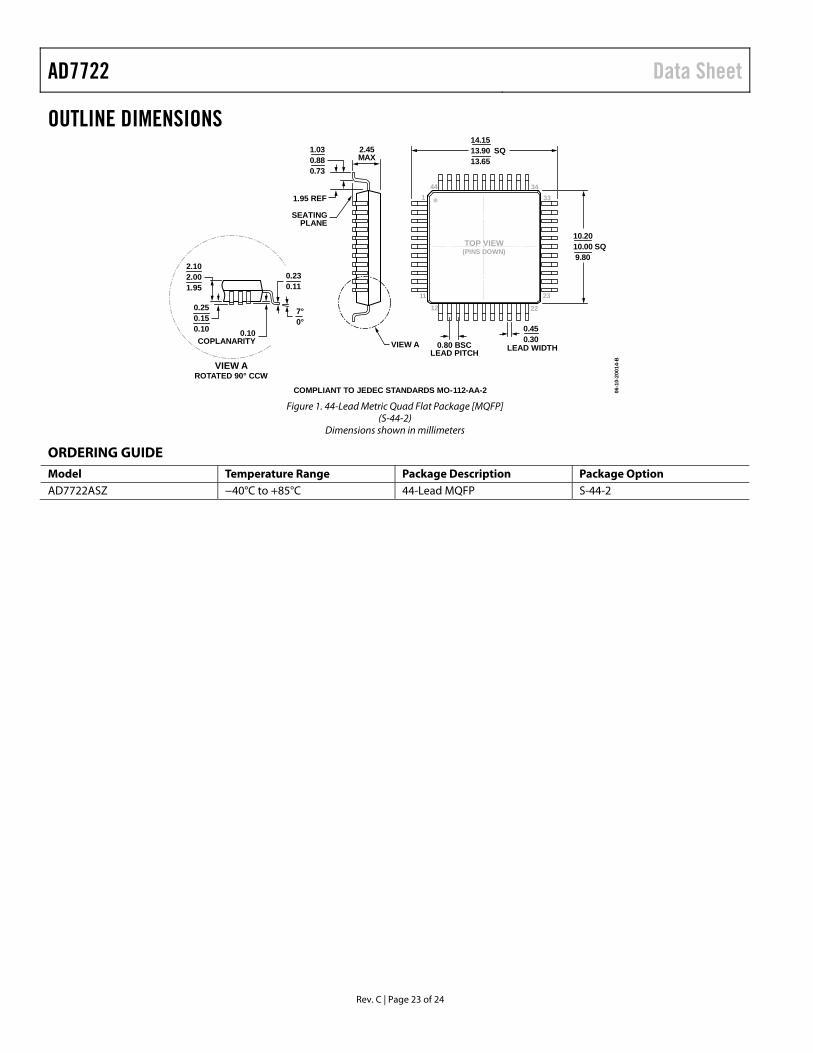
OUTLINE DIMENSIONS
COMPLIANT TO JEDEC STANDARDS MO-112-AA-2
14.1513.90 SQ13.65
0.450.30
2.45MAX
1.030.880.73
12
44
22
23
34
33
11
2.102.001.95
7°0°
0.230.11
10.2010.00 SQ 9.80
0.80 BSCLEAD PITCH
LEAD WIDTH
0.10COPLANARITY
SEATINGPLANE
1.95 REF 1
VIEW A
VIEW AROTATED 90° CCW
06-1
0-2
001
4-B
TOP VIEW(PINS DOWN)
0.250.150.10
Figure 1. 44-Lead Metric Quad Flat Package [MQFP] (S-44-2)
Dimensions shown in millimeters
ORDERING GUIDE Model Temperature Range Package Description Package Option AD7722ASZ −40°C to +85°C 44-Lead MQFP S-44-2

Data Sheet AD7722
Rev. C | Page 24 of 24
©2003–2018 Analog Devices, Inc. All rights reserved. Trademarks and registered trademarks are the property of their respective owners.
D01185-0-1/18(C)
REVISION HISTORY 1/2018—Rev. B to Rev. C Changed S-44B to S-44-2 ............................................. Throughout Changes to Ordering Guide ........................................................... 23 Updated Outline Dimensions ........................................................ 23
10/2003—Rev. A to Rev. B Changes to Ordering Guide ............................................................. 4 Replaced Figures 7 and 8 .................................................................. 7 Changes to Pin Function Descriptions ........................................... 8 Text Added to 2-Channel Multiplexed Operation Section ........ 20 Replaced Figure 25 .......................................................................... 21 Changes to Figure 29 ...................................................................... 22 Changes to Outline Dimensions ................................................... 23
5/2003—Rev. 0 to Rev. A Figures and TPCs Renumbered ....................................... Universal Changes to Absolute Maximum Ratings........................................ 4 Changes to Ordering Guide ............................................................. 4 Changes to Pin Function Descriptions .......................................... 8 Changes to Parallel Mode Pin Function Descriptions ................. 9 Changes to Serial Mode Pin Function Descriptions .................. 10 Changes to Differential Inputs Section ........................................ 15 Changes to Outline Dimensions ................................................... 23