february 2011 class v, advanced lincmos … slos710 –february 2011 class v, advanced lincmos low...
TRANSCRIPT
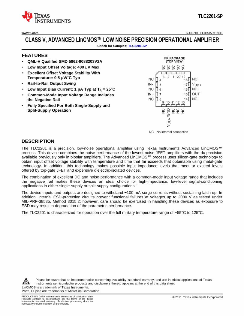
NC - No internal connection
3 2
4
5
6
7
8
18
17
16
15
14
NC
VDD+
NC
OUT
NC
NC
IN-
NC
IN+
NC
NC
NC
NC
NC
NC
NC
NC
DD
-V
NC
NC
/GN
D
FK PACKAGE(TOP VIEW)
1 20 19
9 10 11 12 13
TLC2201-SP
www.ti.com SLOS710 –FEBRUARY 2011
CLASS V, ADVANCED LinCMOS™ LOW NOISE PRECISION OPERATIONAL AMPLIFIERCheck for Samples: TLC2201-SP
1FEATURES23• QML-V Qualifed SMD 5962-9088203V2A• Low Input Offset Voltage: 400 μV Max• Excellent Offset Voltage Stability With
Temperature: 0.5 μV/°C Typ• Rail-to-Rail Output Swing• Low Input Bias Current: 1 pA Typ at TA = 25°C• Common-Mode Input Voltage Range Includes
the Negative Rail• Fully Specified For Both Single-Supply and
Split-Supply Operation
DESCRIPTIONThe TLC2201 is a precision, low-noise operational amplifier using Texas Instruments Advanced LinCMOS™process. This device combines the noise performance of the lowest-noise JFET amplifiers with the dc precisionavailable previously only in bipolar amplifiers. The Advanced LinCMOS™ process uses silicon-gate technology toobtain input offset voltage stability with temperature and time that far exceeds that obtainable using metal-gatetechnology. In addition, this technology makes possible input impedance levels that meet or exceed levelsoffered by top-gate JFET and expensive dielectric-isolated devices.
The combination of excellent DC and noise performance with a common-mode input voltage range that includesthe negative rail makes these devices an ideal choice for high-impedance, low-level signal-conditioningapplications in either single-supply or split-supply configurations.
The device inputs and outputs are designed to withstand −100-mA surge currents without sustaining latch-up. Inaddition, internal ESD-protection circuits prevent functional failures at voltages up to 2000 V as tested underMIL-PRF-38535, Method 3015.2; however, care should be exercised in handling these devices as exposure toESD may result in degradation of the parametric performance.
The TLC2201 is characterized for operation over the full military temperature range of −55°C to 125°C.
1
Please be aware that an important notice concerning availability, standard warranty, and use in critical applications of TexasInstruments semiconductor products and disclaimers thereto appears at the end of this data sheet.
2LinCMOS is a trademark of Texas Instruments.3Parts, PSpice are trademarks of MicroSim Corporation.
PRODUCTION DATA information is current as of publication date. © 2011, Texas Instruments IncorporatedProducts conform to specifications per the terms of the TexasInstruments standard warranty. Production processing does notnecessarily include testing of all parameters.

f - Frequency - Hz
TYPICAL EQUIVALENT
INPUT NOISE VOLTAGE
vs
FREQUENCY60
50
40
30
20
10
0
VDD = 5 V
RS = 20 Ω
TA = 25°CV
n -
Eq
uiv
ale
nt
Inp
ut
No
ise V
olt
ag
e -
nV
/ H
zHz
Vn
1 10 100 1 k 10 k
TLC2201-SP
SLOS710 –FEBRUARY 2011 www.ti.com
This integrated circuit can be damaged by ESD. Texas Instruments recommends that all integrated circuits be handled withappropriate precautions. Failure to observe proper handling and installation procedures can cause damage.
ESD damage can range from subtle performance degradation to complete device failure. Precision integrated circuits may be moresusceptible to damage because very small parametric changes could cause the device not to meet its published specifications.
ORDERING INFORMATION (1)
TEMPERATURE PACKAGE (2) ORDERABLE PART NUMBER TOP-SIDE MARKING
5962-9088203V2A–55°C to 125°C Tcase 20-pin FK 5962-9088203V2A TLC2201AMFKBQMLV
(1) For the most current package and ordering information, see the Package Option Addendum at the end of this document, or see the TIweb site at www.ti.com.
(2) Package drawings, thermal data, and symbolization are available at www.ti.com/packaging.
2 Submit Documentation Feedback © 2011, Texas Instruments Incorporated
Product Folder Link(s): TLC2201-SP

IN-
V -/GNDDD
TLC2201-SP
www.ti.com SLOS710 –FEBRUARY 2011
EQUIVALENT SCHEMATIC
© 2011, Texas Instruments Incorporated Submit Documentation Feedback 3
Product Folder Link(s): TLC2201-SP

TLC2201-SP
SLOS710 –FEBRUARY 2011 www.ti.com
ABSOLUTE MAXIMUM RATINGS (1)
Over operating free-air temperature range (unless otherwise noted).
VALUE UNIT
VDD Supply voltage (2), VDD- to VDD+ -8 to 8 V
VID Differential input voltage (3) ±16 V
VI Input voltage (any input) ±8 V
II Input current (each input) ±5 mA
IO Output current (each output) ±50 mA
Duration of short-circuit current at (or below) 25°C (4) Unlimited
Continuous total power dissipation See Dissipation Ratings Table
TC Operating case temperature –55 to 125 °CTstg Storage temperature –65 to 150 °C
Case temperature for 60 seconds 260 °C
(1) Stresses beyond those listed under absolute maximum ratings may cause permanent damage to the device. These are stress ratingsonly and functional operation of the device at these or any other conditions beyond those indicated under recommended operatingconditions is not implied. Exposure to absolute-maximum-rated conditions for extended periods may affect device reliability.
(2) All voltage values except differential voltages are with respect to the midpoint between VDD+ and VDD−.(3) Differential voltages are at IN+ with respect to IN−.(4) The output may be shorted to either supply. Temperature and/or supply voltages must be limited to ensure that the maximum dissipation
rating in not exceeded.
THERMAL RESISTANCE FOR FK PACKAGE (1) (2)
over operating free-air temperature range (unless otherwise noted)
PARAMETER TEST CONDITIONS MIN TYP MAX UNIT
RθJC Junction-to-case thermal resistance MIL-STD-883 test method 1012 16 °C/W
(1) Maximum power dissipation is a function of TJ (max), θJC and TC. The maximum allowable power dissipation at any allowable casetemperature is PD = (TJ (max) - TC)/θJC. Operating at the absolute maximum TJ of 150°C can affect reliability.
(2) The package thermal impedance is calculated in accordance with MIL-STD-883.
RECOMMENDED OPERATING CONDITIONSMIN MAX UNIT
VDD± Supply voltage ±2.3 ±8 V
VIC Common-mode input voltage VDD- VDD+-2.3 V
TC Operating case temperature –55 125 °C
4 Submit Documentation Feedback © 2011, Texas Instruments Incorporated
Product Folder Link(s): TLC2201-SP

TLC2201-SP
www.ti.com SLOS710 –FEBRUARY 2011
ELECTRICAL CHARACTERISTICSover operating free-air temperature range, VDD = 5 V (unless otherwise noted)
PARAMETER TEST CONDITIONS TA(1) MIN TYP MAX UNIT
25°C 80 200VIO Input offset voltage µV
Full range 400
Temperature coefficient of inputαVIO Full range 0.5 µV/°Coffset voltage
Input offset voltage long-term VIC = 0, 25°C 0.001 µV/modrift (2)RS = 50 Ω
25°C 0.5IIO Input offset current pA
Full range 500
25°C 1IIB Input bias current pA
Full range 500
Common-mode input voltageVICR RS = 50 Ω Full range 0 to 2.7 Vrange
25°C 4.7 4.8Maximum high-level outputVOH RL = 10 kΩ Vvoltage Full range 4.7
25°C 0 50Maximum low-level outputVOL IO = 0 mVvoltage Full range 50
25°C 150 315VO = 1 V to 4 V,RL = 500 kΩ Full range 75Large-signal differential voltageAVD V/mVamplification 25°C 25 55VO = 1 V to 4 V,RL = 10 kΩ Full range 10
VIC = VICRmin, 25°C 90 110CMRR Common-mode rejection ratio VO = 0, dB
Full range 85RS = 50 Ω25°C 90 110Supply voltage rejection ratiokSVR VDD = 4.6 V to 16 V dB(ΔVDD±/ΔVIO) Full range 85
25°C 1.1 1.5VO = 2.5 V,IDD Supply current mANo load Full range 1.5
VO = 0.5 V to 2.5 V, 25°C 1.8 2.5SR Slew rate at unity gain RL = 10 kΩ V/µs
Full range 1.1CL = 100 pF
f = 10 Hz 25°C 18Vn Equivalent input noise voltage nV/√Hz
f = 1 kHz 25°C 8
f = 0.1 to 1 Hz 25°C 0.5Peak-to-peak equivalent inputVn(pp) µVnoise voltage f = 0.1 to 10 Hz 25°C 0.7
In Equivalent input noise current 25°C 0.6 fA/√Hz
f = 10 kHz,Gain-bandwidth product RL = 10 kΩ, 25°C 1.8 MHz
CL = 100 pF
RL = 10 kΩ,φm Phase margin at unity gain 25°C 45°CL = 100 pF
(1) Full range is −55°C to 125°C.(2) Typical values are based on the input offset voltage shift observable through 168 hours of operating life test at TA = 150°C extrapolated
to TA = 25°C using the Arrhenius equation and assuming an activation energy of 0.96 eV.
© 2011, Texas Instruments Incorporated Submit Documentation Feedback 5
Product Folder Link(s): TLC2201-SP

TLC2201-SP
SLOS710 –FEBRUARY 2011 www.ti.com
ELECTRICAL CHARACTERISTICSover operating free-air temperature range, VDD = ±5 V (unless otherwise noted)
PARAMETER TEST CONDITIONS TA(1) MIN TYP MAX UNIT
25°C 80 200VIO Input offset voltage µV
Full range 400
Temperature coefficient of inputαVIO Full range 0.5 µV/°Coffset voltage
Input offset voltage long-term VIC = 0, 25°C 0.001 µV/modrift (2)RS = 50 Ω
25°C 0.5IIO Input offset current pA
Full range 500
25°C 1IIB Input bias current pA
Full range 500
Common-mode input voltage -5 toVICR RS = 50 Ω Full range Vrange 2.7
25°C 4.7 4.8Maximum positive peak outputVOM+ Vvoltage swing Full range 4.7RL = 10 kΩ
25°C -4.7 -4.9Maximum negative peak outputVOM- Vvoltage swing Full range -4.7
25°C 400 560VO = ±4 V,RL = 500 kΩ Full range 200Large-signal differential voltageAVD V/mVamplification 25°C 90 100VO = ±4 V,RL = 10 kΩ Full range 45
VIC = VICRmin, 25°C 90 115CMRR Common-mode rejection ratio VO = 0, dB
Full range 85RS = 50 Ω25°C 90 110Supply voltage rejection ratiokSVR VDD = ±2.3 V to ±8 V dB(ΔVDD±/ΔVIO) Full range 85
25°C 1.1 1.5VO = 0 V,IDD Supply current mANo load Full range 1.5
VO = ±2.3 V, 25°C 2 2.7SR Slew rate at unity gain RL = 10 kΩ V/µs
Full range 1.3CL = 100 pF
f = 10 Hz 25°C 18Vn Equivalent input noise voltage nV/√Hz
f = 1 kHz 25°C 8
f = 0.1 to 1 Hz 25°C 0.5Peak-to-peak equivalent inputVn(pp) µVnoise voltage f = 0.1 to 10 Hz 25°C 0.7
In Equivalent input noise current 25°C 0.6 fA/√Hz
f = 10 kHz,Gain-bandwidth product RL = 10 kΩ, 25°C 1.9 MHz
CL = 100 pF
RL = 10 kΩ,φm Phase margin at unity gain 25°C 48°CL = 100 pF
(1) Full range is −55°C to 125°C.(2) Typical values are based on the input offset voltage shift observable through 168 hours of operating life test at TA = 150°C extrapolated
to TA = 25°C using the Arrhenius equation and assuming an activation energy of 0.96 eV.
6 Submit Documentation Feedback © 2011, Texas Instruments Incorporated
Product Folder Link(s): TLC2201-SP
2 kW
V +DD
V -/GNDDD
20 W 20 W
+
-
10 kW
100 W+
-
V -/GNDDD
+
-
+
-
TLC2201-SP
www.ti.com SLOS710 –FEBRUARY 2011
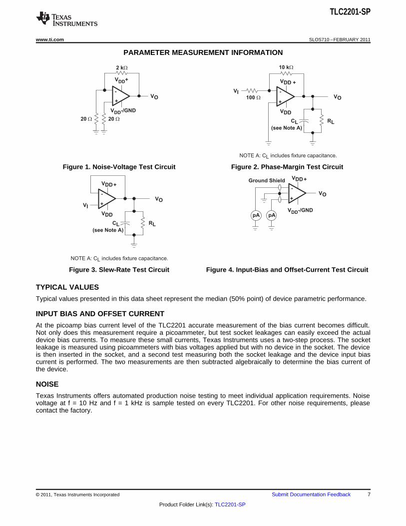
PARAMETER MEASUREMENT INFORMATION
Figure 1. Noise-Voltage Test Circuit Figure 2. Phase-Margin Test Circuit
Figure 3. Slew-Rate Test Circuit Figure 4. Input-Bias and Offset-Current Test Circuit
TYPICAL VALUES
Typical values presented in this data sheet represent the median (50% point) of device parametric performance.
INPUT BIAS AND OFFSET CURRENT
At the picoamp bias current level of the TLC2201 accurate measurement of the bias current becomes difficult.Not only does this measurement require a picoammeter, but test socket leakages can easily exceed the actualdevice bias currents. To measure these small currents, Texas Instruments uses a two-step process. The socketleakage is measured using picoammeters with bias voltages applied but with no device in the socket. The deviceis then inserted in the socket, and a second test measuring both the socket leakage and the device input biascurrent is performed. The two measurements are then subtracted algebraically to determine the bias current ofthe device.
NOISE
Texas Instruments offers automated production noise testing to meet individual application requirements. Noisevoltage at f = 10 Hz and f = 1 kHz is sample tested on every TLC2201. For other noise requirements, pleasecontact the factory.
© 2011, Texas Instruments Incorporated Submit Documentation Feedback 7
Product Folder Link(s): TLC2201-SP

TLC2201-SP
SLOS710 –FEBRUARY 2011 www.ti.com
TYPICAL CHARACTERISTICS
Table of GraphsFIGURE
VIO Input offset voltage Distribution Figure 5
vs Common-mode input voltage Figure 6IIB Input bias current
vs Free-air temperature Figure 7
vs Output curre Figure 8VOM Maximum peak output voltage
vs Free-air temperature Figure 9
VO(PP) Maximum peak-to-peak output voltage vs Frequency Figure 10
vs Frequency Figure 11
VOH High-level output voltage vs High-level output current Figure 12
vs Free-air temperature Figure 13
vs Low-level output current Figure 14VOL Low-level output voltage
vs Free-air temperature Figure 15
vs Frequency Figure 16AVD Large-signal differential voltage amplification
vs Free-air temperature Figure 17
vs Supply voltage Figure 18IOS Short-circuit output current
vs Free-air temperature Figure 19
CMRR Common-mode rejection ratio vs Frequency Figure 20
vs Supply voltage Figure 21IDD Supply current
vs Free-air temperature Figure 22
Figure 23Small signal
Figure 24Pulse response
Figure 25Large signal
Figure 26
vs Supply voltage Figure 27SR Slew rate
vs Free-air temperature Figure 28
0.1 Hz to 1 Hz Figure 29Noise voltage (referred to input)
0.1 Hz to 10 Hz Figure 30
vs Supply voltage Figure 31Gain-bandwidth product
vs Free-air temperature Figure 32
vs Supply voltage Figure 33φm Phase margin
vs Free-air temperature Figure 34
Phase shift vs Frequency Figure 16
8 Submit Documentation Feedback © 2011, Texas Instruments Incorporated
Product Folder Link(s): TLC2201-SP

Pe
rce
nta
ge
of
Un
its
- %
-500 -300 -100 100 300 500
V - Input Offset Voltage - VIO m
-5 -4 -3 -2 -1 0 1 2 3 4 5
V - Common-Mode Input Voltage - VIC
10
8
6
4
2
0
-2
-4
-6
-8
-10
I-
Inp
ut
Bia
s C
urr
en
t -
pA
IB
T - Free-Air Temperature - °CA
I-
Inp
ut
Bia
s C
urr
en
t -
pA
IB
VOM-
|I | - Output Current - mAO
|V|
- M
axim
um
Peak O
utp
ut
vo
ltag
e -
VO
M
TLC2201-SP
www.ti.com SLOS710 –FEBRUARY 2011
TYPICAL CHARACTERISTICSINPUT BIAS CURRENT
vsINPUT OFFSET VOLTAGE DISTRIBUTION COMMON-MODE INPUT VOLTAGE
Figure 5. Figure 6.
INPUT BIAS CURRENT (1) MAXIMUM PEAK OUTPUT VOLTAGEvs vs
FREE-AIR TEMPERATURE OUTPUT CURRENT
Figure 7. Figure 8.
(1) Data at high and low temperatures are applicable only within the rated operating free-air temperature ranges of the various devices.
© 2011, Texas Instruments Incorporated Submit Documentation Feedback 9
Product Folder Link(s): TLC2201-SP

R = 10 kL W
f - Frequency - HzV
- M
axim
um
Peak-t
o-P
eak O
utp
ut
Vo
ltag
e -
VO
(PP
)T - Free-Air Temperature - °CA
R = 10 kL W
VOM-
|V|
- M
ax
imu
m P
ea
k O
utp
ut
vo
lta
ge
- V
OM
6
4
2
0
-2
-4
-6
-75 -50 -25 0 25 50 75 100 125
VDD
V -2DD
V -4DD
V -6DD
V -8DD
V -10DD
V -12DD
V -14DD
V -16DD
I - High-Level Output Current - mAOH
V-
Hig
h-L
ev
el
Ou
tpu
t V
olt
ag
e -
VO
H
R = 10 kL W
V-
Hig
h-L
ev
el
Ou
tpu
t V
olt
ag
e -
VO
H
f - Frequency - Hz
TLC2201-SP
SLOS710 –FEBRUARY 2011 www.ti.com
TYPICAL CHARACTERISTICS (continued)MAXIMUM PEAK OUTPUT VOLTAGE (2) MAXIMUM PEAK-TO-PEAK OUTPUT VOLTAGE
vs vsFREE-AIR TEMPERATURE FREQUENCY
Figure 9. Figure 10.
HIGH-LEVEL OUTPUT VOLTAGE HIGH-LEVEL OUTPUT VOLTAGEvs vs
FREQUENCY HIGH-LEVEL OUTPUT CURRENT
Figure 11. Figure 12.
(2) Data at high and low temperatures are applicable only within the rated operating free-air temperature ranges of the various devices.
10 Submit Documentation Feedback © 2011, Texas Instruments Incorporated
Product Folder Link(s): TLC2201-SP
V-
Lo
w-L
evel O
utp
ut
Vo
ltag
e -
VO
LI - Low-Level Output Current - mAOLT - Free-Air Temperature - °CA
V-
Hig
h-L
ev
el
Ou
tpu
t V
olt
ag
e -
VO
H
-75 -50 -25 0 25 50 75 100 125
R = 10 kL W
-20
R = 10 kL W
f - Frequency - Hz
A-
Larg
e-S
ign
al D
iffe
ren
tial
Vo
ltag
eA
mp
lifi
cati
on
- d
BV
D
Ph
ase S
hif
t
T - Free-Air Temperature - °CA
-75 -50 -25 0 25 50 75 100 125
V-
Lo
w-L
ev
el
Ou
tpu
t V
olt
ag
e -
VO
L
TLC2201-SP
www.ti.com SLOS710 –FEBRUARY 2011
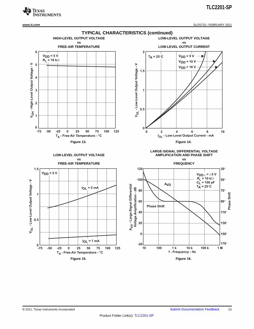
TYPICAL CHARACTERISTICS (continued)HIGH-LEVEL OUTPUT VOLTAGE LOW-LEVEL OUTPUT VOLTAGE
vs vsFREE-AIR TEMPERATURE LOW-LEVEL OUTPUT CURRENT
Figure 13. Figure 14.
LARGE-SIGNAL DIFFERENTIAL VOLTAGELOW-LEVEL OUTPUT VOLTAGE AMPLIFICATION AND PHASE SHIFT
vs vsFREE-AIR TEMPERATURE FREQUENCY
Figure 15. Figure 16.
© 2011, Texas Instruments Incorporated Submit Documentation Feedback 11
Product Folder Link(s): TLC2201-SP

12
8
4
0
-4
-8
-12
I-
Sh
ort
-Cir
cu
it O
utp
ut
cu
rren
t -
mA
SO
|V ±| - Supply Voltage - VDDT - Free-Air Temperature - °CA
-75 -50 -25 0 25 50 75 100 125
A-
La
rge
-Sig
na
l D
iffe
ren
tia
l
Vo
lta
ge
Am
pli
fic
ati
on
- d
BV
D
R = 10 kL W
R = 500 kL W
R = 500 kL W
R = 10 kL W
f - Frequency - Hz
CM
RR
- C
om
mo
n-M
od
e R
eje
cti
on
Rati
o -
dB
T - Free-Air Temperature - °CA
-75 -50 -25 0 25 50 75 100 125
15
10
5
0
-5
-10
-15
I-
Sh
ort
-Cir
cu
it O
utp
ut
cu
rre
nt
- m
AS
O
TLC2201-SP
SLOS710 –FEBRUARY 2011 www.ti.com
TYPICAL CHARACTERISTICS (continued)LARGE-SIGNAL DIFFERENTIAL VOLTAGE
AMPLIFICATION SHORT-CIRCUIT OUTPUT CURRENTvs vs
FREE-AIR TEMPERATURE SUPPLY VOLTAGE
Figure 17. Figure 18.
SHORT-CIRCUIT OUTPUT CURRENT COMMON-MODE REJECTION RATIOvs vs
FREE-AIR TEMPERATURE FREQUENCY
Figure 19. Figure 20.
12 Submit Documentation Feedback © 2011, Texas Instruments Incorporated
Product Folder Link(s): TLC2201-SP

|V ±| - Supply Voltage - VDD
I-
Su
pp
ly C
urr
en
t -
mA
DD
I-
Su
pp
ly C
urr
en
t -
mA
DD
T - Free-Air Temperature - °CA
-75 -50 -25 0 25 50 75 100 125
t - Time - sm
-20
V-
Ou
tpu
t V
olt
ag
e -
VO
V = ±5 V,
R = 10 k ,
C = 100 pF,
T - 25°C
DD±
L
L
A
W
V-
Ou
tpu
t V
olt
ag
e -
mV
O
100
75
50
25
0
-25
-50
-75
-100
t - Time - sm
TLC2201-SP
www.ti.com SLOS710 –FEBRUARY 2011
TYPICAL CHARACTERISTICS (continued)SUPPLY CURRENT SUPPLY CURRENT
vs vsSUPPLY VOLTAGE FREE-AIR TEMPERATURE
Figure 21. Figure 22.
VOLTAGE-FOLLOWER VOLTAGE-FOLLOWERSMALL-SIGNAL SMALL-SIGNAL
PULSE RESPONSE PULSE RESPONSE
Figure 23. Figure 24.
© 2011, Texas Instruments Incorporated Submit Documentation Feedback 13
Product Folder Link(s): TLC2201-SP
5
4
3
2
1
0
-1
-2
-3
-4
-5
V-
Ou
tpu
t V
olt
ag
e -
VO
t - Time - sm
V = ±5 V,
R = 10 k ,
C = 100 pF,
T - 25°C
DD±
L
L
A
W
-1
V-
Ou
tpu
t V
olt
ag
e -
VO
t - Time - sm
V = 5 V,
R = 10 k ,
C = 100 pF,
T - 25°C
DD
L
L
A
W
|V ±| - Supply Voltage - VDD
SR
- S
lew
Ra
te -
V/
sm
SR-R = 10 k ,
C = 100 pF,
T - 25°C
L
L
A
W
T - Free-Air Temperature - °CA
-75 -50 -25 0 25 50 75 100 125
SR
- S
lew
Ra
te -
v/
sm
SR-
V = ±5 V,
R = 10 k ,
C = 100 pF
DD±
L
L
W
TLC2201-SP
SLOS710 –FEBRUARY 2011 www.ti.com
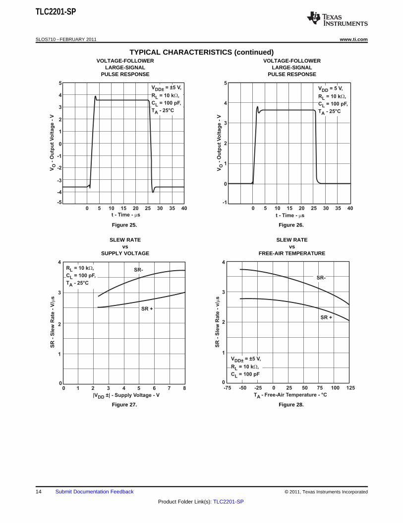
TYPICAL CHARACTERISTICS (continued)VOLTAGE-FOLLOWER VOLTAGE-FOLLOWER
LARGE-SIGNAL LARGE-SIGNALPULSE RESPONSE PULSE RESPONSE
Figure 25. Figure 26.
SLEW RATE SLEW RATEvs vs
SUPPLY VOLTAGE FREE-AIR TEMPERATURE
Figure 27. Figure 28.
14 Submit Documentation Feedback © 2011, Texas Instruments Incorporated
Product Folder Link(s): TLC2201-SP
1
0.8
0.6
0.4
0.2
0
-0.2
-0.4
-0.6
-0.8
-1
No
ise
Vo
lta
ge
-V
mt - Time - s
V = ±5 V,
f = 0.1 Hz to 10 Hz,T - 25°C
DD±
A
1
0.75
0.5
0.25
0
-0.25
-0.5
-0.75
-1
No
ise V
olt
ag
e -
Vm
t - Time - s
V = ±5 V,
f = 0.1 Hz to 1 Hz,T - 25°C
DD±
A
T - Free-Air Temperature - °CA
-75 -50 -25 0 25 50 75 100 125
Ga
in-B
an
dw
idth
Pro
du
ct
- M
Hz
f = 10 kHz,
R = 10 k ,
C = 100 pFL
L
WR = 10 k
C = 100 pF,
T - 25°C
L
L
A
W
|V | - Supply Voltage - VDD ±
Ga
in-B
an
dw
idth
Pro
du
ct
- M
Hz
TLC2201-SP
www.ti.com SLOS710 –FEBRUARY 2011
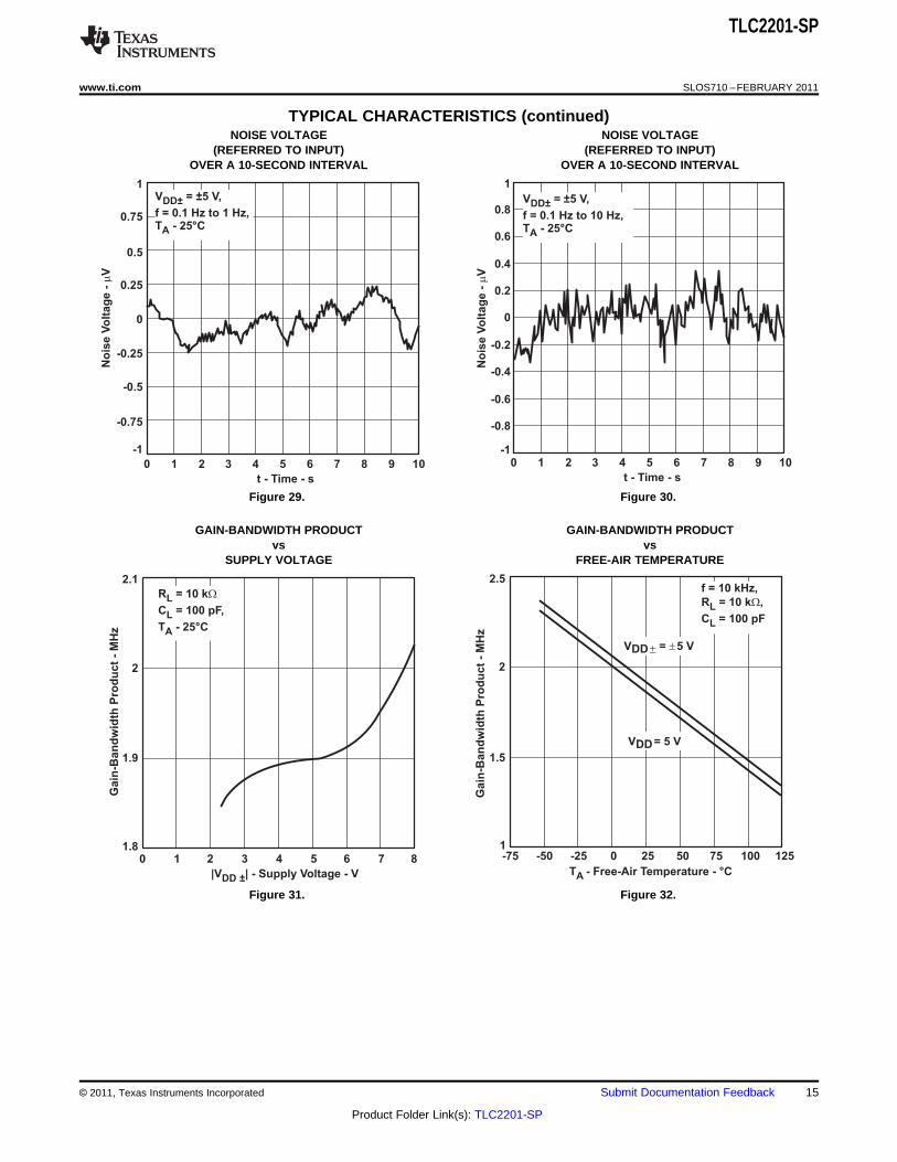
TYPICAL CHARACTERISTICS (continued)NOISE VOLTAGE NOISE VOLTAGE
(REFERRED TO INPUT) (REFERRED TO INPUT)OVER A 10-SECOND INTERVAL OVER A 10-SECOND INTERVAL
Figure 29. Figure 30.
GAIN-BANDWIDTH PRODUCT GAIN-BANDWIDTH PRODUCTvs vs
SUPPLY VOLTAGE FREE-AIR TEMPERATURE
Figure 31. Figure 32.
© 2011, Texas Instruments Incorporated Submit Documentation Feedback 15
Product Folder Link(s): TLC2201-SP

50°
48°
46°
44°
42°
40°
fm
- P
hase M
arg
in
|V | - Supply Voltage - VDD ±
R = 10 k
C = 100 pF,
T - 25°C
L
L
A
W,
50°
48°
46°
44°
42°
40°
fm
- P
hase M
arg
inT - Free-Air Temperature - °CA
-75 -50 -25 0 25 50 75 100 125
R = 10 k ,
C = 100 pFL
L
W
TLC2201-SP
SLOS710 –FEBRUARY 2011 www.ti.com
TYPICAL CHARACTERISTICS (continued)PHASE MARGIN PHASE MARGIN
vs vsSUPPLY VOLTAGE FREE-AIR TEMPERATURE
Figure 33. Figure 34.
16 Submit Documentation Feedback © 2011, Texas Instruments Incorporated
Product Folder Link(s): TLC2201-SP

TLC2201-SP
www.ti.com SLOS710 –FEBRUARY 2011
APPLICATION INFORMATION
LATCH-UP AVOIDANCE
Because CMOS devices are susceptible to latch-up due to their inherent parasitic thyristors, the TLC2201 inputsand outputs are designed to withstand −100-mA surge currents without sustaining latch-up; however, techniquesreducing the chance of latch-up should be used whenever possible. Internal protection diodes should not beforward biased in normal operation. Applied input and output voltages should not exceed the supply voltage bymore than 300 mV. Care should be exercised when using capacitive coupling on pulse generators. Supplytransients should be shunted by the use of decoupling capacitors (0.1 μF typical) located across the supply railsas close to the device as possible.
ELECTROSTATIC DISCHARGE PROTECTION
These devices use internal ESD-protection circuits that prevent functional failures at voltages at or below 2000 V.Care should be exercised in handling these devices as exposure to ESD may result in degradation of the deviceparametric performance.
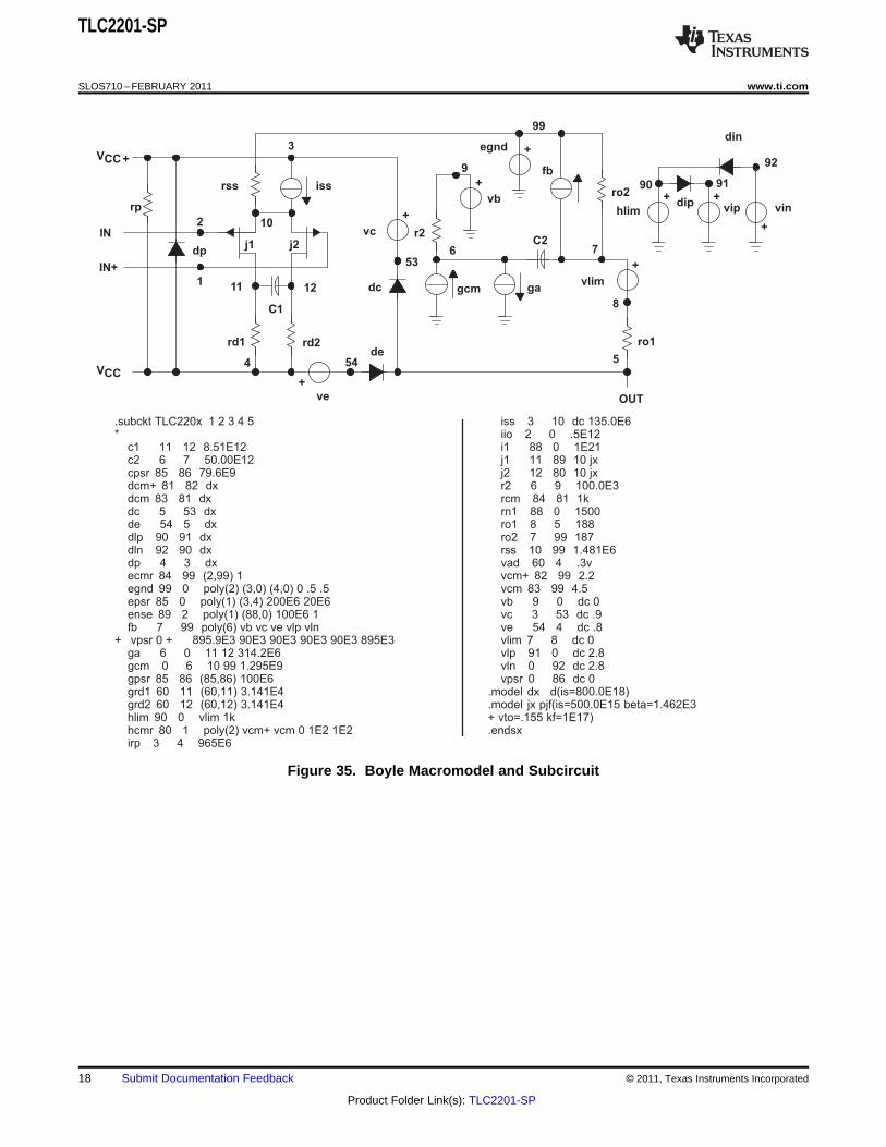
MACROMODEL INFORMATION
Macromodel information provided was derived using Microsim Parts™, the model generation software used withMicrosim PSpice™. The Boyle macromodel (3) and subcircuit in Figure 35 were generated using the TLC2201typical electrical and operating characteristics at 25°C. Using this information, output simulations of the followingkey parameters can be generated to a tolerance of 20% (in most cases):• Maximum positive output voltage swing• Maximum negative output voltage swing• Slew rate• Quiescent power dissipation• Input bias current• Open-loop voltage amplification• Unity-gain frequency• Common-mode rejection ratio• Phase margin• DC output resistance• AC output resistance• Short-circuit output current limit
(3) G. R. Boyle, B. M. Cohn, D. O. Pederson, and J. E. Solomon, “Macromodeling of Integrated Circuit Operational Amplifiers”, IEEEJournal of Solid-State Circuits, SC-9, 353 (1974).
© 2011, Texas Instruments Incorporated Submit Documentation Feedback 17
Product Folder Link(s): TLC2201-SP
TLC2201-SP
SLOS710 –FEBRUARY 2011 www.ti.com
Figure 35. Boyle Macromodel and Subcircuit
18 Submit Documentation Feedback © 2011, Texas Instruments Incorporated
Product Folder Link(s): TLC2201-SP

PACKAGE OPTION ADDENDUM
www.ti.com 25-Oct-2016
Addendum-Page 1
PACKAGING INFORMATION
Orderable Device Status(1)
Package Type PackageDrawing
Pins PackageQty
Eco Plan(2)
Lead/Ball Finish(6)
MSL Peak Temp(3)
Op Temp (°C) Device Marking(4/5)
Samples
5962-9088203V2A ACTIVE LCCC FK 20 1 TBD POST-PLATE N / A for Pkg Type -55 to 125 5962-9088203V2ATLC2201AMFKBQMLV
(1) The marketing status values are defined as follows:ACTIVE: Product device recommended for new designs.LIFEBUY: TI has announced that the device will be discontinued, and a lifetime-buy period is in effect.NRND: Not recommended for new designs. Device is in production to support existing customers, but TI does not recommend using this part in a new design.PREVIEW: Device has been announced but is not in production. Samples may or may not be available.OBSOLETE: TI has discontinued the production of the device.
(2) Eco Plan - The planned eco-friendly classification: Pb-Free (RoHS), Pb-Free (RoHS Exempt), or Green (RoHS & no Sb/Br) - please check http://www.ti.com/productcontent for the latest availabilityinformation and additional product content details.TBD: The Pb-Free/Green conversion plan has not been defined.Pb-Free (RoHS): TI's terms "Lead-Free" or "Pb-Free" mean semiconductor products that are compatible with the current RoHS requirements for all 6 substances, including the requirement thatlead not exceed 0.1% by weight in homogeneous materials. Where designed to be soldered at high temperatures, TI Pb-Free products are suitable for use in specified lead-free processes.Pb-Free (RoHS Exempt): This component has a RoHS exemption for either 1) lead-based flip-chip solder bumps used between the die and package, or 2) lead-based die adhesive used betweenthe die and leadframe. The component is otherwise considered Pb-Free (RoHS compatible) as defined above.Green (RoHS & no Sb/Br): TI defines "Green" to mean Pb-Free (RoHS compatible), and free of Bromine (Br) and Antimony (Sb) based flame retardants (Br or Sb do not exceed 0.1% by weightin homogeneous material)
(3) MSL, Peak Temp. - The Moisture Sensitivity Level rating according to the JEDEC industry standard classifications, and peak solder temperature.
(4) There may be additional marking, which relates to the logo, the lot trace code information, or the environmental category on the device.
(5) Multiple Device Markings will be inside parentheses. Only one Device Marking contained in parentheses and separated by a "~" will appear on a device. If a line is indented then it is a continuationof the previous line and the two combined represent the entire Device Marking for that device.
(6) Lead/Ball Finish - Orderable Devices may have multiple material finish options. Finish options are separated by a vertical ruled line. Lead/Ball Finish values may wrap to two lines if the finishvalue exceeds the maximum column width.
Important Information and Disclaimer:The information provided on this page represents TI's knowledge and belief as of the date that it is provided. TI bases its knowledge and belief on informationprovided by third parties, and makes no representation or warranty as to the accuracy of such information. Efforts are underway to better integrate information from third parties. TI has taken andcontinues to take reasonable steps to provide representative and accurate information but may not have conducted destructive testing or chemical analysis on incoming materials and chemicals.TI and TI suppliers consider certain information to be proprietary, and thus CAS numbers and other limited information may not be available for release.

PACKAGE OPTION ADDENDUM
www.ti.com 25-Oct-2016
Addendum-Page 2
In no event shall TI's liability arising out of such information exceed the total purchase price of the TI part(s) at issue in this document sold by TI to Customer on an annual basis.
OTHER QUALIFIED VERSIONS OF TLC2201-SP :
• Catalog: TLC2201
• Military: TLC2201M
NOTE: Qualified Version Definitions:
• Catalog - TI's standard catalog product
• Military - QML certified for Military and Defense Applications

IMPORTANT NOTICE
Texas Instruments Incorporated and its subsidiaries (TI) reserve the right to make corrections, enhancements, improvements and otherchanges to its semiconductor products and services per JESD46, latest issue, and to discontinue any product or service per JESD48, latestissue. Buyers should obtain the latest relevant information before placing orders and should verify that such information is current andcomplete. All semiconductor products (also referred to herein as “components”) are sold subject to TI’s terms and conditions of salesupplied at the time of order acknowledgment.TI warrants performance of its components to the specifications applicable at the time of sale, in accordance with the warranty in TI’s termsand conditions of sale of semiconductor products. Testing and other quality control techniques are used to the extent TI deems necessaryto support this warranty. Except where mandated by applicable law, testing of all parameters of each component is not necessarilyperformed.TI assumes no liability for applications assistance or the design of Buyers’ products. Buyers are responsible for their products andapplications using TI components. To minimize the risks associated with Buyers’ products and applications, Buyers should provideadequate design and operating safeguards.TI does not warrant or represent that any license, either express or implied, is granted under any patent right, copyright, mask work right, orother intellectual property right relating to any combination, machine, or process in which TI components or services are used. Informationpublished by TI regarding third-party products or services does not constitute a license to use such products or services or a warranty orendorsement thereof. Use of such information may require a license from a third party under the patents or other intellectual property of thethird party, or a license from TI under the patents or other intellectual property of TI.Reproduction of significant portions of TI information in TI data books or data sheets is permissible only if reproduction is without alterationand is accompanied by all associated warranties, conditions, limitations, and notices. TI is not responsible or liable for such altereddocumentation. Information of third parties may be subject to additional restrictions.Resale of TI components or services with statements different from or beyond the parameters stated by TI for that component or servicevoids all express and any implied warranties for the associated TI component or service and is an unfair and deceptive business practice.TI is not responsible or liable for any such statements.Buyer acknowledges and agrees that it is solely responsible for compliance with all legal, regulatory and safety-related requirementsconcerning its products, and any use of TI components in its applications, notwithstanding any applications-related information or supportthat may be provided by TI. Buyer represents and agrees that it has all the necessary expertise to create and implement safeguards whichanticipate dangerous consequences of failures, monitor failures and their consequences, lessen the likelihood of failures that might causeharm and take appropriate remedial actions. Buyer will fully indemnify TI and its representatives against any damages arising out of the useof any TI components in safety-critical applications.In some cases, TI components may be promoted specifically to facilitate safety-related applications. With such components, TI’s goal is tohelp enable customers to design and create their own end-product solutions that meet applicable functional safety standards andrequirements. Nonetheless, such components are subject to these terms.No TI components are authorized for use in FDA Class III (or similar life-critical medical equipment) unless authorized officers of the partieshave executed a special agreement specifically governing such use.Only those TI components which TI has specifically designated as military grade or “enhanced plastic” are designed and intended for use inmilitary/aerospace applications or environments. Buyer acknowledges and agrees that any military or aerospace use of TI componentswhich have not been so designated is solely at the Buyer's risk, and that Buyer is solely responsible for compliance with all legal andregulatory requirements in connection with such use.TI has specifically designated certain components as meeting ISO/TS16949 requirements, mainly for automotive use. In any case of use ofnon-designated products, TI will not be responsible for any failure to meet ISO/TS16949.
Products ApplicationsAudio www.ti.com/audio Automotive and Transportation www.ti.com/automotiveAmplifiers amplifier.ti.com Communications and Telecom www.ti.com/communicationsData Converters dataconverter.ti.com Computers and Peripherals www.ti.com/computersDLP® Products www.dlp.com Consumer Electronics www.ti.com/consumer-appsDSP dsp.ti.com Energy and Lighting www.ti.com/energyClocks and Timers www.ti.com/clocks Industrial www.ti.com/industrialInterface interface.ti.com Medical www.ti.com/medicalLogic logic.ti.com Security www.ti.com/securityPower Mgmt power.ti.com Space, Avionics and Defense www.ti.com/space-avionics-defenseMicrocontrollers microcontroller.ti.com Video and Imaging www.ti.com/videoRFID www.ti-rfid.comOMAP Applications Processors www.ti.com/omap TI E2E Community e2e.ti.comWireless Connectivity www.ti.com/wirelessconnectivity
Mailing Address: Texas Instruments, Post Office Box 655303, Dallas, Texas 75265Copyright © 2016, Texas Instruments Incorporated