field grading composites tailored by electrophoresis-part
TRANSCRIPT

HAL Id: hal-03266268https://hal.archives-ouvertes.fr/hal-03266268
Submitted on 21 Jun 2021
HAL is a multi-disciplinary open accessarchive for the deposit and dissemination of sci-entific research documents, whether they are pub-lished or not. The documents may come fromteaching and research institutions in France orabroad, or from public or private research centers.
L’archive ouverte pluridisciplinaire HAL, estdestinée au dépôt et à la diffusion de documentsscientifiques de niveau recherche, publiés ou non,émanant des établissements d’enseignement et derecherche français ou étrangers, des laboratoirespublics ou privés.
Field Grading Composites Tailored byElectrophoresis-Part 3: Application to Power
Electronics Modules EncapsulationSombel Diaham, Z. Valdez-Nava, T. Le, L. Lévêque, Lionel Laudebat, Thierry
Lebey
To cite this version:Sombel Diaham, Z. Valdez-Nava, T. Le, L. Lévêque, Lionel Laudebat, et al.. Field Grading CompositesTailored by Electrophoresis-Part 3: Application to Power Electronics Modules Encapsulation. IEEETransactions on Dielectrics and Electrical Insulation, Institute of Electrical and Electronics Engineers,2021, 28 (2), pp.348-354. �10.1109/TDEI.2020.009032�. �hal-03266268�

Field Grading Composites Tailored by Electrophoresis – Part 3: Application to Power Electronics Modules Encapsulation
S. Diaham1, Z. Valdez-Nava1, T. T. Le1, L. Lévêque1, L. Laudebat1,2 and T. Lebey1
1LAPLACE, Université de Toulouse, CNRS, INPT, UPS, Toulouse, France 2Université de Toulouse, INU Champollion, place de Verdun F-81012 Albi, France.
ABSTRACT
A series of three articles presents an innovative way to build advanced functionally graded materials (FGM) based on polymer/ceramic (epoxy/SrTiO3) composites tailored by electrophoresis for field grading in power electronics. In this Part 3, this method is applied in the context of power modules for DBC substrate encapsulation. An evaluation of the FGM performances is reported based on electrostatic simulations and breakdown voltage measurements on encapsulated DBC substrates. The results show a significant mitigation of the electric fringe field at the triple point while breakdown is largely increased by a factor 2 for FGM composites compared to neat epoxy. The process enables to use the electric field reinforcements of HV electrical systems (e.g. tips coming from the design), and thus potential weak points, to locally ‘self-heal’ them in-situ. Such an electrophoresis process used to build FGM composites paves the way of the next generation of functionalized polymer composites used in high voltage power applications for improving the electrical aging of insulating materials and power system reliability.
Index Terms — functionally graded materials (FGM), composite, electrophoresis, insulation, encapsulation, high voltage, field grading, power electronics modules
1 INTRODUCTION
IN power electronics, the recent and still ongoing development of high power semiconductor devices such as insulated gate bipolar transistor (IGBT) in Si [1] or metal oxide semiconductor field effect transistor (MOSFET) in SiC [2, 3] needs to be supported by higher performances packaging materials to enable higher voltage power module emergence. Among them, the encapsulation materials need to have superior electrical insulation properties (e.g. higher dielectric breakdown and partial discharge inception voltage) in order to increase the working voltage of power modules and/or to enhance their reliability. Usually, the encapsulation function is achieved using silicone gel or epoxy resin, depending on their topology. However, during high voltage (HV) operation of power modules, partial discharges and electrical treeing can occur at the triple point [4, 5], namely at the junction between the ceramic substrate, the metallization and the encapsulation, due to the very high electric field developed at that point, as shown in Figure 1. Treeing can propagate within the encapsulation or along the interface with the DBC substrate towards the grounded counter electrode [6, 7]. This triple point acts as a fringing
electrical field region [8, 9] where discharges can incept, then progressively electrically degrade the encapsulation material, up to finally fail the insulation in power modules.
The electric field divergence around the sharp edges of an HV metallization has been a well-known problem in high voltage electrical engineering for decades. A particular way to address it, from the material point of view, has been to involve field grading materials in the triple point region in order to benefit of the electrical properties of the insulator itself to reduce efficiently the field reinforcement. Even though such an approach is widely used for HV cable connectors [10], HV electrical machine and other HV apparatus [11-13], it has been rarely tried in HV power electronics modules [14-16] with a very few studies that involve composites as field grading materials.
To figure out more efficiently the electric field divergence issues, some researchers have developed field grading material concept by structuring them based on a non-homogeneous distributed composite: functionally graded materials (FGM). Among them, Okubo’s group has pioneered FGM composites with internal particle distribution gradient processed by centrifugation force for GIS applications [17, 18].
Manuscript received on 29 may 2020, in final form 30 November 2020, accepted xx Month 20yy. Corresponding author: S. Diaham

Figure 1. (a) Cross-section view of a HV power electronics module. The red circle shows the triple point location where the electric field is strongly enhanced
(see FEM modelling). (b) General electrical degradation chart leading to the dielectric breakdown.
However, for power electronics systems (as power modules) with more complex electrode design, the centrifugation process is not suitable any longer to tailor locally a property gradient exactly where the electric field is the most concentrated.
Previously, in Parts 1 and 2 of this three-articles series [19, 20], an innovative electrophoresis process was reported to build a polymer composite with a permittivity gradient (see Figure 2) that redistribute the electric field at the electrode sharp edge thanks to the self-organization of the high-k particles. In this present and last Part 3, such a concept of FGM design is applied to the encapsulation of power module substrates to evaluate its impact on the field grading efficiency and on the breakdown voltage.
Figure 2. Impact of high permittivity particles arrangement in a polymer composite on the permittivity gradient along a distance: (a) neat polymer, (b) particle homogenous distribution, (c) particle gradient distribution (FGM with gradient).
2 EXPERIMENTAL
2.1 MATERIALS AND COMPOSITE COMPOUNDS The polymer used as the host matrix is a diglycidyl ether
of bisphenol F (DGEBF) thermosetting epoxy resin. It is crosslinked using an amine-type hardener with a ratio of 10:1 (resin:hardener). The viscosity of the epoxy resin with harder is of 3000 mPa·s at room temperature and its density after curing is 1.23 g/cm3.
The high permittivity fillers used are strontium titanate (SrTiO3) particles with a density of 5.11 g/cm3 and a BET specific surface of 1.83 m2/g. They are polyhedral-shaped
and have an average diameter of 600 nm. All the details can be found in ref. [19].
The composite mixture was elaborated by a direct blending process of the SrTiO3 particles (10 vol%) into the liquid epoxy resin containing the hardener. The particles were then homogeneously dispersed within the matrix using a planetary mixer rotating at 3000 rpm for 8 minutes. The mixture was then degassed in primary vacuum (<1.5 kPa) before being poured on the electrophoretic test structures.
2.2 ELECTROPHORESIS PROCESS ON DBC SUBSTRATES
To evaluate the FGM insulation properties in the context of power electronics module’s encapsulation, the material has been applied onto direct-bounded copper (DBC) substrates with an alumina ceramic.
Figure 3. DBC substrates used during this study: top, bottom and cross-section views.
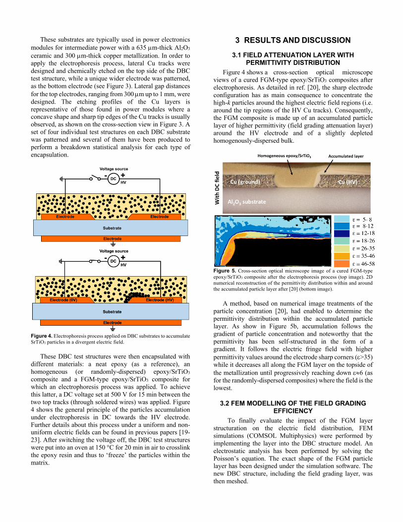
These substrates are typically used in power electronics modules for intermediate power with a 635 µm-thick Al2O3 ceramic and 300 µm-thick copper metallization. In order to apply the electrophoresis process, lateral Cu tracks were designed and chemically etched on the top side of the DBC test structure, while a unique wider electrode was patterned, as the bottom electrode (see Figure 3). Lateral gap distances for the top electrodes, ranging from 300 µm up to 1 mm, were designed. The etching profiles of the Cu layers is representative of those found in power modules where a concave shape and sharp tip edges of the Cu tracks is usually observed, as shown on the cross-section view in Figure 3. A set of four individual test structures on each DBC substrate was patterned and several of them have been produced to perform a breakdown statistical analysis for each type of encapsulation.
Figure 4. Electrophoresis process applied on DBC substrates to accumulate SrTiO3 particles in a divergent electric field.
These DBC test structures were then encapsulated with different materials: a neat epoxy (as a reference), an homogeneous (or randomly-dispersed) epoxy/SrTiO3 composite and a FGM-type epoxy/SrTiO3 composite for which an electrophoresis process was applied. To achieve this latter, a DC voltage set at 500 V for 15 min between the two top tracks (through soldered wires) was applied. Figure 4 shows the general principle of the particles accumulation under electrophoresis in DC towards the HV electrode. Further details about this process under a uniform and non-uniform electric fields can be found in previous papers [19-23]. After switching the voltage off, the DBC test structures were put into an oven at 150 °C for 20 min in air to crosslink the epoxy resin and thus to ‘freeze’ the particles within the matrix.
3 RESULTS AND DISCUSSION
3.1 FIELD ATTENUATION LAYER WITH PERMITTIVITY DISTRIBUTION
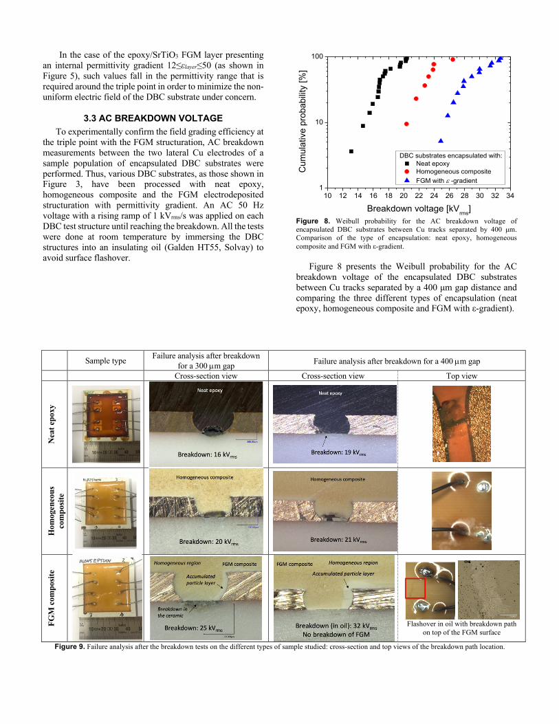
Figure 4 shows a cross-section optical microscope views of a cured FGM-type epoxy/SrTiO3 composites after electrophoresis. As detailed in ref. [20], the sharp electrode configuration has as main consequence to concentrate the high-k particles around the highest electric field regions (i.e. around the tip regions of the HV Cu tracks). Consequently, the FGM composite is made up of an accumulated particle layer of higher permittivity (field grading attenuation layer) around the HV electrode and of a slightly depleted homogenously-dispersed bulk.
Figure 5. Cross-section optical microscope image of a cured FGM-type epoxy/SrTiO3 composite after the electrophoresis process (top image). 2D numerical reconstruction of the permittivity distribution within and around the accumulated particle layer after [20] (bottom image).
A method, based on numerical image treatments of the particle concentration [20], had enabled to determine the permittivity distribution within the accumulated particle layer. As show in Figure 5b, accumulation follows the gradient of particle concentration and noteworthy that the permittivity has been self-structured in the form of a gradient. It follows the electric fringe field with higher permittivity values around the electrode sharp corners (e>35) while it decreases all along the FGM layer on the topside of the metallization until progressively reaching down e»6 (as for the randomly-dispersed composites) where the field is the lowest.
3.2 FEM MODELLING OF THE FIELD GRADING EFFICIENCY
To finally evaluate the impact of the FGM layer structuration on the electric field distribution, FEM simulations (COMSOL Multiphysics) were performed by implementing the layer into the DBC structure model. An electrostatic analysis has been performed by solving the Poisson’s equation. The exact shape of the FGM particle layer has been designed under the simulation software. The new DBC structure, including the field grading layer, was then meshed.

N
eat e
poxy
Hom
ogen
eous
co
mpo
site
FGM
with
ε -
grad
ient
Figure 6. Cross-section optical microscope images of cured neat epoxy, randomly-dispersed composite and FGM composite with accumulated particles layer. FEM simulations of the electric field under 6.5 kV: 2D cartography and 1D profile along the interface from the triple point.
For a more accurate analysis near the curved lines, the mesh was refined in these zones with a variable quadratic tetrahedral element for a more precise representation of the corner’s shape and tips [24]. Around the triple point zone, the mesh was refined to allow the calculation of the electric field every 0.4 μm. The mesh was kept constant for all simulations and permittivity was adjusted for the different cases (more details can be found in [20]). The applied potential on the metallization covered by the FGM layer was 6.5 kV while the non-covered and counter electrodes were both grounded. For convenient reasons, the FGM layer was defined by a constant permittivity and this latter was varied from low to high values for the entire layer.
Figure 6 shows the 2D electric field cartography and 1D cutline field profile for neat epoxy, homogeneous composite and FGM epoxy/SrTiO3 composite with a layer permittivity value of εlayer=50 (set as constant in the entire layer for more convenience). In the cases of neat epoxy (εbulk=4.5) and homogeneous epoxy/SrTiO3 composite (εbulk=6.5), one electric field reinforcement peak appears at the triple point and another at the top corner of the metallization. The cutline profiles along the ceramic/encapsulation interface (at 1 μm above) show the fringing electric field magnitudes at the triple point. The homogeneous composite with higher permittivity enables to decrease the electric field peak by 20% compared to epoxy. On the other hand, in the presence of the FGM layer with higher permittivity than that of the bulk (εlayer>εbulk), field mitigation occurs. Firstly, the top corner field peak almost disappears due to the layer permittivity. Secondly, the triple point fringe field is now split into two peaks each of lower magnitude.
Figure 7 summarizes the maximum electric field dependency versus the FGM layer permittivity variation. As said above, the homogeneous composite already participates to attenuate the electric field peak magnitude. However, the maximum electric field can be further mitigated in the case of the FGM composites. Particularly, an optimal permittivity range for the FGM layer has been identify for 15≤εlayer≤50 wherein the electric field is reduced by ≥50% with a minimum for 25≤εlayer≤30.
Figure 7. Maximum electric field and normalized field attenuation as a function of the FGM layer permittivity (voltage: 6.5 kV).
Noteworthy that a too high εlayer≥100 induces an undesired field grading effect by re-increasing the peak field magnitude at the FGM layer/bulk interface.
0.25 0.20 0.15 0.10 0.05 0.000
20
40
60
80
100
120
140
160
180
200
220
ebulk = 4.5
F [k
V/m
m]
Distance from triple point [mm]
0.25 0.20 0.15 0.10 0.05 0.000
20
40
60
80
100
120
140
160
180
200
220
ebulk = 6.5
F [k
V/m
m]
Distance from triple point [mm]
0.25 0.20 0.15 0.10 0.05 0.000
20
40
60
80
100
120
140
160
180
200
220
elayer = 50
ebulk = 6.5
F [k
V/m
m]
Distance from triple point [mm]
1 10 10060
80
100
120
140
160
180
200
0.3
0.4
0.5
0.6
0.7
0.8
0.9
1.0
FGM composite range
Nor
mal
ized
fiel
d at
tenu
atio
n
Max
imum
ele
ctric
fiel
d F m
ax [k
V/m
m]
Particle layer permittivity elayer
ebulk = 6.5
Neat epoxy
Homogeneouscomposite(10 vol%)
In the case of the epoxy/SrTiO3 FGM layer presenting an internal permittivity gradient 12≤εlayer≤50 (as shown in Figure 5), such values fall in the permittivity range that is required around the triple point in order to minimize the non-uniform electric field of the DBC substrate under concern.
3.3 AC BREAKDOWN VOLTAGE To experimentally confirm the field grading efficiency at
the triple point with the FGM structuration, AC breakdown measurements between the two lateral Cu electrodes of a sample population of encapsulated DBC substrates were performed. Thus, various DBC substrates, as those shown in Figure 3, have been processed with neat epoxy, homogeneous composite and the FGM electrodeposited structuration with permittivity gradient. An AC 50 Hz voltage with a rising ramp of 1 kVrms/s was applied on each DBC test structure until reaching the breakdown. All the tests were done at room temperature by immersing the DBC structures into an insulating oil (Galden HT55, Solvay) to avoid surface flashover.
Figure 8. Weibull probability for the AC breakdown voltage of encapsulated DBC substrates between Cu tracks separated by 400 μm. Comparison of the type of encapsulation: neat epoxy, homogeneous composite and FGM with ε-gradient.
Figure 8 presents the Weibull probability for the AC
breakdown voltage of the encapsulated DBC substrates between Cu tracks separated by a 400 μm gap distance and comparing the three different types of encapsulation (neat epoxy, homogeneous composite and FGM with ε-gradient).
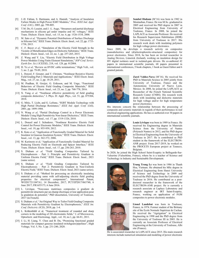
Sample type Failure analysis after breakdown for a 300 µm gap Failure analysis after breakdown for a 400 µm gap
Cross-section view Cross-section view Top view
Nea
t epo
xy
Hom
ogen
eous
co
mpo
site
FGM
com
posit
e
Flashover in oil with breakdown path
on top of the FGM surface
Figure 9. Failure analysis after the breakdown tests on the different types of sample studied: cross-section and top views of the breakdown path location.
10 12 14 16 18 20 22 24 26 28 30 32 341
10
100
DBC substrates encapsulated with: Neat epoxy Homogeneous composite FGM with e -gradient
Cum
ulat
ive
prob
abilit
y [%
]
Breakdown voltage [kVrms]
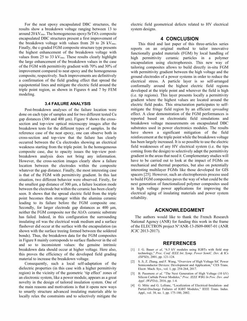
For the neat epoxy encapsulated DBC structures, the results show a breakdown voltage ranging between 13 to around 20 kVrms. The homogeneous epoxy/SrTiO3 composite encapsulated DBC structures present a first improvement of the breakdown voltage with values from 20 to 26 kVrms. Finally, the ε-graded FGM composite structure type presents the highest enhancement of the breakdown voltage with values from 25 to 33 kVrms. These results clearly highlight the large enhancement of the breakdown values in the case of the FGM with permittivity gradient with 70% and 30% of improvement compared to neat epoxy and the homogeneous composite, respectively. Such improvements are definitively a confirmation of the field grading effect that spread the equipotential lines and mitigate the electric field around the triple point region, as shown in Figures 6 and 7 by FEM modeling.
3.4 FAILURE ANALYSIS Post-breakdown analyses of the failure location were
done on each type of samples and for two different tested Cu gap distances (300 and 400 μm). Figure 9 shows the cross-section and top-view optical microscopy images after the breakdown tests for the different types of samples. In the reference case of the neat epoxy, one can observe both in cross-section and top-view that the failure has clearly occurred between the Cu electrodes showing an electrical weakness starting from the triple point. In the homogeneous composite case, due to opacity issues the top-view post-breakdown analysis does not bring any information. However, the cross-section images clearly show a failure location between the electrodes within the composite whatever the gap distance. Finally, the most interesting case is that of the FGM with permittivity gradient. In this last situation, two different behavior were observed. Firstly, for the smallest gap distance of 300 μm, a failure location mode between the electrode but within the ceramic has been clearly seen. It shows that the spread electric field from the triple point becomes then stronger within the alumina ceramic leading to its failure before the FGM composite one. Secondly, for larger electrode gap distances as 400 μm, neither the FGM composite nor the Al2O3 ceramic substrate has failed. Indeed, in this configuration the surrounding insulating oil was the electrical weak medium and a surface flashover did occur at the surface with the encapsulation (as shown with the surface treeing formed between the soldered bonds). Thus, the breakdown data for the FGM composites in Figure 8 mainly corresponds to surface flashover in the oil and so to inconsistent values: the genuine intrinsic breakdown data should occur at higher voltage. Here also, this proves the efficiency of the developed field grading material to increase the breakdown voltage.
Consequently, such a local self-adaptation of the dielectric properties (in this case with a higher permittivity region) in the vicinity of the geometric ‘tip effect’ zones of an electronic system, like a power module, appears as a great novelty in the design of tailored insulation system. One of the main reasons and motivations is that it opens new ways to smartly structure advanced insulating materials able to locally relax the constraints and to selectively mitigate the
electric field geometrical defects related to HV electrical system designs.
4 CONCLUSION
This third and last paper of this three-articles series reports on an original method to tailor innovative functionally graded materials (FGM) by local handling of high permittivity ceramic particles in a polymer encapsulation using electrophoresis. This new way of tailoring composites allows to build directly in-situ FGM with permittivity gradient between the high voltage and the ground electrodes of a power systems in order to reduce the electrical stress. A particle layer is so self-arranged conformally around the highest electric field regions developed at the triple point and wherever the field is high (i.e. tip regions). This layer presents locally a permittivity gradient where the highest values are located around the electric field peaks. This structuration participates to self-mitigate the fringe field region by an efficient spreading effect. A clear demonstration of the FGM performances is reported based on electrostatic field simulations and breakdown voltage measurements on encapsulated DBC substrates used in power electronics modules. The results have shown a significant mitigation of the field reinforcement at the triple point while the breakdown voltage has been largely increased. It is so possible to use the electric field weaknesses of any HV electrical system (i.e. the tips coming from the design) to selectively adapt the permittivity gradient in the areas that need it. Complementary studies will have to be carried out to look at the impact of FGMs on mechanical and thermal properties, but also on potentially interesting multilayer FGMs like those developed for GIS spacers [25]. However, such an electrophoresis process used to build FGM composites paves the way of what could be the next generation of functionalized polymer composites used in high voltage power applications for improving the electrical aging of insulating materials and power system reliability.
ACKNOWLEDGMENT The authors would like to thank the French Research
National Agency (ANR) for funding this work in the frame of the ELECTRON project N°ANR-13-JS09-0007-01 (ANR JCJC 2013-2017).
REFERENCES [1] J. G. Bauer et al, “6.5 kV modules using IGBTs with field stop
technology,” Proc. Conf. IEEE Int. Symp. Power SemiC. Dev. & ICs (ISPSD), 2001, pp. 121-124.
[2] S. Ji, Z. Zhang, and F. Wang, “Overview of High Voltage SiC Power Semiconductor Devices: Development and Application,” CES Trans. Electr. Mach. Sys., vol. 1, pp. 254-264, 2017.
[3] B. Passmore et al, “The Next Generation of High Voltage (10 kV) Silicon Carbide Power Modules,” Proc. IEEE WBG In Pow. Dev. and Appl. (WiPDA), 2016, pp. 1-4.
[4] G. Mitic and G. Lefranc, “Localization of Electrical-Insulation- and Partial-Discharge Failures of IGBT Modules,” IEEE Trans. Indus. Appl., vol. 38, no. 1, pp. 175-180, 2002.
[5] J.-H. Fabian, S. Hartmann, and A. Hamidi, “Analysis of Insulation
Failure Modes in High Power IGBT Modules,” Proc. IEEE Ind. Appl. Conf. (IAC), 2005, pp. 799-805.
[6] T.M. Do, O. Lesaint, and J. -L. Auge, “Streamers and partial discharge mechanisms in silicone gel under impulse and AC voltages,” IEEE Trans. Dielectr. Electr. Insul., vol. 15, no. 6, pp. 1526-1534, 2008.
[7] M. Sato et al, “Dynamic Potential Distributions of Surface Discharge in Silicone Gel,” IEEE Trans. Dielectr. Electr. Insul., vol. 22, pp. 1733-1738, 2015.
[8] C. F. Bayer et al, “Simulation of the Electric Field Strength in the Vicinity of Metallization Edges on Dielectric Substrates,” IEEE Trans. Dielectr. Electr. Insul., vol. 22, no. 1, pp. 257-265, 2015.
[9] Z. Wang and Y. Liu, “Electric Field Distribution in High Voltage Power Modules Using Finite Element Simulations,” IOP Conf. Series: Earth Env. Sci.( ICEESE), 218, vol. 128, pp. 012084.
[10] H. Ye et al, “Review on HVDC cable terminations,” High Volt., vol. 3, no. 2, pp. 79-89, 2018.
[11] L. Donzel, F. Greuter, and T. Christen, “Nonlinear Resistive Electric Field Grading Part 2: Materials and Applications,” IEEE Electr. Insul. Mag., vol. 27, no. 2, pp. 18-29, 2011.
[12] M. Pradhan, H. Greijer, G. Eriksson, and M. Unge, “Functional Behaviors of Electric Field Grading Composite Materials,” IEEE Trans. Dielectr. Electr. Insul., vol. 23, no. 2, pp. 768-778, 2016.
[13] X. Yang et al, “Nonlinear effective permittivity of field grading composite dielectrics,” J. Phys. D: Appl. Phys., vol. 51, pp. 075304, 2018.
[14] G. Mitic, T. Licht, and G. Lefranc, “IGBT Module Technology with High Partial Discharge Resistance,” IEEE Ind. Appl. Conf. (IAS), 2001, pp. 1899-1904.
[15] N. Wang et al, “Partial Discharge Control in a Power Electronic Module Using High Permittivity Non-linear Dielectrics,” IEEE Trans. Dielectr. Electr. Insul., vol. 17, pp. 1319-1326, 2010.
[16] L. Donzel and J. Schuderer, “Nonlinear Resistive Electric Field Control for Power Electronic Modules,” IEEE Trans. Dielectr. Electr. Insul., vol. 19, pp. 955-959, 2012.
[17] K. Kato et al, “Application of Functionally Graded Material for Solid Insulator in Gaseous Insulation System,” IEEE Trans. Dielectr. Electr. Insul., vol. 13, pp. 362-372, 2006.
[18] M. Kurimoto et al, “Application of Functionally Graded Material for Reducing Electric Field on Electrode and Spacer Interface,” IEEE Trans. Dielectr. Electr. Insul., vol. 17, pp. 256-263, 2010.
[19] S. Diaham et al, “Field Grading Composites Tailored by Electrophoresis – Part 1: Principle and Permittivity Gradient in Uniform Electric Field,” IEEE Trans. Dielectr. Electr. Insul., 2021 (same series).
[20] S. Diaham et al, “Field Grading Composites Tailored by Electrophoresis – Part 2: Permittivity Gradient in Non-Uniform Electric Field,” IEEE Trans. Dielectr. Electr. Insul, 2021 (same series).
[21] S. Diaham et al, “Method for processing an electrically insulating material providing same with self-adjusting electric field grading properties for electrical components”, International Patent, WO2017211847A1, 14 December, 2017; PCT/EP2017/063740, 6 June 2017; FR1655173, 6 June 2016.
[22] L. Lévêque, “Nouveaux matériaux composites à gradient de permittivité structurés par un champ électrique et leur application pour la gradation de potentiel,” PhD dissertation, University of Toulouse, 2017 (in French).
[23] S. Diaham et al, “An Original Way to Tailor Field Grading Composite Materials with Permittivity Gradient by Electrophoresis,” IEEE Int. Conf. Dielectric (ICD), 2018, pp. 1-4.
[24] L. Krähenbühl et al, “Numerical treatment of rounded and sharp corners in the modeling of 2D electrostatic fields,” J. of Microwaves, Optoelectr. and Electromag. Appl., vol. 10, no.1, pp. 66-81, 2011.
[25] J. Li, H. Liang, Y. Chen and B. Du, “Promising functional graded materials for compact gaseous insulated switchgears/pipelines”, High Voltage, Vol. 5, No. 3, pp. 231-240, 2020.
Sombel Diaham (M’16) was born in 1982 in Montauban, France. He was M.Sc. graduated in 2005 and received his PhD degree in 2007 in Electrical Engineering from University of Toulouse, France. In 2008, he joined the LAPLACE as Associate Professor. He received his Research Supervision Habilitation (HDR) from University of Toulouse in 2017. His research work deals with insulating polymers for high voltage power electronics.
Since 2009, he develops a research activity on composites (nanodielectrics and (di)electrophoretic-structured composites) for power electronics. Since 2018, he has been an invited researcher in Analog Devices, Limerick (Ireland), working on insulation design for HV digital isolators used in isolated-gate drivers. He co-authored 42 papers in international scientific journals, 68 papers presented in international conferences, 5 book chapters, 1 book as Guest Editor and 6 granted patents.
Zarel Valdez-Nava (M’16). He received his PhD in Materials Science in 2005 jointly from University of Toulouse, France and the Autonomous University of Nuevo Leon, Mexico. In 2008, he joined the LAPLACE as Researcher of the French National Scientific Research Center (CNRS). His research work deals with insulating and dielectric materials for high voltage and/or for high temperature power electronics.
His interests concern the relationship between the processing of composite and ceramic materials in regards of their performance in real electrical engineering applications. He has co-authored over 30 papers in international scientific journals.
Louis Lévêque was born in 1989 in France. He received his Engineering degree in Materials Science from the University of Nantes (Polytech Nantes) in 2012, and his PhD degree in Electrical Engineering from the University of Toulouse in 2017. He is contributed as PhD student in the framework of the ELECTRON-ANR project. From 2017-2019, he worked on the PROCETS European project at Tenneco, Belgium.
In 2020, he joined the High School Saint-Exupéry in Bellegarde-Sur-Valserine (Valserhône, France), where he is a teacher of Science and Technology in Industry and Sustainable Development.
Trung Trong Le was born in 1986 in Thanh Hoa, Vietnam. He obtained his MSc degree in Electrical Engineering from Hanoi University of Science and Technology in 2009 and received the PhD degree from the University of Toulouse in 2016. He contributed as a post-doctoral researcher in the framework of the ELECTRON-ANR project. He is currently a research associate at Laplace Laboratory and research engineer at IRT Saint-Exupéry, France, working on application of FGM composites to power electronic modules.
Lionel Laudebat was born in Toulouse, France, in 1974. Former student of the Brittany site of the Ecole Normale Supérieur de Cachan. He received the “Agrégation” in Electrical Engineering in 1998 and the PhD degree from the University of Toulouse III in 2003. He is currently an Associate Professor of Electrical Engineering at the University of Toulouse, Albi site (France).
He is associated researcher in LAPLACE since 2015. His main research interests include numerical simulation and modeling of power electronic

materials, studies of dielectric materials included modeling and characterization especially for ceramics and composite materials.
Thierry Lebey (M’98) received his M.Sc. degree in Solid State Physics in 1984, his Ph.D. in Electrical Engineering in 1989, both from University Paul Sabatier in Toulouse. Since 1990, he is engaged with the French National Scientific Research Center (CNRS) where he is now Senior Research Scientist. He is the author of more than 80 journal and 130 conference papers and holds 10 international patents.
From 2016 to 2019, he was Director of the Laboratory of Plasma and Energy Conversion - LAPLACE - in Toulouse. Since 2020, he is working as an high voltage expert for Safran Group.