for hvdc and dc grids successful fault current ... · successful fault current interruption on dc...
TRANSCRIPT
IET Power Electronics
Special Issue on Converters and Semiconductor Circuit Breakersfor HVDC and DC Grids
Successful fault current interruption on DCcircuit breaker
IET Power Electron., 2016, Vol. 9, Iss. 2, pp. 207–218This is an open access article published by the IET under the Creative Commons Attribution License(http://creativecommons.org/licenses/by/3.0/)
ISSN 1755-4535Received on 18th May 2015Revised on 20th August 2015Accepted on 13th September 2015doi: 10.1049/iet-pel.2015.0351www.ietdl.org
Yunhai Shan1, Tee C. Lim2 ✉, Barry W. Williams2, Stephen J. Finney2
1State Grid Smart Grid Research Institute, Floor 9, Building B, Future Technology Park, Changping District, Beijing 102200, People’s
Republic of China2Department of Electronic & Electrical Engineering, Institute for Energy & Environment, University of Strathclyde, Royal College Building,
204 George Street, Glasgow G1 1XW, UK
✉ E-mail: [email protected]
Abstract: This study focus on the interruption capability of the DC circuit breaker employing a current commutationapproach and evaluates the two main factors that determine the success rate for breaker current interruption, namelythe current slope di/dt before current zero and the rate of rise of the transient recovery voltage dv/dt across themechanical breaker contacts after current zero. A vacuum circuit breaker is used to evaluate DC breaker characteristics.Detailed mathematical and graphical analysis are presented for the proposed circuit operation used in analysing thecircuit breaker properties, with simulation and experimental results at fault current levels up to 330 A.
1 Introduction
Current interruption in a direct current (DC) system is more difficultthan in an alternating current (AC) system due to the absence of anatural current zero (CZ). Since there is no large inductive devicein the voltage source converter-based DC system, DC breakershave to interrupt the fault current quickly to avoid excessiveovercurrent and to dissipate the stored magnetic energy withoutproducing an excessive high voltage. Numerous proposals forintroducing CZ have been presented in articles and patentapplications [1–9]. The methodology can be divided into twogroups. The first group can be addressed as the inverse voltagemethod where the classic mechanical AC interrupter creates arcvoltage significantly in excess of the system voltage. The secondgroup can be interpreted as employing a current commutationmethod where a virtual CZ is developed by utilising auxiliarymeans which include current oscillation and voltage commutation;where the current oscillation is accomplished by switching parallelcommutation circuits to produce a counter-current through thebreaker. Voltage commutation means the current commutation isachieved by introducing a voltage which exceeds the on-statevoltage of the parallel commutation path.
Asea Brown Boveri Ltd (ABB) has proposed a hybrid DC breakerto fulfil high-voltage DC (HVDC) grid requirements [10, 11]. Thisnew hybrid configuration has negligible on-state power losses andprovides current interruption capability within 4 ms, at 70 kV.There are two parallel branches: one branch contains a seriescombination of a semiconductor-based commutation switch and afast mechanical disconnector, and the other branch is thesemiconductor-based breaker that comprises several sections eachwith individual arrester banks. Each independent section in thebreaker branch is designed for pro rata full voltage and full currentbreaking capability, whereas the load commutation switch branchis dimensioned for lower voltage and energy capability. Thedisconnecting circuit offers dielectric separation of the load afterfault clearance thereby protecting the arrester banks of the hybridHVDC breaker from thermal overload. The fast mechanical switchis opened with zero current thereby facilitating a lightweightcontact system. When the mechanical switch reaches the openposition the main HVDC breaker interrupts the current that hasbeen commutated into it. The dielectric separation means the loadcommutation switch has a low voltage requirement. Proactive
control of the hybrid HVDC breaker is utilised to compensate forthe time delay of the fast disconnector. Another method [12–15] toproduce CZ in the mechanical switch involves current oscillation.In general, this topology comprises two mechanical switches; amain breaker and an isolation switch (as with the ABB hybridbreaker); the main breaker is parallelly connected to commutationand energy absorbing paths. The main breaker supports thecontinuous current flow; the isolation switch provides dielectricseparation of the load after fault clearance thereby avoiding metaloxide varistor (MOV) thermal overload, while the solid-stateswitches in the commutation path only conduct during theinterruption process. A series combination of a capacitance C andinductance L is incorporated into the commutation path; thus therewill be an oscillating current between the main breaker andcommutation path. The line current originally flowing through themain breaker is sinusoidally transferred into the commutation path.At this point, a CZ arises in the nominal path and the mainbreaker can interrupt with zero current. As the line currentcontinues to flow through the LC commutation circuit, the voltageacross the capacitor C charges to a voltage within the capability ofthe grid. At this voltage, the remaining energy stored in the lineinductance is dissipated in the energy absorption path (MOV),forcing the line current to decrease. There are two currentcommutation modes; namely active commutation if C ispre-charged, otherwise passive commutation.
The current oscillation approach, especially active commutation,dominates the development of the hybrid HVDC breaker. Sincethe current oscillation involves an arc situation, the vacuuminterrupter becomes the prefer building block for HVDC circuitbreakers (CBs) due to its excellent insulating properties after theCZ. However, this is not the approach proposed by ABB in [10].Rather than interruption with an arc based on current oscillation,the ABB approach is interruption without an arc voltage.Assuming interruption at same power rating, the two approaches(traditional and ABB approaches) compare as follows:
† The mass of mechanical switch in the traditional approach is largecompared with the ABB approach. Therefore, the ABB openingspeed can be faster.† Since the first approach has to deal with an arc, the interruptionperformance is uncertain, unlike the ABB approach.
207
Fig. 1 Proposed unipolar test circuit and its operational sequences
a Proposed unipolar test circuitb Operational sequence of the test circuit; CZ crossing in the VCB
IET Power Electron., 2016, Vol. 9, Iss. 2, pp. 207–218208 This is an open access article published by the IET under the Creative Commons Attribution License
(http://creativecommons.org/licenses/by/3.0/)

Fig. 2 Test interruption sequences
a Pre-charging of the commutation capacitorb Activation of the fault by switching T4c Commutation of the VCB by switching T3
† The conduction power loss in the traditional approach is smaller,but both are negligible.† Both need solid-state switches in the commutation bypass path,and the traditional approach needs large capacitance.
For interruption at high power rating, the hybrid HVDC breakerproposed by ABB appears the only way to meet the requirement
IET Power Electron., 2016, Vol. 9, Iss. 2, pp. 207–218This is an open access article published by the IET under the Creative(http://creativecommons.org/licenses/by/3.0/)
of HVDC grids. However, from an economical view, the hybridHVDC breaker adopting current commutation may be moresuitable for the low- and medium-voltage applications, such aselectric traction, various drives and converter systems. This paperfocus on the interruption capability of the DC CB under a currentcommutation approach and evaluates the two main factors thatdetermine the success rate for breaker interruption, namely the
209Commons Attribution License
Table 1 Switched timing regulations
Stage Time VCB T1 T2 T3 T4
resetting the commutation circuit tnor on on Off off offt0− on off on off off
fault current introduction t0 on off off off onVCB current interruption t1 off off off off on
t2–t6 off off off on on
tnor represents a normal working period; t0− is the moment immediatelyfollowing the occurrence of the peak in the coil current; t0 represents themoment that the fault current starts to arise in the circuit; t1 representsthe moment that the VCB electrodes start to separation; and t2−t6 is thecommutation and interruption of the fault current.
current slope di/dt before CZ and the rate of rise of the transientrecovery voltage dv/dt across the mechanical breaker after CZ. Assuch, this paper is applicable to any LC resonant approach,including the self-sustaining, multi resonant cycle approach in[12–15].
Section 2 in this paper evaluates the proposed test circuit used toinvestigate the vacuum CB (VCB) characteristics. Sections 3 and 4include the simulation and experimental results that evaluate thefactors that contribute to unsuccessful and successful breakerinterruption.
2 Proposed test circuit
An accurate VCB model is complicated, since it involves manyparameters including contact material, gap distance and electrodesdimension. A small change in any parameter can result in asignificant performance change. There is no complete mathematicmodel describing all VCB properties in terms of its internalparameters. Here, the VCB will be considered as a black box,ignoring all the internal parameters, but this black box will attemptto retain the features and regular pattern of successful VCBinterruptions based on external conditions. There are two specificexternal parameters that determine this functionality; namely di/dtand dvVCB/dt, where the former represents the rate of decrease ofcurrent through the VCB immediately before a CZ and the laterrepresents the rate of increase of voltage across the VCB contactsimmediately after a CZ. For example, in obtaining a 100%successful interruption rate with fast commutation, an increase indi/dt introduces a decreased allowable dvVCB/dt. For fixed di/dt,dvVCB/dt and arcing time, the interruption probability reduces asthe interruption current increases. The di/dt and dvVCB/dt forsuccessful interruption reduce with decreasing electrode spacing[16–18]. Thus, in order to investigate VCB characteristics, aunipolar test circuit is proposed based on a VCB with active modecommutation. (Note the test circuit is not necessarily the topologythat would be used for a practical hybrid DC CB — rather thisproposed circuit is used in this paper to evaluate the VCBcharacteristics only). Fig. 1 shows the proposed unipolar testcircuit and the timing intervals for commencing a fault current andsubsequent breaker interruption (respective test interruptionsequences are shown in Fig. 2).
There are three operating sequences during the cycle.
† Pre-charging of the commutation capacitor (resetting thecommutation circuit).† Creation of the fault by load switching T4 (fault currentintroduction).† Commutation of the VCB by switching T3 (VCB currentinterruption).
The sequential timing operations for the test circuit shown inFig. 2 are tabulated in Table 1.
2.1 Pre-charging of the commutation capacitor
Fig. 2a illustrates the normal operation of the test circuit (tnor). Toinvestigate VCB properties in high-current situations, the capacitor
210 This is an open access article publi
bank (Cbank) is charged to VDC in order to supply a fault currentdetermined by the fault resistor RFAULT, which is connected inparallel with the load resistor RLOAD by switch T4. When the VCBis in an on-state (zero contact gap), a low current VDC/RLOAD issupplied by VDC. The switches T2, T3 and T4 are off and T1 is on,charging the commutation capacitor to VDC with an exponentialgrowth via the resistor R1. In this interval, the equation relatingcurrents iDC, iVCB′ and i1 is
iDC = iVCB′ + i1 (1)
where the circuit loop of i1 is VDC−D1−CC−T1−R1 which has thefollowing differential equation
1
CC
∫i1dt + i1R1 = VDC (2)
with the initial condition
VCC= 0 (V)
which yields
i1(t) =VDC
R1e(−t/t1) (A) (3)
and
VCC(t) = VDC 1− e(−t/t1)
( )(V) (4)
where t1 = R1CC
When the current i1 reduces to zero, the voltage across thecommutation capacitor CC reaches VDC, retaining this voltageprovided T1 remains on.
The circuit loop iVCB′ comprising VDC−D1−VCB−LLOAD−RLOAD
gives
LLOADdiVCB′
dt+ iVCB′RLOAD = VDC (5)
with the initial condition
iVCB′ = 0 (A)
which yields
iVCB′ t( ) = iLOAD t( ) = VDC
RLOAD1− e(−t/t2)( )
(A) (6)
where t2 = LLOAD/RLOAD
When (6) stabilises, the current iVCB′ through the VCB is equal tothe source current iDC. With large load resistance, this ‘wetting’current is small during this interval and can be neglected in thefollowing analysis.
Although the voltage VCCacross the commutation capacitorCC has
been charged to the DC source, it is not ready to introduce acounter-current through the VCB due to its voltage polarity, VCC
.The pre-charge cycle needs to be completed before the fault currentis applied. The voltage polarity of the commutation capacitor has tobe reversed before t0 at t0−. With T1 off and T2 on, the circuit loopequation for CC−VCB−LC−T2 is
1
CC
∫iT2dt + LC
diT2dt
= 0 (7)
with the initial conditions
iT2 = 0 (A) and VCC= −VDC (V)
IET Power Electron., 2016, Vol. 9, Iss. 2, pp. 207–218shed by the IET under the Creative Commons Attribution License
(http://creativecommons.org/licenses/by/3.0/)

which yield
iT2 t( ) = VDC
Zsinv0t (A) (8)
and
VCCt( ) = −VDC cosv0t (V)
0 ≤ v0t ≤ p (rad)(9)
where v0 = 1/�������LCCC
√(rad/s) and Z = ��������
LC/CC
√(V)
At ω0t = π, the current iT2 cannot reverse as the diode in series withT2 is reverse bias and the voltage VCC
across the commutationcapacitor retains a charge of −VDC.
2.2 Activation of the fault by switching T4
Fig. 2b illustrates how the fault current rises. When T4 is switchedon at t0 (with the others switches off), the energy stored in thecapacitor bank Cbank is released through the load inductor LC andfault resistor RFAULT to produce a high current through the VCBbefore the electrodes separate. The commutation circuit is asecond-order L–C–R circuit with a capacitor initial voltage of VDC.The load resistor RLOAD is ignored due to its large resistancecompared with the fault resistor RFAULT. The circuit loopcomprising Cbank−VCB−LLOAD−T4−RFAULT is expressed by
1
Cbank
iFAULT dt + LLOADdiFAULT
dt+ iFAULTRFAULT = 0 (10)
with the initial conditions
iFAULT = iVCB′ ≃ 0 (A); VCbank= −VDC (V)
Equation (10) can be divided into three different models in term ofthe relationship between RFAULT and 2
��������������LLOAD/Cbank
√.
When RFAULT . 2��������������LLOAD/Cbank
√, it is an over-damped circuit,
such that there are two unequally negative real numbers in itslatent root. Thus, it yields
iFAULT t( ) = − VDC
LLOAD P2 − P1
( ) e p1 t − e p2t( )
(A) (11)
and
VCbankt( ) = VDC
P2 − P1
( ) P2 ep1t − P1 e
p2t( )
(V) (12)
where
P1 = − RFAULT
2LLOAD+
�����������������������������RFAULT
2LLOAD
( )2
− 1
LLOADCbank
√
P2 = − RFAULT
2LLOAD−
�����������������������������RFAULT
2LLOAD
( )2
− 1
LLOADCbank
√
The capacitor bank Cbank always discharges its stored energy into thefault path. When t = 0+, iFAULT(0+) = 0; as t→∞, iFAULT(∞) = 0.Thus, the fault current must rise from zero and then decrease tozero; and time tm to reach the maximum current, is determinedfrom diFAULT/dt = 0, and is given by
tm = ln P2/P1
( )P1 − P2
(13)
Since the opening speed of the VCB is found to be about 1 m/s and
IET Power Electron., 2016, Vol. 9, Iss. 2, pp. 207–218This is an open access article published by the IET under the Creative(http://creativecommons.org/licenses/by/3.0/)
the occurrence of the arc voltage indicates the contacts of the VCBstarts to separate [9, 10], the time difference between t1 and t2determines how far the internal electrodes have separated.Independent of the discharge mode, the commutation circuitcurrent (having triggered T3) has to rise to (or exceed) the faultcurrent iFAULT(t) level at t2, in order to be able to investigate VCBinterruption properties. When the electrodes start to open at t1, theVCB experiences an arc voltage, the polarity of which depends onthe direction of the VCB current, until a successful commutationis achieved.
2.3 Commutation of the VCB by switching T3
In Fig. 2c, the commutation period t2− t3 is far shorter than the faultpath time constant, and it is assumed that the fault current iFAULT(t)isconstant within this period. T3 is fired to introduce thecounter-current flow through the VCB, forcing the fault currentthrough the VCB to zero, once the electrodes have separated to aspecific distance. During this interval, the relationship betweeniFAULT, iVCB and iT3 is given by
iFAULT = iVCB + iT3 (A) (14)
where the differential equation for iT3 is the same but with oppositedirection to iT2 during commutation and is given by
1
CC
iT3 dt + LCdiT3dt
= 0 (15)
with the initial conditions
iT3 = 0 (A) and VCC= VDC (V)
which yields
iT3 t( ) = VDC
Zsinv0t (A) (16)
and
VCCt( ) = VDC cosv0t (V)
0 ≤v0t ≤ p (rad)(17)
where v0 = 1/�������LCCC
√(rad/s) and Z = ��������
LC/CC
√(V)
With the appropriate choice of LC and CC, that is, with anappropriate selection of di/dt, a successful interruption shouldoccur as a result of the first CZ. The second CZ is utilised if thefirst interruption fails. As the auxiliary switches (T3 and T4) areuni-directional due to the series blocking diodes therebypreventing the current reversing, the counter-current introduced bythe resonant LCCC circuit can produce at most two CZs as itsamplitude exceeds the VCB current at the time of commutation,thus providing two opportunities for an interruption. Theinterruption process is considered a failure if the VCB currentcontinues after the second gap CZ (this is similar to AC breakerswhich can be specified based on two mains cycles forcommutation). It is assumed that interruption is achieved at firstCZ, which means iT3 (t3) = iFAULT(t2, t3). The time tCZ1 to the firstVCB CZ is
tCZ1 =−sin−1{iFAULT(t2)Z/VDC}
v0(18)
The timesingledollar singledollar to the second VCB CZ is
tCZ2 =p+ sin−1{iFAULT(t2)Z/VDC}
v0
211Commons Attribution License

The VCB voltage falls to and is clamped to the residual voltage of thecommutation capacitor. Thus, the fault current passing throughthe VCB is commutated into the LC−CC path; and the current iT ′
3in the circuit loop Cbank−CC−T3−LC−LLOAD−T4−RFAULT isdefined by
1
CC
∫iT ′3dt + LC
diT ′3
dt+ LLOAD
diT ′3
dt+ iT ′
3RFAULT = VDC (19)
where the voltage across Cbank can be considered a DC source due toa large Cbank with the initial conditions
iT ′3= iT3 t3
( )(A) and VC′
C= VCC
t3( )
(V )
Practically, RFAULT , 2������������LLOAD/CC
√. Thus, (19) yields
iT ′3t( ) = 2K1 e
−d2t cos v3t − u( )
(A) (20)
VC′Ct( ) = 2K1
CCv4[ cos (b2 − u)− e−d2t cos v3t − u+ b2
( )]
+ VCCt3( )
(V) (21)
where
d2 =RFAULT
2 LLOAD + LC( ) ;
v23 =
1
LLOAD + LC( )
CC
− RFAULT
2 LLOAD + LC( )
( )2
;
v4 =����������d2
2 + v23
√; b2 = tan−1 v3
d2;
K1=����������������������������������������������������������������iT3 (t3)
2
( )2
+ [{VDC−VCC(t3)}/{LLOAD+LC}]−d2iT3 (t3)
2v3
( )2√
;
and
u = tan−1 [{VDC − VCC(t3)}/{LLOAD + LC}]− d2iT3 (t3)
v3iT3 (t3)
During interval t3−t5, the current iT ′3initially increases due to the
stored magnetic energy transfer and the residual voltage on thecommutation capacitor. Then it starts to reduce, allowing diodeDFW to conduct; whence the voltage across the VCB reaches itsmaximum voltage VDC thereby forward biasing the freewheel diode.
With diode DFW forward bias, the load (the fault) is bypassed,effectively decoupling the fault from the commutation circuit.Current iT ′
3= iT ′′
3+ iFW, where iT ′′
3discharges through the circuit
loop Cbank−CC−T3−LC−DFW, transferring magnetic energy to anelectric field, causing VCC
to increase according to
1
CC
iT ′′3 dt + LCdiT ′′
3
dt= VDC (22)
with the initial conditions
iT ′′3= iT ′
3(t5) (A) and VC′′
C= VC′
C(t5) (V)
212 This is an open access article publi
which yields
iT ′′3t( ) = VDC − VC′
Ct5( )
Zsin v0t
( )+ iT ′3t5( )
cos v0t( )
(A) (23)
VC′′Ct( ) =
[VDC cos v0t
( )− VC′Ct5( )
cos v0t( )− 1
( )+ ZiT ′
3t5( )
sin v0t( )]
(24)
where v0 = 1/�������LCCC
√(rad/s) and Z = ��������
LC/CC
√(V)
The voltage VCCacross the commutation capacitor terminates with
the opposite polarity, when current iT ′′3reduces to zero. The transfer
of the stored magnetic energy in LC causes this voltage rise. The timetd, t5 to t6, is
td =1
v0tan−1 iT ′
3t5( )
Z
VDC − VCC′ t5( ) (25)
As the current iT ′′3reduces to zero at t6, the current iFW conducts
through the circuit loop LLOAD−T4−RFAULT−DFW to dissipate themagnetic energy stored in the load (fault) inductor LLOAD, whichobeys the following differential equation
LLOADdiFWdt
+ RFAULTiFW = 0 (A) (26)
with the initial conditions
iFW t6( ) = iT3 ′ t6
( )which yields
iFW t( ) = iT3 ′ t6( )
e(−t/t3)
where t3 = LLOAD/RFAULT
The analytical equations corresponding to each interval of the testcircuit have now been derived. They can be used to calculate therequired peak voltage, peak currents and the CZ time whenthe component values and conditions are known; such as when thecommutation circuit is triggered to achieve a CZ.
3 Simulation results
A typical interruption failure occurs when the counter-currentproduced by the commutation circuit is less than the fault currentdue to slow detection and triggering of the solid-state switches.That is, there is no CZ in the VCB. The commutation parametersare initially deliberately designed to result in an unsuccessfulinterruption. Fig. 3a gives the simulated results overview. Fig. 3bdepicts the simulation in more detail, and the preparation andinterruption of the test circuit. The figures on the left describe thevoltage across capacitor bank VCbank
, the commutation capacitorVCC
and the main switch VVCB. The figures on the right plot thecurrent passing through the main switch iVCB, the fault pathiFAULT, the resistor R1 path i1, the commutation T2 path iT2 and T3path iT3 . A failed interruption induced by large di/dt and dvVCB/dtcan be simulated, as shown in Figs. 3c and d. With high di/dt anddvVCB/dt, the current passing through the VCB still conducts evenif CZ points occur. The model of the VCB is seen as a shortcircuit in this situation [19, 20].
Test circuit performance during a successful interruption at thefirst CZ is shown in Fig. 4. Fig. 4a shows the overall view andFig. 4b depicts the results in detail. The waveforms on the left arevoltage profile, while current profile is on the right.
During successful interruption, the energy stored in the inductanceis transferred so as to contribute to the VCC
increase. In Fig. 4, VVCB
immediately equals VCCwhen the first CZ occurs and then tracks its
change until the free-wheel diode DFW conducts.
IET Power Electron., 2016, Vol. 9, Iss. 2, pp. 207–218shed by the IET under the Creative Commons Attribution License
(http://creativecommons.org/licenses/by/3.0/)

Fig. 3 Test circuit simulation waveforms for unsuccessful interruption
a Overview of simulated results on no CZ conditionb Detailed view on respective waveforms with no CZ conditionc Overview of simulated results on large di/dt and dVVCB/dt conditiond Detailed view on respective waveforms with large di/dt and dVVCB/dt conditionVDC = 600 V, Cbank = 7 mF, CC = 10 μF, R1 = 200 Ω, LC = 150 μH, LLOAD = 1.7 mH, RLOAD = 600 Ω, RFAULT = 4 Ω
IET Power Electron., 2016, Vol. 9, Iss. 2, pp. 207–218213This is an open access article published by the IET under the Creative Commons Attribution License
(http://creativecommons.org/licenses/by/3.0/)
Fig. 4 Test circuit simulation waveforms for successful interruption
a Overview of simulated results with first CZ conditionb Detailed view on respective waveforms with first CZ conditionVDC = 600 V, Cbank = 7 mF, CC = 10 μF, R1 = 200 Ω, LC = 150 μH, LLOAD = 1.7 mH, RLOAD = 600 Ω, RFAULT = 4 Ω
4 Experimental results
Test circuit experimentation is necessary to validate the analysis andsimulation results, and also to explore VCB interruption in terms ofexternal conditions, including di/dt and dvVCB/dt. Interruptionprobability is based on the successful interruption at either of firsttwo CZ points. To avoid system damage due to the effects ofexcessive currents, an MOV was connected across the VCB and aseries diode was located before capacitor bank (Cbank = 7 mF) toblock currents flowing back into the DC source. 600 Ω loadresistance was utilised in all the experimentation. The VCBcharacteristics are shown in Table 2.
The performance of the test circuit interrupting a 330 A faultcurrent at the first CZ is shown in Fig. 5a. After the voltage VCCacross commutation capacitor reversed and retained as described inSection 2.1, the fault current iFAULT produced by the capacitorbank voltage VCbank
is actuated and flows through the VCB beforeelectrode separation, so iFAULT = iVCB. The fault current throughthe VCB is sinusoidally displaced by the commutation circuit
Table 2 Technical data on triple pole VCBs [21]
Contactor reference CMV 15
operating voltage, kV 1.2current rating, A 150max motor duty, kW 225max transformer duty, kVA 250closing, Whold in, W
25012
weight of contactor, kg 4thermal rating (1 s), kA 4mechanical life, cycles 5 × 10⁶
214 This is an open access article publi
current iT3 , until the VCB current is zero; when iFAULT = iT3 andiVCB = 0. During this period, the voltage across the VCB (VVCB) iszero initially due to the electrodes being closed and when parting,a constant 12 V arc forms as iFAULT rises. As long as the di/dt(rate of change of the VCB current before CZ) was appropriatelydesigned or the gap distance of the VCB reaches to a specificvalue to support a large di/dt, the commutation will be successfuland the gap voltage clamps to the capacitor residual voltage VCC
,until iT3 starts to decrease (DFW conduction). VVCB has beencharged to VDC but VCC
continues to increase due to the energystored in the commutation inductor LC.
The corresponding parts of Fig. 5b show interruption at the secondgap CZ with the same interrupting current level. In this case, iVCBcontinues to flow through the VCB in the opposite direction. Thearc voltage VVCB 12 V is reverse. Finally, the interruption issuccessful at the second CZ. With successive interruption attemptsthe resonance voltage in VVCB progressively decays, sinceresistance is introduced as the plasma starts to recover. Oscillationwith the commutation inductor occurs after a successfulinterruption because of a VCB gap capacitive effect [21].
The voltage performance during an unsuccessful interruption isshown in Fig. 6a, with the corresponding current waveforms in theexpanded view. Interruption failure occurrence is random;sometimes, even with successful interruption conditions at the firstor second CZ, failure occurs without any electrical visualindication, as shown in Figs. 6a and b. The reason for re-ignitionis that there is no vacuum state in the vacuum interrupter after CZor parts of the contacts are still able to emit vapour because of ahot spot on electrode surface after experiencing the arc. In otherwords, the arc starts to recover as its current is reduced, butrecovery speed is determined by a recovery rate. For a given gap,if di/dt is slightly more than the recovery rate, interruption ispossible. However, if di/dt significantly exceeds the recovery rate,
IET Power Electron., 2016, Vol. 9, Iss. 2, pp. 207–218shed by the IET under the Creative Commons Attribution License
(http://creativecommons.org/licenses/by/3.0/)
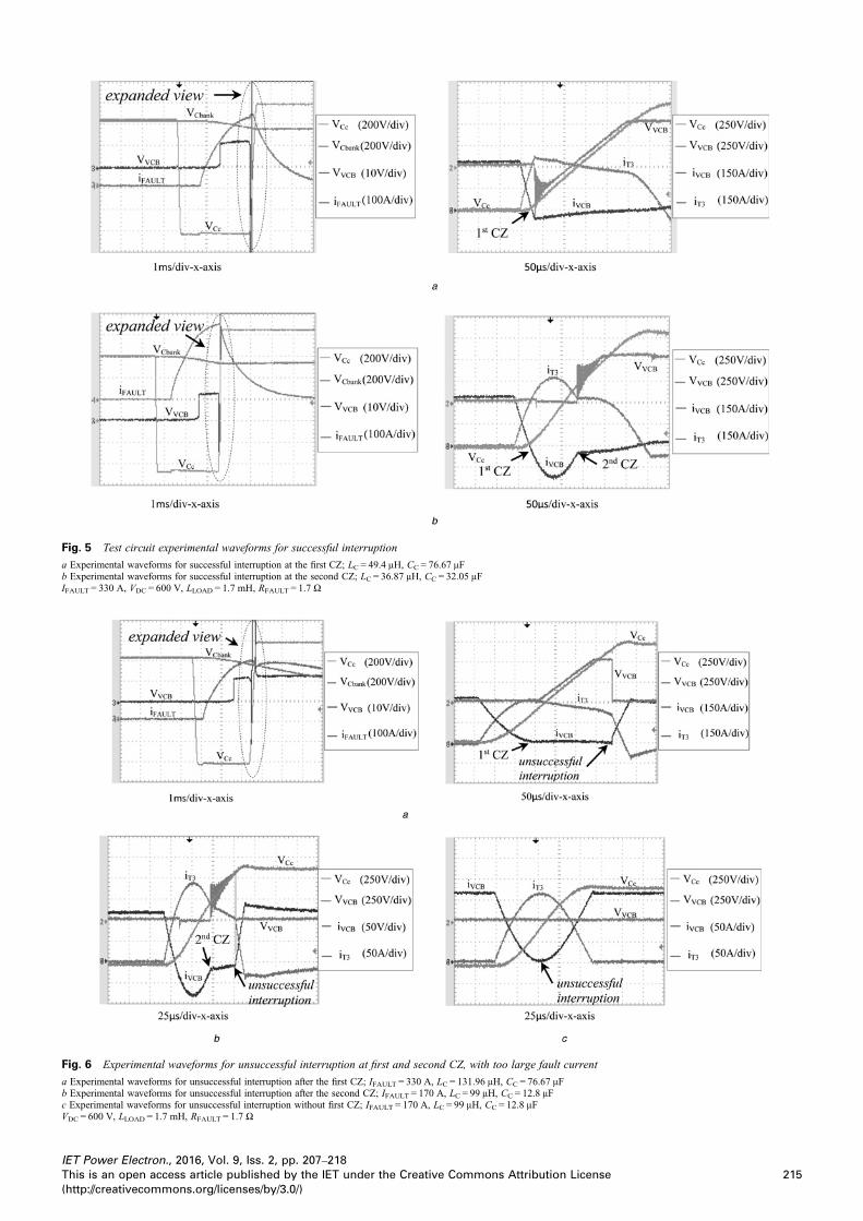
Fig. 5 Test circuit experimental waveforms for successful interruption
a Experimental waveforms for successful interruption at the first CZ; LC = 49.4 μH, CC = 76.67 μFb Experimental waveforms for successful interruption at the second CZ; LC = 36.87 μH, CC = 32.05 μFIFAULT = 330 A, VDC = 600 V, LLOAD = 1.7 mH, RFAULT = 1.7 Ω
Fig. 6 Experimental waveforms for unsuccessful interruption at first and second CZ, with too large fault current
a Experimental waveforms for unsuccessful interruption after the first CZ; IFAULT = 330 A, LC = 131.96 μH, CC = 76.67 μFb Experimental waveforms for unsuccessful interruption after the second CZ; IFAULT = 170 A, LC = 99 μH, CC = 12.8 μFc Experimental waveforms for unsuccessful interruption without first CZ; IFAULT = 170 A, LC = 99 μH, CC = 12.8 μFVDC = 600 V, LLOAD = 1.7 mH, RFAULT = 1.7 Ω
IET Power Electron., 2016, Vol. 9, Iss. 2, pp. 207–218215This is an open access article published by the IET under the Creative Commons Attribution License
(http://creativecommons.org/licenses/by/3.0/)

Fig. 7 Experimental waveforms for successful interruptions with same interrupting current but different gap distance
a Gap distance 1 mmb Gap distance 2 mmIFAULT = 330 A, VDC = 600 V, LC = 36.87 μH, CC = 32.05 μF, LLOAD = 1.7 mH, RFAULT = 1.7 Ω
Fig. 8 VCB interruption characteristics
a Relationship between di/dt and dVVCB/dt with 1 mm gap distance; IFAULT = 90 and 330 Ab Relationship between di/dt and dVVCB/dt with 1 and 2 mm gap distance; IFAULT = 90 Ac Relationship between varied interruption current, di/dt and arcing time with 1 mm gap distance; IFAULT = 110, 170, 220 and 330 Ad Relationship between varied interruption current, di/dt and arcing time with 1 mm gap distance; IFAULT = 90 A
IET Power Electron., 2016, Vol. 9, Iss. 2, pp. 207–218216 This is an open access article published by the IET under the Creative Commons Attribution License
(http://creativecommons.org/licenses/by/3.0/)
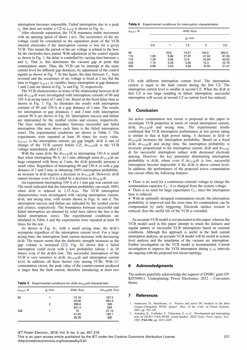
Table 4 Experimental conditions for interruption characteristics
iFAULT, A di/dt, A/μs
g, mm
0.5 1 1.5 2 2.5
90 – 20.5 73.27 150.5 302.5110 1.69 5.86 21.97 47.62 61.34170 1.29 3.85 12.5 24.93 42.03220 1.19 3.29 5.05 12.3 22.78330 0.89 2.53 4.08 15.55 21.41
interruption becomes impossible. Failed interruption due to a peakiT3 that does not realise a CZ in iVCB is shown in Fig. 6c.
After electrode separation, the VCB maintains stable movementwith an opening speed of about 1 m/s. The occurrence of the arcvoltage could be considered as the separation point of the VCBinternal electrodes if the interruption current is low for a givenVCB. This means the period of the arc voltage is related to the howfar the electrodes have parted. With adjustment of the control signalsas shown in Fig. 1, the delay is controlled by varying time between t1and t2. That is, this determines the vacuum gap at point thatcommutation starts. Thus, the VCB can be interrupt at the samecurrent level for different gap distances, by adjustment of the controlsignals as shown in Fig. 7. In this figure, the time between VCc
beenreversed and the occurrence of arc voltage is fixed at 2 ms, but thetime to trigger iFAULT is variable; hence interruption at gap distances1 and 2 mm are shown in Fig. 7a and Fig. 7b, respectively.
The VCB characteristics in terms of the relationship between di/dtand dvVCB/dt were investigated with interruption currents of 90 and330 A at arcing times of 1 and 2 ms. Based on the fixed delay time asshown in Fig. 7, Fig. 8a illustrates the results with interruptioncurrents of 90 and 330 A at a gap distance of 1 mm. The resultsfor interruption at gap distances 1 and 2 mm with interruptioncurrent 90 A are shown in Fig. 8b. Interruption success and failureare represented by the symbol circles and crosses, respectively.The lines indicate the boundary between successful and failedinterruption (the area above each lines is the failed interruptionzone). The experimental conditions are shown in Table 3. Theexperiments were repeated at least 30 times for every value.iFAULT is the interruption current; gis gap length; di/dt is rate ofchange of the VCB current before CZ; dvVCB/dt is the VCBvoltage immediately after CZ.
With the same di/dt, the dvVCB/dt in interrupting 330 A is smallthan when interrupting 90 A. At 1 mm, although some dvVCB/dt arelarge compared with those at 2 mm, the di/dt generally presents asmall value. Regardless of interrupting 90 and 330 A or with a gapdistance of 1 and 2 mm, in obtaining 100% interruption probability,an increase in di/dt requires a decrease in dvVCB/dt. However, di/dtcannot increase even if it is aided by a decrease in dvVCB/dt.
An experiment interrupting 330 A at a 1 mm gap was carried out.The result indicated that the interruption probability can reach 100%when di/dt is reduced to 2.53 A/μs. The VCB interruptioncharacteristics were investigated with varying interruption current,di/dt, and arcing time, with results shown in Figs. 8c and d. Theinterruption success and failure are indicated by the symbol circlesand crosses, respectively. The boundaries between successful andfailed interruption are denoted by solid lines (above the line is thefailed interruption zone). The experimental conditions aretabulated in Table 4 and the experiments were repeated at least 30times for the test.
As shown in Fig. 8c, with a small arcing time, the di/dt′sasymptote regardless of the interruption current level. For a largearcing time, the interruption limit current increases with decreasingdi/dt. The reason seems that the dielectric strength increases as thegap volume is increased [22]. Fig. 8d shows that a failedinterruption could occur with a low probability (about 1 in 30times) even if the di/dtis low. The successful interruption of theVCB is very sensitive to di/dt, dvVCB/dt and interruption currentlevel. In addition, all these factors vary among VCBs. With LCcommutation circuit, the peak value of the counter-current producedis larger than the fault current, therefore introducing at most two
Table 3 Experimental conditions for di/dt–dvVCB/dt characteristic
iFAULT, A g, mm di/dt, A/μs dvVCB/dt, V/μs
90 1 73.18 187.540.68 692.3
2 398.6 300201.4 500
330 1 70 47.1441.92 194.136.39 300
IET Power Electron., 2016, Vol. 9, Iss. 2, pp. 207–218This is an open access article published by the IET under the Creative(http://creativecommons.org/licenses/by/3.0/)
CZs with different interruption current level. The interruptioncurrent is equal to the fault current during the first CZ. Theinterruption current level is smaller at second CZ. When the di/dt atfirst CZ is too large resulting in failure interruption, successfulinterruption will occurs at second CZ as current level has reduced.
5 Conclusion
An active commutation test circuit is proposed in this paper toinvestigate VCB properties in terms of varied interruption current,di/dt, dvVCB/dt and arcing time. The experimental resultsconfirmed that VCB interruption performance at low power ratingis similar to that at high power rating. A decrease in di/dt ordvVCB/dt increases the interruption probability. Based on a fixeddi/dt, dvVCB/dt and arcing time, the interruption probability isinversely proportional to the interruption current. di/dt and dvVCB/dt for successful interruption reduce with decreased electrodespacing. However, the key parameter determining interruptionprobability is di/dt, where even if dvVCB/dt is low, successfulinterruption become impossible if the di/dt is above certain level.In addition, the performance of the proposed active commutationtest circuit offers the following features:
† There is no need for a continuous external voltage to charge thecommutation capacitor CC: it is charged from the system voltage.† There is no need for large capacitance CC, since the interruptiontime is reduced.† With an optimally designed commutation circuit, the interruptionprobability is improved and the extra time for commutation can becompensated by early triggering. Electrode surface erosion isreduced, thus the useful life of the VCB is extended.
An accurate VCB model is not presented in this paper, whereas theVCB model used in this paper attempt to retain the features andregular pattern of successful VCB interruptions based on externalconditions. Although this approach is useful in the fault currentinterruption analysis, an accurate VCB model will be useful in systemlevel analysis and the simulation of the vacuum arc interruption.Further investigation on the VCB model is recommended. Currentinvestigation to improve the VCB interruption during t2–t6 intervalsare ongoing with the proposed test circuit topology.
6 Acknowledgments
The authors gratefully acknowledge the support of EPSRC grant EP/K035096/1: Underpinning Power Electronics 2012 - Converterstheme.
7 References
1 Andersson, D., Henriksson, A.: ‘Passive and active DC breakers in the threeGorges–Changzhou HVDC project’. Proc. of Int. Conf. on Power Systems,2001, pp. 391–395
2 Arimatsu, K., Yoshioka, Y., Tokuyama, S., et al.: ‘Development and interruptingtests on 250 KV 8 KA HVDC circuit breaker’, IEEE Trans. Power Appar. Syst.,1985, PAS-104, pp. 2452–2459
217Commons Attribution License
3 Pauli, B., Ruoss, E., Mauthe, G., et al.: ‘Development of a high current HVDCcircuit breaker with fast fault clearing capability’, IEEE Trans. Power Deliv.,1988, 3, pp. 2072–2080
4 Pucher, W.: ‘Fundamentals of HVDC interruption’, Electra, 1968, ELT_005_1pp. 24–38
5 Premerlani, W.J.: ‘Forced commutation performance of vacuum switches forHVDC breaker application’, IEEE Trans., 1982, PAS-101, pp. 2721–2727
6 Kontos, E., Teixeira, R., Rodrigues, S., et al.: ‘Impact of HVDC transmissionsystem topology on multi-terminal DC network faults’, IEEE Trans. PowerDeliv., 2015, 30, (2), pp. 844–852
7 Sneath, J., Rajapakse, A.: ‘Fault detection and interruption in an earthed HVDCgrid using ROCOV and hybrid DC breakers’, IEEE Trans. Power Deliv., doi:10.1109/TPWRD.2014.2364547, IEEE Early Access Articles, 2014, 99, p. 1
8 Derakhshanfar, R., Jonsson, T., Steiger, U., et al.: ‘Hybrid HVDC breaker-asolution for future HVDC system’ (CIGRE, 2014)
9 Hassanpoor, A., Hafner, J., Jacobson, B.: ‘Technical assessment of loadcommutation switch in hybrid HVDC breaker’, IEEE Trans. Power Electron.,doi:10.1109/TPEL.2014.2372815, 2015, 30, pp. 5393–5400
10 ABB: ‘The hybrid HVDC breaker an innovation breakthrough enabling reliableHVDC grids’. Available at http://www05.abb.com/global/scot/scot221.nsf/veritydisplay/c9d5ba256e7e9671c1257ab6004b1feb/$file/hybrid-hvdc-breaker-an-innovation-breakthrough-for-reliable-hvdc-gridsnov2012.pdf
11 ABB: ‘PatentUS2013/0070492’,HighVoltageDCBreakerApparatus, 21March201312 Eriksson, T., Backman, M., Halen, S.: ‘A low loss mechanical HVDC breaker for
HVDC grid applications’ (CIGRE, Paris, 2014)
218 This is an open access article publi
13 Tahata, K., Ka, S., Tokoyoda, S., et al.: ‘HVDC circuit breakers for HVDC gridapplications’. AORC Technical Meeting, 2014, pp. 1–8
14 Tahata, K., El Outkaili, S., Kamei, K., et al.: ‘HVDC circuit breakers for HVDCgrid applications’. IET ACDC 2015 Conf., 2015
15 Franck, C.M.: ‘HVDC circuit breakers: a review identifying future research needs’,IEEE Trans. Power Deliv., 2011, 26, pp. 998–1007
16 Odaka, H., Yamada, M., Sakuma, R., et al.: ‘DC interruption characteristic ofvacuum circuit breaker’, Electr. Eng. Jpn, 2007, 161, pp. 17–25
17 Niwa, Y., Matsuzaki, J., Yokokura, K.: ‘The basic investigation of the high-speedVCB and its application for the DC power system’. 23rd Int. Symp. on Dischargesand Electrical Insulation in Vacuum, 2008, ISDEIV 2008, 2008, vol. 1,pp. 107–112
18 Niwa, Y., Funahashi, T., Yokokura, K., et al.: ‘Basic investigation of a high-speedvacuum circuit breaker and its vacuum arc characteristics’, IEE Proc., Gener.Transm. Distrib., 2006, 153, pp. 11–15
19 Greenwood, A.N., Lee, T.H.: ‘Theory and application of the commutation principlefor HVDC circuit breakers’, IEEE Trans. Power Appar. Syst. 1972, PAS-91,pp. 1570–1574
20 Greenwood, A.N., Barkan, P., Kracht, W.C.: ‘HVDC vacuum circuit breakers’,IEEE Trans. Power Appar. Syst., 1972, PAS-91, pp. 1575–1588
21 Wallacetown, A.: ‘Vacuum contactors’, August 2008, pp. 1–622 van Lanen, E., Smeets, R., Popov, M., et al.: ‘Vacuum circuit breaker postarc
current modelling based on the theory of Langmuir probes’, IEEE Trans.Plasma Sci., 2007, 35, pp. 925–932
IET Power Electron., 2016, Vol. 9, Iss. 2, pp. 207–218shed by the IET under the Creative Commons Attribution License
(http://creativecommons.org/licenses/by/3.0/)