gcd: vlsi's hello world overview
TRANSCRIPT
GCD: VLSI’s Hello World
EE241 TutorialWritten by Yunsup Lee (2010)
Updated by Brian Zimmer (2011,2013)
Overview
For this tutorial, you will become familiar with the VLSI tools you will use throughout this semesterand learn how a design “flows” through the toolflow. Specifically, given an RTL model of a simplegreatest common divisor (GCD) circuit, you will synthesize and place and route the design, simulateat every stage, and analyze power.
VLSI Toolflow Introduction
Figure 1 shows the toolflow you will be using for the first lab. You will use Synopsys VCS (vcs)to simulate and debug your RTL design. After you get your design right, you will use SynopsysDesign Compiler (dc shell-xg-t) to synthesize the design. Synthesis is the process of transformingan RTL model into a gate-level netlist. VCS is used again to simulate the synthesized gate-levelnetlist. After obtaining a working gate-level netlist, you will use Synopsys IC Compiler (icc shell)to place and route the design. Placement is the process by which each standard cell is positioned onthe chip, while routing involves wiring the cells together using various metal layers. The tools willprovide feedback on the performance and area of your design after both synthesis and place androute. The results from place and route are more realistic but require much more time to generate.After place and route, you will generate and simulate the final gate-level netlist using VCS. Finallyyou will use this gate-level simulation as a final test for correctness and to generate transition countsfor every net in the design. Synopsys PrimeTime PX (pt shell) takes these transition counts asinput and correlate them with the capacitance values in the final layout to produce estimated powermeasurements. The diagram below shows how every tools works together.
Prerequisites
As you can easy tell from the diagram, many different tools are needed to take even a simple designfrom RTL all the way to transistor-level implementation. Each tool is immensely complicated, andmany engineers in industry specialize in only one. In order to produce a VLSI design in a singlesemester we will need to understand a little about every one.
Each tool has a GUI interface. However, most inputs that the tools need are the same for everydesign iteration and become repetitive to type, so .tcl scripts provide all of the inputs needed. Whenyou use the GUI, in the terminal window you will see the textual equivalent of each click, and thesecommands can be added to scripts. To keep files organized, each piece of the toolflow has its ownbuild directory and its own Makefile. The Makefile initializes the program and points at the setupscripts. A top-level Makefile runs each program in succession so that ideally, a single command willpush an RTL design all of the way through the flow without any repetitive intervention.

EE241 Tutorial, GCD: VLSI’s Hello World, Spring 2013 2
VerilogSource(RTL)
VCS Design Compiler
IC Compiler (DP)
IC Compiler (P&R)
ConstraintsFile
Constraints
Std.Cell
Library
RTLSim Results
GateLevelNetlist
TimingArea
DelayFile
TLU+Files
FloorPlan
ConstraintsFile
GateLevelNetlist
TimingArea Layout Parasitics
FileDelayFile
VCS
PostSynSim
Results
VCS
Post P&RSim Results
PrimeTime
Switching activity
PowerEstimates
Figure 1: EE241 Toolflow for Lab 1
EE241 Tutorial, GCD: VLSI’s Hello World, Spring 2013 3
Getting Started
All of the EE241 laboratory assignments should be completed on an EECS Instructional machine.Please see the course website and follow all of the instructions for setting up your computingresources. Remember, you will need to source a setup script in order for these instructions to work.This bash script contains the location of each tool’s binary, and also sets up important environmentvariables. Make sure you have followed class setup instructions before starting (these are postedon the website).
As these tools generate enormous amounts of data and home directories have too low of a diskquota, we will need to use the local disk of one of the available. Assuming your username is userA(change this to your own username), you can create your personal git directory using the followingcommand.
% cd /scratch/
% mkdir userA
To begin the lab you will need to make use of a provided lab harness. This lab harness providesmakefiles, scripts, and the Verilog test harness required to complete the tutorial. The followingcommands grab these files from the class repository. To simplify the rest of the lab we will alsodefine a ’$LABROOT’ environment variable which contains the absolute path to the project’stop-level root directory.
% cd /scratch/userA
% git clone ~ee241/tutorials/gcd
% cd gcd
% LABROOT=$PWD
Every time you want to start the tools, you must source your environment variable.
% source ~ee241/tutorials/ee241.bashrc
Note: scratch/ is a local drive, so if you every need to do work on another machine, you will needto rsync files between machines.
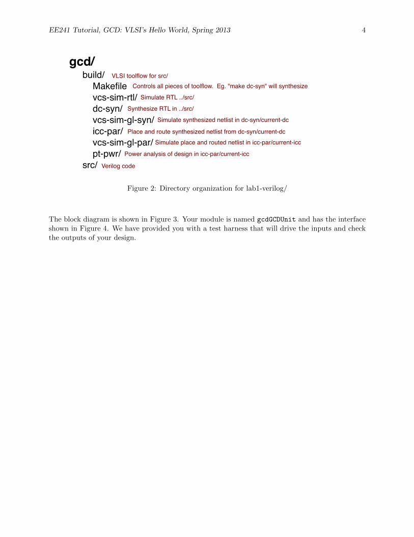
The resulting $LABROOT directory contains the following primary subdirectories: src contains yoursource Verilog; build contains automated makefiles and scripts for building your design. The src
directory contains the Verilog test harness and other Verilog modules you will need in this labassignment. Figure 2 shows each directory that you have been given and includes comments aboutwhat they do.
RTL:
• src/gcdGCDUnit rtl.v - RTL implementation of gcdGCDUnit
• src/gcdGCDUnitCtrl.v - Control part of the RTL implementation
• src/gcdGCDUnitDpath.v - Datapath part of the RTL implementation
• src/gcdTestHarness rtl.v - Test harness for the RTL model
EE241 Tutorial, GCD: VLSI’s Hello World, Spring 2013 4
build/ Makefile vcs-sim-rtl/ dc-syn/ vcs-sim-gl-syn/ icc-par/ vcs-sim-gl-par/ pt-pwr/ src/ Verilog code
VLSI toolflow for src/Controls all pieces of toolflow. Eg. "make dc-syn" will synthesize
Simulate RTL ../src/
Synthesize RTL in ../src/
Simulate synthesized netlist in dc-syn/current-dc
Place and route synthesized netlist from dc-syn/current-dcSimulate place and routed netlist in icc-par/current-icc
Power analysis of design in icc-par/current-icc
gcd/
Figure 2: Directory organization for lab1-verilog/
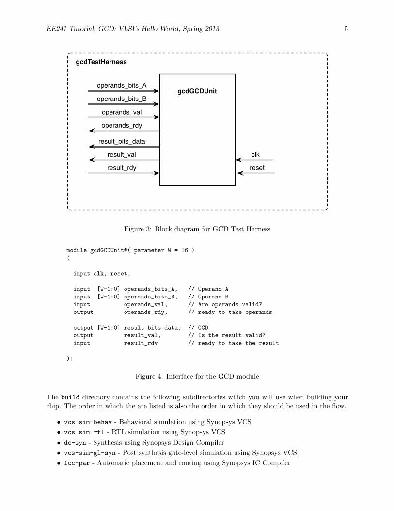
The block diagram is shown in Figure 3. Your module is named gcdGCDUnit and has the interfaceshown in Figure 4. We have provided you with a test harness that will drive the inputs and checkthe outputs of your design.
EE241 Tutorial, GCD: VLSI’s Hello World, Spring 2013 5
gcdGCDUnit
gcdTestHarness
operands_bits_A
operands_bits_B
operands_val
operands_rdy
result_bits_data
result_rdy
result_val clk
reset
Figure 3: Block diagram for GCD Test Harness
module gcdGCDUnit#( parameter W = 16 )
(
input clk, reset,
input [W-1:0] operands_bits_A, // Operand A
input [W-1:0] operands_bits_B, // Operand B
input operands_val, // Are operands valid?
output operands_rdy, // ready to take operands
output [W-1:0] result_bits_data, // GCD
output result_val, // Is the result valid?
input result_rdy // ready to take the result
);
Figure 4: Interface for the GCD module
The build directory contains the following subdirectories which you will use when building yourchip. The order in which the are listed is also the order in which they should be used in the flow.
• vcs-sim-behav - Behavioral simulation using Synopsys VCS
• vcs-sim-rtl - RTL simulation using Synopsys VCS
• dc-syn - Synthesis using Synopsys Design Compiler
• vcs-sim-gl-syn - Post synthesis gate-level simulation using Synopsys VCS
• icc-par - Automatic placement and routing using Synopsys IC Compiler
EE241 Tutorial, GCD: VLSI’s Hello World, Spring 2013 6
• vcs-sim-gl-par - Post place and route gate-level simulation using Synopsys VCS
• pt-pwr - Power analysis using Synopsys PrimeTime PX
Each subdirectory includes its own makefile and additional script files. So for example, to synthesizewith Design Compiler (DC):
% cd $LABROOT/build
% cd dc-syn
% make
Note: you must follow the ordering given in the list above.
Once you have all the tools working you can use the toplevel makefile in the build directory to runmultiple tools at once. For example, once all the scripts are properly setup you should be able touse the following command to synthesize, floorplan, and place and route your design. You give thecommand for the furthest step in the flow you would like to go to, and the Makefile’s dependenciesensures that every step before this step is completed first.
% cd $LABROOT/build
% make icc-par
Pushing the design through all the VLSI Tools
You will now go through the entire tool flow and inspect the results after each step.
Synopsys VCS: Simulating your Verilog
VCS compiles source Verilog into a cycle-accurate executable for simulation. VCS can compileVerilog expressed behaviorally, at the RTL level, or as structural verilog (a netlist). BehavioralVerilog cannot be synthesized and should only be used in testbenches. RTL-level Verilog expressesbehavior as combinational and sequential logic at a higher level. Structural-level Verilog expressesbehavior as specific gates wired together. You will start with simulating the GCD module RTL(before it is synthesized).
% cd $LABROOT/build/vcs-sim-rtl
% make
% make run
./simv +verbose=1
...
+ Running Test Case: gcdGCDUnit_rtl
[ passed ] Test ( vcTestSink ) succeeded, [ 0003 == 0003 ]
[ passed ] Test ( vcTestSink ) succeeded, [ 0007 == 0007 ]
[ passed ] Test ( vcTestSink ) succeeded, [ 0005 == 0005 ]
[ passed ] Test ( vcTestSink ) succeeded, [ 0001 == 0001 ]
[ passed ] Test ( vcTestSink ) succeeded, [ 0028 == 0028 ]
[ passed ] Test ( vcTestSink ) succeeded, [ 000a == 000a ]
[ passed ] Test ( vcTestSink ) succeeded, [ 0005 == 0005 ]
[ passed ] Test ( vcTestSink ) succeeded, [ 0000 == 0000 ]
EE241 Tutorial, GCD: VLSI’s Hello World, Spring 2013 7
[ passed ] Test ( Is sink finished? ) succeeded
...
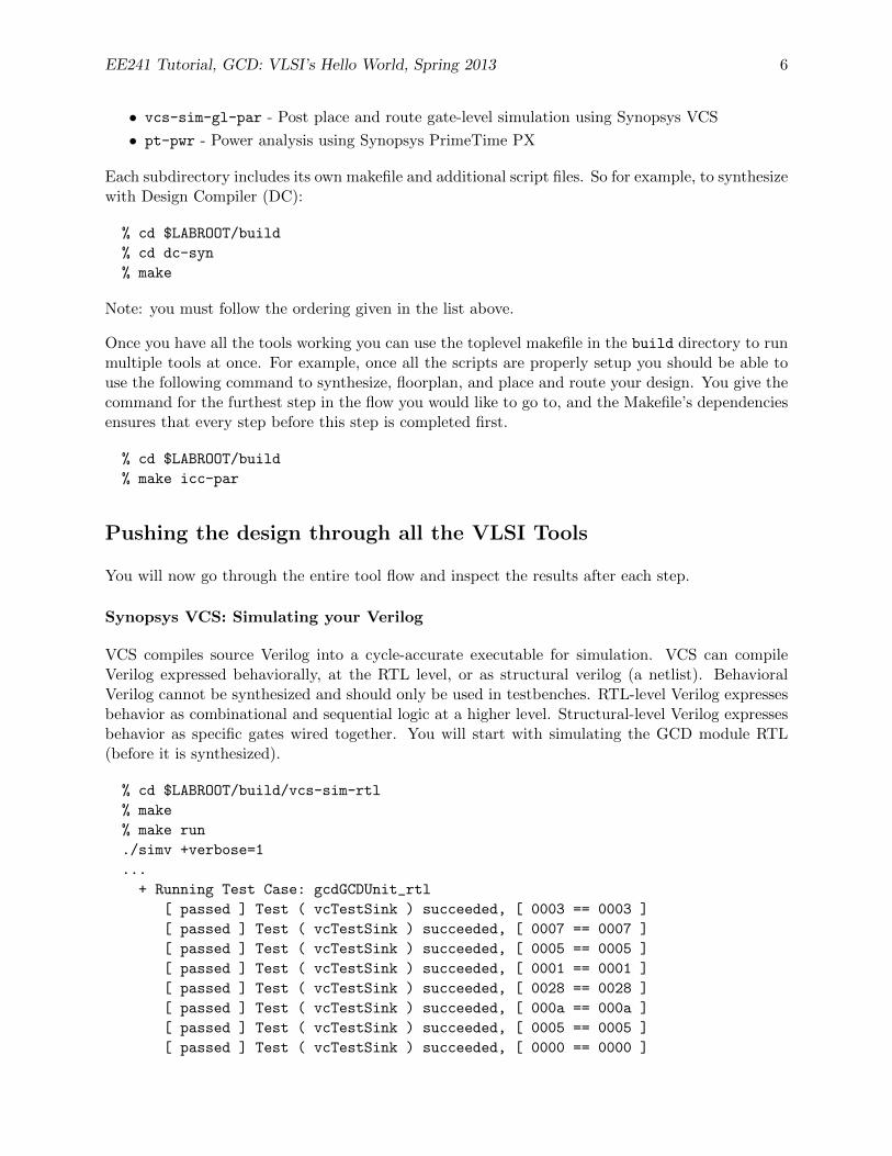
Where should you start if all of your tests didn’t pass? The answer is debug your RTL usingDiscovery Visualization Environment (DVE) GUI looking at the trace outputs. The simulatoralready logged the activity for every net to the vcdplus.vpd file. DVE can read the vcdplus.vpd
file and visualize the wave form.
% dve -vpd vcdplus.vpd &
To add signals to the waveform window (see Figure 5) you can select them in the hierarchy windowand then right click to choose Add To Waves > New Wave View.
Figure 5: DVE Waveform Window
Synopsys Design Compiler: RTL to Gate-Level Netlist
Design Compiler performs hardware synthesis. A synthesis tool takes an RTL hardware descriptionand a standard cell library as input and produces a gate-level netlist as an output. The resultinggate-level netlist is a completely structural description with only standard cells at the leaves of thedesign.
% cd $LABROOT/build/dc-syn
% make
Go ahead and take a look what the automated build system produced.
% cd $LABROOT/build/dc-syn
% ls -l
-rw-r--r-- 1 yunsup grad 4555 Aug 29 22:15 Makefile
drwxr-xr-x 7 yunsup grad 4096 Aug 29 22:15 build-dc-2010-08-29_22-15
-rw-r--r-- 1 yunsup grad 1108 Aug 28 12:06 constraints.tcl
EE241 Tutorial, GCD: VLSI’s Hello World, Spring 2013 8
lrwxrwxrwx 1 yunsup grad 25 Aug 29 22:15 current-dc -> build-dc-2010-08-29_22-15
drwxr-xr-x 2 yunsup grad 4096 Aug 29 21:39 rm_dc_scripts
drwxr-xr-x 2 yunsup grad 4096 Aug 28 12:00 rm_notes
drwxr-xr-x 2 yunsup grad 4096 Aug 29 21:50 rm_setup
% cd current-dc
% ls -l
drwxr-xr-x 2 yunsup grad 4096 Aug 29 22:15 WORK
-rw-r--r-- 1 yunsup grad 47 Aug 29 22:15 access.tab
-rw-r--r-- 1 yunsup grad 235827 Aug 29 22:15 command.log
-rw-r--r-- 1 yunsup grad 5141 Aug 29 22:15 common_setup.tcl
-rw-r--r-- 1 yunsup grad 1108 Aug 29 22:15 constraints.tcl
-rw-r--r-- 1 yunsup grad 18996 Aug 29 22:15 dc.tcl
-rw-r--r-- 1 yunsup grad 4621 Aug 29 22:15 dc_setup.tcl
-rw-r--r-- 1 yunsup grad 4625 Aug 29 22:15 dc_setup_filenames.tcl
-rw-r--r-- 1 yunsup grad 2730 Aug 29 22:15 find_regs.tcl
-rw-r--r-- 1 yunsup grad 4439 Aug 29 22:15 force_regs.ucli
drwxr-xr-x 3 yunsup grad 4096 Aug 29 22:15 gcdGCDUnit_rtl_LIB
drwxr-xr-x 2 yunsup grad 4096 Aug 29 22:15 log
-rw-r--r-- 1 yunsup grad 1087 Aug 29 22:15 make_generated_vars.tcl
drwxr-xr-x 2 yunsup grad 4096 Aug 29 22:15 reports
drwxr-xr-x 2 yunsup grad 4096 Aug 29 22:15 results
-rw-r--r-- 1 yunsup grad 29 Aug 29 22:15 timestamp
Notice that the makefile does not overwrite build directories. It always create new build directories.This makes it easy to change your synthesis scripts or source Verilog, resynthesize your design, andcompare your results to previous designs. You can use symlinks to keep track of various builddirectories. Inside the current-dc directory, you can see all the tcl scripts as well as the directoriesnamed results and reports: results contains your synthesized gate-level netlist; and reports
contains various post synthesis reports.
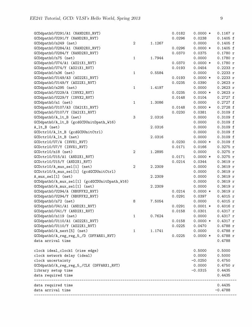
Take a look at various reports on synthesis results.
% cd $LABROOT/build/dc-syn/current-dc/reports
% cat gcdGCDUnit_rtl.mapped.timing.rpt
Startpoint: GCDdpath0/B_reg_reg_11_
(rising edge-triggered flip-flop clocked by ideal_clock1)
Endpoint: GCDdpath0/A_reg_reg_5_
(rising edge-triggered flip-flop clocked by ideal_clock1)
Path Group: ideal_clock1
Path Type: max
Point Fanout Cap Trans Incr Path
----------------------------------------------------------------------------------------------
clock ideal_clock1 (rise edge) 0.0000 0.0000
clock network delay (ideal) 0.0000 0.0000
GCDdpath0/B_reg_reg_11_/CLK (DFFARX1_RVT) 0.0000 0.0000 0.0000 r
GCDdpath0/B_reg_reg_11_/Q (DFFARX1_RVT) 0.0269 0.0999 0.0999 f
GCDdpath0/B_reg[11] (net) 2 2.4320 0.0000 0.0999 f
GCDdpath0/U77/A (INVX2_RVT) 0.0269 0.0000 * 0.0999 f
GCDdpath0/U77/Y (INVX2_RVT) 0.0182 0.0167 0.1166 r
GCDdpath0/n38 (net) 3 2.4349 0.0000 0.1166 r
EE241 Tutorial, GCD: VLSI’s Hello World, Spring 2013 9
GCDdpath0/U291/A1 (NAND2X0_RVT) 0.0182 0.0000 * 0.1167 r
GCDdpath0/U291/Y (NAND2X0_RVT) 0.0296 0.0238 0.1405 f
GCDdpath0/n249 (net) 2 1.1267 0.0000 0.1405 f
GCDdpath0/U284/A1 (NAND2X0_RVT) 0.0296 0.0000 * 0.1405 f
GCDdpath0/U284/Y (NAND2X0_RVT) 0.0370 0.0375 0.1780 r
GCDdpath0/n75 (net) 1 1.7944 0.0000 0.1780 r
GCDdpath0/U74/A1 (AO21X1_RVT) 0.0370 0.0000 * 0.1780 r
GCDdpath0/U74/Y (AO21X1_RVT) 0.0193 0.0454 0.2233 r
GCDdpath0/n36 (net) 1 0.5584 0.0000 0.2233 r
GCDdpath0/U149/A3 (AO22X1_RVT) 0.0193 0.0000 * 0.2233 r
GCDdpath0/U149/Y (AO22X1_RVT) 0.0235 0.0390 0.2623 r
GCDdpath0/n295 (net) 1 1.4197 0.0000 0.2623 r
GCDdpath0/U229/A (INVX2_RVT) 0.0235 0.0000 * 0.2623 r
GCDdpath0/U229/Y (INVX2_RVT) 0.0148 0.0104 0.2727 f
GCDdpath0/n1 (net) 1 1.3086 0.0000 0.2727 f
GCDdpath0/U107/A3 (OA21X1_RVT) 0.0148 0.0000 * 0.2728 f
GCDdpath0/U107/Y (OA21X1_RVT) 0.0230 0.0381 0.3109 f
GCDdpath0/A_lt_B (net) 3 2.0316 0.0000 0.3109 f
GCDdpath0/A_lt_B (gcdGCDUnitDpath_W16) 0.0000 0.3109 f
A_lt_B (net) 2.0316 0.0000 0.3109 f
GCDctrl0/A_lt_B (gcdGCDUnitCtrl) 0.0000 0.3109 f
GCDctrl0/A_lt_B (net) 2.0316 0.0000 0.3109 f
GCDctrl0/U7/A (INVX1_RVT) 0.0230 0.0000 * 0.3109 f
GCDctrl0/U7/Y (INVX1_RVT) 0.0171 0.0166 0.3275 r
GCDctrl0/n18 (net) 2 1.2895 0.0000 0.3275 r
GCDctrl0/U15/A1 (AND2X1_RVT) 0.0171 0.0000 * 0.3275 r
GCDctrl0/U15/Y (AND2X1_RVT) 0.0214 0.0344 0.3619 r
GCDctrl0/A_mux_sel[1] (net) 2 2.2309 0.0000 0.3619 r
GCDctrl0/A_mux_sel[1] (gcdGCDUnitCtrl) 0.0000 0.3619 r
A_mux_sel[1] (net) 2.2309 0.0000 0.3619 r
GCDdpath0/A_mux_sel[1] (gcdGCDUnitDpath_W16) 0.0000 0.3619 r
GCDdpath0/A_mux_sel[1] (net) 2.2309 0.0000 0.3619 r
GCDdpath0/U294/A (NBUFFX2_RVT) 0.0214 0.0000 * 0.3619 r
GCDdpath0/U294/Y (NBUFFX2_RVT) 0.0291 0.0397 0.4015 r
GCDdpath0/n72 (net) 8 7.5054 0.0000 0.4015 r
GCDdpath0/U41/A1 (AND2X1_RVT) 0.0291 0.0001 * 0.4016 r
GCDdpath0/U41/Y (AND2X1_RVT) 0.0158 0.0301 0.4317 r
GCDdpath0/n119 (net) 1 0.7624 0.0000 0.4317 r
GCDdpath0/U110/A1 (AO22X1_RVT) 0.0158 0.0000 * 0.4317 r
GCDdpath0/U110/Y (AO22X1_RVT) 0.0225 0.0470 0.4788 r
GCDdpath0/A_next[5] (net) 1 1.1741 0.0000 0.4788 r
GCDdpath0/A_reg_reg_5_/D (DFFARX1_RVT) 0.0225 0.0000 * 0.4788 r
data arrival time 0.4788
clock ideal_clock1 (rise edge) 0.5000 0.5000
clock network delay (ideal) 0.0000 0.5000
clock uncertainty -0.0250 0.4750
GCDdpath0/A_reg_reg_5_/CLK (DFFARX1_RVT) 0.0000 0.4750 r
library setup time -0.0315 0.4435
data required time 0.4435
----------------------------------------------------------------------------------------------
data required time 0.4435
data arrival time -0.4788
----------------------------------------------------------------------------------------------
EE241 Tutorial, GCD: VLSI’s Hello World, Spring 2013 10
slack (VIOLATED) -0.0353
...
This report lists the critical path of the design. The critical path is the slowest logic between anytwo registers and is therefore the limiting factor preventing you from decreasing the clock periodconstraint. You can see that the critical path starts at bit 11 of the operand B register in thedatapath; goes through the comparator; to the control logic; and finally ends bit 5 of operand Aregister in the datapath. The critical path takes a total of 0.4788ns which is less than the 0.5nsclock period constraint.
If any of your paths say (VIOLATED) instead of (MET), you need to modify the build/Makefrag
file to increase the clock period. If you do not do this, your design will not pass simulation.
% vim $LABROOT/build/Makefrag
...
clock_period = 0.7
...
% cd $LABROOT/build/dc-syn/current-dc/reports
% cat gcdGCDUnit_rtl.mapped.area.rpt
...
Global cell area Local cell area
------------------ ---------------------------
Hierarchical cell Absolute Percent Combi- Noncombi- Black
Total Total national national boxes
-------------------------------- --------- ------- -------- --------- ------
gcdGCDUnit_rtl 966.5096 100.0 11.6906 0.0000 0.0000
GCDctrl0 56.4200 5.8 43.2045 13.2155 0.0000
GCDdpath0 898.3991 93.0 658.4871 228.2213 0.0000
GCDdpath0/clk_gate_A_reg_reg 5.8453 0.6 0.0000 5.8453 0.0000
GCDdpath0/clk_gate_B_reg_reg 5.8453 0.6 0.0000 5.8453 0.0000
-------------------------------- --------- ------- -------- --------- ------
Total 713.3822 253.1274 0.0000
...
This report tells you the post synthesis area results. The units are um2. You can see that thedatapath consumes 93.3% of the total chip area.
% cd $LABROOT/build/dc-syn/current-dc/reports
% cat gcdGCDUnit_rtl.mapped.power.rpt
...
--------------------------------------------------------------------------------
Switch Int Leak Total
Hierarchy Power Power Power Power %
--------------------------------------------------------------------------------
gcdGCDUnit_rtl 167.522 467.149 1.25e+08 760.139 100.0
GCDctrl0 (gcdGCDUnitCtrl) 5.927 35.039 6.75e+06 47.713 6.3
GCDdpath0 (gcdGCDUnitDpath_W16) 154.322 427.257 1.13e+08 695.001 91.4
...
EE241 Tutorial, GCD: VLSI’s Hello World, Spring 2013 11
This report tells you about post synthesis power results. The dynamic power units are uW whilethe leakage power units are pW .
% cd $LABROOT/build/dc-syn/current-dc/reports
% cat gcdGCDUnit_rtl.mapped.reference.rpt
...
****************************************
Design: gcdGCDUnitCtrl
****************************************
Reference Library Unit Area Count Total Area Attributes
-----------------------------------------------------------------------------
AND2X1_RVT saed32rvt_tt1p05v25c 2.033152 3 6.099456
AND2X2_RVT saed32rvt_tt1p05v25c 2.287296 3 6.861888
DFFX1_RVT saed32rvt_tt1p05v25c 6.607744 2 13.215488 n
INVX1_RVT saed32rvt_tt1p05v25c 1.270720 3 3.812160
NAND2X0_RVT saed32rvt_tt1p05v25c 1.524864 1 1.524864
NAND3X0_RVT saed32rvt_tt1p05v25c 1.779008 1 1.779008
NAND4X0_RVT saed32rvt_tt1p05v25c 2.033152 1 2.033152
NBUFFX2_RVT saed32rvt_tt1p05v25c 2.033152 1 2.033152
NOR2X0_RVT saed32rvt_tt1p05v25c 2.541440 3 7.624320
OA22X2_RVT saed32rvt_tt1p05v25c 2.795584 1 2.795584
OR2X1_RVT saed32rvt_tt1p05v25c 2.033152 2 4.066304
OR2X2_RVT saed32rvt_tt1p05v25c 2.287296 2 4.574592
-----------------------------------------------------------------------------
Total 12 references 56.419969
...
This report lists the standard cells used in each module.
% cd $LABROOT/build/dc-syn/current-dc/reports
% cat gcdGCDUnit_rtl.mapped.resources.rpt
...
===============================================================================
| | | Current | Set |
| Cell | Module | Implementation | Implementation |
===============================================================================
| sub_x_2 | DW01_sub | pparch (area,speed) |
| lt_x_3 | DW_cmp | apparch (area) | |
===============================================================================
...
Synopsys provides a library of commonly used arithmetic components as highly optimized buildingblocks. This library is called Design Ware and Design Compiler will automatically use DesignWare components when it can. This report can help you determine when Design Compiler is usingDesign Ware components. The DW01 sub in the module name indicates that this is a Design Waresubtractor. This report also gives you what type of architecutre it used.
Last, see what you actually created by viewing the post-synthesis netlist.
EE241 Tutorial, GCD: VLSI’s Hello World, Spring 2013 12
% cd $LABROOT/build/dc-syn/current-dc/results
% cat gcdGCDUnit_rtl.mapped.v
...
--------------------------------------------------------------------------------
Switch Int Leak Total
Hierarchy Power Power Power Power %
--------------------------------------------------------------------------------
gcdGCDUnit_rtl 167.522 467.149 1.25e+08 760.139 100.0
GCDctrl0 (gcdGCDUnitCtrl) 5.927 35.039 6.75e+06 47.713 6.3
GCDdpath0 (gcdGCDUnitDpath_W16) 154.322 427.257 1.13e+08 695.001 91.4
...
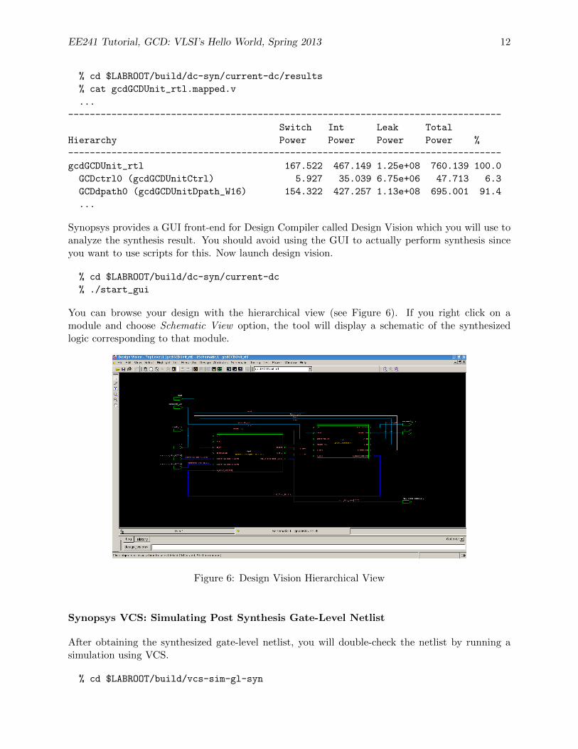
Synopsys provides a GUI front-end for Design Compiler called Design Vision which you will use toanalyze the synthesis result. You should avoid using the GUI to actually perform synthesis sinceyou want to use scripts for this. Now launch design vision.
% cd $LABROOT/build/dc-syn/current-dc
% ./start_gui
You can browse your design with the hierarchical view (see Figure 6). If you right click on amodule and choose Schematic View option, the tool will display a schematic of the synthesizedlogic corresponding to that module.
Figure 6: Design Vision Hierarchical View
Synopsys VCS: Simulating Post Synthesis Gate-Level Netlist
After obtaining the synthesized gate-level netlist, you will double-check the netlist by running asimulation using VCS.
% cd $LABROOT/build/vcs-sim-gl-syn
EE241 Tutorial, GCD: VLSI’s Hello World, Spring 2013 13
% make
% make run
...
+ Running Test Case: gcdGCDUnit_rtl
[ passed ] Test ( vcTestSink ) succeeded, [ 0003 == 0003 ]
[ passed ] Test ( vcTestSink ) succeeded, [ 0007 == 0007 ]
[ passed ] Test ( vcTestSink ) succeeded, [ 0005 == 0005 ]
[ passed ] Test ( vcTestSink ) succeeded, [ 0001 == 0001 ]
[ passed ] Test ( vcTestSink ) succeeded, [ 0028 == 0028 ]
[ passed ] Test ( vcTestSink ) succeeded, [ 000a == 000a ]
[ passed ] Test ( vcTestSink ) succeeded, [ 0005 == 0005 ]
[ passed ] Test ( vcTestSink ) succeeded, [ 0000 == 0000 ]
[ passed ] Test ( Is sink finished? ) succeeded
...
Synopsys IC Compiler: Gate-Level Netlist to Layout
IC Compiler performs place and route. This tool takes a synthesized gate-level netlist and astandard cell library as input and produces a layout as an output.
You can automate this process. Notice that the makefile creates new build directories like the onein Design Compiler.
% cd $LABROOT/build/icc-par
% make
% ls -l
-rw-r--r-- 1 yunsup grad 15232 Aug 28 18:40 Makefile
drwxr-xr-x 6 yunsup grad 4096 Aug 29 23:42 build-icc-2010-08-29_23-41
drwxr-xr-x 8 yunsup grad 4096 Aug 29 23:41 build-iccdp-2010-08-29_23-41
lrwxrwxrwx 1 yunsup grad 26 Aug 29 23:41 current-icc -> build-icc-2010-08-29_23-41
lrwxrwxrwx 1 yunsup grad 28 Aug 29 23:41 current-iccdp -> build-iccdp-2010-08-29_23-41
drwxr-xr-x 2 yunsup grad 4096 Aug 29 23:19 rm_icc_dp_scripts
drwxr-xr-x 2 yunsup grad 4096 Aug 29 23:29 rm_icc_scripts
drwxr-xr-x 2 yunsup grad 4096 Aug 29 23:38 rm_icc_zrt_scripts
drwxr-xr-x 2 yunsup grad 4096 Aug 28 16:20 rm_notes
drwxr-xr-x 2 yunsup grad 4096 Aug 29 23:34 rm_setup
After a few minutes, routing should have finished. Browse the results directory files to see similaroutputs as Design Compiler. Now open the GUI:
% cd $LABROOT/build/icc-syn/current-icc
% ./start_gui
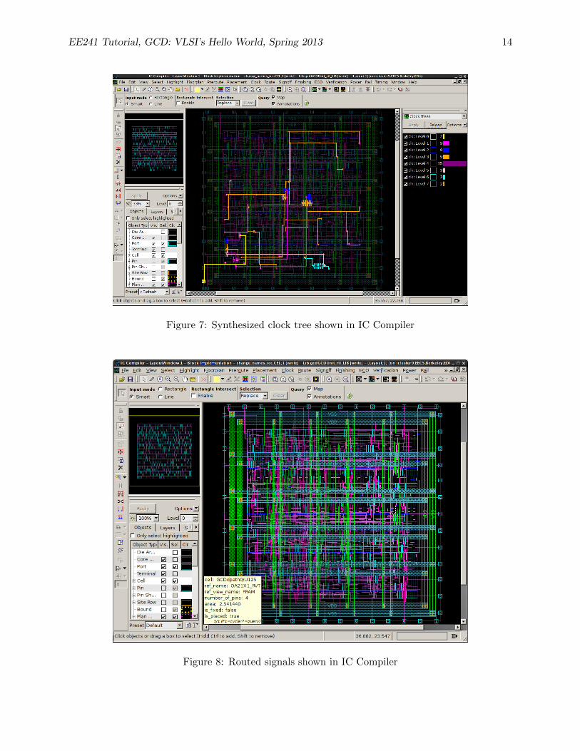
Take a look at the generated clock tree. Choose Clock > Color By Clock Trees. Hit Reload, and thenhit OK on the popup window. Now you will be able to see the synthesized clock tree (Figure 7).
Figure 8 shows the routed signals. Synopsys 32nm process provides nine metal layers (metal 1 ismostly used by the standard cell layout itself) to route your signals.
EE241 Tutorial, GCD: VLSI’s Hello World, Spring 2013 14
Figure 7: Synthesized clock tree shown in IC Compiler
Figure 8: Routed signals shown in IC Compiler

EE241 Tutorial, GCD: VLSI’s Hello World, Spring 2013 15
IC Compiler actual performs place and route in different steps. The Makefile runs then all at onceby default, but during default you can run only certain steps at a time. Go to File — Open Design,then try opening all of the different steps (for example: place opt icc), which shows ICC’s firstplacement.
The post place-and-route netlist can be found as current-icc/results/gcdGCDUnit rtl.output.v.
Synopsys VCS: Simulating Post Place and Route Gate-Level Netlist
After you obtain the post place and route gate-level netlist, you will double-check the netlist byrunning a simulation using VCS. You can use the makefile to build the post synthesis gate-levelnetlist simulator, run, and convert the switching activity file into a vcd and a saif format.
% cd $LABROOT/build/vcs-sim-gl-par
% make
% make run
% make convert
If your circuit no longer works (and it did after synthesis), this means that the added parasiticsfrom routing and clock tree issues increased your critical path. You can increase the clock periodfor the simulation testbench by editing Makefrag.
% vim $LABROOT/build/Makefrag
...
vcs_clock_period = 0$(shell echo "scale=4; ${clock_period}*0.5*1.2" | bc)
...
Synopsys PrimeTime PX: Estimating Power
PrimeTime PX is an add-on feature to PrimeTime that analyzes power dissipation of a cell-baseddesign. PrimeTime PX supports two types of power analysis modes. They are averaged mode andtime-based mode. Averaged mode calculates averaged power based on toggle rates. Time-basedmode let’s you know the peak power as well as the averaged power using gate-level simulationactivity.
% cd $LABROOT/build/pt-pwr
% make
Now look at some of the results
% cd $LABROOT/build/pt-pwr/current-pt/reports
% cat vcdplus.power.avg.max.report
...
Switch Int Leak Total
Hierarchy Power Power Power Power %
--------------------------------------------------------------------------------
gcdGCDUnit_rtl 3.84e-05 1.34e-04 1.57e-04 3.29e-04 100.0
GCDctrl0 (gcdGCDUnitCtrl) 2.60e-05 9.36e-05 1.24e-05 1.32e-04 40.2
GCDdpath0 (gcdGCDUnitDpath_W16) 1.22e-05 3.99e-05 1.41e-04 1.93e-04 58.8
EE241 Tutorial, GCD: VLSI’s Hello World, Spring 2013 16
% cat vcdplus.power.time.max.report
Switch Int Leak Peak Peak
Hierarchy Power Power Power Power Time
----------------------------------------------------------------------------------
gcdGCDUnit_rtl 3.84e-05 1.33e-04 1.57e-04 9.62e-03 49.331
GCDctrl0 (gcdGCDUnitCtrl) 2.60e-05 9.35e-05 1.24e-05 1.82e-03 43.914
GCDdpath0 (gcdGCDUnitDpath_W16) 1.22e-05 3.97e-05 1.41e-04 8.81e-03 49.331
Summary
You have now taken an RTL-level description in Verilog, then synthesized, place-and-routed, andanalyzed the power of the design. Each step is automated through Makefiles, and each step has itsown directory.
If you are interesting in learning more about how these scripts run, open the .log files in the directoryto see the commands that are run in each tool. Then open the tool directly (eg. type dc shell) andpaste in each line.
Acknowledgements
Many people have contributed to versions of this lab over the years. The lab was originally developedfor CS250 VLSI Systems Design course at University of California at Berkeley by Yunsup Lee.Contributors include: Krste Asanovic, Christopher Batten, John Lazzaro, and John Wawrzynek.Versions of this lab have been used in the following courses:
• CS250 VLSI Systems Design (2009-2010) - University of California at Berkeley
• CSE291 Manycore System Design (2009) - University of California at San Diego