gcd: vlsi’s hello worldcs250/fa10/handouts/lab1-gcd.pdf · gcd: vlsi’s hello world cs250...
TRANSCRIPT

GCD: VLSI’s Hello World
CS250 Laboratory 1 (Version 083010a)August 30, 2010Yunsup Lee
For the first lab assignment, you will write an RTL model of a greatest common divisor (GCD)circuit and push it through all the VLSI tools you will use in the class. The deliverables for this labare (a) your working Verilog RTL checked into a revision control system called Subversion (SVN),(b) build results and reports generated by VCS, DC Compiler, Formality, IC Compiler, PrimeTimePX checked into SVN, and (c) written answers to the questions given at the end of this document.The lab assignment is due at the start of class on Monday, September 13. You must submit yourwritten answers electronically by adding a directory titled writeup to your lab project directory(lab1/trunk/writeup). Electronic submissions must be in plain text or PDF format. You areencouraged to discuss your design with others in the class, but you must turn in your own work.
For this assignment, you will become familiar with the VLSI tools you will use this semester, learnhow a design “flows” through the toolflow, and practice Verilog coding.
Figure 1 shows the toolflow you will be using for the first lab. You will use Synopsys VCS (vcs) tosimulate and debug your RTL design. After you get your design right, you will use Synopsys DesignCompiler (dc shell-xg-t) to synthesize the design. Synthesis is the process of transforming anRTL model into a gate-level netlist. You will use Synopsys Formality (fm shell) to formally verifythat the RTL model and the gate-level model match. VCS is used again to simulate the synthesizedgate-level netlist. After obtaining a working gate-level netlist, you will use Synopsys IC Compiler(icc shell) to place and route the design. Placement is the process by which each standard cell ispositioned on the chip, while routing involves wiring the cells together using various metal layers.The tools will provide feedback on the performance and area of your design after both synthesisand place and route. The results from place and route are more realistic but require much moretime to generate. After place and route, you will generate and simulate the final gate-level netlistusing VCS. Finally you will use this gate-level simulation as a final test for correctness and togenerate transition counts for every net in the design. Synopsys PrimeTime PX (pt shell) takesthese transition counts as input and correlate them with the capacitance values in the final layoutto produce estimated power measurements.
Each piece of the toolflow has its own build directory and its own makefile. Please consult thefollowing tutorials for more information on using the various parts of the toolflow.
• Tutorial 2: Bits and Pieces of CS250’s Toolflow
• Tutorial 4: Simulating Verilog RTL using Synopsys VCS
• Tutorial 5: RTL-to-Gates Synthesis using Synopsys Design Compiler
• Tutorial 6: Automatic Placement and Routing using Synopsys IC Compiler
• Tutorial 7: Power Analysis using Synopsys PrimeTime PX

CS250 Lab Assignment 1 (Version 083010a), Fall 2010 2
Execute SIM
VerilogSource(Behav)
BehavSim
VCS
VPD TestOutputs
DVE GUI
VerilogSource(RTL)
VCS Design Compiler
Formality
Design Vision GUI
IC Compiler (DP)
IC Compiler (P&R)
ConstraintsFile
VerificationResults
ConstraintsStd.Cell
Library
RTLSim Gate
LevelNetlist
TimingArea
DelayFile
TLU+Files
FloorPlan
ConstraintsFile
GateLevelNetlist
TimingArea Layout Parasitics
FileDelayFile
Execute SIM
GuidanceFile
VPD TestOutputs
DVE GUI
VCS
PostSynSim
Execute SIM
VPD TestOutputs
DVE GUI
VCS
PostP&RSim
Execute SIM
VPD TestOutputs
DVE GUI
IC Compiler GUI
PrimeTime
VCD
VPD2VCD
PowerEstimates
Figure 1: CS250 Toolflow for Lab 1

CS250 Lab Assignment 1 (Version 083010a), Fall 2010 3
Block Diagram and Module Interface
The block diagram is shown in Figure 2. Your module should be named as gcdGCDUnit and musthave the interface shown in Figure 3. We have provided you with a test harness that will drive theinputs and check the outputs of your design.
gcdGCDUnit
gcdTestHarness
operands_bits_A
operands_bits_B
operands_val
operands_rdy
result_bits_data
result_rdy
result_val clk
reset
Figure 2: Block diagram for GCD Test Harness
module gcdGCDUnit#( parameter W = 16 )
(
input clk, reset,
input [W-1:0] operands_bits_A, // Operand A
input [W-1:0] operands_bits_B, // Operand B
input operands_val, // Are operands valid?
output operands_rdy, // ready to take operands
output [W-1:0] result_bits_data, // GCD
output result_val, // Is the result valid?
input result_rdy // ready to take the result
);
Figure 3: Interface for the GCD module

CS250 Lab Assignment 1 (Version 083010a), Fall 2010 4
Getting Started
You can follow along through the lab yourself by typing in the commands marked with a ’%’ symbolat the shell prompt. To cut and paste commands from this lab into your bash shell (and make surebash ignores the ’%’ character) just use an alias to ”undefine” the ’%’ character like this:
% alias %=""
All of the CS250 laboratory assignments should be completed on an EECS Instructional machine.Please see the course website for more information on the computing resources available for CS250students. Once you have logged into an EECS Instructional you will need to setup the CS250toolflow with the following commands.
% source ~cs250/tools/cs250.bashrc
You will be using SVN to manage your CS250 laboratory assignments. Please see Tutorial 1: UsingSVN to Manage Source RTL for more information on how to use SVN. Every student has theirown directory in the repository which is not accessible to other students. Assuming your usernameis yunsup, you can checkout your personal SVN directory using the following command.
% svn checkout $SVNREPO/yunsup vc
To begin the lab you will need to make use of the lab harness located in ~cs250/lab1. The labharness provides makefiles, scripts, and the Verilog test harness required to complete the lab. Thefollowing commands copy the lab harness into your SVN directory and adds the new project toSVN. To simplify the rest of the lab we will also define a ’$LABROOT’ environment variable whichcontains the absolute path to the project’s top-level root directory.
% cd vc
% mkdir lab1
% svn add lab1
% cd lab1
% mkdir trunk branches tags
% cd trunk
% cp -R ~cs250/lab1/v-gcd/* .
% cd ..
% svn add *
% svn commit -m "Initial checkin"
% svn update
% cd trunk
% LABROOT=$PWD
The resulting $LABROOT directory contains the following primary subdirectories: src contains yoursource Verilog; build contains automated makefiles and scripts for building your design; andbuild.manual is the directory to tryout the VLSI tools manually. The src directory containsthe Verilog test harness and other Verilog modules you will need in this lab assignment. The filesmarked with (empty) are the files you need to fill in.

CS250 Lab Assignment 1 (Version 083010a), Fall 2010 5
• gcdGCDUnit behav.v - Behavioral implementation of gcdGCDUnit
• gcdTestHarness behav.v - Test harness for the behavioral model
• gcdGCDUnit rtl.v (empty) - RTL implementation of gcdGCDUnit
• gcdGCDUnitCtrl.v (empty) - Control part of the RTL implementation
• gcdGCDUnitDpath.v (empty) - Datapath part of the RTL implementation
• gcdTestHarness rtl.v - Test harness for the RTL model
The build and build.manual directory contains the following subdirectories which you will usewhen building your chip.
• vcs-sim-behav - Behavioral simulation using Synopsys VCS
• vcs-sim-rtl - RTL simulation using Synopsys VCS
• dc-syn - Synthesis using Synopsys Design Compiler
• vcs-sim-gl-syn - Post synthesis gate-level simulation using Synopsys VCS
• icc-par - Automatic placement and routing using Synopsys IC Compiler
• vcs-sim-gl-par - Post place and route gate-level simulation using Synopsys VCS
• pt-pwr - Power analysis using Synopsys PrimeTime PX
Each subdirectory includes its own makefile and additional script files. Once you have all the toolsworking you can use the toplevel makefile in the build directory to run multiple tools at once. Forexample, once all the scripts are properly setup you should be able to use the following commandto synthesize, floorplan, and place and route your design.
% cd $LABROOT/build
% make icc-par
Now you should go ahead and add code in your src directory. The following steps assume you aredone with your RTL implementation by adding code to gcdGCDUnit rtl.v, gcdGCDUnitCtrl.v,and gcdGCDUnitDpath.v.
Pushing the design through all the VLSI Tools
You will begin by running several commands manually before learning how you can automate thetools with scripts. You will try out the manual build in the build.manual directory, and theautomated build using makefiles and scripts in the build directory.
Synopsys VCS: Simulating your Verilog
VCS compiles source Verilog into a cycle-accurate executable. VCS can compile both Verilogexpressed in behavioral models and RTL models. In behavioral models, logic is expressed as higherlevel behaviors. In RTL models, logic is expressed at register level. Verilog written in behavioralmodels might not be synthesizable. However, behavioral models can be useful when expressingits functionality, or when expressing a block that you are not interested in synthesizing. Thetest harness itself is a good example which is written in behavioral Verilog. You will start withsimulating the GCD module written in behavioral model.

CS250 Lab Assignment 1 (Version 083010a), Fall 2010 6
% cd $LABROOT/build.manual/vcs-sim-behav
% vcs -full64 -PP +lint=all +v2k -timescale=1ns/10ps \
../../src/gcdGCDUnit_behav.v \
../../src/gcdTestHarness_behav.v
By default, VCS generates a simulator named simv. The -PP command line argument turns onsupport for using the VPD trace output format. The +lint=all argument turns on Verilog warnings.Since it is relatively easy to write legal Verilog code which is probably functionally incorrect, youwill always want to use this argument. For example, VCS will warn you if you connect nets withdifferent bitwidths or forget to wire up a port. Always try to eliminate all VCS compilation errorsand warnings. Since you will be making use of various Verilog-2001 language features, you need toset the +v2k command line option so that VCS will correctly handle these new constructs. Verilogallows a designer to specify how the abstract delay units in their design map into real time unitsusing the ‘timescale compiler directive. To make it easy to change this parameter you will specifyit on the command line instead of in the Verilog source. After these arguments you list the Verilogsource files. You use the -v flag to indicate which Verilog files are part of a library (and thus shouldonly be compiled if needed) and which files are part of the actual design (and thus should alwaysbe compiled). After running this command, you should see text output indicating that VCS isparsing the Verilog files and compiling the modules. Notice that VCS actually generates ANSI Ccode which is then compiled using gcc. When VCS is finished you should see a simv executable inthe build directory. Now run the simulator.
% ./simv
...
Entering Test Suite: exGCD_behav
[ passed ] Test ( gcd(27,15) ) succeeded, [ 0003 == 00000003 ]
[ passed ] Test ( gcd(21,49) ) succeeded, [ 0007 == 00000007 ]
[ passed ] Test ( gcd(25,30) ) succeeded, [ 0005 == 00000005 ]
[ passed ] Test ( gcd(19,27) ) succeeded, [ 0001 == 00000001 ]
[ passed ] Test ( gcd(40,40) ) succeeded, [ 0028 == 00000028 ]
[ passed ] Test ( gcd(250,190) ) succeeded, [ 000a == 0000000a ]
[ passed ] Test ( gcd(0,0) ) succeeded, [ 0000 == 00000000 ]
...
Typing in all the Verilog source files on the command line can be very tedious, so you will usemakefiles to help automate the process of building our simulators.
% cd $LABROOT/build/vcs-sim-behav
% cat Makefile
...
vsrcs = \
$(srcdir)/gcdGCDUnit_behav.v \
$(srcdir)/gcdTestHarness_behav.v \
...
% make
% make run
You can leverage the same makefile to build the simulator for the Verilog written in RTL model.

CS250 Lab Assignment 1 (Version 083010a), Fall 2010 7
% cd $LABROOT/build/vcs-sim-rtl
% cat Makefile
...
vsrcs = \
$(srcdir)/gcdGCDUnitCtrl.v \
$(srcdir)/gcdGCDUnitDpath.v \
$(srcdir)/gcdGCDUnit_rtl.v \
$(srcdir)/gcdTestHarness_rtl.v \
...
% make
% make run
./simv +verbose=1
...
+ Running Test Case: gcdGCDUnit_rtl
[ passed ] Test ( vcTestSink ) succeeded, [ 0003 == 0003 ]
[ passed ] Test ( vcTestSink ) succeeded, [ 0007 == 0007 ]
[ passed ] Test ( vcTestSink ) succeeded, [ 0005 == 0005 ]
[ passed ] Test ( vcTestSink ) succeeded, [ 0001 == 0001 ]
[ passed ] Test ( vcTestSink ) succeeded, [ 0028 == 0028 ]
[ passed ] Test ( vcTestSink ) succeeded, [ 000a == 000a ]
[ passed ] Test ( vcTestSink ) succeeded, [ 0005 == 0005 ]
[ passed ] Test ( vcTestSink ) succeeded, [ 0000 == 0000 ]
[ passed ] Test ( Is sink finished? ) succeeded
...
Where should you start if all of your tests didn’t pass? The answer is debug your RTL usingDiscovery Visualization Environment (DVE) GUI looking at the trace outputs. The simulatoralready logged the activity for every net to the vcdplus.vpd file. DVE can read the vcdplus.vpd
file and visualize the wave form.
% ls
csrc Makefile simv simv.daidir timestamp vcdplus.vpd
% dve -vpd vcdplus.vpd &
To add signals to the waveform window (see Figure 4) you can select them in the hierarchy windowand then right click to choose Add To Waves > New Wave View.
Synopsys Design Compiler: RTL to Gate-Level Netlist
Design Compiler performs hardware synthesis. A synthesis tool takes an RTL hardware descriptionand a standard cell library as input and produces a gate-level netlist as an output. The resultinggate-level netlist is a completely structural description with only standard cells at the leaves ofthe design. To cut and past commands from this labe into your Design Compiler shell and makesure Design Compiler ignores the dc shell-topo> string, we will use an alias to ”undefine” thedc shell-topo> string.
% cd $LABROOT/build.manual/dc-syn
% dc_shell-xg-t -64bit -topographical_mode
...

CS250 Lab Assignment 1 (Version 083010a), Fall 2010 8
Figure 4: DVE Waveform Window
Initializing...
dc_shell-topo> alias "dc_shell-topo>" ""
You will now execute some commands to setup your environment.
dc_shell-topo> set ucb_vlsi_home [getenv UCB_VLSI_HOME]
dc_shell-topo> set stdcells_home \
$ucb_vlsi_home/stdcells/synopsys-90nm/default
dc_shell-topo> set_app_var search_path \
"$stdcells_home/db $ucb_vlsi_home/install/vclib ../../src"
dc_shell-topo> set_app_var target_library "cells.db"
dc_shell-topo> set_app_var synthetic_library "dw_foundation.sldb"
dc_shell-topo> set_app_var link_library "* $target_library $synthetic_library"
dc_shell-topo> set_app_var alib_library_analysis_path "$stdcells_home/alib"
dc_shell-topo> set_app_var mw_logic1_net "VDD"
dc_shell-topo> set_app_var mw_logic0_net "VSS"
dc_shell-topo> create_mw_lib -technology $stdcells_home/techfile/techfile.tf \
-mw_reference_library $stdcells_home/mw/cells.mw "gcdGCDUnit_rtl_LIB"
dc_shell-topo> open_mw_lib "gcdGCDUnit_rtl_LIB"
dc_shell-topo> check_library
dc_shell-topo> set_tlu_plus_file \
-max_tluplus $stdcells_home/tluplus/max.tluplus \
-min_tluplus $stdcells_home/tluplus/min.tluplus \
-tech2itf_map $stdcells_home/techfile/tech2itf.map
dc_shell-topo> check_tlu_plus_files
dc_shell-topo> define_design_lib WORK -path "./work"
dc_shell-topo> set_svf "gcdGCDUnit_rtl.svf"
CS250 Lab Assignment 1 (Version 083010a), Fall 2010 9
These commands point to your Verilog source directory, create a Synopsys work directory, andpoint to the standard libraries you will be using for the class. The set svf command is used to setup a guidance file which is used by Synopsys Formality. Now you can load your Verilog design into Design Compiler with the analyze, elaborate, link, and check design commands.
dc_shell-topo> analyze -format verilog \
"gcdGCDUnitCtrl.v gcdGCDUnitDpath.v gcdGCDUnit_rtl.v"
dc_shell-topo> elaborate "gcdGCDUnit_rtl"
dc_shell-topo> link
dc_shell-topo> check_design
Before you can synthesize your design, you must specify some constraints; most importantly youmust tell the tool your target clock period. The following command tells the tool that the pinnamed clk is the clock and that your desired clock period is 1 nanoseconds.
dc_shell-topo> create_clock clk -name ideal_clock1 -period 1
Now you are ready to use the compile ultra command to actually synthesize your design into agate-level netlist. -no autoungroup is specified in order to preserve the hierarchy during syntehsis.
dc_shell-topo> compile_ultra -gate_clock -no_autoungroup
...
Beginning Delay Optimization
----------------------------
0:00:04 3113.2 0.02 0.1 0.0
0:00:04 3142.7 0.00 0.0 0.0
0:00:04 3142.7 0.00 0.0 0.0
0:00:04 3222.8 0.00 0.0 0.0
0:00:04 3222.8 0.00 0.0 0.0
0:00:04 3222.8 0.00 0.0 0.0
0:00:04 3222.8 0.00 0.0 0.0
0:00:04 3222.8 0.00 0.0 0.0
0:00:04 3222.8 0.00 0.0 0.0
0:00:04 3222.8 0.00 0.0 0.0
...
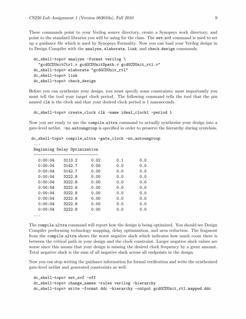
The compile ultra command will report how the design is being optimized. You should see DesignCompiler performing technology mapping, delay optimization, and area reduction. The fragmentfrom the compile ultra shows the worst negative slack which indicates how much room there isbetween the critical path in your design and the clock constraint. Larger negative slack values areworse since this means that your design is missing the desired clock frequency by a great amount.Total negative slack is the sum of all negative slack across all endpoints in the design.
Now you can stop writing the guidance information for formal verification and write the synthesizedgate-level netlist and generated constraints as well.
dc_shell-topo> set_svf -off
dc_shell-topo> change_names -rules verilog -hierarchy
dc_shell-topo> write -format ddc -hierarchy -output gcdGCDUnit_rtl.mapped.ddc

CS250 Lab Assignment 1 (Version 083010a), Fall 2010 10
dc_shell-topo> write -f verilog -hierarchy -output gcdGCDUnit_rtl.mapped.v
dc_shell-topo> write_sdf gcdGCDUnit_rtl.mapped.sdf
dc_shell-topo> write_sdc -nosplit gcdGCDUnit_rtl.mapped.sdc
dc_shell-topo> write_milkyway -overwrite -output "gcdGCDUnit_rtl_DCT"
dc_shell-topo> source ./find_regs.tcl
dc_shell-topo> find_regs gcdTestHarness_rtl/gcd
Take a look at various reports on synthesis results.
dc_shell-topo> report_timing -transition_time -nets -attributes -nosplit
...
Point Fanout Trans Incr Path
----------------------------------------------------------------------------
clock ideal_clock1 (rise edge) 0.00 0.00
clock network delay (ideal) 0.00 0.00
dpath/A_reg_reg_1_/CLK (DFFX1) 0.00 0.00 0.00 r
dpath/A_reg_reg_1_/Q (DFFX1) 0.05 0.19 0.19 f
dpath/out[1] (net) 5 0.00 0.19 f
dpath/U94/QN (NAND2X1) 0.05 0.03 0.22 r
dpath/n21 (net) 1 0.00 0.22 r
...
dpath/U60/QN (NAND2X1) 0.06 0.04 0.53 f
dpath/n97 (net) 1 0.00 0.53 f
dpath/U62/ZN (INVX2) 0.04 0.03 0.56 r
dpath/is_A_lt_B (net) 3 0.00 0.56 r
dpath/is_A_lt_B (gcdGCDUnitDpath_W16) 0.00 0.56 r
is_A_lt_B (net) 0.00 0.56 r
ctrl/is_A_lt_B (gcdGCDUnitCtrl) 0.00 0.56 r
ctrl/is_A_lt_B (net) 0.00 0.56 r
ctrl/U6/ZN (INVX2) 0.03 0.02 0.59 f
ctrl/n1 (net) 1 0.00 0.59 f
...
ctrl/U5/QN (NAND2X1) 0.05 0.02 0.78 r
ctrl/en_A (net) 1 0.00 0.78 r
ctrl/en_A (gcdGCDUnitCtrl) 0.00 0.78 r
en_A (net) 0.00 0.78 r
dpath/en_A (gcdGCDUnitDpath_W16) 0.00 0.78 r
dpath/en_A (net) 0.00 0.78 r
dpath/clk_gate_A_reg_reg/EN (SNPS_CLOCK_GATE_HIGH..) 0.00 0.78 r
dpath/clk_gate_A_reg_reg/EN (net) 0.00 0.78 r
dpath/clk_gate_A_reg_reg/latch/D (LATCHX1) 0.05 0.00 0.78 r
data arrival time 0.78
clock ideal_clock1’ (rise edge) 0.50 0.50
clock network delay (ideal) 0.00 0.50
dpath/clk_gate_A_reg_reg/latch/CLK (LATCHX1) 0.00 0.50 r
time borrowed from endpoint 0.28 0.78
data required time 0.78

CS250 Lab Assignment 1 (Version 083010a), Fall 2010 11
----------------------------------------------------------------------------
data required time 0.78
data arrival time 0.78
----------------------------------------------------------------------------
slack (MET) 0.00
...
This report lists the critical path of the design. The critical path is the slowest logic between anytwo registers and is therefore the limiting factor preventing you from decreasing the clock periodconstraint. You can see that the critical path starts at bit 1 of the operand A register in thedatapath; goes through the comparator; to the control logic; and finally ends at the clock gatelatch controlling the operand A register in the datapath. The critical path takes a total of 0.78nswhich is less than the 1ns clock period constraint.
dc_shell-topo> report_area -nosplit -hierarchy
...
Global cell area Local cell area
------------------ ----------------------------
Hierarchical cell Absolute Percent Combi- Noncombi- Black
Total Total national national boxes
------------------------ --------- ------- --------- --------- ------
gcdGCDUnit_rtl 2869.8560 100.0 0.0000 0.0000 0.0000
ctrl 193.5360 6.7 143.7696 49.7664 0.0000
dpath 2676.3206 93.3 1810.0188 796.2622 0.0000
dpath/clk_gate_A_reg_reg 35.0208 1.2 12.9024 22.1184 0.0000
dpath/clk_gate_B_reg_reg 35.0208 1.2 12.9024 22.1184 0.0000
------------------------ --------- ------- --------- --------- ------
Total 1979.5931 890.2654 0.0000
...
This report tells you the post synthesis area results. The units are um2. You can see that thedatapath consumes 93.3% of the total chip area.
dc_shell-topo> report_power -nosplit -hier
...
--------------------------------------------------------------------------
Switch Int Leak Total
Hierarchy Power Power Power Power %
--------------------------------------------------------------------------
gcdGCDUnit_rtl 380.908 689.568 1.39e+07 1.08e+03 100.0
dpath (gcdGCDUnitDpath_W16) 361.460 673.192 1.30e+07 1.05e+03 96.6
ctrl (gcdGCDUnitCtrl) 19.448 16.376 8.80e+05 36.704 3.4
...
This report tells you about post synthesis power results. The dynamic power units are uW whilethe leakage power units are pW .
dc_shell-topo> report_reference -nosplit -hierarchy
...

CS250 Lab Assignment 1 (Version 083010a), Fall 2010 12
****************************************
Design: gcdGCDUnitDpath_W16
****************************************
Reference Library Unit Area Count Total Area Attributes
-----------------------------------------------------------------------------
AND2X1 saed90nm_typ 7.372800 1 7.372800
AO21X1 saed90nm_typ 10.137600 1 10.137600
AO222X1 saed90nm_typ 14.745600 13 191.692797
AOI21X1 saed90nm_typ 11.980800 4 47.923199
AOI22X1 saed90nm_typ 12.902400 3 38.707200
DFFX1 saed90nm_typ 24.883200 32 796.262390 n
INVX0 saed90nm_typ 5.529600 28 154.828804
INVX2 saed90nm_typ 6.451200 1 6.451200
MUX21X1 saed90nm_typ 11.059200 16 176.947205
NAND2X0 saed90nm_typ 5.529600 7 38.707201
NAND2X1 saed90nm_typ 5.529600 67 370.483210
NAND3X0 saed90nm_typ 7.372800 2 14.745600
NAND4X0 saed90nm_typ 8.294400 3 24.883201
NOR2X0 saed90nm_typ 5.529600 31 171.417604
NOR2X2 saed90nm_typ 9.216000 4 36.863998
NOR3X0 saed90nm_typ 8.294400 2 16.588800
NOR4X0 saed90nm_typ 9.216000 5 46.079998
OA22X1 saed90nm_typ 11.059200 5 55.296001
OAI21X1 saed90nm_typ 11.059200 13 143.769604
OR2X1 saed90nm_typ 7.372800 3 22.118400
SNPS_CLOCK_GATE.. 35.020801 1 35.020801 h, n
SNPS_CLOCK_GATE.. 35.020801 1 35.020801 h, n
XNOR2X1 saed90nm_typ 13.824000 8 110.592003
XOR2X1 saed90nm_typ 13.824000 9 124.416003
-----------------------------------------------------------------------------
Total 24 references 2676.326418
...
This report lists the standard cells used in each module. The gcdGCDUnitDpath module is madeout of 32 DFFX1 cells, 67 NAND2X1 cells, etc. You can also see how much area it is consuming.
dc_shell-topo> report_resources -nosplit -hierarchy
...
Resource Report for this hierarchy in file ../../src/gcdGCDUnitDpath.v
=============================================================================
| Cell | Module | Parameters | Contained Operations |
=============================================================================
| sub_x_28_1 | DW01_sub | width=16 | sub_28 |
| lt_x_46_1 | DW_cmp | width=16 | lt_46 |
=============================================================================
Implementation Report
===============================================================================

CS250 Lab Assignment 1 (Version 083010a), Fall 2010 13
| | | Current | Set |
| Cell | Module | Implementation | Implementation |
===============================================================================
| sub_x_28_1 | DW01_sub | pparch (area,speed) |
| lt_x_46_1 | DW_cmp | apparch (area) | |
===============================================================================
...
Synopsys provides a library of commonly used arithmetic components as highly optimized buildingblocks. This library is called Design Ware and Design Compiler will automatically use DesignWare components when it can. This report can help you determine when Design Compiler is usingDesign Ware components. The DW01 sub in the module name indicates that this is a Design Waresubtractor. This report also gives you what type of architecutre it used.
You can use makefiles and scripts to help automate the process of synthesizing your design.
% cd $LABROOT/build/dc-syn
% cat Makefile
...
vsrcs = \
$(srcdir)/gcdGCDUnitCtrl.v \
$(srcdir)/gcdGCDUnitDpath.v \
$(srcdir)/gcdGCDUnit_rtl.v \
...
% make
Go ahead and take a look what the automated build system produced.
% cd $LABROOT/build/dc-syn
% ls -l
-rw-r--r-- 1 yunsup grad 4555 Aug 29 22:15 Makefile
drwxr-xr-x 7 yunsup grad 4096 Aug 29 22:15 build-dc-2010-08-29_22-15
-rw-r--r-- 1 yunsup grad 1108 Aug 28 12:06 constraints.tcl
lrwxrwxrwx 1 yunsup grad 25 Aug 29 22:15 current-dc -> build-dc-2010-08-29_22-15
drwxr-xr-x 2 yunsup grad 4096 Aug 29 21:39 rm_dc_scripts
drwxr-xr-x 2 yunsup grad 4096 Aug 28 12:00 rm_notes
drwxr-xr-x 2 yunsup grad 4096 Aug 29 21:50 rm_setup
% cd current-dc
% ls -l
drwxr-xr-x 2 yunsup grad 4096 Aug 29 22:15 WORK
-rw-r--r-- 1 yunsup grad 47 Aug 29 22:15 access.tab
-rw-r--r-- 1 yunsup grad 235827 Aug 29 22:15 command.log
-rw-r--r-- 1 yunsup grad 5141 Aug 29 22:15 common_setup.tcl
-rw-r--r-- 1 yunsup grad 1108 Aug 29 22:15 constraints.tcl
-rw-r--r-- 1 yunsup grad 18996 Aug 29 22:15 dc.tcl
-rw-r--r-- 1 yunsup grad 4621 Aug 29 22:15 dc_setup.tcl
-rw-r--r-- 1 yunsup grad 4625 Aug 29 22:15 dc_setup_filenames.tcl
-rw-r--r-- 1 yunsup grad 2730 Aug 29 22:15 find_regs.tcl
-rw-r--r-- 1 yunsup grad 4439 Aug 29 22:15 force_regs.ucli

CS250 Lab Assignment 1 (Version 083010a), Fall 2010 14
drwxr-xr-x 3 yunsup grad 4096 Aug 29 22:15 gcdGCDUnit_rtl_LIB
drwxr-xr-x 2 yunsup grad 4096 Aug 29 22:15 log
-rw-r--r-- 1 yunsup grad 1087 Aug 29 22:15 make_generated_vars.tcl
drwxr-xr-x 2 yunsup grad 4096 Aug 29 22:15 reports
drwxr-xr-x 2 yunsup grad 4096 Aug 29 22:15 results
-rw-r--r-- 1 yunsup grad 29 Aug 29 22:15 timestamp
Notice that the makefile does not overwrite build directories. It always create new build directories.This makes it easy to change your synthesis scripts or source Verilog, resynthesize your design, andcompare your results to previous designs. You can use symlinks to keep track of various builddirectories. Inside the current-dc directory, you can see all the tcl scripts as well as the directoriesnamed results and reports: results contains your synthesized gate-level netlist; and reports
contains various post synthesis reports.
Synopsys provides a GUI front-end for Design Compiler called Design Vision which you will use toanalyze the synthesis result. You should avoid using the GUI to actually perform synthesis sinceyou want to use scripts for this. Now launch design vision.
% cd $LABROOT/build/dc-syn/current-dc
% design_vision-xg -64bit
...
Initializing...
design_vision> alias "design_vision>" ""
design_vision> source dc_setup.tcl
design_vision> read_file -format ddc "results/gcdGCDUnit_rtl.mapped.ddc"
You can browse your design with the hierarchical view (see Figure 5). If you right click on amodule and choose Schematic View option, the tool will display a schematic of the synthesizedlogic corresponding to that module.
Synopsys Formality: Formal Verification
Formality formally verifies whether or not the RTL and the synthesized gate-level netlist match.
% cd $LABROOT/build.manual/dc-syn
% fm_shell -64bit
...
fm_shell (setup)> alias "fm_shell" ""
fm_shell (setup)> alias "(setup)>" ""
fm_shell (setup)> alias "(match)>" ""
fm_shell (setup)> alias "(verify)>" ""
Execute some commands to setup your environment.
fm_shell (setup)> set ucb_vlsi_home [getenv UCB_VLSI_HOME]
fm_shell (setup)> set stdcells_home \
$ucb_vlsi_home/stdcells/synopsys-90nm/default
fm_shell (setup)> set_app_var search_path \
"$stdcells_home/db ~cs250/install/vclib ../../src"

CS250 Lab Assignment 1 (Version 083010a), Fall 2010 15
Figure 5: Design Vision Hierarchical View
fm_shell (setup)> set_app_var synopsys_auto_setup "true"
fm_shell (setup)> set_svf "gcdGCDUnit_rtl.svf"
fm_shell (setup)> read_db -technology_library "cells.db"
These commands point to your Verilog source directory, the svf file you generated during synthesis,and point to the standard libraries you will be using for the class. Now you can load your originalRTL design and the synthesized gate-level netlist to Formality.
fm_shell (setup)> read_verilog -r \
"gcdGCDUnitCtrl.v gcdGCDUnitDpath.v gcdGCDUnit_rtl.v" \
-work_library WORK
fm_shell (setup)> set_top r:/WORK/gcdGCDUnit_rtl
fm_shell (setup)> read_ddc -i "./gcdGCDUnit_rtl.mapped.ddc"
fm_shell (setup)> set_top i:/WORK/gcdGCDUnit_rtl
You are ready to verify whether or not both design match.
fm_shell (setup)> match
fm_shell (match)> report_unmatched_points
fm_shell (match)> verify
...
************************* Verification Results *************************
Verification SUCCEEDED
ATTENTION: synopsys_auto_setup mode was enabled.
See Synopsys Auto Setup Summary for details
-----------------------------------------------------------
Reference design: r:/WORK/gcdGCDUnit_rtl
Implementation design: i:/WORK/gcdGCDUnit_rtl

CS250 Lab Assignment 1 (Version 083010a), Fall 2010 16
52 Passing compare points
------------------------------------------------------------------------
Matched Compare Points BBPin Loop BBNet Cut Port DFF LAT TOTAL
------------------------------------------------------------------------
Passing (equivalent) 0 0 0 0 18 34 0 52
Failing (not equivalent) 0 0 0 0 0 0 0 0
************************************************************************
...
You can also report the current status.
fm_shell (verify)> report_status
You can use makefiles and scripts to help automate the process of formal verification.
% cd $LABROOT/build/dc-syn
% make fm
Synopsys VCS: Simulating Post Synthesis Gate-Level Netlist
After obtaining the synthesized gate-level netlist, you will double-check the netlist by running asimulation using VCS.
% cd $LABROOT/build.manual/dc-syn
% sdfcorrect.py gcdGCDUnit_rtl.mapped.sdf gcdGCDUnit_rtl.mapped.corrected.sdf
% cd $LABROOT/build.manual/vcs-sim-gl-syn
% vcs -full64 -PP +lint=all +v2k -timescale=1ns/10ps \
-P ../dc-syn/access.tab -debug \
+neg_tchk +sdfverbose \
-sdf typ:gcdGCDUnit_rtl:../dc-syn/gcdGCDUnit_rtl.mapped.corrected.sdf \
+incdir+$UCB_VLSI_HOME/install/vclib \
-v $UCB_VLSI_HOME/install/vclib/vcQueues.v \
-v $UCB_VLSI_HOME/install/vclib/vcStateElements.v \
-v $UCB_VLSI_HOME/install/vclib/vcTest.v \
-v $UCB_VLSI_HOME/install/vclib/vcTestSource.v \
-v $UCB_VLSI_HOME/install/vclib/vcTestSink.v \
$UCB_VLSI_HOME/stdcells/synopsys-90nm/default/verilog/cells.v \
../dc-syn/gcdGCDUnit_rtl.mapped.v \
../../src/gcdTestHarness_rtl.v
% ./simv -ucli +verbose=1
ucli% source ../dc-syn/force_regs.ucli
ucli% run
...
+ Running Test Case: gcdGCDUnit_rtl
[ passed ] Test ( vcTestSink ) succeeded, [ 0003 == 0003 ]
[ passed ] Test ( vcTestSink ) succeeded, [ 0007 == 0007 ]
[ passed ] Test ( vcTestSink ) succeeded, [ 0005 == 0005 ]
[ passed ] Test ( vcTestSink ) succeeded, [ 0001 == 0001 ]
[ passed ] Test ( vcTestSink ) succeeded, [ 0028 == 0028 ]

CS250 Lab Assignment 1 (Version 083010a), Fall 2010 17
[ passed ] Test ( vcTestSink ) succeeded, [ 000a == 000a ]
[ passed ] Test ( vcTestSink ) succeeded, [ 0005 == 0005 ]
[ passed ] Test ( vcTestSink ) succeeded, [ 0000 == 0000 ]
[ passed ] Test ( Is sink finished? ) succeeded
...
You can use the makefile to build the post synthesis gate-level netlist simulator and run the simu-lator.
% cd $LABROOT/build/vcs-sim-gl-syn
% make
% make run
Synopsys IC Compiler: Gate-Level Netlist to Layout
IC Compiler performs place and route. This tool takes a synthesized gate-level netlist and astandard cell library as input and produces a layout as an output. At this point, you can see theinstantiated standard cells and routed metals. You will use this tool more interactively, so go aheadand launch the IC Compiler with the GUI enabled.
% cd $LABROOT/build.manual/icc-par
% icc_shell -64bit -gui
...
Initializing...
icc_shell> alias "icc_shell>" ""
Execute some commands to setup your environment.
icc_shell> set ucb_vlsi_home [getenv UCB_VLSI_HOME]
icc_shell> set stdcells_home \
$ucb_vlsi_home/stdcells/synopsys-90nm/default
icc_shell> set_app_var search_path "$stdcells_home/db"
icc_shell> set_app_var target_library "cells.db"
icc_shell> set_app_var link_library "* $target_library"
These commands point to the standard libraries you will be using for the class. Before you jumpinto place and route, you will create your own Milkyway database, the place where you will besaving your place and routed design. Notice while you create the Milkyway database you hand inthe technology file which has all the information about the process (e.g., detailed information ofthe poly and the metal layers), and the Milkyway reference database which captures the standardcell layout. Then you will read your synthesized gate-level netlist from the dc-syn directory. Alsospecify the tlu+ files which has the information you will use when extracting the parasitics of thelayout. You will also make power and ground ports.
icc_shell> create_mw_lib \
-tech "$stdcells_home/techfile/techfile.tf" \
-bus_naming_style {[%d]} \
-mw_reference_library "$stdcells_home/mw/cells.mw" \
"gcdGCDUnit_rtl_LIB"
CS250 Lab Assignment 1 (Version 083010a), Fall 2010 18
icc_shell> open_mw_lib gcdGCDUnit_rtl_LIB
icc_shell> import_designs "../dc-syn/gcdGCDUnit_rtl.mapped.ddc" \
-format "ddc" -top "gcdGCDUnit_rtl" -cel "gcdGCDUnit_rtl"
icc_shell> set_tlu_plus_files \
-max_tluplus "$stdcells_home/tluplus/max.tluplus" \
-min_tluplus "$stdcells_home/tluplus/min.tluplus" \
-tech2itf_map "$stdcells_home/techfile/tech2itf.map"
icc_shell> derive_pg_connection \
-power_net "VDD" -power_pin "VDD" -ground_net "VSS" -ground_pin "VSS" \
-create_ports "top"
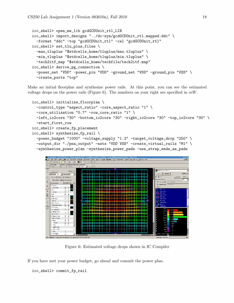
Make an initial floorplan and synthesize power rails. At this point, you can see the estimatedvoltage drops on the power rails (Figure 6). The numbers on your right are specified in mW .
icc_shell> initialize_floorplan \
-control_type "aspect_ratio" -core_aspect_ratio "1" \
-core_utilization "0.7" -row_core_ratio "1" \
-left_io2core "30" -bottom_io2core "30" -right_io2core "30" -top_io2core "30" \
-start_first_row
icc_shell> create_fp_placement
icc_shell> synthesize_fp_rail \
-power_budget "1000" -voltage_supply "1.2" -target_voltage_drop "250" \
-output_dir "./pna_output" -nets "VDD VSS" -create_virtual_rails "M1" \
-synthesize_power_plan -synthesize_power_pads -use_strap_ends_as_pads
Figure 6: Estimated voltage drops shown in IC Compiler
If you have met your power budget, go ahead and commit the power plan.
icc_shell> commit_fp_rail
CS250 Lab Assignment 1 (Version 083010a), Fall 2010 19
You will now perform clock tree synthesis. Because the clock is one of the highest fan-out nets, youshould route this signal first. The tool will first analyze the clock net and insert buffers to minimizethe skew before routing.
icc_shell> clock_opt -only_cts -no_clock_route
icc_shell> route_zrt_group -all_clock_nets -reuse_existing_global_route true
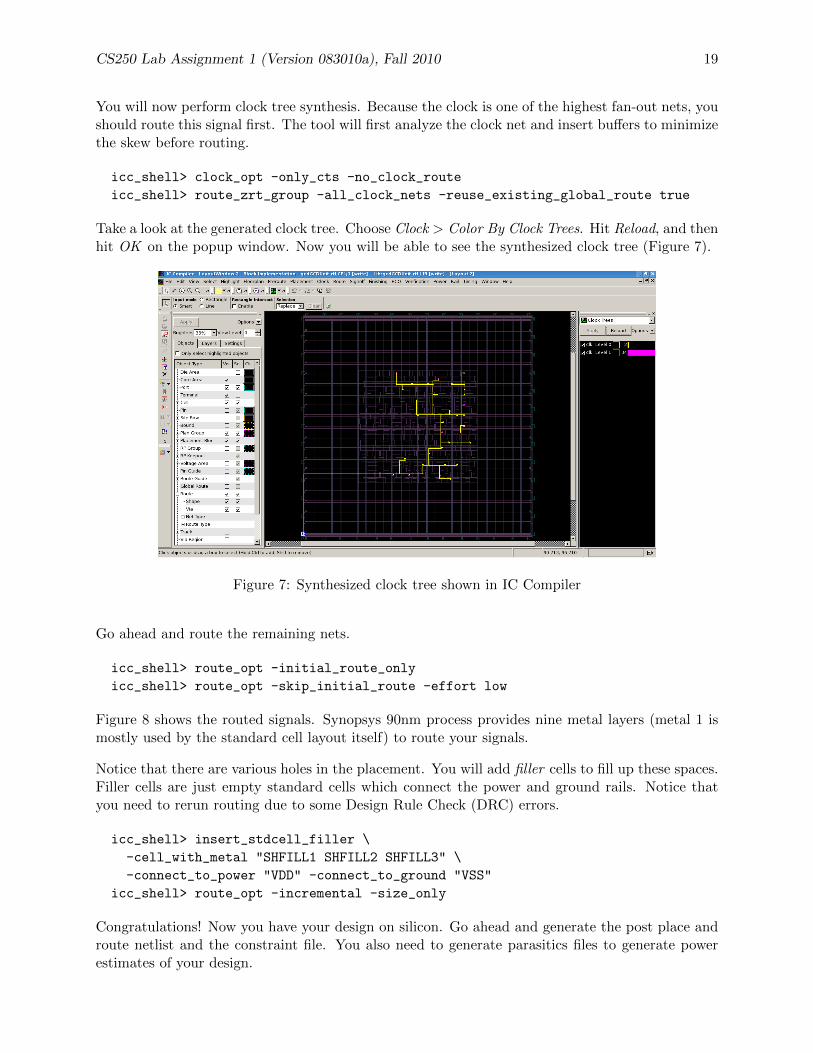
Take a look at the generated clock tree. Choose Clock > Color By Clock Trees. Hit Reload, and thenhit OK on the popup window. Now you will be able to see the synthesized clock tree (Figure 7).
Figure 7: Synthesized clock tree shown in IC Compiler
Go ahead and route the remaining nets.
icc_shell> route_opt -initial_route_only
icc_shell> route_opt -skip_initial_route -effort low
Figure 8 shows the routed signals. Synopsys 90nm process provides nine metal layers (metal 1 ismostly used by the standard cell layout itself) to route your signals.
Notice that there are various holes in the placement. You will add filler cells to fill up these spaces.Filler cells are just empty standard cells which connect the power and ground rails. Notice thatyou need to rerun routing due to some Design Rule Check (DRC) errors.
icc_shell> insert_stdcell_filler \
-cell_with_metal "SHFILL1 SHFILL2 SHFILL3" \
-connect_to_power "VDD" -connect_to_ground "VSS"
icc_shell> route_opt -incremental -size_only
Congratulations! Now you have your design on silicon. Go ahead and generate the post place androute netlist and the constraint file. You also need to generate parasitics files to generate powerestimates of your design.

CS250 Lab Assignment 1 (Version 083010a), Fall 2010 20
Figure 8: Routed signals shown in IC Compiler
icc_shell> change_names -rules verilog -hierarchy
icc_shell> write_verilog "gcdGCDUnit_rtl.output.v"
icc_shell> write_sdf "gcdGCDUnit_rtl.output.sdf"
icc_shell> write_sdc "gcdGCDUnit_rtl.output.sdc"
icc_shell> extract_rc -coupling_cap
icc_shell> write_parasitics -format SBPF -output "gcdGCDUnit_rtl.output.sbpf"
icc_shell> source ./find_regs.tcl
icc_shell> find_regs gcdTestHarness_rtl/gcd
icc_shell> save_mw_cel
icc_shell> close_mw_cel
You can automate this process. Notice that the makefile creates new build directories like the onein Design Compiler.
% cd $LABROOT/build/icc-par
% make
% ls -l
-rw-r--r-- 1 yunsup grad 15232 Aug 28 18:40 Makefile
drwxr-xr-x 6 yunsup grad 4096 Aug 29 23:42 build-icc-2010-08-29_23-41
drwxr-xr-x 8 yunsup grad 4096 Aug 29 23:41 build-iccdp-2010-08-29_23-41
lrwxrwxrwx 1 yunsup grad 26 Aug 29 23:41 current-icc -> build-icc-2010-08-29_23-41
lrwxrwxrwx 1 yunsup grad 28 Aug 29 23:41 current-iccdp -> build-iccdp-2010-08-29_23-41
drwxr-xr-x 2 yunsup grad 4096 Aug 29 23:19 rm_icc_dp_scripts
drwxr-xr-x 2 yunsup grad 4096 Aug 29 23:29 rm_icc_scripts
drwxr-xr-x 2 yunsup grad 4096 Aug 29 23:38 rm_icc_zrt_scripts
drwxr-xr-x 2 yunsup grad 4096 Aug 28 16:20 rm_notes
drwxr-xr-x 2 yunsup grad 4096 Aug 29 23:34 rm_setup

CS250 Lab Assignment 1 (Version 083010a), Fall 2010 21
Synopsys VCS: Simulating Post Place and Route Gate-Level Netlist
After you obtain the post place and route gate-level netlist, you will double-check the netlist byrunning a simulation using VCS. You also need to get the switching activities in several formats toestimate power. Use vpd2vcd and vcd2saif to convert a vpd format into a vcd and a saif format.
% cd $LABROOT/build.manual/icc-par
% sdfcorrect.py gcdGCDUnit_rtl.output.sdf gcdGCDUnit_rtl.output.corrected.sdf
% cd $LABROOT/build.manual/vcs-sim-gl-par
% vcs -full64 -PP +lint=all +v2k -timescale=1ns/10ps \
-P ../icc-par/access.tab -debug \
+neg_tchk +sdfverbose \
-sdf typ:gcdGCDUnit_rtl:../icc-par/gcdGCDUnit_rtl.output.corrected.sdf \
+incdir+$UCB_VLSI_HOME/install/vclib \
-v $UCB_VLSI_HOME/install/vclib/vcQueues.v \
-v $UCB_VLSI_HOME/install/vclib/vcStateElements.v \
-v $UCB_VLSI_HOME/install/vclib/vcTest.v \
-v $UCB_VLSI_HOME/install/vclib/vcTestSource.v \
-v $UCB_VLSI_HOME/install/vclib/vcTestSink.v \
$UCB_VLSI_HOME/stdcells/synopsys-90nm/default/verilog/cells.v \
../icc-par/gcdGCDUnit_rtl.output.v \
../../src/gcdTestHarness_rtl.v
% ./simv -ucli +verbose=1
ucli% source ../icc-par/force_regs.ucli
ucli% run
...
+ Running Test Case: gcdGCDUnit_rtl
[ passed ] Test ( vcTestSink ) succeeded, [ 0003 == 0003 ]
[ passed ] Test ( vcTestSink ) succeeded, [ 0007 == 0007 ]
[ passed ] Test ( vcTestSink ) succeeded, [ 0005 == 0005 ]
[ passed ] Test ( vcTestSink ) succeeded, [ 0001 == 0001 ]
[ passed ] Test ( vcTestSink ) succeeded, [ 0028 == 0028 ]
[ passed ] Test ( vcTestSink ) succeeded, [ 000a == 000a ]
[ passed ] Test ( vcTestSink ) succeeded, [ 0005 == 0005 ]
[ passed ] Test ( vcTestSink ) succeeded, [ 0000 == 0000 ]
[ passed ] Test ( Is sink finished? ) succeeded
...
% vpd2vcd vcdplus.vpd vcdplus.vcd
% vcd2saif -input vcdplus.vcd -output vcdplus.saif
You can use the makefile to build the post synthesis gate-level netlist simulator, run, and convertthe switching activity file into a vcd and a saif format.
% cd $LABROOT/build/vcs-sim-gl-par
% make
% make run
% make convert

CS250 Lab Assignment 1 (Version 083010a), Fall 2010 22
Synopsys PrimeTime PX: Estimating Power
PrimeTime PX is an add-on feature to PrimeTime that analyzes power dissipation of a cell-baseddesign. PrimeTime PX supports two types of power analysis modes. They are averaged mode andtime-based mode. Averaged mode calculates averaged power based on toggle rates. Time-basedmode let’s you know the peak power as well as the averaged power using gate-level simulationactivity.
% cd $LABROOT/build.manual/pt-pwr
% pt_shell -64bit
...
pt_shell> alias "pt_shell>" ""
Go ahead and execute some commands to setup your environment. Enable the power analysismode.
pt_shell> set ucb_vlsi_home [getenv UCB_VLSI_HOME]
pt_shell> set stdcells_home \
$ucb_vlsi_home/stdcells/synopsys-90nm/default
pt_shell> set search_path "$stdcells_home/db"
pt_shell> set target_library "cells.db"
pt_shell> set link_path "* $target_library"
pt_shell> set power_enable_analysis "true"
Read the post place and route gate-level netlist into PrimeTime PX.
pt_shell> read_verilog "../icc-par/gcdGCDUnit_rtl.output.v"
pt_shell> current_design "gcdGCDUnit_rtl"
pt_shell> link
Start with the averaged mode power analysis. This mode uses the saif format. Read the parasiticsgenerated by IC Compiler before you run report power.
pt_shell> set power_analysis_mode "averaged"
pt_shell> read_saif "../vcs-sim-gl-par/vcdplus.saif" \
-strip_path "gcdTestHarness_rtl/gcd"
pt_shell> report_switching_activity -list_not_annotated
pt_shell> read_parasitics -increment \
-format sbpf "../icc-par/gcdGCDUnit_rtl.output.sbpf.max"
pt_shell> report_power -verbose -hierarchy
...
Switch Int Leak Total
Hierarchy Power Power Power Power %
---------------------------------------------------------------------------
gcdGCDUnit_rtl 9.48e-05 9.48e-05 1.52e-05 2.05e-04 100.0
dpath (gcdGCDUnitDpath_W16) 8.29e-05 6.67e-05 1.42e-05 1.64e-04 80.0
clk_gate_A_reg_reg (SNPS_CLOCK_GATE_HIGH_gcdGCDUnitDpath_W16_1)
3.14e-05 1.35e-05 2.22e-07 4.52e-05 22.1
clk_gate_B_reg_reg (SNPS_CLOCK_GATE_HIGH_gcdGCDUnitDpath_W16_0)

CS250 Lab Assignment 1 (Version 083010a), Fall 2010 23
3.14e-05 1.27e-05 2.22e-07 4.44e-05 21.7
ctrl (gcdGCDUnitCtrl) 1.19e-05 2.81e-05 9.46e-07 4.09e-05 20.0
...
You can see the average power consumption by each module in your design.
Try the time-based power analysis. This mode takes the vcd format as an input. Read the parasiticsand run report power. You will see the estimated peak power as well as the average power.
pt_shell> set power_analysis_mode "time_based"
pt_shell> read_vcd "../vcs-sim-gl-par/vcdplus.vcd" \
-strip_path "gcdTestHarness_rtl/gcd"
pt_shell> report_switching_activity -list_not_annotated
pt_shell> read_parasitics -increment \
-format sbpf "../icc-par/gcdGCDUnit_rtl.output.sbpf.max"
pt_shell> report_power -verbose -hierarchy
...
Switch Int Leak Total
Hierarchy Power Power Power Power %
---------------------------------------------------------------------------
gcdGCDUnit_rtl 1.37e-04 1.05e-04 1.51e-05 2.57e-04 100.0
dpath (gcdGCDUnitDpath_W16) 1.21e-04 7.69e-05 1.42e-05 2.12e-04 82.3
clk_gate_A_reg_reg (SNPS_CLOCK_GATE_HIGH_gcdGCDUnitDpath_W16_1)
4.62e-05 1.33e-05 2.22e-07 5.96e-05 23.2
clk_gate_B_reg_reg (SNPS_CLOCK_GATE_HIGH_gcdGCDUnitDpath_W16_0)
4.80e-05 1.21e-05 2.22e-07 6.03e-05 23.4
ctrl (gcdGCDUnitCtrl) 1.67e-05 2.79e-05 9.37e-07 4.54e-05 17.7
Peak Peak Glitch X-tran
Hierarchy Power Time Power Power
---------------------------------------------------------------------------
gcdGCDUnit_rtl 1.49e-02 72.000-72.001 3.19e-07 7.61e-09
dpath (gcdGCDUnitDpath_W16) 9.05e-03 173.325-173.326 2.29e-07 0.000
clk_gate_A_reg_reg (SNPS_CLOCK_GATE_HIGH_gcdGCDUnitDpath_W16_1)
2.69e-03 129.999-130.000 2.78e-09 0.000
clk_gate_B_reg_reg (SNPS_CLOCK_GATE_HIGH_gcdGCDUnitDpath_W16_0)
2.71e-03 49.999-50.000 0.000 0.000
ctrl (gcdGCDUnitCtrl) 9.44e-03 27.999-28.000 9.05e-08 7.61e-09
...
You can automate this process using makefiles.
% cd $LABROOT/build/pt-pwr
% make

CS250 Lab Assignment 1 (Version 083010a), Fall 2010 24
Lab Hints and Tips
Tip 1: Write clean synthesizable code
Place most of your logic in leaf modules and use structural Verilog to connect the leaf modules ina hierarchy. Make sure to separate out datapath and control circuitry.
Tip 2: Make Use of the Verilog Component Library
We have provided you with a very simple Verilog Component Library (VCLIB) which you mayfind useful for this lab. VCLIB includes queue control logic, and memory modules. It is installedglobally at ~cs250/install/vclib. Examine the makefile included in the lab harness to see howto link in the library.
Tip 3: Write Semi-Behavioral Verilog
You might try to design optimized gate-level comparators and a subtractor like the following.
vcEQComparator#(16) comp
(
.in0 (B),
.in1 (const0),
.out (B_zero)
);
vcLTComparator#(16) lt_comp
(
.in0 (A),
.in1 (B),
.out (A_lt_B)
);
vcSubtractor#(16) sub
(
.in0 (A),
.in1 (B),
.out (sub_out)
);
Consider using a more behavioral implementation of the functional units. The synthesize toolsmight pick up built in Verilog operators and use DesignWare components that might end up in amore efficient design.
assign B_zero = ( B == 0 );
assign A_lt_B = ( A < B );
assign sub_out = A - B;

CS250 Lab Assignment 1 (Version 083010a), Fall 2010 25
Questions
Your writing should not exceed one page. Make your writings as crisp as you can!
Q1. gcdGCDUnit
Tell us how your gcdGCDUnit works in detail. You might include a diagram of your datapath andcontrol logic.
Q2. W=16 vs. W=32
Throughout the lab, you assumed operand A, B, and the result to be 16 bits wide. We would liketo make a GCD unit which takes 32 bits operands and produces a 32 bit result.
• What changes would be necessary for the gcdGCDUnit rtl module?
• Does the Verilog test harness gcdTestHarness rtl work? If not, what changes do youneed to make in order to test our new 32-bit gcdGCDUnit rtl? Show us that your 32-bitgcdGCDUnit rtl works.
• How does this affect your chip? Explain by filling in the following table. Write a pythonscript which goes through all the generated reports. You should be able to run a script likethe following and simplify fill in the table. Commit the script to the repository.
% cd $LABROOT/build
% ./collect_data.py
Unit gcdGCDUnit rtl (W=16) gcdGCDUnit rtl (W=32)
Post Synthesis nsCritical Path Length
Post Synthesis um2
Area
Post Synthesis mWPower
Post Place+Route nsCritical Path Length
Post Place+Route um2
Area
Post Place+Route mWPower
Average Power (max) mW
Peak Power (max) mW
Total Cell Count(exclude SHFILL2 Cell)
DFFX* Cell Count
Q3. VLSI Tools
Tell us about your experience using the VLSI tools. Did you have any problems checking out alicense for any of the tools? Any suggestions?

CS250 Lab Assignment 1 (Version 083010a), Fall 2010 26
Read me before you commit!
• As you may have learned in this lab, makefiles for Design Compiler, IC Compiler, PrimeTimePX makes a new build directory for every new run. Don’t submit all of them. Make surethat you only turn in the most recent build result.
• You don’t need to submit results for the VCS simulation. We will build and run simulationbased on your committed source code or gate-level netlist. If you have added Verilog sourcescodes or changed the name of the Verilog source codes, however, you must commit themakefile for every vcs-sim-* directory.
• You don’t need to submit build results which are done manually.
• We will checkout the stuff you committed to the lab1/trunk and use that for lab grading.Feel free to take advantage of branches and tags. We will also checkout the version whichwas committed just before 10:30am on Monday, September 13. Use your late days wisely!
• To summarize, your SVN tree for lab1 should look like the following:
/yunsup
/lab1
/trunk
/src: COMMIT CODE
/build: COMMIT PYTHON SCRIPT
/dc-syn: COMMIT THE MOST RECENT VERSION
/icc-par: COMMIT THE MOST RECENT VERSION
/pt-pwr: COMMIT THE MOST RECENT VERSION
/vcs-sim-behav: commit if makefile has changed
/vcs-sim-gl-par: commit if makefile has changed
/vcs-sim-gl-syn: commit if makefile has changed
/vcs-sim-rtl: commit if makefile has changed
/build.manual: don’t commit stuff here
/writeup: COMMIT REPORT
/branches: feel free to use branches!
/tags: feel free to use tags!
Acknowledgements
Many people have contributed to versions of this lab over the years. The lab was originally developedfor CS250 VLSI Systems Design course at University of California at Berkeley by Yunsup Lee.Contributors include: Krste Asanovic, Christopher Batten, John Lazzaro, and John Wawrzynek.Versions of this lab have been used in the following courses:
• CS250 VLSI Systems Design (2009-2010) - University of California at Berkeley
• CSE291 Manycore System Design (2009) - University of California at San Diego