graphene-based tunable hyperbolic metamaterials and ...capolino.eng.uci.edu/publications_papers...
TRANSCRIPT
Graphene-based tunable hyperbolicmetamaterials and enhanced near-field
absorption
Mohamed A. K. Othman, Caner Guclu, and Filippo Capolino∗
Department of Electrical Engineering and Computer Science, University of California, Irvine,CA, 92697, USA
Abstract: We investigate a novel implementation of hyperbolic metama-terial (HM) at far-infrared frequencies composed of stacked graphene sheetsseparated by thin dielectric layers. Using the surface conductivity model ofgraphene, we derive the homogenization formula for the multilayer structureby treating graphene sheets as lumped layers with complex admittances.Homogenization results and limits are investigated by comparison with atransfer matrix formulation for the HM constituent layers. We show thatinfrared iso-frequency wavevector dispersion characteristics of the proposedHM can be tuned by varying the chemical potential of the graphene sheetsvia electrostatic biasing. Accordingly, reflection and transmission propertiesfor a film made of graphene-dielectric multilayer are tunable at terahertzfrequencies, and we investigate the limits in using the homogenized modelcompared to the more accurate transfer matrix model. We also propose touse graphene-based HM as a super absorber for near-fields generated at itssurface. The power emitted by a dipole near the surface of a graphene-basedHM is increased dramatically (up to 5 × 10² at 2 THz), furthermore weshow that most of the scattered power is directed into the HM. The validityand limits of the homogenized HM model are assessed also for near-fieldsand show that in certain conditions it overestimates the dipole radiatedpower into the HM.
© 2013 Optical Society of America
OCIS codes: (160.3918) Metamaterials; (230.4170) Multilayers; (250.5403) Plasmonics;(240.0310) Thin films.
References and links1. L. Felsen and N. Marcuvitz, Radiation and Scattering of Waves (Prentice-Hall, NJ, 1973).2. D. R. Smith and D. Schurig, “Electromagnetic wave propagation in media with indefinite permittivity and per-
meability tensors,” Phys. Rev. Lett. 90, 077405 (2003).3. C. Guclu, S. Campione, and F. Capolino, “Hyperbolic metamaterial as super absorber for scattered fields gener-
ated at its surface,” Phys. Rev. B 86, 205130 (2012).4. Y. Guo, W. Newman, C. Cortes, and Z. Jacob, “Applications of hyperbolic metamaterial substrates,” Adv. Opto-
Electron. 2012, 452502 (2012).5. Y. Guo, C. L. Cortes, S. Molesky, and Z. Jacob, “Broadband super-planckian thermal emission from hyperbolic
metamaterials,” Appl. Phys. Lett. 101, 131106 (2012).6. Z. Jacob, I. I. Smolyaninov, and E. E. Narimanov, “Broadband purcell effect: Radiative decay engineering with
metamaterials,” Appl. Phys. Lett. 100, 181105 (2012).7. I. Smolyaninov and E. Narimanov, “Metric signature transitions in optical metamaterials,” Phys. Rev. Lett. 105,
67402 (2010).
#182584 - $15.00 USD Received 2 Jan 2013; revised 12 Feb 2013; accepted 3 Mar 2013; published 20 Mar 2013(C) 2013 OSA 25 March 2013 / Vol. 21, No. 6 / OPTICS EXPRESS 7614
8. O. Kidwai, S. V. Zhukovsky, and J. E. Sipe, “Dipole radiation near hyperbolic metamaterials: applicability ofeffective-medium approximation,” Opt. Lett. 36, 2530–2532 (2011).
9. T. U. Tumkur, J. K. Kitur, B. Chu, L. Gu, V. A. Podolskiy, E. E. Narimanov, and M. A. Noginov, “Controlof reflectance and transmittance in scattering and curvilinear hyperbolic metamaterials,” Appl. Phys. Lett. 101,091105 (2012).
10. J. Pendry and S. Ramakrishna, “Refining the perfect lens,” Physica B: Condensed Matter 338, 329 – 332 (2003).11. K. J. Webb and M. Yang, “Subwavelength imaging with a multilayer silver film structure,” Opt. Lett. 31, 2130–
2132 (2006).12. T. Tumkur, L. Gu, J. Kitur, E. Narimanov, and M. Noginov, “Control of absorption with hyperbolic metamateri-
als,” Appl. Phys. Lett. 100, 161103–161103 (2012).13. A. N. Poddubny, P. A. Belov, P. Ginzburg, A. V. Zayats, and Y. S. Kivshar, “Microscopic model of purcell
enhancement in hyperbolic metamaterials,” Phys. Rev. B 86, 035148 (2012).14. C. L. Cortes, W. Newman, S. Molesky, and Z. Jacob, “Quantum nanophotonics using hyperbolic metamaterials,”
J. Opt. 14, 063001 (2012).15. G. V. Naik, J. Liu, A. V. Kildishev, V. M. Shalaev, and A. Boltasseva, “Demonstration of al:zno as a plasmonic
component for near-infrared metamaterials,” PNAS 109, 8834–8838 (2012).16. J. Kim, V. Drachev, Z. Jacob, G. Naik, A. Boltasseva, E. Narimanov, and V. Shalaev, “Improving the radiative
decay rate for dye molecules with hyperbolic metamaterials,” Opt. Express 20, 8100–8116 (2012).17. G. Naik and A. Boltasseva, “Semiconductors for plasmonics and metamaterials,” Phys. Status Solidi Rapid Res.
Lett. 4, 295–297 (2010).18. C. Rizza, A. Ciattoni, E. Spinozzi, and L. Columbo, “Terahertz active spatial filtering through optically tunable
hyperbolic metamaterials,” Opt. Lett. 37, 3345–3347 (2012).19. A. Vakil and N. Engheta, “One-atom-thick reflectors for surface plasmon polariton surface waves on graphene,”
Opt. Comm. 285, 3428 – 3430 (2012).20. F. Rana, “Graphene terahertz plasmon oscillators,” IEEE Trans. Nanotechnol. 7, 91–99 (2008).21. G. W. Hanson, A. B. Yakovlev, and A. Mafi, “Excitation of discrete and continuous spectrum for a surface
conductivity model of graphene,” J. Appl. Phys. 110, 114305 (2011).22. M. Tamagnone, J. Gomez-Diaz, J. Mosig, and J. Perruisseau-Carrier, “Analysis and design of terahertz antennas
based on plasmonic resonant graphene sheets,” J. Appl. Phys. 112, 114915 (2012).23. B. Wang, X. Zhang, F. J. Garcia-Vidal, X. Yuan, and J. Teng, “Strong coupling of surface plasmon polaritons in
monolayer graphene sheet arrays,” Phys. Rev. Lett. 109, 073901 (2012).24. I. V. Iorsh, I. S. Mukhin, I. V. Shadrivov, P. A. Belov, and Y. S. Kivshar, “Hyperbolic metamaterials based on
multilayer graphene structures,” Phys. Rev. B 87, 075416 (2013).25. A. Andryieuski, A. V. Lavrinenko, and D. N. Chigrin, “Graphene hyperlens for terahertz radiation,” Phys. Rev.
B 86, 121108 (2012).26. V. P. Gusynin and S. G. Sharapov, “Unconventional integer quantum hall effect in graphene,” Phys. Rev. Lett.
95, 146801 (2005).27. A. B. Kuzmenko, E. van Heumen, F. Carbone, and D. van der Marel, “Universal optical conductance of graphite,”
Phys. Rev. Lett. 100, 117401 (2008).28. L. Gerhard, E. Moyen, T. Balashov, I. Ozerov, M. Portail, H. Sahaf, L. Masson, W. Wulfhekel, and M. Hanbucken,
“A graphene electron lens,” Appl. Phys. Lett. 100, 153106 (2012).29. A. Vakil and N. Engheta, “Transformation optics using graphene,” Science 332, 1291–1294 (2011).30. C. Chen, S. Rosenblatt, K. Bolotin, W. Kalb, P. Kim, I. Kymissis, H. Stormer, T. Heinz, and J. Hone, “Perfor-
mance of monolayer graphene nanomechanical resonators with electrical readout,” Nature Nanotech. 4, 861–867(2009).
31. X. Wang, L. Zhi, and K. Mullen, “Transparent, conductive graphene electrodes for dye-sensitized solar cells,”Nano Lett. 8, 323–327 (2008).
32. C. S. R. Kaipa, G. W. P. Y. R. Yakovlev, Alexander Hanson, and M. F. Medina, F., “Enhanced transmission witha graphene-dielectric microstructure at low-terahertz frequencies,” Phys. Rev. B 85, 245407 (2012).
33. S. Thongrattanasiri, F. H. L. Koppens, and F. J. Garcia de Abajo, “Complete optical absorption in periodicallypatterned graphene,” Phys. Rev. Lett. 108, 047401 (2012).
34. A. Fallahi and J. Perruisseau-Carrier, “Design of tunable biperiodic graphene metasurfaces,” Phys. Rev. B 86,195408 (2012).
35. D. Sounas and C. Caloz, “Gyrotropy and nonreciprocity of graphene for microwave applications,” IEEE Trans.Microw. Theory Techn. 60, 901 –914 (2012).
36. D. L. Sounas and C. Caloz, “Electromagnetic nonreciprocity and gyrotropy of graphene,” Appl. Phys. Lett. 98,021911 (2011).
37. G. Lovat, “Equivalent circuit for electromagnetic interaction and transmission through graphene sheets,” IEEETrans. Electromagn. Compat. 54, 101 –109 (2012).
38. J. Sun, J. Zhou, B. Li, and F. Kang, “Indefinite permittivity and negative refraction in natural material: Graphite,”Appl. Phys. Lett. 98, 101901 (2011).
39. C. S. Kaipa, A. B. Yakovlev, F. Medina, F. Mesa, C. Butler, and A. P. Hibbins, “Circuit modeling of the trans-
#182584 - $15.00 USD Received 2 Jan 2013; revised 12 Feb 2013; accepted 3 Mar 2013; published 20 Mar 2013(C) 2013 OSA 25 March 2013 / Vol. 21, No. 6 / OPTICS EXPRESS 7615
missivity of stacked two-dimensional metallic meshes,” Opt. Express 18, 13309–13320 (2010).40. Y. R. Padooru, A. B. Yakovlev, C. S. Kaipa, F. Medina, and F. Mesa, “Circuit modeling of multiband high-
impedance surface absorbers in the microwave regime,” Phys. Rev. B 84, 035108 (2011).41. C. S. R. Kaipa, A. B. Yakovlev, F. Medina, and F. Mesa, “Transmission through stacked 2d periodic distributions
of square conducting patches,” J. Appl. Phys. 112, 033101 (2012).42. X. Ni, G. Naik, A. Kildishev, Y. Barnakov, A. Boltasseva, and V. Shalaev, “Effect of metallic and hyperbolic
metamaterial surfaces on electric and magnetic dipole emission transitions,” Appl. Phys. B 103, 553–558 (2011).43. K. Novoselov, A. Geim, S. Morozov, D. Jiang, Y. Zhang, S. Dubonos, I. Grigorieva, and A. Firsov, “Electric field
effect in atomically thin carbon films,” Science 306, 666–669 (2004).44. V. P. Gusynin, S. G. Sharapov, and J. P. Carbotte, “Sum rules for the optical and hall conductivity in graphene,”
Phys. Rev. B 75, 165407 (2007).45. G. W. Hanson, “Dyadic green’s functions and guided surface waves for a surface conductivity model of
graphene,” J. Appl. Phys. 103, 064302 (2008).46. R. A. Jishi, M. S. Dresselhaus, and G. Dresselhaus, “Electron-phonon coupling and the electrical conductivity of
fullerene nanotubules,” Phys. Rev. B 48, 11385–11389 (1993).47. Y.-W. Tan, Y. Zhang, K. Bolotin, Y. Zhao, S. Adam, E. H. Hwang, S. Das Sarma, H. L. Stormer, and P. Kim,
“Measurement of scattering rate and minimum conductivity in graphene,” Phys. Rev. Lett. 99, 246803 (2007).48. D. Pozar, Microwave engineering (John Wiley & Sons, 2009).49. O. Kidwai, S. V. Zhukovsky, and J. E. Sipe, “Effective-medium approach to planar multilayer hyperbolic meta-
materials: Strengths and limitations,” Phys. Rev. A 85, 053842 (2012).50. H. N. S. Krishnamoorthy, Z. Jacob, E. Narimanov, I. Kretzschmar, and V. M. Menon, “Topological transitions in
metamaterials,” Science 336, 205–209 (2012).51. S. Campione, S. Steshenko, M. Albani, and F. Capolino, “Complex modes and effective refractive index in 3d
periodic arrays of plasmonic nanospheres,” Opt. Express 19, 26027–26043 (2011).52. F. Capolino and M. Albani, “Truncation effects in a semi-infinite periodic array of thin strips: A discrete wiener-
hopf formulation,” Radio Sci. 44, RS2S91 (2009).53. P.-Y. Chen and A. Alu, “Atomically thin surface cloak using graphene monolayers,” ACS Nano 5, 5855–5863
(2011).54. Z. Jacob, J. Kim, G. Naik, A. Boltasseva, E. Narimanov, and V. Shalaev, “Engineering photonic density of states
using metamaterials,” Appl. Phys. B 100, 215–218 (2010).
1. Introduction
A stack of graphene sheets, separated by subwavelength dielectric spacers, can be regarded as acomposite material with uniaxial electric properties under certain conditions. Graphene layersstrongly affect the complex effective permittivity of the composite for electric field compo-nents polarized parallel to the graphene sheets. Uniaxial anisotropic materials in general offera variety of interesting electromagnetic properties. In particular, we investigate here a subcat-egory denoted as hyperbolic metamaterials (HMs), named after the hyperbolic iso-frequencywavevector dispersion that arise due to the negative permittivity experienced by the electricfield component along either the axis of anisotropy or a direction orthogonal to the axis ofanisotropy [1, 2].
Strong interest in HMs is based on their specific property that enables propagation in a verywide spatial spectrum, that would be otherwise evanescent in free space, which is in principleunbounded for the ideal case of purely hyperbolic iso-frequency wavevector dispersion. In caseof realistic hyperbolic-like dispersion, the spatial spectrum allowed for propagation can still beextremely wide, as shown in [3–5]. This property is shared with uniaxial anisotropic materialshaving elliptic iso-frequency dispersion diagram, with a very large axial ratio. Though in prac-tical cases purely hyperbolic dispersion cannot be obtained, effective medium models based onhyperbolic dispersion proves to be a very useful tool for understanding the physics behind theinteresting electromagnetic properties of these metamaterials with extremely subwavelengthfeatures.
Recently, metal-dielectric multilayers were proposed as candidates to realize HMs at opticalfrequencies [3, 6, 7]. The wide spatial spectrum of propagation supported by these HMs canlead to novel phenomena as increasing the power emitted by imposed dipoles [3,8] or scatteredby nanoparticles [3,9] on HM surfaces, and this power is mostly directed into HMs. This exotic
#182584 - $15.00 USD Received 2 Jan 2013; revised 12 Feb 2013; accepted 3 Mar 2013; published 20 Mar 2013(C) 2013 OSA 25 March 2013 / Vol. 21, No. 6 / OPTICS EXPRESS 7616
property enables features like focusing with very subwavelength resolution [10,11], controllingabsorption [12], enhancement of spontaneous emission [13], increasing the decay rate of emit-ters [6], designing quantum and thermal emitters [14]. HMs can also host backwards wavesand thus they are utilized for achieving negative refraction as in [15]. As stated in [4], HMsare considered to be promising materials for advancement in the fields of tunable surface plas-mon polaritons, super Planckian thermal emission [5], radiative decay engineering [16], andnano-imaging.
HMs attract attention also because they are easy to fabricate using metal-dielectric mul-tilayers or metallic nanowires embedded in dielectric substrates. Also, doped semiconduc-tors [17, 18] and conductive oxides used for generating surface plasmons can be used for HMdesigns in near- and mid-IR frequency bands [15]. In multilayer structures, metal is used as anegative permittivity layer-spaced by dielectric layers, overall creating a negative permittivityeffect for the electric field components tangential to the layers. This effect does not rely on anyresonant behavior and thus is a very wide-frequency-band.
In this paper we investigate a multilayer HM design based on stacking dielectric layers andgraphene sheets. A graphene sheet (a one-atom-thick carbon layer) is able to support surfaceplasmon modes at terahertz frequencies [19–23]. A recent work in [24] a discussed HM basedon a semi-infinite stack of graphene-dielectric multilayers, studied at a temperature of 4 K, thusassuming graphene losses negligible, leading to purely real permittivity and wavenumbers. Ouranalysis instead accounts for losses at a room temperature of 300 K and their effect on (i) theeffective permittivity that assumes complex values, (ii) the hyperbolic-like dispersion (it is notexactly hyperbolic), hence (iii) wavenumbers that may assume complex values, and (iv) on theradiated power by a dipole near the HM surface, where losses play an important role. More-over, we investigate practical cases with a finite number of graphene-dielectric layers, and quan-titatively show tunability aspects of graphene-based HMs using electrostatic biasing. We alsoshow a detailed study about the dependence of power spectrum emitted by a dipole source in theproximity of the graphene-based HM on the number of layers, as well as on frequency. Alterna-tive to the HM implemented as a graphene-dielectric multilayer studied here, in [25] graphenestripes analogous to a metallic wire medium, are utilized for realizing hyperbolic dispersionin cylindrical wavenumber coordinates, with the aim of designing a hyperlens. The peculiarelectronic properties of graphene [26, 27], have been investigated for different electromagneticapplications such as lensing [28], transformation optics [29], nanomechanical resonators [30],and solar cells [31]. Moreover, based upon periodic patterning of graphene, bi-periodic and/ormultilayered graphene structures were extensively studied for enhanced transmission [32], op-tical absorption [33], and tunable metasurfaces in [34], as well as isolators and polarizers in themicrowave regime [35–37]. It was shown that crystalline Graphite (the 3D parent of graphene)possess indefinite permittivity at UV frequencies [38].
A graphene sheet has properties at THz frequencies similar to those of a thin metal film atoptical frequencies, as shown in our work. In principle, any inductive infinitesimally-thin layercan be used to realize HMs, however, in the terahertz regime, designing inductive layers isdifficult due to metallic losses and spatial and frequency dispersion introduced by periodicallypatterned conductive layers. For this aim, metallic meshes are mainly effective only in lowermicrowave regime [39–41]. On the other hand, the use of highly dispersive metals is practi-cal the optical frequencies below the plasma frequency. Here we show that stacking graphenesheets can be utilized for designing tunable HMs in a wide frequency spectrum ranging frommillimeter-waves up to tens of terahertz frequencies, encompassing the whole far-infrared band.In Section 2, we develop an effective medium approximation (EMA) to facilitate the character-ization of graphene-based multilayer structure and its use in possible devices and we assess itslimits. Moreover, in Section 2 we describe the basic properties of graphene and the associated
#182584 - $15.00 USD Received 2 Jan 2013; revised 12 Feb 2013; accepted 3 Mar 2013; published 20 Mar 2013(C) 2013 OSA 25 March 2013 / Vol. 21, No. 6 / OPTICS EXPRESS 7617
hyperbolic wavenumber dispersion of the multilayer structure composed of graphene-dielectriclayers. In Section 3 we investigate plane wave transmission and reflection for a thin slab madeof several graphene sheets, as well as their tunability features, and we also show how EMAis able to describe these properties. In Section 4 we investigate the radiation of a dipole at theinterface of a finite thickness HM and we show that the HM is able to enhance the total powerradiated by several orders of magnitude, reporting an enhancement of 5× 10² at 2 THz. Wealso show that most of the power is directed into the HM, offering a viable route for wide bandand wide incidence-angle super absorption interfaces at far-infrared frequencies, as previouslydiscussed in [3,9,13,42] for optical frequencies. We show that this large enhancement of poweremission is associated to the wide spatial spectrum being able to propagate inside the HM, thatwould be otherwise evanescent in free space.
2. Tunable hyperbolic metamaterial made of graphene-dielectric multilayers
A graphene monolayer is electrically characterized by its surface conductivity σ(ω,μc), whereμc is the chemical potential related to the electrostatic biasing, which quantifies the electronictransport properties [43]. The frequency dependent conductivity follows the interband (bound-electrons) and the intraband (free-electrons) sum rules [44, 45]. Spatial dispersion of graphenehas negligible effects, since the graphene lattice constant a ≈0.246 nm is extremely subwave-length at THz frequencies [34]. Therefore, a graphene layer is modeled by the local isotropicsurface conductivity σ(ω,μc) = σ ′ + jσ ′′ (assuming time-harmonic fields of the form e jωt )that is calculated by the Kubo formula
σ(ω,μc) =− j4πe2kBTh2(ω − j2Γ)
(μc
kBT+2ln
(e−μc/(kBT ) +1
))
− j4πe2(ω − j2Γ)h2
∫ ∞
0
fD(−ζ )− fD(ζ )(ω − j2Γ)2 −16(πζ/h)2 dζ , (1)
where kB is the Boltzmann constant, h is the Planck constant, fD(ζ ) = [e(ζ−μc)/(kBT ) +1]−1 isthe Fermi-Dirac distribution, and Γ is the phenomenological scattering rate. Throughout ourdiscussion, we assume Γ = 0.1 meV, which is within the range of values considered in otherstudies [21,37,46,47], at room temperature T = 300 K. Consider a periodic stack of graphene-dielectric layers, as depicted in Fig. 1. Each dielectric spacer has a subwavelength thickness dand relative permittivity εd . In this premise, we assume that graphene sheets are electronicallyisolated, i.e., the electronic band structure of a graphene sheet is not affected by the neigh-boring graphene sheets (interlayer electronic coupling mechanisms as well as tunneling effectsare ignored, due to the significant thickness of the dielectric with respect to quantum scales).We model graphene sheets as lumped complex-admittance layers, due to their extremely sub-wavelength thickness. Wave propagation in the multilayer structure, depicted in Fig. 1, can bemodeled using (i) EMA that models the multilayer as a homogeneous medium and (ii) by ap-plying Bloch theory (as in Chapter 8 in [48]) using the transfer matrix of a unit cell. Whenapplying EMA, the multilayered structure is modeled as a homogeneous uniaxial anisotropicmedium (with axis of anisotropy along z) whose effective relative permittivity tensor εεε eff is adiagonal matrix in Cartesian coordinates given as
εεε eff = εt(xx+ yy)+ εzzz . (2)
Since a graphene sheet is infinitesimally thin with respect to the dielectric thickness, onemay assume that εz = εd , because z−directed electric field would not excite any current inthe graphene sheet. The transverse effective relative permittivity εt is determined as follows,considering a unit cell made of a dielectric layer with dielectric constant εd between z = 0 and
#182584 - $15.00 USD Received 2 Jan 2013; revised 12 Feb 2013; accepted 3 Mar 2013; published 20 Mar 2013(C) 2013 OSA 25 March 2013 / Vol. 21, No. 6 / OPTICS EXPRESS 7618
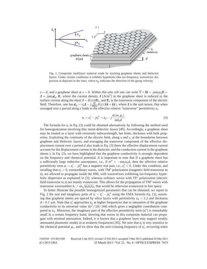
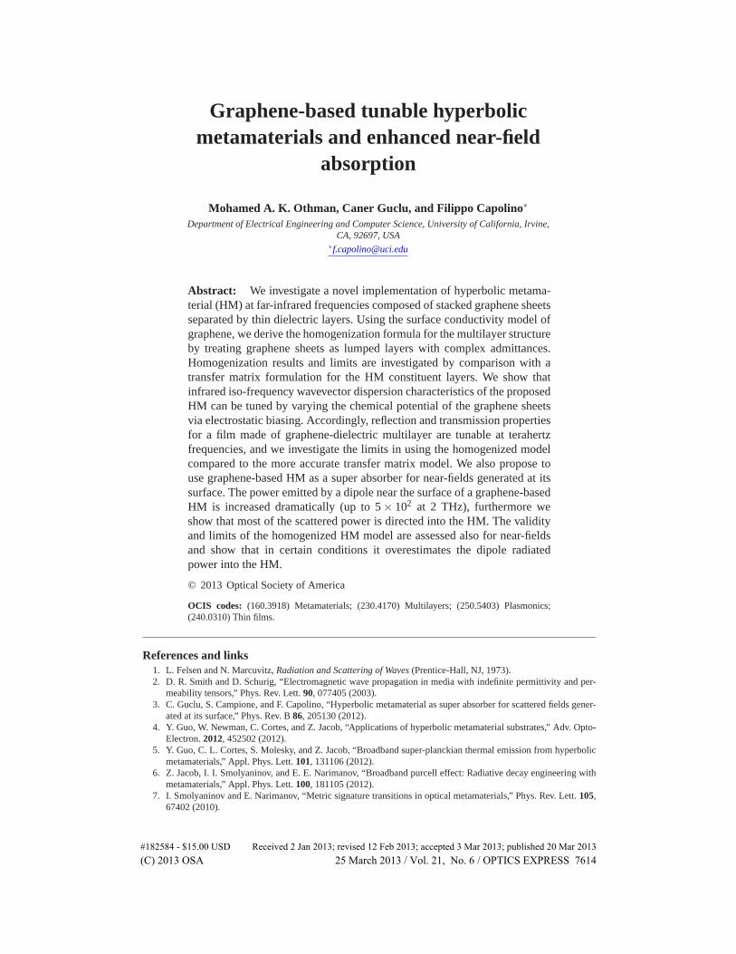
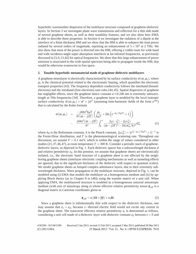
Fig. 1. Composite multilayer material made by stacking graphene sheets and dielectriclayers. Under certain conditions it exhibits hyperbolic-like iso-frequency wavevector dis-persion as depicted in the inset, where vg indicates the direction of the group velocity.
z = d, and a graphene sheet at z = 0. Within this unit cell one can write ∇×H = jωε0εdE+J = jωε0εεεd ·E, where the current density J [A/m2] in the graphene sheet is reduced to thesurface current along the sheet J = δ (z)σEt , and Et is the transverse component of the electricfield. Therefore, one has εεεd = εdI− j σ
ωε0δ (z)(xx+ yy), where I is the unit tensor, that when
averaged over a period along z leads to the effective relative “transverse” permittivity εt ,
εt = ε ′t − jε ′′t = εd − jσ(ω,μc)
ωε0d. (3)
The formula for εt in Eq. (3) could be obtained alternatively by following the method usedfor homogenization involving thin metal-dielectric layers [49]. Accordingly, a graphene sheetmay be treated as a layer with extremely subwavelength, but finite, thickness with bulk prop-erties. Exploiting the continuity of the electric field, along x and y, at the boundaries betweengraphene and dielectric layers, and averaging the transverse component of the effective dis-placement current over a period d also leads to Eq. (3) (here the effective displacement currentaccount for the displacement current in the dielectric and the conduction current in the graphenesheets ). In Eq. (3), we have highlighted that the graphene conductivity is strongly dependenton the frequency and chemical potential. It is important to note that if a graphene sheet hasa sufficiently large inductive susceptance, i.e., if σ ′′ < −ωε0εdd, then the effective relativepermittivity term εt = ε ′t − jε ′′t has a negative real part, i.e., ε ′t < 0. Under this condition, andrecalling that εz > 0, extraordinary waves, with TMz polarization (magnetic field transverse toz), are allowed to propagate inside the HM, with wavevectors exhibiting iso-frequency hyper-bolic dispersion as explained in [3]; whereas ordinary waves with TEz polarization (electricfield transverse to z) are mainly evanescent. This allows for the propagation of TMz waves withtransverse wavenumber kt > ω√μ0ε0εd , that would be otherwise evanescent in free space.
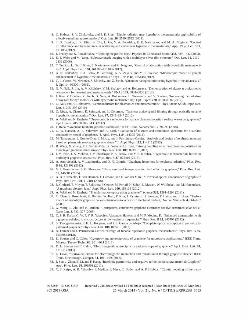
To better illustrate the possible homogenized parameters that can be obtained, we report inFig. 2 the real and imaginary parts of εt = ε ′t − jε ′′t using the EMA formula Eq. (3), assum-ing that graphene sheets are spaced by silica layers with permittivity εd = 2.2 and thicknessd= 0.1 µm. Note that ε ′t approaches εd at higher frequencies due to saturation of the grapheneconductivity to its universal value πe2/(2h) [44] which gives a negligible contribution com-pared to εd . Moreover, the imaginary part of the effective permittivity term (ε ′′t ) is remarkablysmall in a certain frequency band, showing that waves in this composite material can propa-gate with minimal attenuation. Indeed, it is known that a graphene layer may support weaklyattenuated plasmonic modes in at terahertz frequencies [45]. We note that εt is very sensitive tothe chemical potential μc, and we show that the zero-crossing frequency of ε ′t , occurring when
#182584 - $15.00 USD Received 2 Jan 2013; revised 12 Feb 2013; accepted 3 Mar 2013; published 20 Mar 2013(C) 2013 OSA 25 March 2013 / Vol. 21, No. 6 / OPTICS EXPRESS 7619
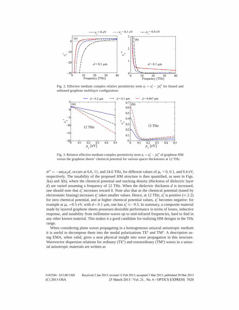
Fig. 2. Effective medium complex relative permittivity term εt = ε ′t − jε ′′t for biased andunbiased graphene multilayer configuration.
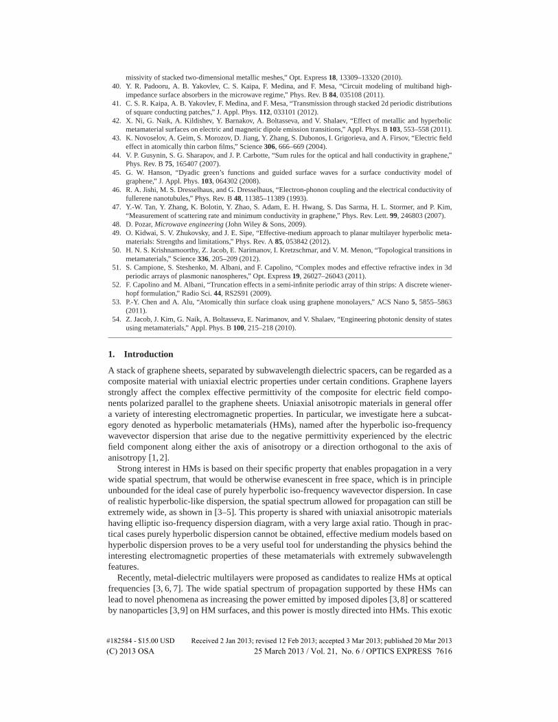
Fig. 3. Relative effective medium complex permittivity term εt = ε ′t − jε ′′t of graphene HMversus the graphene sheets’ chemical potential for various spacer thicknesses at 12 THz.
σ ′′ =−ωε0εdd, occurs at 6.6, 11, and 24.6 THz, for different values of μc = 0, 0.1, and 0.4 eV,respectively. The tunability of the proposed HM structure is then quantified, as seen in Figs.3(a) and 3(b), where the chemical potential and stacking density (thickness of dielectric layerd) are varied assuming a frequency of 12 THz. When the dielectric thickness d is increased,one should note that ε ′t increases toward 0. Note also that as the chemical potential (tuned byelectrostatic biasing) increases ε ′t takes smaller values. Hence, at 12 THz, ε ′t is positive (≈ 2.2)for zero chemical potential, and at higher chemical potential values, ε ′t becomes negative: forexample at μc =0.5 eV, with d= 0.1 µm, one has ε ′t ≈−9.5. In summary, a composite materialmade by layered graphene sheets possesses desirable performance in terms of losses, inductiveresponse, and tunability from millimeter-waves up to mid-infrared frequencies, hard to find inany other known material. This makes it a good candidate for realizing HM designs in the THzrange.
When considering plane waves propagating in a homogeneous uniaxial anisotropic mediumit is useful to decompose them into the modal polarizations TEz and TMz. A description us-ing EMA, when valid, gives a neat physical insight into wave propagation in this structure.Wavevector dispersion relations for ordinary (TEz) and extraordinary (TMz) waves in a uniax-ial anisotropic materials are written as
#182584 - $15.00 USD Received 2 Jan 2013; revised 12 Feb 2013; accepted 3 Mar 2013; published 20 Mar 2013(C) 2013 OSA 25 March 2013 / Vol. 21, No. 6 / OPTICS EXPRESS 7620
k2z + k2
t = εt k20, TEz (4)
k2z
εt+
k2t
εz= k2
0, TMz (5)
where k0 = ω√μ0ε0 is the wavenumber in vacuum, and we use kt =√
k2x + k2
y thanks to sym-
metry about the z axis. It is apparent that TMz waves in a medium with εt < 0 exhibit an iso-frequency wavenumber dispersion with hyperbolic shape, as explained in [3,5,50]. This allowsthe propagation of the extraordinary waves (TMz) with any transverse wavenumber kt >
√εdk0,
that would be otherwise evanescent in a homogeneous dielectric with permittivity εd . However,one should note that TEz waves are mainly evanescent when εt < 0, for any kt . The proposedgraphene-dielectric metamaterial can be used for realizing hyperbolic dispersion with εt < 0and εz > 0, and with the present implementation it is not possible to have anisotropy such thatεt > 0 and εz < 0. Elliptic dispersion regime occurring when both εt > 0 and εz > 0, inher-ently implies a propagating spectrum with kt <
√εzk0. Considering the multilayered structuredepicted in Fig. 1, we shall consider the root of k2
z , solution of Eq. (5), that corresponds to awave whose Poynting vector is directed toward the graphene-based HM, i.e, in the −z direc-tion, as shown with vg in Fig. 1. We assume here that the z-directed wavenumber may assumecomplex values, i.e., kz = βz − jαz, since the graphene conductivity σ is complex, modelingthe inhomogeneous plane wave spectrum. Accordingly, a wave that carries power in the −zdirection shall have the attenuation constant (αz) with negative sign, associated to field decay(due to possible losses) along the −z direction. In general βz can have both signs, though inour case it is positive, implying that the TMz mode is a backward wave for kt >
√εdk0, since
βzαz < 0 [51, 52].With the aim of assessing the validity of EMA in Eq. (4), we calculate the iso-frequency
wavevector dispersion with the more accurate Bloch theory for the periodic structures. Thisis done by treating each graphene layer as a complex lumped admittance Ys = σ (where thesubscript “s” denotes surface) as a shunt load in a transverse equivalent network (TEN, seeChapters 2 and 3 in [1]). This leads to the dispersion relation as (see Appendix A for moredetails)
cos(kzd) = cos(κdd)+ j12
σZd sin(κdd), (6)
where κd =√
εdk20 − k2
t is the z-directed wavenumber of a wave inside the dielectric, ZTEd =
ωμ0/κd , and ZTMd = κd/(ωε0εd) are the characteristic wave impedances for TEz and TMz
waves, respectively. Here we report only the dispersion curves that belong to TMz modes forbrevity, since they are those exhibiting hyperbolic-like dispersion.. We report in Figs. 4(a)-4(b), and Figs. 4(c)-4(d) the plots of kz = βz − jαz versus kt , for TMz waves at 2 and 12 THz,respectively, by applying EMA Eq. (5) and Bloch theory Eq. (6), for the graphene-dielectic HM(with εd = 2.2 and d= 0.1 µm), for various chemical potentials μc. We plot only the dispersionbranch relative to power propagation in the downward direction (see Fig. 1). However oneshould note the ±kz symmetry in the solutions of Eq. (6). One can observe in Fig. 4 that EMAand Bloch theory are in very good agreement for a wide range of transverse wavenumber kt
showing a hyperbolic relation, whereas the curves obtained from the two methods diverge forlarge kt and the dispersion curve obtained via Bloch theory shows a switching to a mainlyevanescent spectrum after certain kt . This observation is in accordance with the simplificationof the dispersion relation obtained from Bloch theory as follows. Let us consider the specialbut important case with |κdd| � 1, and |kzd| � 1, i.e., the period d is subwavelength, withrespect to the wavenumber in the dielectric and with respect to the Bloch wavenumber (the
#182584 - $15.00 USD Received 2 Jan 2013; revised 12 Feb 2013; accepted 3 Mar 2013; published 20 Mar 2013(C) 2013 OSA 25 March 2013 / Vol. 21, No. 6 / OPTICS EXPRESS 7621
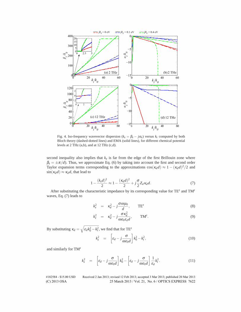
Fig. 4. Iso-frequency wavevector dispersion (kz = βz − jαz) versus kt computed by bothBloch theory (dashed-dotted lines) and EMA (solid lines), for different chemical potentiallevels at 2 THz (a,b), and at 12 THz (c,d).
second inequality also implies that kz is far from the edge of the first Brillouin zone whereβz = ±π/d). Thus, we approximate Eq. (6) by taking into account the first and second orderTaylor expansion terms corresponding to the approximations cos(κdd) ≈ 1− (κdd)2/2 andsin(κdd)≈ κdd, that lead to
1− (kzd)2
2≈ 1− (κdd)2
2+ j
σ2
Zdκdd. (7)
After substituting the characteristic impedance by its corresponding value for TEz and TMz
waves, Eq. (7) leads to
k2z = κ2
d − jσωμ0
d, TEz (8)
k2z = κ2
d − jσκ2
d
ωε0εdd, TMz. (9)
By substituting κd =√
εdk20 − k2
t , we find that for TEz
k2z =
[εd − j
σωε0d
]k2
0 − k2t , (10)
and similarly for TMz
k2z =
[εd − j
σωε0d
]k2
0 −[
εd − jσ
ωε0d
]1εd
k2t . (11)
#182584 - $15.00 USD Received 2 Jan 2013; revised 12 Feb 2013; accepted 3 Mar 2013; published 20 Mar 2013(C) 2013 OSA 25 March 2013 / Vol. 21, No. 6 / OPTICS EXPRESS 7622
Note that if one defines an effective transverse permittivity as in Eq. (3), the wavenumber dis-persions, just found above, become
k2z = εt k
20 − k2
t , TEz (12)
k2z = εt k
20 −
εt
εzk2
t , TMz (13)
which are identical to the wavevector dispersion relations provided in Eqs. (4) and (5) usingEMA.
It is clear from the analytical analysis above and from Fig. 4 that EMA well describes thewavevector dispersion when |κdd|� 1 and |kzd|� 1, which can be verified when the transversewavenumber kt is not too large. For larger and larger values of kt , the two assumptions would notbe valid anymore. In Fig. 4, we also report the evolution of the dispersion curves by varying thechemical potential μc at 2 THz and 12 THz. For example at 2 THz, when μc = 0.4 eV, the spatialspectrum is bounded by kt ≈ 36k0 after which αz increases dramatically. However, by increasingthe chemical potential, ε ′t assumes larger negative values and βz−kt dispersion in Fig. 4 evolvesto a flatter curve, thus the Brillouin zone edge is reached at larger values of kt . Note that at largerspatial spectrum, the attenuation constant αz increases due to finite losses, as shown in Fig. 4(b).By tuning the chemical potential, the dispersion characteristics can be controlled, for example,at 12 THz the dispersion for unbiased graphene is elliptic as well as when μc = 0.1 eV. Thisbehavior appears since ε ′t exhibits zero crossing and becomes positive at 6.6 THz and 11 THz,when μc = 0 and μc = 0.1 eV, respectively. However, when the chemical potential is increasedto 0.4 eV, hyperbolic dispersion arises at 12 THz, as shown in Figs. 4(c) and 4(d) where theinset of Fig. 4(c) shows the elliptic behavior for kt <
√εdk0. At high frequencies where the
conductivity saturates to its universal value, the TMz plasmonic modes are extremely confinedto graphene layers (σ ′′ becomes very small) and higher frequencies, once σ ′′ > 0, graphenelayers are incapable of supporting those modes [21]. Hence, the spectrum kt >
√εdk0 becomes
mainly evanescent at frequencies with ε ′t > 0. In other words, after ε ′t exhibits a zero-crossingand becomes positive, the wavevector dispersion becomes elliptic.
3. Plane wave reflection and transmission by a thin film made of graphene-dielectricmultilayers
A finite thickness graphene-dielectric multilayer film is considered comprising N graphenesheets stacked with silica SiO2 dielectric spacer, such that a graphene sheet is at the topmostlayer. The thickness of each SiO2 spacer is 0.1 µm, and the total multilayered film thicknessis D = Nd. For simplicity, all graphene layers are biased equally using a constant electrostaticpotential [34]. For practical consideration, suppose that a thin film of silica (in the order of100 nm) is deposited on an epitaxially-grown graphene monolayer repeatedly until creatingan N layer stack; though larger thicknesses could be considered, it is rather simple to achievethe biasing range (μc up to 0.5 eV) using relatively lower electrostatic potential for smallerthicknesses [34, 53].
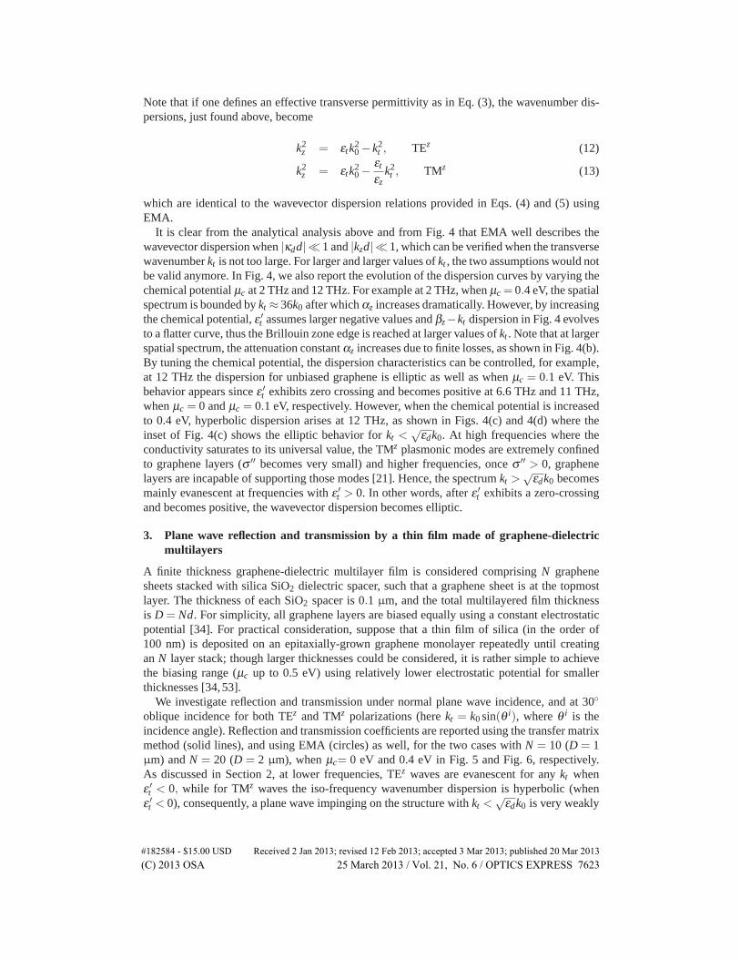
We investigate reflection and transmission under normal plane wave incidence, and at 30◦oblique incidence for both TEz and TMz polarizations (here kt = k0 sin(θ i), where θ i is theincidence angle). Reflection and transmission coefficients are reported using the transfer matrixmethod (solid lines), and using EMA (circles) as well, for the two cases with N = 10 (D = 1µm) and N = 20 (D = 2 µm), when μc= 0 eV and 0.4 eV in Fig. 5 and Fig. 6, respectively.As discussed in Section 2, at lower frequencies, TEz waves are evanescent for any kt whenε ′t < 0, while for TMz waves the iso-frequency wavenumber dispersion is hyperbolic (whenε ′t < 0), consequently, a plane wave impinging on the structure with kt <
√εdk0 is very weakly
#182584 - $15.00 USD Received 2 Jan 2013; revised 12 Feb 2013; accepted 3 Mar 2013; published 20 Mar 2013(C) 2013 OSA 25 March 2013 / Vol. 21, No. 6 / OPTICS EXPRESS 7623
° °
Fig. 5. Reflection and transmission versus frequency for a finite thickness graphene-silicamultilayered HM, at normal, and oblique incidence for both TEz and TMz polarizations,calculated by transfer matrix method (solid lines) and EMA (circles) when graphene layersare unbiased, i.e., μc = 0 eV.
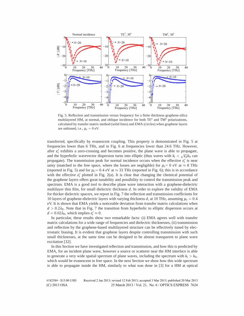
transferred, specifically by evanescent coupling. This property is demonstrated in Fig. 5 atfrequencies lower than 6 THz, and in Fig. 6 at frequencies lower than 24.6 THz. However,after ε ′t exhibits a zero-crossing and becomes positive, the plane wave is able to propagate,and the hyperbolic wavevector dispersion turns into elliptic (thus waves with kt <
√εdk0 can
propagate). The transmission peak for normal incidence occurs when the effective ε ′t is nearunity (matched to the free space, where the losses are negligible) for μc= 0 eV at ≈ 8 THz(reported in Fig. 5) and for μc= 0.4 eV at ≈ 33 THz (reported in Fig. 6); this is in accordancewith the effective ε ′t plotted in Fig. 2(a). It is clear that changing the chemical potential ofthe graphene layers offers great tunability and possibility to control the transmission peak andspectrum. EMA is a good tool to describe plane wave interaction with a graphene-dielectricmultilayer thin film, for small dielectric thickness d. In order to explore the validity of EMAfor thicker dielectric spacers, we report in Fig. 7 the reflection and transmission coefficients for10 layers of graphene-dielectric layers with varying thickness d, at 10 THz, assuming μc = 0.4eV. It is shown that EMA yields a noticeable deviation from transfer matrix calculations whend > 0.2λ0. Note that in Fig. 7 the transition from hyperbolic to elliptic dispersion occurs atd = 0.02λ0, which implies ε ′t ≈ 0.
In particular, these results show two remarkable facts: (i) EMA agrees well with transfermatrix calculations for a wide range of frequencies and dielectric thicknesses, (ii) transmissionand reflection by the graphene-based multilayered structure can be effectively tuned by elec-trostatic biasing. It is evident that graphene layers despite controlling transmission with suchsmall thicknesses, at the same time can be designed to be almost transparent to plane waveexcitation [32].
In this Section we have investigated reflection and transmission, and how this is predicted byEMA, for an incident plane wave, however a source or scatterer near the HM interface is ableto generate a very wide spatial spectrum of plane waves, including the spectrum with kt > k0,which would be evanescent in free space. In the next Section we show how this wide spectrumis able to propagate inside the HM, similarly to what was done in [3] for a HM at optical
#182584 - $15.00 USD Received 2 Jan 2013; revised 12 Feb 2013; accepted 3 Mar 2013; published 20 Mar 2013(C) 2013 OSA 25 March 2013 / Vol. 21, No. 6 / OPTICS EXPRESS 7624
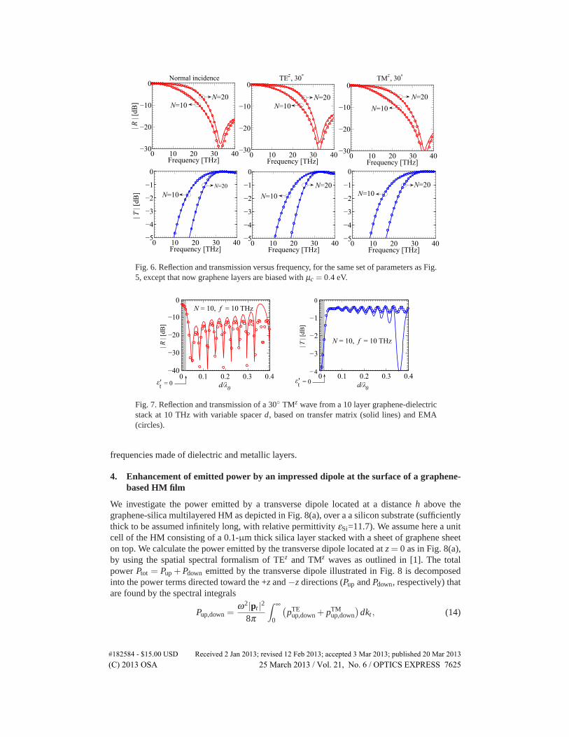
Fig. 6. Reflection and transmission versus frequency, for the same set of parameters as Fig.5, except that now graphene layers are biased with μc = 0.4 eV.
Fig. 7. Reflection and transmission of a 30◦ TMz wave from a 10 layer graphene-dielectricstack at 10 THz with variable spacer d, based on transfer matrix (solid lines) and EMA(circles).
frequencies made of dielectric and metallic layers.
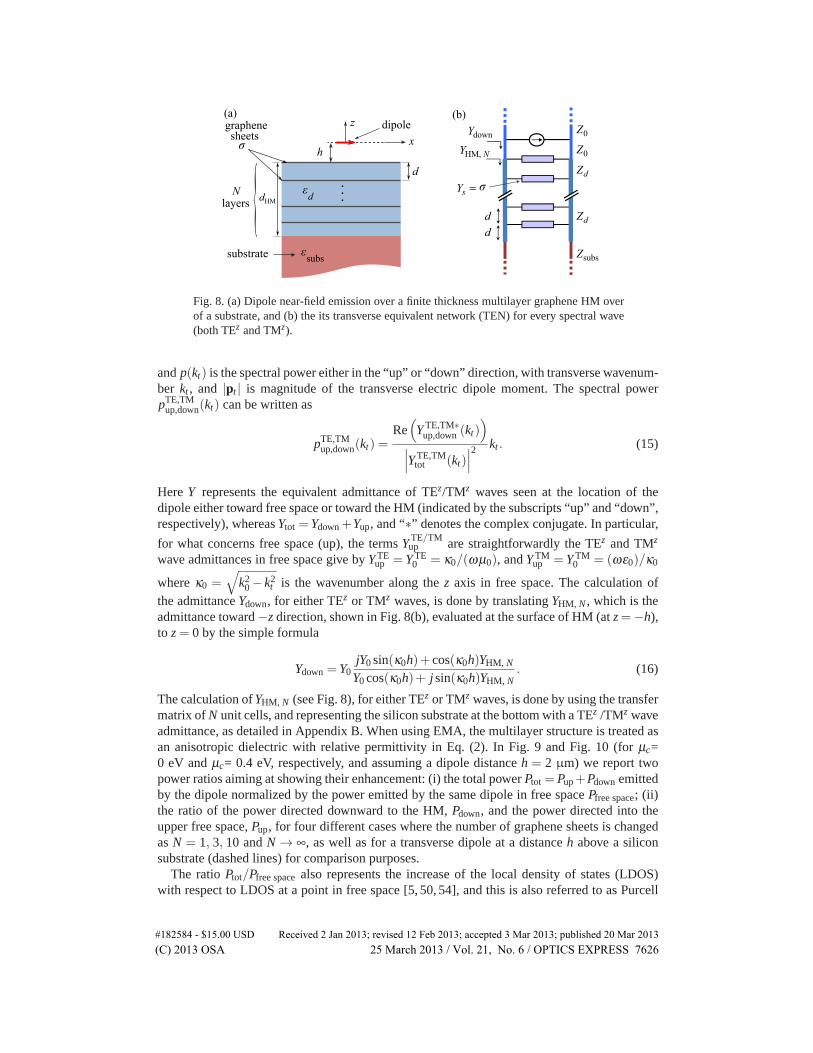
4. Enhancement of emitted power by an impressed dipole at the surface of a graphene-based HM film
We investigate the power emitted by a transverse dipole located at a distance h above thegraphene-silica multilayered HM as depicted in Fig. 8(a), over a a silicon substrate (sufficientlythick to be assumed infinitely long, with relative permittivity εSi=11.7). We assume here a unitcell of the HM consisting of a 0.1-µm thick silica layer stacked with a sheet of graphene sheeton top. We calculate the power emitted by the transverse dipole located at z = 0 as in Fig. 8(a),by using the spatial spectral formalism of TEz and TMz waves as outlined in [1]. The totalpower Ptot = Pup +Pdown emitted by the transverse dipole illustrated in Fig. 8 is decomposedinto the power terms directed toward the +z and −z directions (Pup and Pdown, respectively) thatare found by the spectral integrals
Pup,down =ω2|pt |2
8π
∫ ∞
0
(pTE
up,down + pTMup,down
)dkt , (14)
#182584 - $15.00 USD Received 2 Jan 2013; revised 12 Feb 2013; accepted 3 Mar 2013; published 20 Mar 2013(C) 2013 OSA 25 March 2013 / Vol. 21, No. 6 / OPTICS EXPRESS 7625
=
Fig. 8. (a) Dipole near-field emission over a finite thickness multilayer graphene HM overof a substrate, and (b) the its transverse equivalent network (TEN) for every spectral wave(both TEz and TMz).
and p(kt) is the spectral power either in the “up” or “down” direction, with transverse wavenum-ber kt , and |pt | is magnitude of the transverse electric dipole moment. The spectral powerpTE,TM
up,down(kt) can be written as
pTE,TMup,down(kt) =
Re(Y TE,TM∗
up,down (kt))
∣∣∣Y TE,TMtot (kt)
∣∣∣2kt . (15)
Here Y represents the equivalent admittance of TEz/TMz waves seen at the location of thedipole either toward free space or toward the HM (indicated by the subscripts “up” and “down”,respectively), whereas Ytot =Ydown +Yup, and “∗” denotes the complex conjugate. In particular,
for what concerns free space (up), the terms Y TE/TMup are straightforwardly the TEz and TMz
wave admittances in free space give by YTEup = Y TE
0 = κ0/(ωμ0), and Y TMup = Y TM
0 = (ωε0)/κ0
where κ0 =√
k20 − k2
t is the wavenumber along the z axis in free space. The calculation ofthe admittance Ydown, for either TEz or TMz waves, is done by translating YHM, N , which is theadmittance toward −z direction, shown in Fig. 8(b), evaluated at the surface of HM (at z =−h),to z = 0 by the simple formula
Ydown = Y0jY0 sin(κ0h)+ cos(κ0h)YHM, N
Y0 cos(κ0h)+ j sin(κ0h)YHM, N. (16)
The calculation of YHM, N (see Fig. 8), for either TEz or TMz waves, is done by using the transfermatrix of N unit cells, and representing the silicon substrate at the bottom with a TEz /TMz waveadmittance, as detailed in Appendix B. When using EMA, the multilayer structure is treated asan anisotropic dielectric with relative permittivity in Eq. (2). In Fig. 9 and Fig. 10 (for μc=0 eV and μc= 0.4 eV, respectively, and assuming a dipole distance h = 2 µm) we report twopower ratios aiming at showing their enhancement: (i) the total power Ptot = Pup+Pdown emittedby the dipole normalized by the power emitted by the same dipole in free space Pfree space; (ii)the ratio of the power directed downward to the HM, Pdown, and the power directed into theupper free space, Pup, for four different cases where the number of graphene sheets is changedas N = 1, 3, 10 and N → ∞, as well as for a transverse dipole at a distance h above a siliconsubstrate (dashed lines) for comparison purposes.
The ratio Ptot/Pfree space also represents the increase of the local density of states (LDOS)with respect to LDOS at a point in free space [5, 50, 54], and this is also referred to as Purcell
#182584 - $15.00 USD Received 2 Jan 2013; revised 12 Feb 2013; accepted 3 Mar 2013; published 20 Mar 2013(C) 2013 OSA 25 March 2013 / Vol. 21, No. 6 / OPTICS EXPRESS 7626
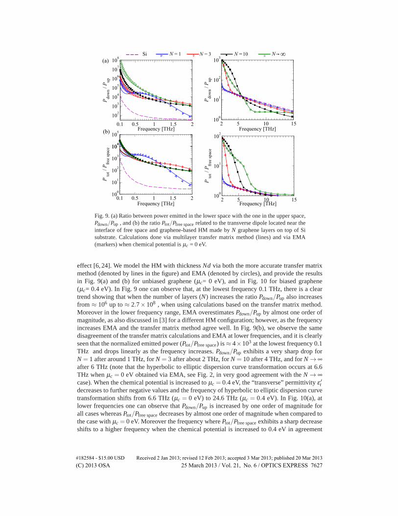
Fig. 9. (a) Ratio between power emitted in the lower space with the one in the upper space,Pdown/Pup , and (b) the ratio Ptot/Pfree space related to the transverse dipole located near theinterface of free space and graphene-based HM made by N graphene layers on top of Sisubstrate. Calculations done via multilayer transfer matrix method (lines) and via EMA(markers) when chemical potential is μc = 0 eV.
effect [6, 24]. We model the HM with thickness Nd via both the more accurate transfer matrixmethod (denoted by lines in the figure) and EMA (denoted by circles), and provide the resultsin Fig. 9(a) and (b) for unbiased graphene (μc= 0 eV), and in Fig. 10 for biased graphene(μc= 0.4 eV). In Fig. 9 one can observe that, at the lowest frequency 0.1 THz, there is a cleartrend showing that when the number of layers (N) increases the ratio Pdown/Pup also increasesfrom ≈ 106 up to ≈ 2.7× 10⁸ , when using calculations based on the transfer matrix method.Moreover in the lower frequency range, EMA overestimates Pdown/Pup by almost one order ofmagnitude, as also discussed in [3] for a different HM configuration; however, as the frequencyincreases EMA and the transfer matrix method agree well. In Fig. 9(b), we observe the samedisagreement of the transfer matrix calculations and EMA at lower frequencies, and it is clearlyseen that the normalized emitted power (Ptot/Pfree space) is ≈ 4×10³ at the lowest frequency 0.1THz and drops linearly as the frequency increases. Pdown/Pup exhibits a very sharp drop forN = 1 after around 1 THz, for N = 3 after about 2 THz, for N = 10 after 4 THz, and for N → ∞after 6 THz (note that the hyperbolic to elliptic dispersion curve transformation occurs at 6.6THz when μc = 0 eV obtained via EMA, see Fig. 2, in very good agreement with the N → ∞case). When the chemical potential is increased to μc = 0.4 eV, the “transverse” permittivity ε ′tdecreases to further negative values and the frequency of hyperbolic to elliptic dispersion curvetransformation shifts from 6.6 THz (μc = 0 eV) to 24.6 THz (μc = 0.4 eV). In Fig. 10(a), atlower frequencies one can observe that Pdown/Pup is increased by one order of magnitude forall cases whereas Ptot/Pfree space decreases by almost one order of magnitude when compared tothe case with μc = 0 eV. Moreover the frequency where Ptot/Pfree space exhibits a sharp decreaseshifts to a higher frequency when the chemical potential is increased to 0.4 eV in agreement
#182584 - $15.00 USD Received 2 Jan 2013; revised 12 Feb 2013; accepted 3 Mar 2013; published 20 Mar 2013(C) 2013 OSA 25 March 2013 / Vol. 21, No. 6 / OPTICS EXPRESS 7627
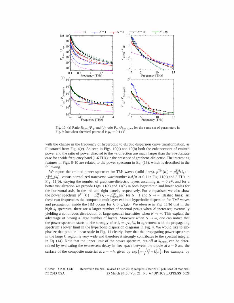
Fig. 10. (a) Ratio Pdown/Pup and (b) ratio Ptot/Pfree space for the same set of parameters inFig. 9, but when chemical potential is μc = 0.4 eV.
with the change in the frequency of hyperbolic to elliptic dispersion curve transformation, asillustrated from Fig. 4(c). As seen in Figs. 10(a) and 10(b) both the enhancement of emittedpower and the ratio of power directed to the –z direction are much larger than the Si-substratecase for a wide frequency band (1-6 THz) in the presence of graphene-dielectric. The interestingfeatures in Figs. 9-10 are related to the power spectrum in Eq. (15), which is described in thefollowing.
We report the emitted power spectrum for TMz waves (solid lines), pTM(kt) = pTMup (kt)+
pTMdown(kt), versus normalized transverse wavenumber ktd/π at 0.1 in Fig. 11(a) and 3 THz in
Fig. 11(b), varying the number of graphene-dielectric layers assuming μc = 0 eV, and for abetter visualization we provide Figs. 11(a) and 11(b) in both logarithmic and linear scales forthe horizontal axis, in the left and right panels, respectively. For comparison we also showthe power spectrum pTE(kt) = pTE
up (kt) + pTEdown(kt) for N =1 and N → ∞ (dashed lines). At
these two frequencies the composite multilayer exhibits hyperbolic dispersion for TMz wavesand propagation inside the HM occurs for kt >
√εdk0. We observe in Fig. 11(b) that in the
high kt spectrum, there are a larger number of spectral peaks when N increases; eventuallyyielding a continuous distribution of large spectral intensities when N → ∞. This explain theadvantage of having a large number of layers. Moreover when N → ∞, one can notice thatthe power spectrum starts to rise strongly after kt =
√εdk0, in agreement with the propagating
spectrum’s lower limit in the hyperbolic dispersion diagrams in Fig. 4. We would like to em-phasize that plots in linear scale in Fig. 11 clearly show that the propagating power spectrumin the large kt region is very wide and therefore it strongly contributes to the spectral integralin Eq. (14). Note that the upper limit of the power spectrum, cut-off at kt,max, can be deter-mined by evaluating the evanescent decay in free space between the dipole at z = 0 and the
surface of the composite material at z = −h, given by exp(−√
k2t − k2
0h)
. For example, by
#182584 - $15.00 USD Received 2 Jan 2013; revised 12 Feb 2013; accepted 3 Mar 2013; published 20 Mar 2013(C) 2013 OSA 25 March 2013 / Vol. 21, No. 6 / OPTICS EXPRESS 7628
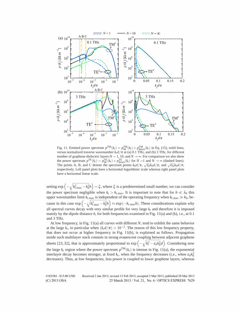
Fig. 11. Emitted power spectrum pTM(kt) = pTMup (kt)+ pTM
down(kt) in Eq. (15), solid lines,versus normalized traverse wavenumber ktd/π at (a) 0.1 THz, and (b) 3 THz, for differentnumber of graphene-dielectric layers:N = 1, 10, and N → ∞. For comparison we also showthe power spectrum pTE(kt) = pTE
up (kt)+ pTEdown(kt) for N =1 and N → ∞ (dashed lines).
The points A, B, and C denote the spectrum points k0d/π ,√εdk0d/π , and
√εSik0d/π ,
respectively. Left panel plots have a horizontal logarithmic scale whereas right panel plotshave a horizontal linear scale.
setting exp(−√
k2t,max − k2
0h)= ξ , where ξ is a predetermined small number, we can consider
the power spectrum negligible when kt > kt,max. It is important to note that for h � λ0 thisupper wavenumber limit kt,max is independent of the operating frequency when kt,max k0, be-
cause in this case exp(−√
k2t,max − k2
0h)≈ exp(−kt,maxh). These considerations explain why
all spectral curves decay with very similar profile for very large kt and therefore it is imposedmainly by the dipole distance h, for both frequencies examined in Fig. 11(a) and (b), i.e., at 0.1and 3 THz.
At low frequency, in Fig. 11(a) all curves with different N, tend to exhibit the same behaviorat the large kt , in particular when (ktd/π) > 10−2. The reason of this low frequency property,that does not occur at higher frequency in Fig. 11(b), is explained as follows. Propagationinside such multilayer stack consists in strong evanescent coupling between adjacent graphene
sheets [23, 32], that is approximately proportional to exp(−√
k2t − εdk2
0d)
. Considering now
the large kt region where the power spectrum pTM(kt) is intense in Fig. 11(a), the exponentialinterlayer decay becomes stronger, at fixed kt , when the frequency decreases (i.e., when εdk2
0decreases). Thus, at low frequencies, less power is coupled to lower graphene layers, whereas
#182584 - $15.00 USD Received 2 Jan 2013; revised 12 Feb 2013; accepted 3 Mar 2013; published 20 Mar 2013(C) 2013 OSA 25 March 2013 / Vol. 21, No. 6 / OPTICS EXPRESS 7629
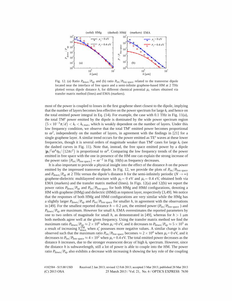
Fig. 12. (a) Ratio Pdown/Pup and (b) ratio Ptot/Pfree space related to the transverse dipolelocated near the interface of free space and a semi-infinite graphene-based HM at 2 THzplotted versus dipole distance h, for different chemical potential μc values obtained viatransfer matrix method (lines) and EMA (markers).
most of the power is coupled to losses in the first graphene sheet closest to the dipole, implyingthat the number of layers becomes less effective on the power spectrum for large kt and hence onthe total emitted power integral in Eq. (14). For example, the case with 0.1 THz in Fig. 11(a),the total TMz power emitted by the dipole is dominated by the wide power spectrum region(5×10⁻³π/d
)< kt < kt,max, which is weakly dependent on the number of layers. Under this
low frequency condition, we observe that the total TMz emitted power becomes proportionalto ω2, independently on the number of layers, in agreement with the findings in [21] for asingle graphene layer. A similar trend occurs for the power emitted as TEz waves at these lowerfrequencies, though it is several orders of magnitude weaker than TMz cases for large kt (seethe dashed curves in Fig. 11). Note that, instead, the free space emitted power by a dipole|pt |2ω4η0/
(12πc2
)is proportional to ω4. Comparing the low frequency trends of the power
emitted in free space with the one in presence of the HM one can explain the strong increase ofthe power ratio
(Ptot/Pfree space
)∝ ω−2 in Fig. 10(b) as frequency decreases.
It is also important to provide a physical insight into the effect of the distance h on the poweremitted by the impressed transverse dipole. In Fig. 12, we provide the plots of Ptot/Pfree space
and Pdown/Pup at 2 THz versus the dipole’s distance h for the semi-infinitely periodic (N → ∞)graphene-dielectric multilayered structure with μc= 0 eV and μc= 0.4 eV, obtained both viaEMA (markers) and the transfer matrix method (lines). In Figs. 12(a) and 12(b) we report thepower ratios Pdown/Pup and Ptot/Pfree space for both HMg and HMd configurations, denoting aHM with graphene (HMg) and dielectric (HMd) as topmost layer, respectively [3,49]. We noticethat the responses of both HMg and HMd configurations are very similar while the HMg hasa slightly larger Pdown/Pup and Ptot/Pfree space for smaller h, in agreement with the observationsin [49]. For the smallest reported distance h = 0.2 µm, the emitted power (Ptot/Pfree space ) andPdown/Pup are maximum. However for small h, EMA overestimates the reported parameters byone to two orders of magnitude for small h, as demonstrated in [49], whereas for h > 1 µmboth methods agree well at the given frequency. Using the transfer matrix method we find themaximum ratio Pdown/Pup ≈ 2×10⁶ when μc=0 eV, and it decreases to Pdown/Pup ≈ 5×10⁵ asa result of increasing Y TM
down when ε ′t possesses more negative values. A similar change is alsoobserved such that the maximum ratio Ptot/Pfree space becomes ≈ 2×10⁴ when μc= 0 eV, and itdecreases to Ptot/Pfree space ≈ 4×10² when μc= 0.4 eV. The total emitted power decreases as thedistance h increases, due to the stronger evanescent decay of high kt spectrum. However, sincethe distance h is subwavelength, still a lot of power is able to couple into the HM. The powerratio Pdown/Pup also exhibits a decrease with increasing h showing the key role of the coupling
#182584 - $15.00 USD Received 2 Jan 2013; revised 12 Feb 2013; accepted 3 Mar 2013; published 20 Mar 2013(C) 2013 OSA 25 March 2013 / Vol. 21, No. 6 / OPTICS EXPRESS 7630
of the evanescent spectrum in free space to the propagating spectrum in the HM. We finallynote from the observations in Fig. 12 that the accuracy of EMA is influenced by changing thevalues of μc, implying the effect of εt on EMA’s validity.
In summary, we have shown that the power emitted by a dipolar source in the proximity ofa graphene-based HM is strongly enhanced, and that it can be effectively tuned by electrostat-ically biasing the graphene sheets, which makes this HM a promising candidate for tunableapplications in the far-infrared frequencies.
5. Conclusion
We have investigated a novel design of HM for far-infrared frequencies based on graphenelayers. The multilayer structure has been analyzed using EMA which, based on a permittivityhomogenization model, predicts the HM features at far-infrared frequencies. We have quantita-tively shown the capability of tuning the composite material properties via chemical potential ofgraphene. We have investigated plane wave interaction with a thin film made by few graphenesheets, and showed how the transmission frequency spectrum can be tuned. We have assessedthe validity of EMA for both plane wave incidence and near-field radiation from a dipole, andwe have shown that under certain conditions EMA is in good agreement with the transfer matrixanalysis. In the last part of the paper, we have shown that a very wide spatial spectrum emittedby an electric dipole is allowed to couple into the graphene-based HM, that would be otherwiseevanescent in free space. This generates two interesting main features: (1) the power emittedby the dipole is strongly enhanced (up to several orders of magnitude) by the presence of thegraphene-based HM, and (2) most of the power is directed into the HM, also for relative sub-wavelength HM thicknesses realized with only a few graphene sheets.These properties seem toenable the use of this tunable graphene-based HM to efficiently absorb mm-waves and terahertzfrequencies, and give rise to other possible applications including super resolution lenses.
Acknowledgment
We thank the anonymous reviewers for their useful comments. We also would like to thankSalvatore Campione (University of California, Irvine) for fruitful discussions.
6. Appendix A
The transfer matrix [Tunit] of a unit cell composed of a graphene sheet (modeled as a lumpedshunt complex admittance Ys = σ ) and a dielectric layer of thickness d (modeled as a transmis-sion line) for TEz/TMz waves can be written as (assuming time-harmonic fields of the forme jωt )
[Tunit] =
[Aunit Bunit
Cunit Dunit
]=
[1 0σ 1
][ cos(κdd) jZd sin(κdd)j
Zdsin(κdd) cos(κdd)
]
=
[cos(κdd) jZd sin(κdd)
jZd
sin(κdd)+σ cos(κdd) jσZd sin(κdd)+ cos(κdd)
], (17)
where κd =√
εdk20 − k2
t is wavenumber along the z axis inside the dielectric, and for TEz and
TMz waves: ZTEd = ωμ0/κd and ZTM
d = κd/(ωε0εd), respectively. We are interested in deter-mining the Bloch wavenumber kz in the z-direction, that describes layer to layer propagation.Following the simple procedure in [48], the wavevector dispersion relation can be obtainedfrom the solution of the eigenvalue problem
∣∣[Tunit]− e− jkzd [I]∣∣ = 0, where [I] is the identity
matrix. This leads to the simple dispersion relation in Eq. (6).
#182584 - $15.00 USD Received 2 Jan 2013; revised 12 Feb 2013; accepted 3 Mar 2013; published 20 Mar 2013(C) 2013 OSA 25 March 2013 / Vol. 21, No. 6 / OPTICS EXPRESS 7631
7. Appendix B
The calculation of the admittance looking toward the −z direction YHM, N (see Fig. 8) can bestraightforwardly carried out by constructing the transfer matrix of the HM film made of N unitcells [TN ], between the bottom-most material, i.e., the silicon substrate at z = −(Nd + h), andthe surface of HM at z = −h. By knowing the transfer matrix of the unit cell [Tunit], given inEq. (17), one has
[TN ] =
[AN BN
CN DN
]= [Tunit]
N . (18)
Then YHM, N is evaluated using the entries of the transfer matrix [TN ] and the wave admittanceinside silicon substrate, Ysubs, as
YHM, N =CN +DNYsubs
AN +BNYsubs, (19)
where Y TEsubs = κsubs/(ωμ0) and Y TM
subs =ωε0εsubs/κsubs are the TEz and TMz wave impedances in
the substrate, κsubs =√
εsubsk20 − k2
t is the z-directed wavenumber, and εsubs = εSi is the relativepermittivity of silicon. When we consider the semi-infinite case, N → ∞, the admittance YHM, N
becomes the Bloch admittance YBloch of the periodic multilayer evaluated using the unit cell’stransfer matrix entries in Eq. (17) as
YBloch =Aunit −Dunit ±
√(Aunit +Dunit)2 −4
−2Bunit. (20)
Here one should pick the root of YBloch such that Re(YBloch)> 0, representing waves that carrypower in the −z direction.
#182584 - $15.00 USD Received 2 Jan 2013; revised 12 Feb 2013; accepted 3 Mar 2013; published 20 Mar 2013(C) 2013 OSA 25 March 2013 / Vol. 21, No. 6 / OPTICS EXPRESS 7632