gunasekhar aluru b - digital library/67531/metadc849770/m2/1/high...gunasekhar aluru b.e ......
TRANSCRIPT

EXPLORING ANALOG AND DIGITAL DESIGN USING THE
OPEN-SOURCE ELECTRIC VLSI DESIGN SYSTEM
Gunasekhar Aluru B.E
Thesis Prepared for the Degree of
MASTER OF SCIENCE
UNIVERSITY OF NORTH TEXAS
May 2016
APPROVED:
Saraju P. Mohanty, Major ProfessorElias Kougianos, Co-Major ProfessorPhilip H. Sweany, Committee MemberBarrett Bryant, Chair of the Department of
Computer Science and EngineeringCostas Tsatsoulis,
Dean of the College of EngineeringCostas Tsatsoulis, Dean of the Robert B. Toulouse
School of Graduate Studies

Aluru, Gunasekhar. Exploring Analog and Digital Design Using the Open-Source
Electric VLSI Design System. Master of Science (Computer Engineering), May 2016, 79
pp., 9 tables, 62 figures, references, 38 titles.
The design of VLSI electronic circuits can be achieved at many different abstraction
levels starting from system behavior to the most detailed, physical layout level. As the
number of transistors in VLSI circuits is increasing, the complexity of the design is also
increasing, and it is now beyond human ability to manage. Hence CAD (Computer Aided
design) or EDA (Electronic Design Automation) tools are involved in the design. EDA or
CAD tools automate the design, verification and testing of these VLSI circuits. In today’s
market, there are many EDA tools available. However, they are very expensive and require
high-performance platforms. One of the key challenges today is to select appropriate CAD or
EDA tools which are open-source for academic purposes. This thesis provides a detailed
examination of an open-source EDA tool called Electric VLSI Design system. An excellent
and efficient CAD tool useful for students and teachers to implement ideas by modifying the
source code, Electric fulfills these requirements. This thesis’ primary objective is to explain
the Electric software features and architecture and to provide various digital and analog
designs that are implemented by this software for educational purposes. Since the choice of an
EDA tool is based on the efficiency and functions that it can provide, this thesis explains all
the analysis and synthesis tools that electric provides and how efficient they are. Hence, this
thesis is of benefit for students and teachers that choose Electric as their open-source EDA
tool for educational purposes.

Copyright 2016
by
Gunasekhar Aluru
ii

ACKNOWLEDGMENTS
Foremost, I would like to express my deepest gratitude to my major professor, Dr.
Saraju P. Mohanty, for his continuous help during my Thesis work and research, for his
encouragement, motivation, enthusiasm, and immense knowledge. Words do not suffice to
show how thankful I am. I would like to extend my deepest appreciation to my co-major
professor, Dr. Elias Kougianos, for his encouragement, support, advice and feedback that
helped me through the completion of this work. I would also like to thank my committee
member Philip H. Sweany, for encouragement and providing insightful comments. I would
also like to extend my appreciation to the Deaprtment of Computer Science and Engineering
(http://www.cse.unt.edu), which provided me with useful resources that made my work
easy.
My special thanks to my father Gurubrahmam, my mother Padmavathi and brother
Jayasekhar. Without their support, love and patience none of this would be possible. Last
but no least, I would like to thank my fellow Nanosystem Design Laboratory (NSDL,
http://nsdl.cse.unt.edu) members and friends who supported me throughout this process.
iii

TABLE OF CONTENTS
Page
ACKNOWLEDGMENTS iii
LIST OF TABLES vii
LIST OF FIGURES viii
CHAPTER 1 INTRODUCTION 1
1.1. Existing Open-Source EDA Tools 2
1.2. Organization of the Thesis 3
CHAPTER 2 THE ELECTRIC VLSI DESIGN SYSTEM:
FEATURES AND SOFTWARE ARCHITECTURE 4
2.1. Electric History 4
2.2. Electric Installation 5
2.2.1. Downloading Electric 5
2.2.2. Supported Environments 6
2.2.3. System Requirements 6
2.2.4. Plugins 7
2.2.5. Source Code 7
2.3. Electric Features 10
2.3.1. Electric GUI 10
2.3.2. Representation 11
2.3.3. Design Environments 13
2.3.4. Analysis and Synthesis Tools 14
2.3.5. External Interfaces 22
iv

2.3.6. Parasitic Extraction 23
2.4. Design Flow in Electric 24
2.4.1. Schematic level Design 24
2.4.2. Physical level Design 24
2.5. Scripting in Electric 27
2.6. Electric Advantages 32
CHAPTER 3 DIGITAL INTEGRATED CIRCUIT DESIGN USING ELECTRIC 34
3.1. ALU 34
3.1.1. Gate level Components 34
3.1.2. Implementation of AN 8-bit ALU 42
3.2. 2-Bit Multiplier 44
3.2.1. Logic Level Components 46
3.2.2. Implementation of a 2-bit Multiplier 47
3.3. Frequency Divider 49
3.3.1. Logic level Compoenents 51
3.3.2. Implementation of Frequency divider 53
3.4. 1-Bit SRAM 54
3.4.1. 6T-Cell 56
3.4.2. Implemtation of a 1-bit SRAM 56
CHAPTER 4 ANALOG INTEGRATED CIRCUIT DESIGN USING ELECTRIC 60
4.1. 3-Stage Ring Oscillator 60
4.1.1. Schematic Design 61
4.1.2. Physical Design 62
4.1.3. Simulation Results 63
4.2. Voltage Controlled Oscillator 64
4.2.1. Schematic Design 64
4.2.2. Physical Design 65
v

4.2.3. Simulation results 66
4.3. Sense Amplifier 67
4.3.1. Schematic Design 67
4.3.2. Physical Design 69
4.3.3. Simulation Results 69
4.4. Charge Pump 71
4.4.1. Schematic Design 71
4.4.2. Physical Design 71
4.4.3. Simulation Results 72
CHAPTER 5 CONCLUSION AND FUTURE RESEARCH 74
5.1. Summary and Conclusions 74
5.2. Future Research 75
BIBLIOGRAPHY 76
vi

LIST OF TABLES
Page
Table 1.1. Existing Open Source EDA tools 3
Table 2.1. List of Fundamental Packages in the Electric source code. 9
Table 2.2. Design Environments in Electric. 15
Table 2.3. List of fundamental design rules. 19
Table 2.4. Important Methods for Designing in mocmos technology. 32
Table 3.1. Functions selected by 2-bit F inputs 45
Table 3.2. Input and output values for 8-bit ALU 45
Table 4.1. Ring Oscillator Characteristics 63
Table 4.2. Characteristics of the 180-nm TSMC CMOS VCO 67
vii
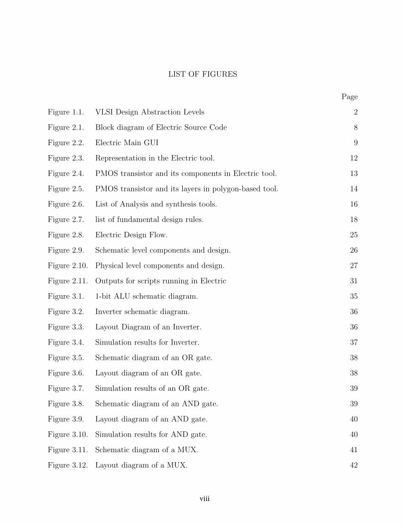
LIST OF FIGURES
Page
Figure 1.1. VLSI Design Abstraction Levels 2
Figure 2.1. Block diagram of Electric Source Code 8
Figure 2.2. Electric Main GUI 9
Figure 2.3. Representation in the Electric tool. 12
Figure 2.4. PMOS transistor and its components in Electric tool. 13
Figure 2.5. PMOS transistor and its layers in polygon-based tool. 14
Figure 2.6. List of Analysis and synthesis tools. 16
Figure 2.7. list of fundamental design rules. 18
Figure 2.8. Electric Design Flow. 25
Figure 2.9. Schematic level components and design. 26
Figure 2.10. Physical level components and design. 27
Figure 2.11. Outputs for scripts running in Electric 31
Figure 3.1. 1-bit ALU schematic diagram. 35
Figure 3.2. Inverter schematic diagram. 36
Figure 3.3. Layout Diagram of an Inverter. 36
Figure 3.4. Simulation results for Inverter. 37
Figure 3.5. Schematic diagram of an OR gate. 38
Figure 3.6. Layout diagram of an OR gate. 38
Figure 3.7. Simulation results of an OR gate. 39
Figure 3.8. Schematic diagram of an AND gate. 39
Figure 3.9. Layout diagram of an AND gate. 40
Figure 3.10. Simulation results for AND gate. 40
Figure 3.11. Schematic diagram of a MUX. 41
Figure 3.12. Layout diagram of a MUX. 42
viii

Figure 3.13. Schematic Diagram of a Full Adder. 43
Figure 3.14. Layout Diagram of a Full adder. 43
Figure 3.15. Simulation results for a Full adder 44
Figure 3.16. Simulation results for 8-bit ALU. 45
Figure 3.17. Layout Diagram of a Full adder. 46
Figure 3.18. Schematic diagram of a half-adder. 47
Figure 3.19. Layout diagram of a half-adder. 47
Figure 3.20. 2-bit multiplication process. 48
Figure 3.21. Schematic diagram of a 2-bit multiplier. 49
Figure 3.22. Layout diagram of a 2-bit multiplier. 49
Figure 3.23. Input signals for a 2-bit multiplier. 50
Figure 3.24. Output signals for a 2-bit multiplier. 50
Figure 3.25. Schematic diagram of a JK Flip-Flop. 52
Figure 3.26. Layout Diagram of a JK Flip-Flop. 52
Figure 3.27. Schematic Diagram of NAND gate. 53
Figure 3.28. Simulation results for NAND gate. 53
Figure 3.29. Layout Diagram of a NAND gate. 54
Figure 3.30. Schematic diagram of a Frequency divider. 55
Figure 3.31. Layout diagram of a Frequency divider. 55
Figure 3.32. Simulation result for Frequency divider. 55
Figure 3.33. Schmetic circuit of an SRAM cell. 56
Figure 3.34. Layout diagram of an SRAM cell. 57
Figure 3.35. Schematic diagram of an 1-bit SRAM. 58
Figure 3.36. Layout diagram of an 1-bit SRAM. 59
Figure 3.37. 1-Bit SRAM Timing Waveform. 59
Figure 4.1. Schematic diagram of 3-Stage Ring Oscillator 61
Figure 4.2. Layout Diagram of 3-Stage Ring Oscillator. 62
Figure 4.3. Simulation Result of a Ring Oscillator. 63
ix

Figure 4.4. Schematic diagram of a 5-stage VCO. 65
Figure 4.5. Layout Diagram of the a 5-Stage VCO. 66
Figure 4.6. Simulation results for 5 stage VCO. 66
Figure 4.7. Schematic diagram of sense amplifier. 68
Figure 4.8. Physical design of sense amplifier. 69
Figure 4.9. Sensing Waveform for sense amplifier. 70
Figure 4.10. Control Signals for sense amplifier. 70
Figure 4.11. Schematic diagram of a Charge Pump. 72
Figure 4.12. Simulation results for Charge Pump. 73
Figure 4.13. Physical design of charge pump. 73
x
CHAPTER 1
INTRODUCTION
Electronic systems play a crucial role in human life. Electronic systems ranging from
Integrated Circuits (ICs) to PCB (Printed Circuit Boards) are developed and produced by
EDA (Electronic Design Automation) tools. EDA is a collection of algorithms, methodolo-
gies, and tools which automate the design, verification and testing of electronic systems.
There are many commercial EDA tools, which are the industry standard and very expensive
to license such as Cadence, Mentor Graphics, Synopsys, etc. Free/Open-Source Software
(FOSS) EDA tools are the only effective way for students and teachers to learn and im-
plement their ideas by modifying the source code. The Electric VLSI Design System is a
sophisticated open-source CAD system which can handle a variety of technologies such as
CMOS and Bipolar from schematics to the layout. It has many generic analysis and synthesis
tools which can automate the design and reduce the time and work. It also supports most
popular interchange and manufacturing formats such as EDIF, VHDL, GDS, LEF/DEF, etc.
[6, 35, 19].
Figure 1.1 shows the various VLSI design abstraction levels [19, 20]. Hardware de-
signers use these VLSI design abstraction levels to ensure that all the sets of specifications
and primary goals such as power consumption, speed, etc. are met. With the given set of
specifications, the main objective at the system level is to define the partitions of the system
and their interfaces. The next step is to represent the subsystem’s behavior using high-level
programming languages. Through behavioral verification, we could know whether the model
has met the requirements or not. After the specifications are assured, the next step in the
design process is to define the design at Register Transfer Level (RTL) [23]. At RTL, the
timing and data transfers between simple functional units such as registers, full-adders, de-
coders, counters, etc. are described. At gate level, the design is a structure of gates, latches,
and flip-flops. In this level, the accurate area and delay are estimated [21]. In transistor or
circuit level, the design is implemented with transistors. Physical design plays a most vital
1

System Level
Gate Level
Register-Transfer Level
Transistor Level
Physical Level
Figure 1.1. VLSI Design Abstraction Levels
role in the design steps because it deals with the area, power and performance of the final
electronic system or circuit. It also completes the floorplanning, placement, and routing
for the design [37]. The designer can use the Electric software from gate level to physical
level design of an IC design flow. Since it does not have an inbuilt Verilog simulator, it
can’t simulate Verilog code, but it can build Verilog decks for simulation in different Verilog
simulators.
1.1. Existing Open-Source EDA Tools
Based on the VLSI design flow, a good EDA tool should support features such as
logical design, circuit schematics, layout generation, and also design rule check. In today’s
market, most VLSI CAD systems which support all these features are not FOSS, but there
are some open source tools which support some features individually. These are listed in
table 1.1 [19]. The main drawback of other open-source EDA tools is that they are not
2

as comprehensive as Electric. Even though some tools support some features the totality
of features is not integrated into one CAD system which is FOSS. Only the Electric CAD
system supports all desired features and is comprehensive [34].
Tools Version Licence Supported Platform Funtions
Electric Version 9.06 GPL Mac OS, Windows, Linux HDL to Layout, Mixed-Signal
Toped Toped 0.9.8 GPL Windows, Linux Circuit Layout, Mixed-Signal
gEDA version 1.8.2 GPL Linux, Mac OS X PCB Design, Schematics
Magic Magic 8.1 BSD Linux Circuit Layout, Mixed-Signal
eSim Version 1.0.0 GPL Windows, Linux PCB Design, Schematics
Xcircuit Version 3.9 GPL Windows, Unix Schematic Capture
Qucs Release 0.0.18 GPL Mac OS, Windows, Linux PCB Design, Schematics
Table 1.1. Existing Open Source EDA tools
1.2. Organization of the Thesis
This thesis is organized as follows.
Chapter 2 explains the history, architecture, features and also installation of the Electric
VLSI Design system. Design environments, analysis and synthesis tools and also external
interfaces that are provided by Electric are described here.
Chapter 3 presents four digital designs that are implemented with Electric. The accuracy of
the simulations and layout designs of digital circuits demonstrates how electric can handle
digital design.
Chapter 4 presents four analog designs that are implemented with Electric. This chapter
also demonstrates how Electric can handle analog layout design and simulation.
Chapter 5 discusses directions for future work and conclusions.
3

CHAPTER 2
THE ELECTRIC VLSI DESIGN SYSTEM:
FEATURES AND SOFTWARE ARCHITECTURE
2.1. Electric History
Initially, the Electric VLSI design system was written in the C language in 1982 by
Steven Rubin [35] at the Fairchild A.I. Laboratory in Palo Alto, California. After 2003, it
was ported to Java.
• In 1983, the first paper about Electric was published. It was available to universities
in source-code form.
• In the mid 1980s, Electric was commercially released by Applicon with the name
Bravo3VLSI.
• In 1988, a company called Electric Editor Incorporated was founded and sold Elec-
tric commercially.
• In 1998, “Electric Editor Incorporated” stepped forward and gave the Electric source
code to the Free Software Foundation (FSF). The FSF is the primary organizational
sponsor for the GNU Operating System, and its aim is to promote computer user
freedom and give everyone equal rights to their programs.
• In 2000, Steven Rubin created Static Free Software, which developed and maintained
Electric.
• In 2004, Static Free Software become part of RuLabinsky Enterprises, Inc. and
continued developing Electric as free software.
• In June 2005, the Java version of Electric has released after abandoning the C
version in September 2003. It took two years to complete the translation. Even
now, the C version is still available on the site.
• In 2010, Oracle acquired Sun Microsystems and Electric. It continued the Electric
development and still makes it available as free software.
4

Electric was built because there were no design systems that had a combination of graph-
ics, connectivity, and accurate geometry for IC design. The Electric design system has
a vast database which is built on network structure, primarily to implement connectivity.
The network has nodes and arcs, which are components in the circuit and connecting wires
respectively. These network nodes and arcs have their own geometric data, for a correct rep-
resentation of the circuit. Electric has an expansive database and can store a large number
of structures, design rules, etc.
2.2. Electric Installation
2.2.1. Downloading Electric
The Electric software is simply a JAR file. JAR or Java Archive is a file format which
aggregates many Java class files and associated images, text, etc. into one single archive file.
There are three ways to run the Electric software [13].
2.2.1.1. Run from the web
Running from the web is the easiest way to try. The user has to download a Java
Web Start file from the link available [33]. This file has links to the Electric, and whenever
there is a new release of the software, it automatically downloads it to the system. It is slow
at first because it downloads the additional files to the system.
2.2.1.2. Download the JAR file
Since Electric software is a jar file, it doesn’t require installation. It doesn’t require
tedious commands or other third party resources files to run it. The latest version of Electric
available is 9.06, and it is called “Electric-9.06.jar”. There are two versions of JAR files
available online at the www.staticfreesoft.com site. One is with source code, and another
one is without source code. The one with source code is named as “Source” and without the
source code is called the “Binary” version.
5

2.2.1.3. Building Electric from source code
The first thing one has to do for running Electric software from source code is to
create an account on java.net. The source code is available at java.net/projects/Electric.
Even though the source version of Electric has the source code, it is not recommended be-
cause it doesn’t handle dependencies. The easiest way of downloading the source from the
respository is through SVN checkout, with the software TortoiseSVN. TortoiseSVN is a free
open-source windowns client.After downloading the Electric source code, one has to obtain a
java programming IDE (Integrated Development Environment) such as NetBeans or Eclipse.
2.2.2. Supported Environments
Macintosh (system 7 or higher), UNIX (all Variants), and Windows (XP, 2000, 8, 10).
This flexibility alone makes Electric to be chosen among other free open-source IC layout
software.
2.2.3. System Requirements
Electric can be run even on low-end systems but it requires Apache Harmony, Open-
JDK or Oracle Java Version 1.6 or higher to be installed on the system. Since Electric
is written in Java and Oracle supports it, it is recommended to install Java 1.6 or higher
versions on the system.
2.2.3.1. Memory Control
The only known problem with Java is that the Java Virtual Machine (JVM) limits
the programs from growing too large. Since it has a memory limit, very large circuits in
Electric can’t be edited. The Electric software has a solution for this issue. Electric can
request more memory from the Java whenever it runs out of memory. For windows, one can
set the maximum memory to 1.5 Gigabytes. For Linux and Macintosh, it can exceed 3.6
Gigabytes.
6

2.2.4. Plugins
Electric can handle external sources or Java plugins to extend its functionalities.
GNU does not distribute these plugins because of copyright restrictions. These plugins must
be downloaded separately. If Electric is built from the source code, all plugins are available
and this is the easiest way to obtain the plugins.
• Jython: Jython is a Java package which implements Python language scripts on
the Java Platform. Python source code is compiled down to Java bytecodes by the
compiler in Jython. These Java bytecodes can run directly on the JVM which needs
a set of libraries to compile and Jython supports them. Jython can be download
from the www.Jython.org.
• Bean Shell: Bean shell is also a Java package which evaluates Java expressions and
scripts. Bean shell can be embedded into the Java platform and can run Java syntax
and scripts with a set of libraries. It can be downloaded from www.beanshell.org.
• IRSIM: IRSIM is a switch level simulator for digital circuits from Standford Univer-
sity. It was originally written in the C language, and then was translated to Java
so it could plug into Electric. It is available from www.staticfreesoft.com.
• Java3D: Java 3D is not a plugin; rather it is a Java package. After installing
Java3D, Electric can integrate it functionalities into the software. It facilitates one
to view the physical design in three dimensions. It can help the designer to see the
connections between the nodes and contacts. It also helps students to learn from
the 3D view of the layout diagram. It is available from the site www.j3d.org.
• Java Media Framework: Java Media Framework (JMF) is an enhancement to Java.
It adds extra facilities to Java3D and animates the 3D capture. It is available from
Oracle.
2.2.5. Source Code
The source code can be downloaded from the repository. A typical Java source code
contains packages, interfaces, fields, classes, methods, etc. A package is a namespace that
7

Package
electric
Class
Launcher Main StartupPrefs
Package
database lib technology tool util plugins api
Figure 2.1. Block diagram of Electric Source Code
organizes a set of related classes and interfaces. Typically a package is similar to different
folders on the computer. After downloading the Electric source code, the source code starts
from the package name com, then sun, and then the actual Electric package which contains
all the packages required to build Electric. The Electric package is shown in the block
diagram shown in figure 2.1. It contains three classes and seven other packages. The class
launcher initializes the Electric software, the Main class initializes Electric and then starts
the system. StartupPrefs is a module to access preferences which are used in starting the
Electric software. Table 2.1 shows the list of packages that are essential for programming
and can also useful for modifying the code to implement new concepts in Electric.
8

Package Description
com.sun.Electric It has all the packages to build Electric.
com.sun.Electric.database This package handles the database for Electric.
com.sun.Electric.lib It has all the built-in library files.
com.sun.Electric.technology It has all technology information for Electric.
com.sun.Electric.tool Package for all analysis and synthesis tools.
com.sun.Electric.util Package for all utilities.
com.sun.Electric.Plugins It has all plugin information for Electric.
com.sun.Electric.api Package for all Application programming Interfaces.
com.sun.Electric.database.geometry Package for geometric support in Electric.
com.sun.Electric.database.hierarchy Package for hierarchy (cell instances inside of cells).
com.sun.Electric.database.prototype Package for the prototype classes in Electric.
com.sun.Electric.database.topology Package for connected Nodes and Arcs.
Table 2.1. List of Fundamental Packages in the Electric source code.
Menubar
Statusbar
Electric Message Window
Design Area
Project Explorer
Editing Toolbar
Figure 2.2. Electric Main GUI
9
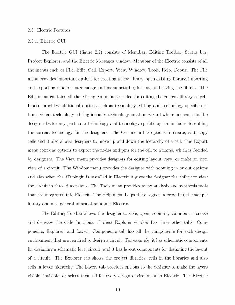
2.3. Electric Features
2.3.1. Electric GUI
The Electric GUI (figure 2.2) consists of Menubar, Editing Toolbar, Status bar,
Project Explorer, and the Electric Messages window. Menubar of the Electric consists of all
the menus such as File, Edit, Cell, Export, View, Window, Tools, Help, Debug. The File
menu provides important options for creating a new library, open existing library, importing
and exporting modern interchange and manufacturing format, and saving the library. The
Edit menu contains all the editing commands needed for editing the current library or cell.
It also provides additional options such as technology editing and technology specific op-
tions, where technology editing includes technology creation wizard where one can edit the
design rules for any particular technology and technology specific option includes describing
the current technology for the designers. The Cell menu has options to create, edit, copy
cells and it also allows designers to move up and down the hierarchy of a cell. The Export
menu contains options to export the nodes and pins for the cell to a name, which is decided
by designers. The View menu provides designers for editing layout view, or make an icon
view of a circuit. The Window menu provides the designer with zooming in or out options
and also when the 3D plugin is installed in Electric it gives the designer the ability to view
the circuit in three dimensions. The Tools menu provides many analysis and synthesis tools
that are integrated into Electric. The Help menu helps the designer in providing the sample
library and also general information about Electric.
The Editing Toolbar allows the designer to save, open, zoom-in, zoom-out, increase
and decrease the scale functions. Project Explorer window has three other tabs: Com-
ponents, Explorer, and Layer. Components tab has all the components for each design
environment that are required to design a circuit. For example, it has schematic components
for designing a schematic level circuit, and it has layout components for designing the layout
of a circuit. The Explorer tab shows the project libraries, cells in the libraries and also
cells in lower hierarchy. The Layers tab provides options to the designer to make the layers
visible, invisible, or select them all for every design environment in Electric. The Electric
10

message window shows the result of current and previous actions. For example, if a DRC
check has been done on a circuit, the result whether it passed or failed is shown in this
window. The Status bar has three parts: the first part displays the name of the component
selected, the second part displays the size of the design, the third part shows the current
design environment of the cell and also shows the scale.
2.3.2. Representation
Any graphical CAD system can offer two basic user-interface styles, connectivity,
and geometry. The connectivity approach is used by all schematic capture based systems:
components are placed, and wires are used to connect them. As the system already knows
that the wires connect to the components, the circuit is properly connected, even when they
are moved. Integrated circuit layout systems use the geometry approach. Masks for chip
fabrication are formed by different layers, which are laid in areas of “paint”. The connectivity
is absolutely not present, and any of the pieces of paint can vary the circuit’s topology [28].
For any connectivity information, one has to go through the error-prone “node-extraction”
phase. Electric is different because it uses the connectivity approach for even integrated
circuit layout. For example, for a PMOS transistor, a designer can place PMOS transistors,
contacts, etc. and draw wires such as metal-1, polysilicon-1, etc. to connect them. This
connectivity-based approach shows the geometry and also the connectivity between them.
Electric uses the terms nodes and arcs for the components and wires respectively. For a
detailed explanation, a node is a component in the design environment of Electric and an
arc is a connecting wire and it’s more than that in Electric. They can be made into many
forms with respect to the design environment. Even when the circuit is changed, the arc
remains connected. It is the most important property of arc in Electric. Figure 2.3 shows
the representation of nodes and arcs. A transistor node, poly arc, and a contact node are
shown. Nodes always have ports on them, which are the connection sites for an arc. An arc
always connects to two nodes [2].
Integrated circuit layout tools available in the market are polygon-based or paint-
based tools, whereas Electric is a connectivity based layout tool. Figure 2.4 shows the shows
11

Transistor Node Poly Arc Contact Node
Transistor Node
Contact Node
Poly Arc
Port Port
Actual Layout
Figure 2.3. Representation in the Electric tool.
the nodes and arcs required to build a PMOS transistor in Electric. Figure 2.5 shows the
layers needed to form a PMOS transistor and also the actual layout of a PMOS transistor in
polygon based tools. In polygon–based integrated circuit layout tools, six different layers are
required to form a PMOS transistor. In Electric, a PMOS transistor node itself has N-well,
Active, p-select, and poly layers as per design rules. These layers expand when one changes
the width and length of a node. In a similar way, a P-Active contact has N-well, P-select,
Active, metal-1, and contact layers in it. Even these expand when the designer changes the
length and width. P-active also consists of N-well, P-select, Active layers in it. Whenever
there is a need to alter the size of a transistor, a designer just needs to change the length
and width of these components. Hence, there is no need to redraw the layers, and also, there
will be fewer geometrical errors.
12
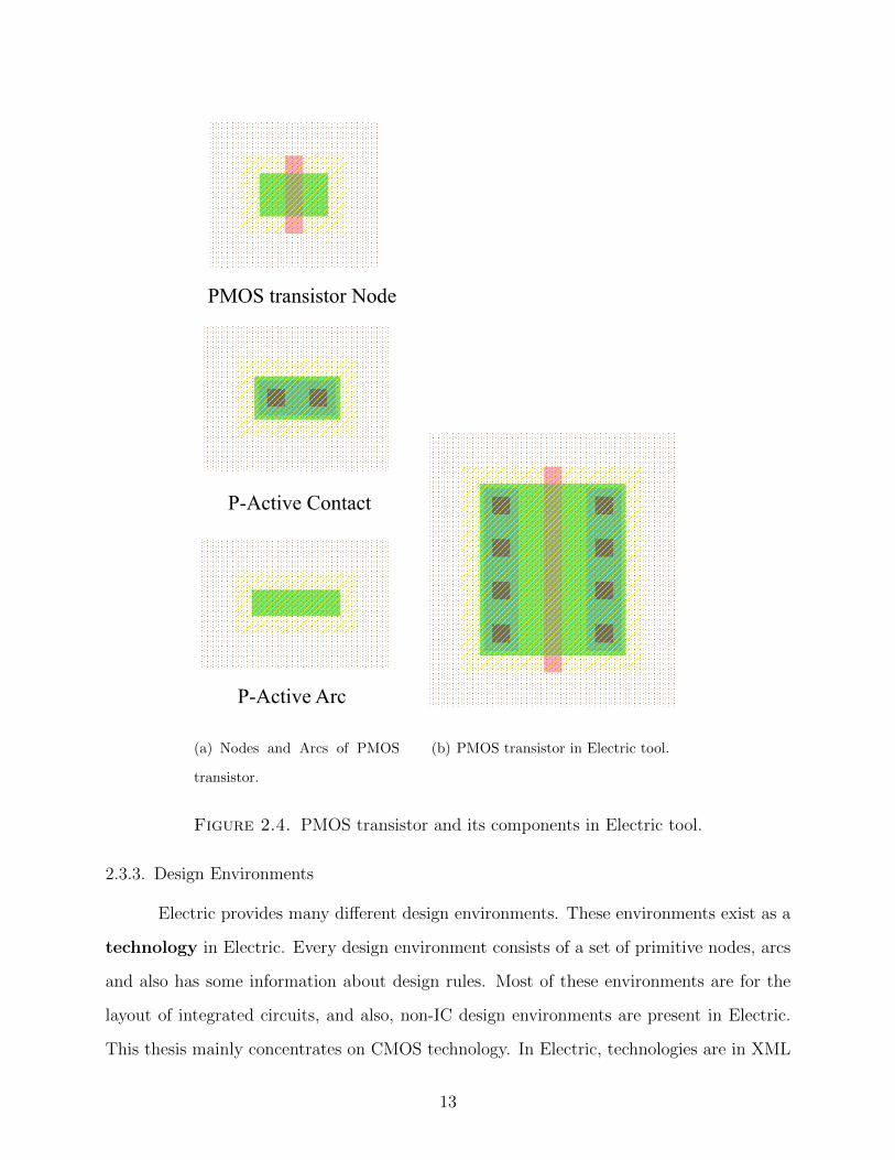
PMOS transistor Node
P-Active Contact
P-Active Arc
(a) Nodes and Arcs of PMOS
transistor.
(b) PMOS transistor in Electric tool.
Figure 2.4. PMOS transistor and its components in Electric tool.
2.3.3. Design Environments
Electric provides many different design environments. These environments exist as a
technology in Electric. Every design environment consists of a set of primitive nodes, arcs
and also has some information about design rules. Most of these environments are for the
layout of integrated circuits, and also, non-IC design environments are present in Electric.
This thesis mainly concentrates on CMOS technology. In Electric, technologies are in XML
13

Contact
Oxide Diffusion
Poly
Metal-1
Pimp (P-plus)
N-well
(a) PMOS transistor layers. (b) PMOS transistor in polygon based tool.
Figure 2.5. PMOS transistor and its layers in polygon-based tool.
format, which contains physical and Electrical details of the foundry process, and they are
attached to the layers which include the design rules, etc. These is Electric-independent in-
formation. It also contains Electric specific information such as primitive nodes and arcs for
designing in Electric. These XML files are automatically generated by Electric by using the
Technology editor and Technology- creation Wizard in Edit menu. Electric allows
the designer to edit the technology by converting the current technology into libraries by
using the command Convert technology to library for editing in Edit/ technology
editing menu. The design environments that are provided by Electric are shown in table
2.2 [28].
2.3.4. Analysis and Synthesis Tools
Since VLSI design has become more complex and very hard to complete the whole
design by hand, there is a need for analysis and synthesis tools. Synthesis tools will cre-
ate or generate circuitry automatically, and analysis tools will verify the circuitry that has
14

Design Envinorment Description
Artwork This design environment provides the components that are used for
drawing graphics and also creating icons for the cell.
BiCMOS It is a semiconductor technology which integrates two separate tech-
nologies such as bipolar junction transistor and the CMOS transis-
tor in an IC.
Bipolar It is a bipolar technology (self-aligned and single poly).
CMOS CMOS is technology, based on an old paper by Griswold Thomas
and it was never got into the actual process which exists as an
illustration.
FPGA FPGA (Field programmable gate array) is an IC technology in Elec-
tric however it is a basic technology which doesn’t have capabilities
of FPGA. It has to be customized by the user with architecture file.
Gem Gem tool is a temporal logic technology in Electric. It is based on
the paper by Lansky A.L and Owicki S.S
MOCMOS It is a CMOS technology that is fabricated by MOSIS project. It
has MOSIS design rules which are similar to lambda rules.
RCMOS RCMOS is the round CMOS technology by Caltech which is an
design environment in Electric.
NMOS It is a technology which uses the only nmos for logic gates and other
digital circuits.
PCB In PCB, Electrical components are connected by conductive tracks,
pads etc which are mechanically supported. Electric’s PCB tech-
nology is very basic and have 8 layers.
Schematic schematic is a design environment where digital and analog
schematic level designs are designed.
Table 2.2. Design Environments in Electric.
15

been designed by hand. Electric comes with many tools which make designing easy for the
user. Analysis tools in Electric are DRC, simulators, and network comparison (LVS) tools.
Synthesis tools in Electric are circuit generators, Routers, etc. To obtain a list of tools in
Electric, the command List Tools in the Tools menu shows all the tools, including which
are active. The list of tools from the menu is shown in figure 2.6.
The JOBS section in cell explorer shows which tools are currently running, and the ER-
RORS section in cell explorer, reports the errors that are generated for the current design.
By using Show Next Error and Show Previous Error commands in menu Edit/ Se-
lection , one can browse the errors that are reported in ERRORS section.
Analysis Tools Synthesis Tools
Design Rule Checker Electric Rule Checker Network Comparison Multiple Simulators
Routers Compactors Circuit Generators Silicon Compilers
Tools
Figure 2.6. List of Analysis and synthesis tools.
16

2.3.4.1. Design Rule Checking
Design rules are necessary for designing any physical level design. These design rules
mainly come from the limitations in manufacturing processes [36, 18]. Attempts to reduce
defects during mask making or constraints in the precision alignment of photolithography
equipment can cause these limitations. The design rule checker ensures that the design is
as per the design rules that are given by the technology manufacturer [32, 19]. In Electric,
there are three types of design rule checkers: Incremental, Hierarchical and Schematic.
• Hierarchical DRC: The Hierarchical design rule checker checks the current cell
design and also the hierarchical design of it. The design rules are already present
in the Electric software for every technology; there is no need to import the Design
rules into Electric. Check Hierarchically command in Tools/DRC menu checks
the hierarchical design of the current cell. Physical level design rules are shown in
figure 2.7.
• Incremental DRC: The Incremental design rule checker runs continuously in the
background as along as the design is being edited. This checker works only on the
physical design level environments such as the mocmos, bicmos, mocmosub, etc., It
examines the layout and issues error messages as it goes. This feature is one of the
best advantages of Electric. The user can make sure the design is as per the design
rules right there, without waiting to finish the design and then run Hierarchical
DRC.
• Schematic DRC: The schematic design rule checker checks the design in the
schematic level. It looks for the nodes whose names are the same as network names
in the cell, arcs that end on another arc without connection between them, etc. The
same Check Hierarchically command in Tools/DRC menu checks the design
when the current cell is in the schematic design environment.
Electric can also read MentorGraphics R© Calibre R© and Cadence R© Assura R© DRC
output files. With the command Import Assura DRC Errors for Current Cell and
Import Calibre DRC Errors for Current Cell from Tools/DRC menu. Figure 2.7
17

shows the fundamental design rules used to design all the physical designs in mocmos tech-
nology
N-Well N-Well N-Well P-Well
A1=12
A2=6 A3=18 A4=0
Poly-1 Poly-1 Active
B1=2
B2=2 B3=1
B4=2
Similar for both transistors
Metal-1Metal-1 Metal-1Metal-1
Metal-1-Polysilicon-1-Con
Metal-1-Metal-2-Con
C1=3
C2=3
D1=3 D2=3
D3=3
Active
Contact
Poly-1
D4=2
Via
D5=2
Metal-6 Metal-6
Via-5
E1=5
E2=5
E3=3
A. N-well Rules
B. Poly Rules
C. Metal-1,2,3,4,5 Rules
D. Contact and Via Rules E. Metal-6 Rules
Figure 2.7. list of fundamental design rules.
18

A N-Well Rules
A1 Minimum N-well width 12λ
A2 Minimum spacing between wells at same potential 6λ
A3 Minimum spacing between wells at different potential 18λ
A4 Minimum spacing between wells of different type 0
B Poly Rules
B1 Polysilicon minimum width 2λ
B2 Minimum spacing over field 3λ
B3 Minimum spacing over active 1λ
B4 Minimum extension over active 2λ
C Metal-1,2,3,4,5 Rules
C1 Minimum width of a Metal 3λ
C2 Minimum spacing between metals 3λ
D Contact and Via-1,2,3,4 Rules
D1 Minimum distance between contact and metal 3λ
D2 Minimum distance between contacts 3λ
D3 Minimum spacing between contact to poly 2λ
D4 Exact size of a Via 2X2
E Metal-6 and Via-6 Rules
E1 Minimum width 5λ
E2 Minimum spacing 5λ
E3 Exact size of a via-6 3X3
Table 2.3. List of fundamental design rules.
19

2.3.4.2. Electrical Rule Checking
Electric comes with two types of Electric rule checker, Well and Substrate checking
and Antenna Rule Checking. The Well Checker checks whether there are well contacts in
every area of the well. It also checks whether the power and ground connections are in the
appropriate places and checks the spacing rules between well areas. Checking spacing rules
can also be done by DRC (Design Rule Checker) after checking the option in the preferences
section. The command Check Wells in Tools/ERC menu will check the wells in the design.
Antenna Rule Checker checks the antenna rules for the design. Antenna rules are necessary
during fabrication of IC’s to make sure that the transistors are not destroyed in that process.
In the fabrication process, to form poly and metal layers the wafer is bombarded with ions.
These ions should travel to the substrate and active layers through the wafer. If the poly or
metal has a large area and if it only connects to gates of the transistor and is not connected
to the source and drain, then ions could travel through the transistors. If the ratio between
area of poly or metal to the area of the transistor is too large, then the transistors will be
destroyed [35]. The command Antenna Check in Tools/ERC will check the antenna rules
for the design [9].
2.3.4.3. Simulation
Electric comes with two built-in simulators, IRSIM and ALS. IRSIM is not available
through the Electric jar file due to license restrictions. It is an open-source gate-level simu-
lator created at Stanford university. The easiest way to get the IRSIM simulator is to build
Electric software from its source code. Electric can create input decks for Verilog simulation
and can also create input decks for spice simulations. The command Write Verilog Deck
in Tools/Simulation (Verilog) menu can produce Verilog decks and the command Write
Spice Deck in Tools/Simulation (Spice) menu can produce spice decks. Electric doesn’t
have Verilog simulator to simulate the input decks and it only has gate level simulator to
simulate the digital designs. One can setup LTspice to simulate the design from Electric.
Ina similar way HSPICE can also be set up. HSPICE is an industry standard SPICE sim-
ulator for over 25 years. It allows accurate circuit simulations which are trusted by many
20

IC design manufacturers. LTSPICE is a free SPICE simulation software, designed by Linear
Technology. It has schematic capture to design the schematic circuits and waveform viewer
to analyze the simulation results.
2.3.4.4. Routing
Routing in EDA tools adds wires to components in the design. In Electric there are
4 different types of routers maze-router, river-router, sea-of-gates router, clock-router and
based on A* and the Lee/Moore algorithms there are 6 experimental routers. From Tool-
s/Routing one can choose different types of routing methods [4].
2.3.4.5. Network Consistency Checking
LVS (Layout vs. Schematic) is the tool which checks the layout design to match with
the schematic design. In Electric, Network consistency checking (NCC) is used to check two
network designs even two layout designs, two schematics designs, layout vs. schematic de-
sign, etc. With the command Schematics and layout views of cell in current window
in the Tools/NCC menu one can check the network of both cells. It is one of the important
features in Electric, the designer can check anytime and for any cell. [38].
2.3.4.6. Placement
Right placement is necessary for the chip to perform efficiently as it will affect the
chip performance and also causes manufacturability problems. In Electric there are differ-
ent types of algorithms and different types of placement. With the command Floorplan
and Place Current Cell in Tools/Placement menu one can place the current cell using
existing algorithms. Force Directed is one of the algorithm that gives good results within
seconds. Genetic algorithm is one of the algorithms in Electric for placing that needs long
runtimes. These are few types of placement algorithms that are present in Electric.
21

2.3.4.7. Compaction
The Compaction tool reduces the space between the components to minimal design
rule spacing in the layout design. This tool helps the user to make room for many other
components in the given area. Electric has not stated the algorithm it uses. It does all
single-axis compaction, horizontal and vertical directions until there is no space left in the
circuit. Do compaction command in Tools/Compaction menu will perform the function.
[9].
2.3.4.8. Silicon Compiler
Silicon Compiler is a tool which can generate a layout from the user’s input VHDL
or Verilog code. It was founded by Johannsen, Mead and Cheng in 1981. Though Electric
has the tool it has not worked well. It converts VHDL code to the netlist for the QUISC
tool. QUISC is a tool that can do place and route of a cell from schematic or structural
VHDL description. The command to use the silicon compiler is Convert Current Cell to
Layout from the Tools/silicon compiler menu.
2.3.5. External Interfaces
For compatibility with other EDA systems, Electric supports many popular inter-
change and manufacturing formats. Importing and exporting the formats can be done using
the commands Import and Export in File menu. Many of these formats don’t come with
circuit connection information. The node extractor in Electric can be used to convert these
pure-layer nodes to Electric components.
• CIF: CIF is abbreviated as Caltech Intermediate Format and was designed by
Caltech. It was originally designed to describe Integrated Circuits. A CIF file
consists of textual commands which set layers and draw on them. CIF is old but
still in use. The last publication on CIF file format was published on Feb 11, 1980,
by the California Institute of Technology.
22

• GDS II: GDS II is an industry standard format for exchange of IC layout artwork.
Previously, it was not an open industry standard. It was designed and owned by
Calma. Later, it was moved to GE [28]. GDS II file format is the final output for
any IC design cycle.
• DXF: AutoCAD DXF is abbreviated as Drawing Interchange Format, which is
controlled and defined by AutoDesk. It is developed to represent the data used in
CAD systems. Almost every type of data can be represented in DXF file format.
• Verilog and VHDL: Verilog and VHDL are hardware description languages. Elec-
tric can import and export to these languages. Electric has two issues with Verilog;
Electric has a weak and old parser which can’t handle standard Verilog code. The
second problem with Electric is that it can’t handle behavioral Verilog. Therefore,
it cannot understand some of the Verilog code.
• Eagle, Pads, ECAD: Eagle is an interface to CadSoft’s EAGLE schematic design
system. Pads is an interface to Mentor’s PADS schematic design system. ECAD is
an interface to ECAD schematic design system.
• Gerber, SVG, Postscript: Gerber is a PCB artwork file format. It contains all
the information related to PCB layers required for fabrication. SVG is abbreviated
as Scalable Vector Graphics; it is based on the XML language. It is used to capture
the current cell window. Postscript is an Adobe printing language which is used to
capture the current cell window.
2.3.6. Parasitic Extraction
Parasitic capacitance and resistance of the interconnect influences and affects the
performance of VLSI circuits. With the decrease in transistor feature size and increase in
circuit performance (higher speeds) interconnect parasitic effects are becoming more impor-
tant. Hence, there is a need to extract the parasitics from the active devices, and the wire
interconnects of an IC for synthesizing the design. Parasitics are extracted from the sim-
ulations of the physical design of an IC using analog/SPICE simulators. Electric provides
the designers to extract the parasitics from the layout, using preferences of Electric, under
23
Tools/parasitic section one has to check the boxes of Extract R and Extract C and
then under Tools/Spice/CDL section one has to choose Conservative RC option for
Parasitics in the same preferences of Electric.
2.4. Design Flow in Electric
Digital and Analog designs in Electric follow the design flow shown in figure 2.8.
2.4.1. Schematic level Design
In Electric, all transistor-level designs are created in the schematics design environ-
ment. It has all the digital, analog and mixed-signal components that are needed to design
the transistor-level designs. Figure 9(b) shows the components required to build the inverter
in transistor-level. It needs a a p-channel transistor, an n-channel transistor, voltage source,
ground, wire, and input and output ports to send input and to get output voltages. The
PMOS is connected to Vdd because it passes strong 1 and NMOS passes strong 0, hence
PMOS is best for pull-up network, and NMOS is best for pull-down network. After de-
signing the transistor level diagram of an inverter the next step is to check for any circuit
connection errors with DRC tool and then simulate the circuit for schematic verification.
LTspice or other SPICE simulators can be used to check the design.
2.4.2. Physical level Design
Once the schematic design is ready, the next step is to translate the schematic design
to device and wire placements on silicon [6]. This level is called physical level. In Electric
the layout of a schematic diagram is drawn in the “mocmos” design environment. There
are many technologies present in Electric as design environments. For a standard CMOS
technology, the user can choose mocmos, mocmossub, etc. depending on the technology
size. For an 180 nm design mocmos is a perfect choice. In Electric for laying out the inverter
at the physical level, we need a P-channel transistor, N-channel transistor, P-well, N-well,
N-active and p-active components. We also need a P-active arc, N-active arc, metal-1 arc
24

Digital Circuit Specifications or Analog Circuit Specifications
Schematic Design Done in Schematic Design Environment Denoted by “Cell_nameSch”
Schematic Verification Run DRC to check schematic Errors
with inbuilt Schematic DRC tool
Schematic Simulation With Write a SPICE deck from Simulation
Tool.
Layout Design Usually for Standard CMOS process it is
done in MOCMOS design environment. Denoted by “Cell_namelay”
Physical Verification Run DRC to check Layout design is as per
rules Run LVS to check Layout vs Schematic. Run ERC to check wells and Antenna rules
Layout Simulation With Write a SPICE deck from Simulation
Tool.
Final Layout
Figure 2.8. Electric Design Flow.
and poly arc. All these arcs are formed when components are connected. Figure 2.10 shows
the components and actual layout design of an inverter using the components. After layout
25
And
Or
Buffer
Flip-Flips
NMOS-Transistor
PMOS-Transistor
Diode
Inductor
Ground
Miscellaneous
Wire Contact
Hierarchical Cells
Bus Pin
Bus Arc
Box
Xor
Mux
Switch
4-Pin NMOS
4-Pin PMOS
Capacitor
Resistor
Vdd
Connection
Port
Spice Components
Pin
Arc
(a) Schematic design components.
PMOS-Transistor
VDD
NMOS-Transistor
Ground
Vout PortVin
Port
(b) Schematic design of an Inverter.
Figure 2.9. Schematic level components and design.
design of an inverter, next step is to check for any layout design errors using DRC. Deign
errors in layout design are harder to rectify than errors in schematic design. LVS ( Layout
vs. Schematic ) is used in this design to check that the layout design is actual representing
the schematic circuit, and then one can check for well and antenna rules if necessary. Layout
simulation can also be done similar to schematic design simulation.
26

Miscellaneous
Hierarchical Cells
Metal-3-Contact
Meta-2-Contact
Polysilicon-2-Contact
Polysilicon-1-Contact
N-Active
P-Active
N-Well
NMOS-Transistor Node
PMOS-Transistor Node
Pure-Layer
Metal-3 Arc, Pin
Metal-2 Arc, Pin
Metal-1 Arc, Pin
Polysilicon2 Arc, Pin
Polysilicon1 Arc, Pin
N-Active Arc, Pin
P-Active Arc, Pin
P-Well
Analog Layers
(a) Physical design layers and components.
N-Well
Polysilicon-1,PMOS-Transistor Node
P-Active
vdd
gnd
Vin Vout
P-Active
PMOS-Transistor
NMOS-Transistor
Metal-1-Pin
Polysilicon-contact
N-Active
Metal-1-Arc
P-Well
(b) Layout design of an inverter.
Figure 2.10. Physical level components and design.
2.5. Scripting in Electric
Electric allows Python and Java programming languages as scripting languages to
run on the software. Scripting helps to automate the design flow. Scripting is used by many
leading EDA companies such as Mentor Graphics, Synopsys, Cadence, etc. to reduce the
time and work needed to establish design flows. It also reduces human errors that may
be caused when designing very large integrated circuits. Python is a widely used high-
level programming language. It supports objects oriented concepts, multiple programming
paradigms, and is also used for scientific computing. Electric uses Jython to run python
scripts and Beam shell plugin to run Java on it. By using scripting languages in Electric,
one can design a circuit in schematics and lay it out in the same technology. Some of the
Python scripts are listed below. The first python script listed creates a layout cell in mocmos
technology and names it as sample1. The classes and methods which are used to create the
27

cell are known from the Javadoc file of Electric. The second python script creates a two
input inverter layout diagram with cell name sample2.
1 from com . sun . e l e c t r i c . database . h i e ra r chy import Ce l l
2 from com . sun . e l e c t r i c . database . h i e ra r chy import Library
3 from com . sun . e l e c t r i c . database . topo logy import NodeInst
4 from com . sun . e l e c t r i c . database . v a r i ab l e import EvalJython
5 from com . sun . e l e c t r i c . techno logy import Technology
6 from java . awt . geom import Point2D
7 newCell = Ce l l . makeInstance ( Library . getCurrent ( ) , ” sample1 l ay ”)
8 tech = Technology . f indTechnology (”mocmos”)
9 trP = tech . f indNodeProto (”P−Trans i s t o r ”)
10 tP = NodeInst . makeInstance ( trP , Point2D . Double (10 , 10) , trP . getDefWidth ( ) , trP
. getDefHeight ( ) , newCell )
11 EvalJython . d i s p l a yCe l l ( newCell )
1 from com . sun . e l e c t r i c . database . h i e ra r chy import Ce l l
2 from com . sun . e l e c t r i c . database . h i e ra r chy import Library
3 from com . sun . e l e c t r i c . database . h i e ra r chy import Export
4 from com . sun . e l e c t r i c . database . prototype import Po r tCha ra c t e r i s t i c
5 from com . sun . e l e c t r i c . database . topo logy import ArcInst
6 from com . sun . e l e c t r i c . database . topo logy import NodeInst
7 from com . sun . e l e c t r i c . database . topo logy import Geometric
8 from com . sun . e l e c t r i c . techno logy import Technology
9 from com . sun . e l e c t r i c . database import Ed i t i ngPre f e r enc e s
10 from java . awt . geom import Point2D
11 from com . sun . e l e c t r i c . t o o l import rout ing
12 from com . sun . e l e c t r i c . u t i l . math import Or i entat i on
13 # crea t e the new c e l l
14 newCell = Ce l l . makeInstance ( Library . getCurrent ( ) , ” sample2 l ay ”)
15 tech = Technology . f indTechnology (”mocmos”)
16 # place a ro ta ted t r a n s i s t o r
28

17 trP = tech . f indNodeProto (”P−Trans i s t o r ”)
18 tP = NodeInst . makeInstance ( trP , Point2D . Double (0 , 20) , 32 , trP . getDefHeight ( ) ,
newCell , Or i enta t i on .R, ”pmos”)
19 # place a metal−Active contact
20 coP = tech . f indNodeProto (”Metal−1−P−Active−Con”)
21 maP = NodeInst . makeInstance ( coP , Point2D . Double (5 , 20) , coP . getDefWidth ( ) , 32 ,
newCell )
22 # place a metal−Active contact
23 coP1 = tech . f indNodeProto (”Metal−1−P−Active−Con”)
24 maP1 = NodeInst . makeInstance ( coP1 , Point2D . Double (−5 , 20) , coP1 . getDefWidth ( ) ,
32 , newCell )
25 # wire the t r a n s i s t o r to the contact
26 aP = tech . f indArcProto (”P−Active ”)
27 ArcInst . makeInstance (aP , tP . f i ndPo r t In s t (” d i f f−bottom”) , maP. f i ndPo r t In s t (”
metal−1−p−act ”) )
28 # wire the t r a n s i s t o r to the contact
29 ArcInst . makeInstance (aP , tP . f i ndPo r t In s t (” d i f f−top ”) , maP1 . f i ndPo r t In s t (”metal
−1−p−act ”) )
30 # place a ro ta ted t r a n s i s t o r
31 trP1 = tech . f indNodeProto (”N−Trans i s t o r ”)
32 tP1 = NodeInst . makeInstance ( trP1 , Point2D . Double (0 , −7) , 22 , trP1 . getDefHeight
( ) , newCell , Or i entat i on .R, ”nmos”)
33 # place a metal−Active contact
34 coN = tech . f indNodeProto (”Metal−1−N−Active−Con”)
35 maN = NodeInst . makeInstance (coN , Point2D . Double (5 , −7) , coN . getDefWidth ( ) , 22 ,
newCell )
36 # place a metal−Active contact
37 coN1 = tech . f indNodeProto (”Metal−1−N−Active−Con”)
38 maN1 = NodeInst . makeInstance ( coN1 , Point2D . Double (−5 , −7) , coN1 . getDefWidth ( ) ,
22 , newCell )
39 # wire the t r a n s i s t o r to the contact
29

40 aP1 = tech . f indArcProto (”N−Active ”)
41 ArcInst . makeInstance (aP1 , tP1 . f i ndPo r t In s t (” d i f f−bottom”) , maN. f i ndPo r t In s t (”
metal−1−n−act ”) )
42 # wire the t r a n s i s t o r to the contact
43 ArcInst . makeInstance (aP1 , tP1 . f i ndPo r t In s t (” d i f f−top ”) , maN1. f i ndPo r t In s t (”
metal−1−n−act ”) )
44 #poly to poly connect
45 poly2=tech . f indArcProto (” Po l y s i l i c on −1”)
46 p2p=ArcInst . makeInstance ( poly2 , tP . f i ndPo r t In s t (” poly− l e f t ”) , tP1 . f i ndPo r t In s t
(” poly−r i g h t ”) )
47 #metal to metal
48 metal1=tech . f indArcProto (”Metal−1”)
49 ArcInst . makeInstance (metal1 , maP. f i ndPo r t In s t (”metal−1−p−act ”) , maN.
f i ndPo r t In s t (”metal−1−n−act ”) )
50 #N−we l l on top
51 nwel l= tech . f indNodeProto (”Metal−1−N−Well−Con”)
52 nwel l1=NodeInst . makeInstance ( nwel l , Point2D . Double (−5 , 38) , 32 , 18 , newCell )
53 cente r=ArcInst . makeInstance (metal1 , nwel l1 . f i ndPo r t In s t (”metal−1−sub s t r a t e ”) ,
maP1 . f i ndPo r t In s t (”metal−1−p−act ”) )
54 ArcInst . g e tTa i lPo r t In s t ( c en t e r )
55 Export . newInstance ( newCell , nwel l1 . f i ndPo r t In s t (”metal−1−sub s t r a t e ”) , ”vdd” ,
Po r tCha ra c t e r i s t i c . IN)
56 pwel l= tech . f indNodeProto (”Metal−1−P−Well−Con”)
57 pwel l1=NodeInst . makeInstance ( pwel l , Point2D . Double (−5 , −22) , 32 , pwe l l .
getDefHeight ( ) , newCell )
58 cente r1=ArcInst . makeInstance (metal1 , pwel l1 . f i ndPo r t In s t (”metal−1−we l l ”) ,maN1.
f i ndPo r t In s t (”metal−1−n−act ”) )
59 Export . newInstance ( newCell , pwel l1 . f i ndPo r t In s t (”metal−1−we l l ”) , ”gnd” ,
Po r tCha ra c t e r i s t i c . IN)
60 #input contact
61 conpoly = tech . f indNodeProto (”Metal−1−Po l y s i l i c on −1−Con”)
30

62 conpoly1 = NodeInst . makeInstance ( conpoly , Point2D . Double (−8 , 4) , conpoly .
getDefWidth ( ) , conpoly . getDefHeight ( ) , newCell )
63 e r c=ArcInst . makeInstance ( poly2 , tP . f i ndPo r t In s t (” poly− l e f t ”) , conpoly1 .
f i ndPo r t In s t (”metal−1−po l y s i l i c o n −1”) )
64 p=ArcInst . getArcId ( e r c )
65 pr in t p
66 #output contact
67 conmet = tech . f indNodeProto (”Metal−1−Pin ”)
68 conmet1 = NodeInst . makeInstance ( conmet , Point2D . Double (10 , 5) , conmet .
getDefWidth ( ) , conmet . getDefHeight ( ) , newCell )
Cell Name
Transistor Node
(a) Layout design of transistor node using
Python script.
Cell name
Design of an Inverter
(b) Layout design of an Inverter using Python.
Figure 2.11. Outputs for scripts running in Electric
.
31

Package Class Method Description
com.sun.Electric.
database.hierarchy
Cell makeInstance() This method creates a cell
com.sun.Electric.
technology
Technology findTechnology() This method finds the re-
quired technology
com.sun.Electric.
technology
Technology findNodeProto() This method returns the
primitiveNode name in that
technology
com.sun.Electric.
technology
Technology findArcProto() This method returns the
ArcProto name in that tech-
nology
com.sun.Electric.
database.topology
NodeInst makeInstance() Creates a NodeInst and do
extra things necessary for it.
com.sun.Electric.
database.topology
ArcInst makeInstance() Creates ArcInst with appro-
priate defaults, connecting
two PortInsts
Table 2.4. Important Methods for Designing in mocmos technology.
2.6. Electric Advantages
• Integrity: It is very rare for an open source EDA tool where schematics and layout
design with simulation are done in one tool. The Electric VLSI design system is a
single user interface where schematics and IC layout designs are done. It has LVS (
Layout vs. Schematic) check to check and compare both designs.
• No node extraction: Node extraction is one of the steps in the design flow for designs
to see connectivity of layout. In Electric there is no need to separately do this step
as it is instantly available with the connectivity part of it. Connectivity is the crucial
thing in physical design level. It must be verified during or right after the design,
32

but most conventional design systems wait for a finished layout. This causes many
errors in the physical layout. The process of converting the design to connected
circuitry from pure geometry is called node extraction.
• No geometry errors: Layers have different minimum geometry rules. In Electric
components which have complex geometries are set as one single component and
can be edited for change of size. Transistor is one such example.
• Simpler design process: In physical design stage of design, designers usually iterate
between DRC (Design rule checking) and Layout vs Schematic (LVS). The problem
is that LVS needs to know the circuit connectivity, which is obtained by the node
extraction process, which can only run after DRC. Hence the layout must be DRC
clean before running LVS. When LVS has problems, one has to edit the layout and
make it DRC clean again, which takes a lot of time. In Electric, the first step is to
know the layout vs schematic errors and then one can easily edit the layout without
fear of losing the LVS match.
• More powerful editing: Because Electric shows the network information even in
Integrated circuit layout, browsing the circuit has become more powerful and gives
a lot of information about it. Since Electric is connectivity based tool, the tools
in Electric make the circuit always connected, even when the circuit is modified on
different hierarchy levels.
33
CHAPTER 3
DIGITAL INTEGRATED CIRCUIT DESIGN USING ELECTRIC
In this chapter, digital circuits are explored with the help of the Electric EDA tool.
A combinational circuit, a sequential circuit, a memory design and an arithmetic logic unit
circuit are chosen for four digital designs in this chapter. All the standard digital circuits
such as Inverter, AND gate, NAND gate, etc. that a student needs to learn are covered in
this chapter, showing the schematic level design, the physical level design and also simula-
tions for that design. All designs are drawn from standard textbooks and existing research
literature. The physical level designs are all drawn, following MOSIS design rules for TSMC
180nm technology. The model files for transistors are taken from the official MOSIS site.
3.1. ALU
The ALU (Arithmetic and Logic Unit) is a main and crucial part in a CPU (Central
Processing Unit). The ALU is used in almost every computing application for all logical and
mathematical operations. It is a multi-functional circuit which can perform many operations
such as AND, NOR, addition, subtraction, etc. without depending on control units. Figure
3.1 shows an 1-bit ALU, which is formed with AND gate, OR gate, full adder, and three
2to1 multiplexers. It performs AND, OR, addition and subtraction operations. Here the
AND gate and OR gates are used for directly performing AND and OR operations and the
full-adder performs the addition and subtraction operations. A multiplexer is used to control
the operations. The other two multiplexers are used for sending the right operation result
to the output. Hence, the 1-bit ALU is formed with six gate level components[27].
3.1.1. Gate level Components
3.1.1.1. Inverter
The inverter is a most important and central block of all digital designs. The working
principle of the inverter is that when the input is connected to ground, the output is pulled
34

AND
Full Adder
INV
2-to-1Mux
1
0
2-to-1Mux
1
0
2-to-1Mux
1
0
ORA
B
Cout Cin
Z
F[1:0]
F[0]
F[1]
Figure 3.1. 1-bit ALU schematic diagram.
to VDD through the PMOS. When the input is connected to the source, the output is pulled
down to ground through the NMOS. The inverter has one p-channel transistor and one n-
channel transistor which are connected to source and ground, respectively [3]. Figure 3.2
shows the transistor level diagram of an inverter. It has a PMOS and NMOS connected in
series, and also a voltage source VDD and ground are connected to these transistors. Figure
3.3 shows the physical diagram of an inverter, the PMOS and NMOS transistors are drawn
as devices. The input port Vin formed with Polysilicon-1 contact and Metal-1 pin is used
for the Vout port. Only Metal-1 arc and polysilicon arc is used for connecting the devices.
The layout area of the implemented Inverter is 58.3µm×12.2.1µm. Figure 3.4 shows the
simulation result for an inverter. When Vin is HIGH the output at Vout is LOW. Similarly,
when Vin is LOW the output at Vout is HIGH.
35

VoutVin
2
10NMOS
2
20PMOS
Figure 3.2. Inverter schematic diagram.
vdd
gnd
Vin Vout
Figure 3.3. Layout Diagram of an Inverter.
36

0 0.5 1 1.5 2 2.5 3 3.5 4x 10
−6
0
1
2
Vin
(V)
0 0.5 1 1.5 2 2.5 3 3.5 4x 10
−6
0
1
2
Simulation Time(us)
Vou
t(V)
Figure 3.4. Simulation results for Inverter.
3.1.1.2. OR gate
The OR gate is one of the basic logic circuits in the combinational logic gates family.
OR gate consists of three series PMOS transistors and three parallel NMOS transistors. It
is formed with NOR gate and an inverter connected to VDD and ground and has two inputs
A and B, and output AORB. When both input signals A and B are lOW, the output AORB
is also LOW. For the other cases the output is always HIGH. Figure 3.5 shows the schematic
diagram of an OR gate. The sizings of the transistors are done as per the technology model
file. The fan-in count of the OR gate is 2, and the fan-out count is 1. Fan-in of a logic
gate is the number of gates present in the input and fan-out is a total number of gates that
are driven by gate output. Figure3.6 shows the layout diagram of an OR gate. The layout
area of the implemented OR gate is 79.32µm×75.1µm. Here for the input signals A and
B polysilicon-1 contact is used and for the output AORB, the metal-1 pin is used. All the
connections are drawn using polysilicon arc and metal-1 arc. Figure 3.7 shows the simulation
results for the OR gate. When VA and VB are LOW the output voltage VAORB is LOW. For
the rest of the cases the output voltage VAORB is always HIGH.
37

B AORB
A
2
10NMOS 2
10NMOS
2
10NMOS
2
20PMOS
2
20PMOS
2
20PMOS
Figure 3.5. Schematic diagram of an OR gate.
vdd
gnd
A
B
AORB
Figure 3.6. Layout diagram of an OR gate.
3.1.1.3. AND Gate
The AND gate is formed with a NAND gate and an inverter. It consists of three
PMOS transistors connected in parallel and three NMOS transistors connected in series.
Figure 3.8 shows the schematic diagram of an AND gate. It has two inputs A and B, and
output ANANDB. When A and B are HIGH, the output AANDB is HIGH. For the rest of the
38

0 0.2 0.4 0.6 0.8 1 1.2 1.4 1.6x 10
−5
0
1
2
VA
(V)
0 0.2 0.4 0.6 0.8 1 1.2 1.4 1.6x 10
−5
0
1
2V
B(V
)
0 0.2 0.4 0.6 0.8 1 1.2 1.4 1.6x 10
−5
0
1
2
Simulation Time(us)
VA
OR
B(V
)
Figure 3.7. Simulation results of an OR gate.
B
AANDBA2
10NMOS
2
10NMOS
210
NMOS
220
PMOS 220
PMOS 2
20PMOS
Figure 3.8. Schematic diagram of an AND gate.
cases the output is LOW. Figure 3.9 shows the layout diagram of an AND gate. Polysilicon-1
contacts are used for the A and B inputs, the metal-1 pin is used for the AANDB output.
Figure 3.10 shows the simulation result of an AND gate. The layout area of the implemented
AND gate is 80.5µm×70.4µm.The result shows the same when A and B input are HIGH,
the output AANDB is HIGH and rest of all cases it is LOW.
3.1.1.4. MUX
The multiplexer is a digital switch that has multiple inputs and a single output. It
chooses one of many inputs and sends a single output through it with the help of control
39

vdd
gnd
A
B
AANDB
Figure 3.9. Layout diagram of an AND gate.
0 0.2 0.4 0.6 0.8 1 1.2 1.4 1.6x 10
−5
0
1
2
VA
(V)
0 0.2 0.4 0.6 0.8 1 1.2 1.4 1.6x 10
−5
0
1
2
VB
(V)
0 0.2 0.4 0.6 0.8 1 1.2 1.4 1.6x 10
−5
0
1
2
Simulation Time(us)VA
AN
DB
(V)
Figure 3.10. Simulation results for AND gate.
inputs. Here a 2 to 1 multiplexer is used to build the 8-bit ALU. Transmission gates are used
to build the multiplexer. A transmission gate is a complementary switch, which is formed
by parallel connection of PMOS and NMOS transistors. Figure 3.11 displays the schematic
diagram of a multiplexer. It is built with two transmission gates and one inverter. A total
of 6 transistors is used to create the multiplexer. Figure 3.12 shows the layout diagram of
the multiplexer. Metal-2 contacts are used for inputs A and B, polysilicon-1 contact and
metal-1 pin are used for the S and Z respectively. The layout area of the implemented MUX
40

is 130.5µm×94.5µm [10].
INV
A
S
B
Z
2 10
NMOS
2 10
NMOS
2 10
PMOS
2 10
PMOS
Figure 3.11. Schematic diagram of a MUX.
3.1.1.5. Full Adder
Adders play a very crucial role in VLSI systems. Microprocessors, digital signal
processing architectures, parity checkers, etc. use adders in their applications. Here a full
28 transistor conventional adder is implemented. In static CMOS, the NMOS passes 0’s,
and PMOS passes 1’s hence the levels will never be degraded. The advantages of CMOS
full adders is that the layout is straight forward since the transistors are complementary,
and it has high noise margins and stability at low voltages due to a complementary pair of
transistors [1]. Other than the A and B inputs it also has a Cin input which is the carry of
the sum from the previous operation. Cout and sum are the outputs of the full adder. Figure
3.13 shows the schematic diagram of a full adder. Figure 3.14 shows the layout diagram of
a full adder. Here polysilicon-1 is used for A and B inputs, and the metal-2 pin is used for
41

vdd
gnd
A
B
S
Z
Figure 3.12. Layout diagram of a MUX.
Cin input. The outputs are formed with metal-1 pins. For connections, poly arc, metal-1
arc, and metal-2 are used in drawing the full adder layout circuit. The layout area of the
implemented adder is 306.9µm×406.2µm. Figure 3.15 shows the simulation results for a full
adder. When A is 1, B is 0, and Cin is 0 the sum is 1 and Cout is 0. Similarly, when A is 1,
B is 0 and Cin is 1 then the sum is 0 and Cout is 1.
3.1.2. Implementation of AN 8-bit ALU
In electric, there is an arc called bus that can be used to connect components similar
to wire. Its advantage is that instead of creating multiple input wires a single bus is used and
can export to multiple inputs. This benefit of a bus is useful in designing schematic circuits
which have multiple inputs and outputs. The ALU has 8-bits A and B inputs and 8-bits of
output Z, carry in and carry out and it also has two extra input bits to choose which function
that ALU should perform. Table 3.1 shows the functions which are performed by the 8-bit
ALU, which can be selected by two bits of F inputs. Table 3.2 shows the binary output
values for a given set of input values. In the simulation of the 8-bit ALU the input A and B
binary values are fixed and then with changing the function bits of ALU the operations AND,
42

Cin
A
B
S
Cout
210
NMOS
210
NMOS
210
NMOS
210
NMOS 210
NMOS
210
NMOS
210
NMOS
210
NMOS 210
NMOS
210
NMOS 210
NMOS
210
NMOS
210
NMOS 210
NMOS
220
PMOS2
20PMOS
220
PMOS
220
PMOS
220
PMOS
220
PMOS 220
PMOS 220
PMOS
2
20PMOS
220
PMOS
220
PMOS
220
PMOS
220
PMOS
220
PMOS
Figure 3.13. Schematic Diagram of a Full Adder.
vdd
gnd
A
B
Cout
Cin
S
Figure 3.14. Layout Diagram of a Full adder.
43

0 0.2 0.4 0.6 0.8 1 1.2 1.4 1.6x 10
−5
012
A(V
)0 0.2 0.4 0.6 0.8 1 1.2 1.4 1.6
x 10−5
012
B(V
)
0 0.2 0.4 0.6 0.8 1 1.2 1.4 1.6x 10
−5
012
Cin
(V)
0 0.2 0.4 0.6 0.8 1 1.2 1.4 1.6x 10
−5
012
Simulation Time(us)
Cou
t(V)
Figure 3.15. Simulation results for a Full adder
addition, subtraction, and OR are performed. Figure 3.16 displays the simulation results
of the 8-bit ALU. The outputs of all Z0 to Z7 are shown in the simulation results. AND
operation is performed by 8-bit ALU till time period 1, addition operation is performed from
time period 1 to 2, OR operation is performed from the time period 2 to 3 and subtraction
operation is performed by 8-bit ALU from time period 3 to 4. Figure 3.17 shows the layout
diagram of an 8-bit ALU. The placement of all the layout blocks of gate level components
results in minimum area. For connections, the metal-1,2,3 arc are used and for inputs and
outputs polysilicon-1, metal-1,2,3 contacts are used. There were no errors in DRC (Design
Rule Checker) check and it also satisfied the LVS (layout vs. schematic) check. The layout
area of the implemented 8-bit ALU is 582.7µm×2357.9µm.
3.2. 2-Bit Multiplier
Multiplication is necessary for the arithmetic operations that are performed by the
processor. In this section, a 2-bit multiplier circuit is used to perform the operation. This
2-bit multiplier circuit consists of two half-adder circuits and 4 AND gate circuits which is
a combinational circuit [16] where the output depends on the inputs and not past output
values. The multiplication is done by the simple sum of the partial products technique and
it is illustrated in figure 3.20. The product of multiplicand and multiplier bits is done using
44

F1 F0 Function
0 0 AND
0 1 ADD
1 0 OR
1 1 SUB
Table 3.1. Func-
tions selected by 2-bit
F inputs
Inputs Value
A 01010001
B 10101100
Outputs Value
AANDB 00000000
AORB 11111101
A+B 11111101
A-B 10100101
Table 3.2. Input
and output values for
8-bit ALU
0 0.5 1 1.5 2 2.5 3 3.5 4
x 10−6
0
1
2
Z0(
V)
0 0.5 1 1.5 2 2.5 3 3.5 4
x 10−6
0
1
2
Z1(
V)
0 0.5 1 1.5 2 2.5 3 3.5 4
x 10−6
0
1
2
Z2(
V)
0 0.5 1 1.5 2 2.5 3 3.5 4
x 10−6
0
1
2
Z3(
V)
0 0.5 1 1.5 2 2.5 3 3.5 4
x 10−6
0
1
2
Z4(
V)
0 0.5 1 1.5 2 2.5 3 3.5 4
x 10−6
0
1
2
Z5(
V)
0 0.5 1 1.5 2 2.5 3 3.5 4
x 10−6
0
1
2
Z6(
V)
0 0.5 1 1.5 2 2.5 3 3.5 4
x 10−6
0
1
2
Simulation Time(us)
Z7(
v)
Figure 3.16. Simulation results for 8-bit ALU.
AND gates to get the partial products then the partial products are added using half-adder
circuits to get 4 bits output that is the final product of 2-bit multiplier. if there is a J bits
multiplier and a K bits multiplicand we need J×K AND gates and (J-1)×K half adders to
get the product for J+K bits.
45

Figure 3.17. Layout Diagram of a Full adder.
3.2.1. Logic Level Components
3.2.1.1. Half-Adder
A typical adder is a digital combinational circuit which is used to add two numbers.
It has two outputs port for sum bit (s) and carry bit (c). Many adders can be realized
for binary numbers, binary coded decimal (BCD), etc. Adder circuits can be used in many
applications in digital electronics. For example, they are used for addressing decoding, table
index calculation, etc. There are two types of adder circuits: Half-adder and Full-adder. In
this section a half-adder circuit is implemented. A half adder circuit adds two numbers and
produces a sum bit(s) and carry bit (c) as outputs. The gate level components of half adder
circuit are XOR and NAND gates. With XOR of A and B, the sum bit is produced and
with A NAND B the carry bit is produced. Half adder circuit adds only two number and
produces sum if there is any carry as input to the half adder, it will be neglected. Hence, it
is called half adder. Figure 3.18 displays the schematic circuit of a half adder. It is formed
with an XOR gate and an AND gate. Figure 3.19 shows the layout diagram of a half adder.
Metal-2 contacts are used for input signal A and B, metal-pin and metal-3 contact is used
for sum bit and carry bit respectively. All the connections are drawn using poly, metal-1,2
arcs. The layout area of the implemented Half-adder is 177.7µm×190.9µm.
46
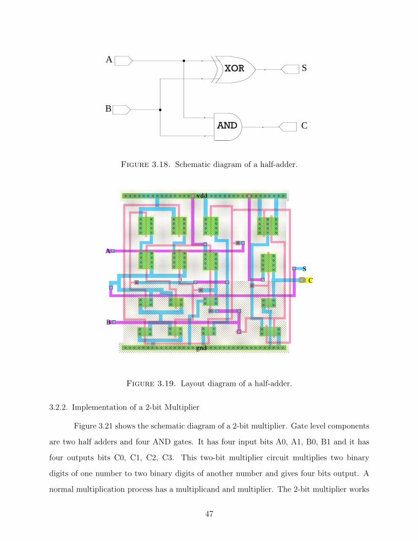
XORA
B
C
S
AND
Figure 3.18. Schematic diagram of a half-adder.
vdd
gnd
A
B
S
C
Figure 3.19. Layout diagram of a half-adder.
3.2.2. Implementation of a 2-bit Multiplier
Figure 3.21 shows the schematic diagram of a 2-bit multiplier. Gate level components
are two half adders and four AND gates. It has four input bits A0, A1, B0, B1 and it has
four outputs bits C0, C1, C2, C3. This two-bit multiplier circuit multiplies two binary
digits of one number to two binary digits of another number and gives four bits output. A
normal multiplication process has a multiplicand and multiplier. The 2-bit multiplier works
47

B1
B0
A1
A0
A0B
0A
0B
1
A1B
0A
1B
1
A0B
0
A0B
1
A1B
0
+
Multiplicand
Multiplier
Partial Product
C0
A1B
1
C1
C2
C3
+PossibleCarry
Final Product
Figure 3.20. 2-bit multiplication process.
on the principle of the sum of partial products: the AND gate in the circuit multiples both
multiplicand bit and multiplier bit to give a partial product. All the partial products from
the AND circuit output are added by the half adder circuit to get the final result. Figure
3.20 shows how the multiplication process is done using the schematic circuit. Here B1 and
B0 are multiplicand bits and A1 and A0 are multiplier bits. A0B1 is a partial product, and
it is added to another partial product A1B0 by a half adder and the result is obtained in
C1. Figures 3.23 and 3.24 show the simulation results for the 2-bit multiplier. When A1
is 0, A0 is 1, B1 is 0 and B0 is 1 then the output C0 is 1 and rest C1, C2, C3 are zero.
Similarly, when When A1 is 1, A0 is 0, B1 is 1 and B0 is 0 then the output C2 is 1 and
rest C1, C0, C3 are zero. Figure 3.22 shows the layout diagram of the 2-bit multiplier. For
inputs and outputs, polysilicon-1, metal-1,metal-2 and also metal-3 contact are used and for
connections poly arc, metal-1,2,3 arc are used. The layout area of the implemented 2-bit
multiplier is 189.9µm×699.0µm.
48
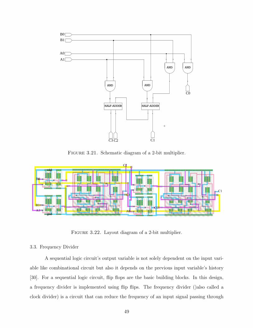
HALF-ADDER HALF-ADDER
B1
A1
A0
B0
C0
C1C2C3
AND AND
AND AND
Figure 3.21. Schematic diagram of a 2-bit multiplier.
C2
C3
C0
C1
B0
B1A1 A0
vdd
gnd
Figure 3.22. Layout diagram of a 2-bit multiplier.
3.3. Frequency Divider
A sequential logic circuit’s output variable is not solely dependent on the input vari-
able like combinational circuit but also it depends on the previous input variable’s history
[30]. For a sequential logic circuit, flip flops are the basic building blocks. In this design,
a frequency divider is implemented using flip flips. The frequency divider ()also called a
clock divider) is a circuit that can reduce the frequency of an input signal passing through
49

0 0.5 1 1.5 2 2.5 3 3.5 4x 10
−6
012
A0(
V)
0 0.5 1 1.5 2 2.5 3 3.5 4x 10
−6
012
A1(
V)
0 0.5 1 1.5 2 2.5 3 3.5 4x 10
−6
012
B0(
V)
0 0.5 1 1.5 2 2.5 3 3.5 4x 10
−6
012
Simulation Time(us)
B1(
V)
Figure 3.23. Input signals for a 2-bit multiplier.
0 0.5 1 1.5 2 2.5 3 3.5 4x 10
−6
012
C0(
V)
0 0.5 1 1.5 2 2.5 3 3.5 4x 10
−6
012
C1(
V)
0 0.5 1 1.5 2 2.5 3 3.5 4x 10
−6
012
C2(
V)
0 0.5 1 1.5 2 2.5 3 3.5 4x 10
−6
012
Simulation Time(us)
C3(
V)
Figure 3.24. Output signals for a 2-bit multiplier.
it. There are various topologies and implementations for frequency dividers. Among all the
divider solutions, the digital frequency divider is preferred because it gives good trade-offs
in the areas of cost, power consumption, and physical dimensions [5]. The typical digital
frequency divider is made with DFF (D flip-flops) or JK flip-flops. Here JK flip-flops are used
to make a digital frequency divider. The JK flip-flops functions as counters which perform
power-of-2 integer divisions [19].
50

3.3.1. Logic level Compoenents
3.3.1.1. JK Flip-Flop
Master Slave JK Flip-flop is used for the frequency divider. At logic level, it consists
of two three-input NAND gates, six two-input NAND gates, and one inverter 3.25. It is
formed by a cascade connection of two S-R Flip-flops with feedback from the output of
second S-R FF to the input of first. The slave will respond to the negative value of the clock
signal since the inverter present is in clock line. Hence, when the clock is HIGH the master
part of JK flip is active, and Slave part is inactive, similarly when the clock is LOW the
master part is inactive, and slave is active. When J=k=0 the output will remain unchanged.
This is because if the Clock is zero the slave will be active and master will be inactive, so
there are no inputs from master to slave hence there is output from the slave. When J=0
and K=1 the output is Q=0 and Q Bar=1, if the clock= one the Master is active, and slave
is inactive. Hence, the outputs of the master are Q1=0 and Q1 Bar=1 so S=0 and R=1. If
the clock is zero the Master is inactive, and slave is active. Therefore, outputs will be Q=0
and Q Bar=1. Again when the clock is one the master is active, and slave is inactive, even
though the output of slave is fed to master the output of master’s remains same, i.e., Q1=0
and Q1 Bar=1. Thus, the outputs are stable from Master and Slave. When J=1 and K=0
the output is Q=1 and Q=0. If the clock is one the Master is active, and slave is inactive.
Therefore, the outputs of the master are Q1=1 and Q1 Bar=0 so S=1 and R=0. If the clock
is zero master is inactive, and slave is active. Therefore, the outputs of the slave will be
Q=1 and Q Bar=0. Hence, the outputs are Q=1 and Q Bar=0. When J=k=1 the output
toggles. If the clock is one Master is active, and slave is inactive, and the output of master
are Q1=1 and Q bar=1 and stays even when the clock is low because when the clock is 0
the master is inactive and the output of slave is not fed to the master. Therefore, the output
toggles and avoid racing effect of the JK flip-flop.
Figure 3.30 shows the digital frequency divider with two JK flip-flops connected in series.
The output of 1st JK flip-flop is given as input to the second flip-flop. The inputs of both
flip-flops J and K are supplied with VDD otherwise J and K are made HIGH. When the clock
51

NAND
NAND
NAND
NAND
NAND
NAND
NAND
NAND
INV
CLK
J
K Q_Bar
Q
S
R
Q1
Q1_Bar
Figure 3.25. Schematic diagram of a JK Flip-Flop.
vdd
gnd
CLK
J
K
Q
QB
Figure 3.26. Layout Diagram of a JK Flip-Flop.
is given the output frequency of the 1st JK flip-flop at QA is a division of input frequency by
2. Similarly, the output frequency of 2nd JK flip-flop at QB is a division of input frequency
by 4 (power-of-2 division). Figure 3.26 shows the layout diagram of a JK flip-flop. The
layout area of the implemented JK flip-flop ALU is 189.9µm×347.0µm.
3.3.1.2. NAND Gate
A NAND gate is formed with two PMOS transistors connected in parallel and two
NMOS transistors connected in series. Figure 3.27 shows the schematic diagram of a NAND
gate. The PMOS transistor’s source is connected to VDD and NMOS transistor’s source is
connected to ground. A and B are the inputs of the NAND gate, and ANANDB is the
52

B
AANDBA2
10NMOS
2
10NMOS
210
NMOS
220
PMOS 220
PMOS 2
20PMOS
Figure 3.27. Schematic Diagram of NAND gate.
0 0.2 0.4 0.6 0.8 1 1.2 1.4 1.6x 10
−5
0
1
2
VA
(V)
0 0.2 0.4 0.6 0.8 1 1.2 1.4 1.6x 10
−5
0
1
2
VB
(V)
0 0.2 0.4 0.6 0.8 1 1.2 1.4 1.6x 10
−5
0
1
2
Simulation Time(us)VA
NA
ND
B(V
)
Figure 3.28. Simulation results for NAND gate.
output. When A and B are HIGH the output ANANDB is LOW, rest of all cases the output
is HIGH. Figure 3.28 shows the simulation results for the NAND gate. Figure 3.29 shows
the layout diagram of a NAND gate. Polysilicon-1 contact is used for input A and B, the
metal-1 pin is used for output ANANDB. The layout area of the implemented NAND gate
is 89.9µm×70.0µm.
3.3.2. Implementation of Frequency divider
Figure 3.30 shows the schematic diagram of a frequency divider. It consists of two
JK flip-flops connected in series. The clock is the input and QA, QB are the outputs of
53

vdd
A
B
ANANDB
gnd
Figure 3.29. Layout Diagram of a NAND gate.
the frequency divider. The primary aim of the frequency divider is to divide the frequency
of the signal which passes through it. The frequency divider implemented here divides the
signal by power of two. The clock signal frequency is divided by 2, and the result is obtained
at QA, and similarly, the input clock signal frequency is divided by four and the result is
obtained at QB. Figure 3.32 shows the simulation results of a frequency divider. From the
figure, the input clock frequency is 250 KHz and the output QA signal frequency is 125
KHz (divided by 2) and the output QB signal frequency is 62.5 KHz (divided by 4). Figure
3.31 shows the layout diagram of frequency divider, the inputs and outputs, polysilicon-1
contact, metal-1,2,3 contacts are used. All the connection are drawn using poly, metal-1,2,3
arcs. The layout area of the implemented frequency divider is 224.4µm×788.8µm.
3.4. 1-Bit SRAM
Memory is an essential component of any computing platform. Its primary functions
are sorting data, Instructions, application software, system software and also it stores the
data and instructions during any application’s or program’s execution [19]. SRAM (static
54

CLK
QA QB
J Q
QB
CLK
K
J Q
QB
CLK
K
Figure 3.30. Schematic diagram of a Frequency divider.
CLK QA QB
vdd
gnd
Figure 3.31. Layout diagram of a Frequency divider.
0 0.5 1 1.5 2 2.5 3 3.5x 10
−5
0
1
2
CL
K(V
)
0 0.5 1 1.5 2 2.5 3 3.5x 10
−5
0
1
2
QA
(V)
0 0.5 1 1.5 2 2.5 3 3.5x 10
−5
0
1
2
QB
(V)
Simulation Time(us)
Figure 3.32. Simulation result for Frequency divider.
random access memory) is volatile memory and performs as a cache for processors. The
word static means that it stores a bit electronically without needing periodic refreshing. It is
a volatile memory, so it doesn’t store data permanently, but it provides high-speed buffering
55

BitlineBitline_Bar
Wordline
2
10
NMOS
2
10
NMOS
25NMOS
25
NMOS
PM1
NM1
PM2
NM2
NM4NM3
25
PMOS25
PMOS
Figure 3.33. Schmetic circuit of an SRAM cell.
for processors. The term random access because any bit of data can be accessed at any
time [2]. In this section, a 1-bit SRAM circuit is explained and designed in schematics and
physical level.
3.4.1. 6T-Cell
The 6T-SRAM cell is the traditional SRAM cell which is widely used to build caches
in computing systems. There are various types of SRAMs depending upon the clocking
mechanism; they can be either asynchronous or synchronous SRAMs. 6T-SRAM is mainly
preferable because it provides excellent results in the areas of stability, area, leakage power,
and speed. Figure 3.33 shows the schematic diagram of 1-bit SRAM cell [31, 22]. The binary
signal is stored in two cross-coupled inverters or a latch which is formed by four transistors.
Two NMOS transistors are connected to the latch for reading and writing operations and are
called access transistors. The six transistors are named drive transistors (NM1, NM2), load
transistors (PM1, PM2) and access transistors (NM3, NM4). NM1, NM2 are sized wider
than NM3, NM4 to achieve read stability. Similarly, NM1, NM2 are sized wider than PM1,
PM2 for write stability. Figure 3.34 shows the layout diagram of a 6T-SRAM cell. The
layout area of the implemented 6T-SRAM cell is 66.4µm×67.1µm.
3.4.2. Implemtation of a 1-bit SRAM
The 1-bit SRAM array consists of a 6T-SRAM cell, a Sense-Amplifier, and a PRE-
charge circuit [24]. The voltage across bit lines determines the bit stored in the SRAM cell.
Whenever there is a large circuit of SRAM, getting proper output is difficult. Hence, the
56

vdd
gnd
Bitline Bitline_Bar
Wordline
Figure 3.34. Layout diagram of an SRAM cell.
sense amplifier is used for reliability and stability to the circuitry. The main function of a
sense amplifier is to sense the voltage across the bit lines and raise or lower the voltage levels.
The pre-charge circuit is used to pre-charge the circuit to a voltage VDD/2. Before every
read and write operation, the pre-charge circuit is turned on to set the voltages of bit lines
to VDD/2, and then it is turned off. The sense amplifier is turned on, it senses the voltage
difference and stores a bit in the SRAM cell. Figure 3.35 shows the schematic diagram of
a 1-bit SRAM circuit. Figure 3.37 shows the waveforms of output. The Pre-charge circuit
is turned on before the write operation. Logic 1 is given through Data In signal. Sense
amplifier and write enable (write) are turned HIGH at the same time, and then the word
line (WL) is activated when all inputs are stable. Now, to read the logic 1 from the circuit,
the Pre-charged circuit is re-activated and also Read enable (Read), sense amplifier and word
line signals are activated again simultaneously. This activation of signals, makes Data Out
signal HIGH.
The operation of writing a zero is also similar to writing logic 1. The pre-charge
circuit is turned on before writing zero. Then Data In is made zero or low, sense amplifier
and word lines are activated to store zero in SRAM cell. In a read operation, the zero
57

6T_Cell
INV
Data_Out Data_In
Read Write
WL
BLBL_bar
Sense
210NMOS
2 10NMOS
2 10NMOS
210
NMOS
210
NMOS
210 NMOS 2
10
NMOS
210NMOS
220
PMOS
220
PMOS
220
PMOS
PRE
VDD/2
Figure 3.35. Schematic diagram of an 1-bit SRAM.
reflected through Data out signal. Figure 3.36 shows the layout diagram of a 1-bit SRAM
circuit. The layout area of the implemented 6T-SRAM cell is 196.3µm×150.7µm..
58

vdd
gnd
SenseData_out
Data_In
WLBL BL_Bar
Read
Write
Figure 3.36. Layout diagram of an 1-bit SRAM.
0 0.2 0.4 0.6 0.8 1 1.2 1.4 1.6 1.8 2
x 10−8
0
0.5
1
Dat
a_In
(V)
0 0.2 0.4 0.6 0.8 1 1.2 1.4 1.6 1.8 2
x 10−8
0
1
2
PRE
(V)
0 0.2 0.4 0.6 0.8 1 1.2 1.4 1.6 1.8 2
x 10−8
0
0.5
1
Rea
d(V
)
0 0.2 0.4 0.6 0.8 1 1.2 1.4 1.6 1.8 2
x 10−8
0
0.5
1
Sens
e(V
)
0 0.2 0.4 0.6 0.8 1 1.2 1.4 1.6 1.8 2
x 10−8
0
0.5
1
WL
(V)
0 0.2 0.4 0.6 0.8 1 1.2 1.4 1.6 1.8 2
x 10−8
0
0.5
1
Wri
te(V
)
0 0.2 0.4 0.6 0.8 1 1.2 1.4 1.6 1.8 2
x 10−8
0
0.5
1
Dat
a_O
ut(V
)
Simulation Time(ns)
Figure 3.37. 1-Bit SRAM Timing Waveform.
59
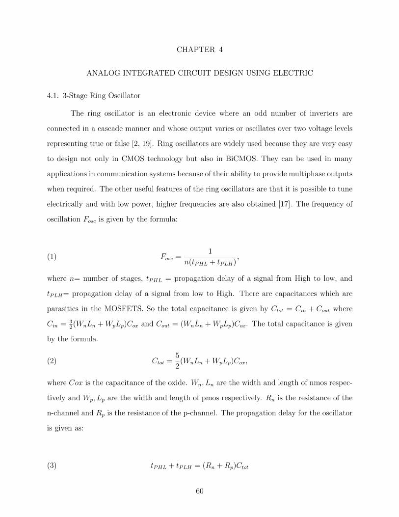
CHAPTER 4
ANALOG INTEGRATED CIRCUIT DESIGN USING ELECTRIC
4.1. 3-Stage Ring Oscillator
The ring oscillator is an electronic device where an odd number of inverters are
connected in a cascade manner and whose output varies or oscillates over two voltage levels
representing true or false [2, 19]. Ring oscillators are widely used because they are very easy
to design not only in CMOS technology but also in BiCMOS. They can be used in many
applications in communication systems because of their ability to provide multiphase outputs
when required. The other useful features of the ring oscillators are that it is possible to tune
electrically and with low power, higher frequencies are also obtained [17]. The frequency of
oscillation Fosc is given by the formula:
(1) Fosc =1
n(tPHL + tPLH),
where n= number of stages, tPHL = propagation delay of a signal from High to low, and
tPLH= propagation delay of a signal from low to High. There are capacitances which are
parasitics in the MOSFETS. So the total capacitance is given by Ctot = Cin + Cout where
Cin = 32(WnLn + WpLp)Cox and Cout = (WnLn + WpLp)Cox. The total capacitance is given
by the formula.
(2) Ctot =5
2(WnLn +WpLp)Cox,
where Cox is the capacitance of the oxide. Wn, Ln are the width and length of nmos respec-
tively and Wp, Lp are the width and length of pmos respectively. Rn is the resistance of the
n-channel and Rp is the resistance of the p-channel. The propagation delay for the oscillator
is given as:
(3) tPHL + tPLH = (Rn +Rp)Ctot
60

4.1.1. Schematic Design
Figure 4.1 shows the schematic diagram of the CMOS inverter based 3-stage ring
oscillator [8]. The factors that change oscillation frequency of the ring oscillator are prop-
agation delay td of a stage and number of stages present in the closed chain loop. The
propagation delay and number of stages are inversely proportional to oscillation frequency.
Hence for higher frequencies the number of stages should be reduced which indirectly reduces
the propagation delay. Reducing number of stages is important because it helps to have more
area in the chips and reduces power consumption too. Here in this section a 3-stage ring
oscillator is designed.
2
10nmos 2
10nmos 2
10nmos
2
20pmos 2
20pmos 2
20pmos
Figure 4.1. Schematic diagram of 3-Stage Ring Oscillator
.
If a square pulse with period T and frequency fclk is given as an input to the inverter,
the current that it must pull from VDD is given as Iavg = VDDCtot
Tand the average power
dissipation of an inverter is given by :
61

(4) Pavg = VDDIavg =V 2DDCtot
T= CtotVDDfclk.
The power delay product (PDP) is often used to compare different technologies or
device sizes; it characterizes the speed of a digital process and it is given by the relation:
(5) PDF = Pavg(tPHL + tPLH).
4.1.2. Physical Design
vdd
gnd
Figure 4.2. Layout Diagram of 3-Stage Ring Oscillator.
The physical design of the 3-stage ring oscillator is shown in figure 4.2. The layout is
drawn as per the design rules of the 180nm TSMC CMOS technology. The Inverter library
is used to design the 3-stage ring oscillator. For connections poly, metal-1 arcs are used and
for contacts polysilicon-1 contact is used.
62
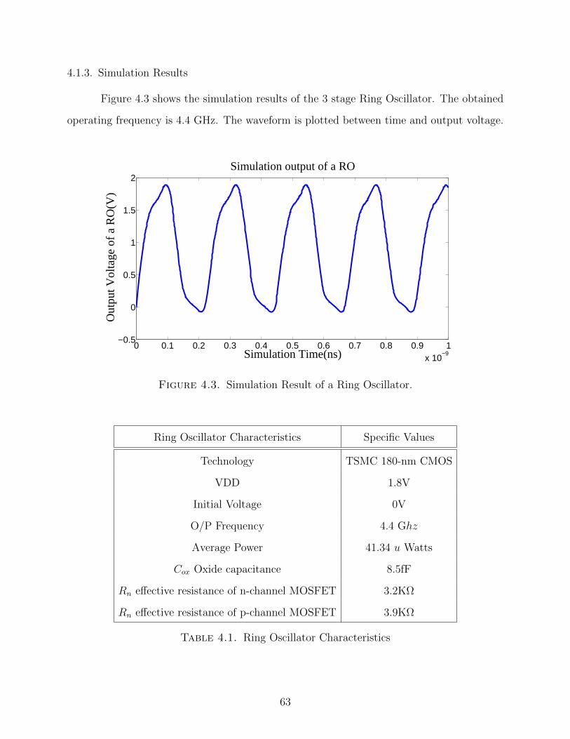
4.1.3. Simulation Results
Figure 4.3 shows the simulation results of the 3 stage Ring Oscillator. The obtained
operating frequency is 4.4 GHz. The waveform is plotted between time and output voltage.
0 0.1 0.2 0.3 0.4 0.5 0.6 0.7 0.8 0.9 1x 10
−9
−0.5
0
0.5
1
1.5
2
Simulation Time(ns)
Out
put V
olta
ge o
f a
RO
(V)
Simulation output of a RO
Figure 4.3. Simulation Result of a Ring Oscillator.
Ring Oscillator Characteristics Specific Values
Technology TSMC 180-nm CMOS
VDD 1.8V
Initial Voltage 0V
O/P Frequency 4.4 Ghz
Average Power 41.34 u Watts
Cox Oxide capacitance 8.5fF
Rn effective resistance of n-channel MOSFET 3.2KΩ
Rn effective resistance of p-channel MOSFET 3.9KΩ
Table 4.1. Ring Oscillator Characteristics
63

4.2. Voltage Controlled Oscillator
The VCO is one of the central components in Pase Locked Loops (PLL), where it is
widely used. A VCO has an odd number of inverters which is similar to Ring oscillator, but
the propagation delays tPHL and tPLH of each inverter are controlled by the current source
and current sink that are present above and below each inverter respectively [9, 19]. Input
voltage controls the output frequency of a VCO.
The schematic diagram of a VCO is shown in figure 4.6. Two high impedance tran-
sistors M1 and M2 are present in the input stage of a VCO. Transistors M4 and M5 operates
as an inverter in the current starved stage. The current source and sink transistor M3 and
M6 limit the current flow to the inverters making them starve for the current [14]. The size
of the transistors and number of inverters factors the oscillation frequency of a VCO.
4.2.1. Schematic Design
For the design equations of a VCO, consider a single inverter with transistors M4 and
M5 shown in the figure 4.4. The capacitance of the inverter is given by Ctot = Cin + Cout
where Cin = 32(WnLn +WpLp)Cox and Cout = (WnLn +WpLp)Cox. The total capacitance of
the inverter is given by:
(6) Ctot =5
2(WnLn +WpLp)Cox,
where Cox is the capacitance of the oxide and Wn, Ln are the width and length of nmos
and Wp, Lp are the width and length of pmos respectively. The total time taken by the
capacitance of an inverter to charge and discharge is given by:
(7) TD,Stage =CtotVDD
ID.
Therefore the oscillation frequency of the VCO is given by:
64

Vin
Vout
2
10nmos
2
10nmos
2
10nmos
2
10nmos
2
10nmos
2
10nmos
2
10nmos
210
nmos
210
nmos
2
10nmos
2
10nmos
M1
M2
M3
M4
M5
M6
text
text
2
20pmos
2
20pmos
2
20pmos
2
20pmos
2
20pmos
2
20pmos
2
20pmos
220
pmos
220
pmos
2
20pmos
2
20pmos
Figure 4.4. Schematic diagram of a 5-stage VCO.
(8) Fosc =1
NTD,Stage
=ID
NCtotV DD
The average current drawn by the VCO is given by Iavg = NVDDCtot
T= N(V DD)CtotFosc.
The average power dissipated by the VCO is :
(9) Pavg = (VDD)Iavg.
4.2.2. Physical Design
Figure 4.5 displays the physical design of the VCO. The Vin input is formed by
using poly arc and Vout is formed with polysilicon-1 contact. The two series PMOS’s are
connected to two series NMOS’s in series. This library is arrayed for four times to form five
stage voltage controlled oscillator and the inverter library is also used here. The layout area
of the implemented VCO is 91.4µm×183.4µm.
65

vdd
gnd
Vin Vout
Figure 4.5. Layout Diagram of the a 5-Stage VCO.
4.2.3. Simulation results
Figure 4.6 shows the simulation results of the 5-stage VCO and table 4.2 shows the
characteristics of the 5-stage VCO. The average power dissipated by is 180 µW. The effective
resistance of n-channel and p-channel MOSFETs are calculated using the TSMC 180 model
file.
0 0.2 0.4 0.6 0.8 1 1.2 1.4 1.6x 10
−8
−0.5
0
0.5
1
1.5
2
Simulation Time(ns)
Out
put V
olta
ge o
f V
CO
(V)
Simulation output of 5−stage VCO
Figure 4.6. Simulation results for 5 stage VCO.
66

Voltage controlled Oscillator Characteristics Specific Values
Technology TSMC 180-nm CMOS
VDD 1.8V
Initial Voltage 0V
Average Power dissipated 180 u Watts
Cox Oxide capacitance 8.5fF
Rn effective resistance of n-channel MOSFET 3.2KΩ
Rn effective resistance of p-channel MOSFET 3.9KΩ
Table 4.2. Characteristics of the 180-nm TSMC CMOS VCO
4.3. Sense Amplifier
4.3.1. Schematic Design
The sense amplifier is one of the main components of memory circuits, and it is used
to sense the bit lines for a 1 or 0 that was written to the cell. Figure 4.7 shows a full-latch
cross-coupled sense amplifier that is fast and reliable [11]. The figure shows the schematic
diagram of sense amplifier. The transistors (M4, M5, M6, M7) form a cross-coupled inverter,
that is a primary component of a sense amplifier. M11, M10, M9 form a Precharge circuit
that precharges the bit lines B0 and B1 to VDD/2 voltage. Transistors M1 and M2 are called
access transistors that are connected to memory cells, and the transistor M3 and M8 are
used as a switch to active and deactivate the sense amplifier [19].
The primary step for reading out a DRAM cell is to precharge the bit lines BL and
BL Bar to VDD
2voltage, which is done by turning on the PRE signal to high with VDD/2
voltage. When the PRE signal is low, the bit line BL and BL Bar have equal VDD/2 volt-
ages, and then a wordline WL is turned ON. That creates the voltage difference between
both bit lines BL Bar and BL where the BL Bar has a higher voltage than that of BL
when a logic 1 is read. The SE signal is raised high which makes the sense amplifier turn
67
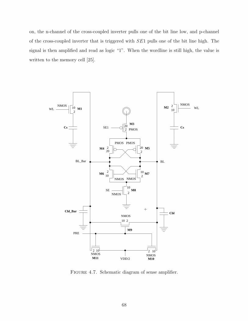
on, the n-channel of the cross-coupled inverter pulls one of the bit line low, and p-channel
of the cross-coupled inverter that is triggered with SE1 pulls one of the bit line high. The
signal is then amplified and read as logic “1”. When the wordline is still high, the value is
written to the memory cell [25].
210
NMOS210
NMOS
210
NMOS
2 10NMOS
2 10NMOS
2
10
NMOS
210
NMOS 210
NMOSM1 M2
M4
M6
M5
M7
Cbl_BarCbl
M3
M8
M11 M10
M9
Cs Cs
220
PMOS
220
PMOS
220
PMOS
BLBL_Bar
PRE
SE
SE1
VDD/2
WL WL
Figure 4.7. Schematic diagram of sense amplifier.
68

4.3.2. Physical Design
Figure 4.8 shows the layout design of a sense amplifier. For the input and outputs
port, metal-1, polysilicon-1, metal-2 contacts are used and for connections polysilicon, metal-
1,2 arcs are used. The layout area of the implemented sense amplifier is 125.3µm×89.1µm.
vdd
gnd
PRE VDD/2
SE1
SE
Figure 4.8. Physical design of sense amplifier.
4.3.3. Simulation Results
Figures 4.10 and 4.9 show the simulation results of the sense amplifier. Figure 4.9 is
the sensing waveform, when the control signals 4.10 are applied to the circuit the Bl, and
BL bar show the results. At first, when the PRE charge signal is applied, both bit lines are
69

0 0.5 1 1.5 2 2.5 3x 10
−8
0
0.2
0.4
0.6
0.8
1
Time(ns)
Vol
tage
(V)
Sensing Waveform
B0B1
Figure 4.9. Sensing Waveform for sense amplifier.
0 0.5 1 1.5 2 2.5 3x 10
−8
0
0.5
1
1.5
2
Time(ns)
Vol
tage
(V)
Control Signals
PREWLSE
Figure 4.10. Control Signals for sense amplifier.
equalized to VDD/2 voltage. Then when wordline is ON, the voltages vary in both bit lines.
This voltage is observed by the sense amplifier when it is turned on. The sense amplifier
amplifies the voltages of both bit lines. Here, in this case, the B0 is logic 0 and B1 is logic
1. Hence, the circuit accurately senses the signals.
70

4.4. Charge Pump
4.4.1. Schematic Design
A charge pump converts the digital signals from PFD to analog signals and supplies
them to the VCO. It consists of two switches, a current source, and a current sink. Charge
pumps are used in PLL’s for a low-cost IC solution. They are also used in LCD drivers,
voltage regulators, piezoelectric actuators, RF antenna switch controllers and many other
electronic systems and their components [19, 15, 7].
A PLL has four important blocks: PFD, Charge pump, Loop Filter and VCO. The
inputs UP and DOWN of the charge pump are the outputs of the PFD. These signals are
regulated by the reference and feedback signals. When the reference signal leads the feedback
signal, the PFD produces UP signal, and when feedback signal leads the reference signal,
it provides DOWN signal [26]. The UP signal that is produced from the PFD will trigger
the Charge pump to inject the charge into the loop filter, increasing the output voltage and
likewise, when the DOWN signal is high, the Charge pump sinks the current out the loop
filter, thus, the output voltage decreases [29]. If ICP is the current of the charge pump the
gain of the charge pump is given by:
(10) KCP =ICP
2π
The current source and sink values should be the same to avoid current mismatching.
Thus, VCO’s control voltage is always the output voltage of charge pump. Figure 4.11 shows
the schematic diagram of a charge pump.
4.4.2. Physical Design
Figure 4.13 shows the layout diagram of the charge pump. Polysilicon-1 contacts
form the up and down input signals, and also the output signal Cpout. The layout area of
the implemented sense amplifier is 121.3µm×144.8µm.
71

Up
DownCPout
210
NMOS
210
NMOS
210
NMOS
210
NMOS210 NMOS
220
PMOS220
PMOS
220
PMOS
220 PMOS
Figure 4.11. Schematic diagram of a Charge Pump.
4.4.3. Simulation Results
Figure 4.12 shows the simulation results of a charge pump circuit. When digital input
voltages are given through Up and Down, the circuit converts them into analog signals and
are given through Cpout.
72
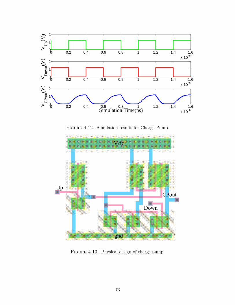
0 0.2 0.4 0.6 0.8 1 1.2 1.4 1.6x 10
−5
0
1
2
VU
p(V)
0 0.2 0.4 0.6 0.8 1 1.2 1.4 1.6x 10
−5
0
1
2
VD
own(V
)
0 0.2 0.4 0.6 0.8 1 1.2 1.4 1.6x 10
−5
0
1
2
Simulation Time(ns)
VC
Pout
(V)
Figure 4.12. Simulation results for Charge Pump.
Vdd
Up
Down
CPout
gnd
Figure 4.13. Physical design of charge pump.
73

CHAPTER 5
CONCLUSION AND FUTURE RESEARCH
5.1. Summary and Conclusions
The VlSI design course has become essential at most Electrical and Computer engi-
neering programs. However, most of the commercial VLSI CAD systems are highly priced
and require high-performance workstations which are not affordable for many academic in-
stitutions. This thesis provides some insight on the open-source EDA tool called Electric
VlSI design system and serves as a user manual for students, teachers and other professionals
who want to develop electric systems in affordable software.
The electric tool shows the best compatibility with all modern operating systems such
as Windows, Macintosh, and UNIX/Linux variants. It also provides important analysis tools
such as DRC (Design Rule Checker), Electric rule checker, Layout vs. Schematic checker
and inbuilt simulators, IRSIM and ASL in a user-friendly interface. Synthesis tools are also
built into electric which include Routers, placement tools, silicon compilers, and generators.
Electric also provides an excellent way of integrating different environments of design. Since
each fabrication process is enclosed in a technology in Electric, there are various technologies
available in electric, but this thesis mainly concentrated on the CMOS technology. It also
extracts the parasitics from the interconnects in the circuit designs. Electric can take python
and java language scripts to design the circuit which automates the design cycle. It exports
and imports many popular interchange and manufacturing formats such as EDIF, GDS-II,
CIF, etc. The design flow for Digital and Analog circuits in electric is similar and very easy
to learn for a student. The digital and analog design circuits are implemented in electric, in
CMOS TSMC 180nm technology in chapter 3 and chapter 4. These simulation results are
accurately correct and also show that electric can easily handle even more complex digital
and analog schematic and layout designs. These designs, which are implemented using
electric, will serve as examples for student projects and also help in further study of electric.
74

However there are some limitations in electric. Firstly it is not capable of designing below
180 nm technology. Secondly, Electric has integrated IRSIM, which only supports digital
simulation, and there is no inbuilt analog simulator. There are solutions for these limitations
in electric itself. One can edit the current technology using the technology creation wizard
in electric. However, it is a daunting and time-consuming process . LTspice, which is a free
circuit simulator, can also be integrated with electric for analog circuit simulations, which
can then overcome this limitation of electric. Because of these reasons, Electric VLSI design
system is expected to be useful the students, teachers and professionals.
5.2. Future Research
As a next step of this research, the digital and analog designs will be implemented
for GNR-FET. Recently a CAD environment for the design, analysis, and layout of CNFET
(Carbon Nanotube Filed-Effect Transistor Circuits) [12] has been created by Steven Rubin,
within electric. This is the first physical design tool for analysis and layout of CNFET
circuits which has been integrated into electric. Electric is a very promising tool for physical
designing and simulation. To further explore the capabilities of the layout designing provided
by electric, designs will be implemented using GNR-FET.
75

BIBLIOGRAPHY
[1] M. Aguirre-Hernandez and M. Linares-Aranda, CMOS Full-Adders for Energy-Efficient
Arithmetic Applications, Very Large Scale Integration (VLSI) Systems, IEEE Transac-
tions on 19 (2011), no. 4, 718–721.
[2] R Jacob Baker, CMOS: circuit design, layout, and simulation, vol. 18, John Wiley &
Sons, 2011.
[3] R Jacob Baker and CMOS Circuit Design, Layout, and simulation, 2004.
[4] Vaughn Betz and Jonathan Rose, VPR: A new packing, placement and routing tool for
FPGA research, Field-Programmable Logic and Applications, Springer, 1997, pp. 213–
222.
[5] J.D. Crockett and M. Siccardi, Power supply noise conversion to phase noise in cmos
frequency digital divider, Frequency Control Symposium and PDA Exhibition, 2002.
IEEE International, 2002, pp. 699–702.
[6] A.H. Farrahi, D.J. Hathaway, M. Wang, and M. Sarrafzadeh, Quality of eda cad tools:
definitions, metrics and directions, Quality Electronic Design, 2000. ISQED 2000. Pro-
ceedings. IEEE 2000 First International Symposium on, 2000, pp. 395–405.
[7] Oleg Garitselov, Saraju P Mohanty, and Elias Kougianos, Accurate polynomial
metamodeling-based ultra-fast bee colony optimization of a nano-cmos phase-locked loop,
Journal of Low Power Electronics 8 (2012), no. 3, 317–328.
[8] , A comparative study of metamodels for fast and accurate simulation of nano-
cmos circuits, Semiconductor Manufacturing, IEEE Transactions on 25 (2012), no. 1,
26–36.
[9] Dhruva Ghai, Saraju P Mohanty, and Elias Kougianos, Parasitic aware process varia-
tion tolerant voltage controlled oscillator (vco) design, Quality Electronic Design, 2008.
ISQED 2008. 9th International Symposium on, IEEE, 2008, pp. 330–333.
[10] Ghai, Dhruva and Mohanty, Saraju P and Kougianos, Elias, A 45nm flash analog to
76

digital converter for low voltage high speed system on chips, Proceedings of the 13th
NASA Symposium on VLSI Design, vol. 3, 2007.
[11] Ali Hajimiri and Raymond Heald, Design issues in cross-coupled inverter sense ampli-
fier, Circuits and Systems, 1998. ISCAS’98. Proceedings of the 1998 IEEE International
Symposium on, vol. 2, IEEE, 1998, pp. 149–152.
[12] Jiale Huang, Minhao Zhu, Shengqi Yang, Pallav Gupta, Wei Zhang, Steven M. Rubin,
Gilda Garreton, and Jin He, A physical design tool for carbon nanotube field-effect
transistor circuits, J. Emerg. Technol. Comput. Syst. 8 (2012), no. 3, 25:1–25:20.
[13] O. Karnalim and R. Mandala, Java archives search engine using byte code as informa-
tion source, Data and Software Engineering (ICODSE), 2014 International Conference
on, Nov 2014, pp. 1–6.
[14] Elias Kougianos and Saraju P Mohanty, Impact of gate-oxide tunneling on mixed-signal
design and simulation of a nano-cmos vco, Microelectronics Journal 40 (2009), no. 1,
95–103.
[15] Jae-Shin Lee, Min-Sun Keel, Shin-II Lim, and Suki Kim, Charge pump with perfect
current matching characteristics in phase-locked loops, Electronics Letters 36 (2000),
no. 23, 1907–1908.
[16] Sharad Malik, Analysis of cyclic combinational circuits, Computer-Aided Design, 1993.
ICCAD-93. Digest of Technical Papers., 1993 IEEE/ACM International Conference on,
IEEE, 1993, pp. 618–625.
[17] MK Mandal and BC Sarkar, Ring oscillators: Characteristics and applications, Indian
Journal of Pure & Applied Physics 48 (2010), 136–145.
[18] S. P. Mohanty, DfX for Nanoelectronic Embedded Systems, 18th December 2013,
Keynote Address, International Conference on Control, Automation, Robotics and Em-
bedded System, Indian Institute of Information Technology, Design and Manufacturing
Jabalpur, India.
[19] , Nanoelectronic Mixed-Signal System Design, no. 9780071825719 and
0071825711, McGraw-Hill Education, 2015.
77

[20] , Energy and Transient Power Minimization during Behavioral Synthesis, Ph.D.
thesis, Department of Computer Science and Engineering, University of South Florida,
Fall, 2003.
[21] Saraju P Mohanty, N Ranganathan, and Vamsi Krishna, Datapath scheduling using
dynamic frequency clocking, VLSI, 2002. Proceedings. IEEE Computer Society Annual
Symposium on, IEEE, 2002, pp. 58–63.
[22] Saraju P Mohanty, Jawar Singh, Elias Kougianos, and Dhiraj K Pradhan, Statistical
doe–ilp based power–performance–process (p3) optimization of nano-cmos sram, INTE-
GRATION, the VLSI journal 45 (2012), no. 1, 33–45.
[23] Saraju P Mohanty, Ramakrishna Velagapudi, and Elias Kougianos, Physical-aware sim-
ulated annealing optimization of gate leakage in nanoscale datapath circuits, Design,
Automation and Test in Europe, 2006. DATE’06. Proceedings, vol. 1, IEEE, 2006,
pp. 6–pp.
[24] Oghenekarho Okobiah, Saraju Mohanty, and Elias Kougianos, Fast design optimization
through simple kriging metamodeling: A sense amplifier case study, Very Large Scale
Integration (VLSI) Systems, IEEE Transactions on 22 (2014), no. 4, 932–937.
[25] Oghenekarho Okobiah, Saraju P Mohanty, Elias Kougianos, and Mahesh Poolakka-
parambil, Towards robust nano-cmos sense amplifier design: a dual-threshold versus
dual-oxide perspective, Proceedings of the 21st edition of the great lakes symposium on
Great lakes symposium on VLSI, ACM, 2011, pp. 145–150.
[26] Jyoti P Patra and Umesh C Pati, Behavioral modeling and simulation of pll based
integer n frequency synthesizer using simulink, International Journal of Electronics and
Communication Engineering 5 (2012), 20.
[27] Medina Ruben, Design, layout, and simulation of an 8-bit alu, http://www.cmosedu.
com/.
[28] Steven M. Rubin, Computer aids for vlsi design, R.L. Ranch Press, 2015, Oracle and
Static Free Software.
78

[29] sarivisetti, Design and optimization of components in a 45nm cmos phase locked loop,
Master’s thesis, Computer Science and Engineering, University of North Texas, 2006.
[30] Hiroshi Shimizu and Masao Kaizuka, Sequential logic circuit, November 10 1987, US
Patent 4,706,217.
[31] Jawar Singh, Jimson Mathew, Saraju P Mohanty, and Dhiraj K Pradhan, A nano-cmos
process variation induced read failure tolerant sram cell, Circuits and Systems, 2008.
ISCAS 2008. IEEE International Symposium on, IEEE, 2008, pp. 3334–3337.
[32] T. Smedes, N. Trivedi, J. Fleurimont, A.J. Huitsing, P.C. de Jong, W. Scheucher, and
J. van Zwol, A drc-based check tool for esd layout verification, EOS/ESD Symposium,
2009 31st, Aug 2009, pp. 1–9.
[33] Rubin Steven, Running electric software from the web, http://java.net/projects/
electric/downloads/download/electric.jnp.
[34] , Website of electric vlsi design system, http://www.staticfreesoft.com/.
[35] Steven M. Rubin, Using the electric vlsi design system, R.L. Ranch Press, 2015, Oracle
and Static Free Software , ISBN 0972751432.
[36] Stephen M Trimberger, An introduction to cad for vlsi, Springer Science & Business
Media, 2012.
[37] Laung-Terng Wang, Yao-Wen Chang, and Kwang-Ting Tim Cheng, Electronic design
automation: synthesis, verification, and test, Morgan Kaufmann, 2009.
[38] Neil HE Weste and Kamran Eshraghian, Principles of cmos vlsi design: a systems
perspective, NASA STI/Recon Technical Report A 85 (1985), 47028.
79