harmonic correction in power supplies feeding non- linear
TRANSCRIPT

Harmonic Correction in Power Supplies Feeding Non-
Linear Loads
Panagiotis Dimitriadis
Brunel University, London
Mohamed Darwish
Brunel University, London
Abstract – This paper focuses on the design of an electronic
circuit which can be used in conjunction with the power
supplies used at the input of non-linear loads (computers,
TV sets, etc.) in order to filter out the input current
harmonics in such loads. The electronic circuit will fill the
gaps of the distorted current waveform so that it becomes
sinusoidal and also in phase with the mains supply. In this
paper different configurations of the proposed electronic
circuit are covered (depending on the location with respect
to the non-linear load). An optimization algorithm is carried
out in order to find the best location, minimum device rating
for different type of loads. The proposed circuit monitors the
input current, output voltage and power rating of the power
supply. The circuit will then decide whether to filter the
input current harmonics or the output voltage harmonics.
The circuit will also optimize the best switching frequency
for the required load so that the power supply operates at
the maximum possible efficiency.
Index Terms – Power electronics, the event of Current
distortion in AC – CD power supply systems, Harmonic
analysis and Harmonic Distortion, suggested methods for
current correction.
I. INTRODUCTION
In AC/DC power supplies, the use of smoothing capacitor
causes a much distorted input current waveform. This is
mainly due to the fact that the input current at the AC side
is a reflection of the charging and discharging current of
the capacitor at the DC side. A typical Total Harmonic
Distortion (THD) of the input current in such power
supplies is greater than 100%, depending on the value of
the filtering capacitance. Although a single computer
may cause very little distortion, however in a buildings
with more than 500 or 1000 computers, the distortion can
be sever causes voltage distortion at the feeder and this
may cause problems to other loads including linear loads
[1-2]. Some of these problem many include [3, 10]
Heating of induction motors.
Heating of transformers.
Heating of capacitors.
Overloading of neutrals.
Telephone transmission interference.
The harmonic distortion caused by an electronic circuit,
according to IEEE standards, must not exceed a total of
5% [12-13], with a maximum of 4% due to any one even
harmonic (i.e., second, fourth, etc) and 2% to any one odd
harmonic (i.e., third, fifth, etc) [12].
II. CURRENT DISTORTION CAUSED BY THE SINGLE PHASE
TWO–PULSE BRIDGE RECTIFIER
The circuit shown in Fig. 1 is a typical bridge rectifier
circuit which could be used in the power supplies of
several applications (TV’s, computers, printers, UPS
systems, etc.)
A smoothing capacitor is usually used to filter out the
output voltage, however this causes the input current to be
discontinuous and full of odd order harmonics. The input
and output current and voltage waveforms are shown in
Fig. 2.
Figure 1. A single phase full wave diode bridge rectifier.
Figure 2. The mains AC voltage supply (c), the distorted current
source (a), and the output voltage (b) of the circuit shown in Fig. 1
Small distributed loads, such as computer loads and TV
sets with switched-mode power supplies at their inputs,
add up to a large increase in the amount of harmonic
current injected in power distribution systems [14]. Fig. 3
D1
D1N5404
D2
D1N5404
D3D1N5404
D4D1N5404
R150 C1
1000u
V1
FREQ = 50VAMPL = 325VOFF = 0
0
V
IV-
V+c
a
b
b
978-1-4799-6557-1/14/$31.00 ©2014 IEEE

illustrates the input current and voltage waveforms of a
television receiver, with a diode rectifier,
Figure 3. Phase voltage (continuous) (a) and phase current (pulsed) (b) to a television receiver [6].
III. CURRENT CORRECTION
A simulation of the input current waveforms shows that
the Total Harmonic Distortion (THD) could be as high as
200% [6]. The FFT analysis of the simulated current
wave form of Fig. 4-a is shown in Fig. 4-b.
Figure 4-a. Distorted power supply input current
Figure 4-b. The FFT analysis of the current waveform shown in Fig. 4-a. .
The Total Harmonic Distortion of the current, according
to the simulation on the circuit of Fig.1, is:
%4.155
554.1418.8
418.8558.15
(%)
22
)(1
2
)(1
2
)(
THD
I
IITHD
RMS
RMSRMSTOTAL
In order to reduce the upper THD (155.4%) to the limits
of 5%, according to the EEE519 standard, the waveform
of the distorted supply current must be transformed to a
sinusoidal form. This paper covers – investigates
different configurations of the proposed electronic circuit
(depending on the location with respect to the non-linear
load), in order to transform the distorted supply current to
a sinusoidal waveform.
Two possible positions for the compensating circuit are
investigated:
- One is to locate the compensator at the dc side of the
load, as shown in Fig. 5.
Figure 5. Compensating circuit located at the dc side of the load.
- The other option is to locate the compensator at the ac
side of the ac/dc converter like the one shown in Fig 6.
Figure 6. Compensating circuit located at the ac side of the ac/dc
converter.
IV. COMPENSATOR LOCATED AT THE DC SIDE OF THE
LOAD
A. Use of Pulse Width Modulation (PWM) technique
A systematic switching sequence is implemented with the
PWM technique where the distorted supply current
(Fig.7-a) is added with an amount of complementary
supply current (Fig.7-b). The idea is that the compensator
current waveform fills the gap or the difference between
the distorted current and the desired sinusoidal waveforms
as shown in Fig.7.
The procedure is as follow: in order to gain a sinusoidal
shape of the current waveform, a sample of the sinusoidal
input voltage is detected (reference signal) and it is
compared to the current waveform (actual signal). The
amplitude of the reference signal must be estimated
according to the ratings of the shape (in voltage) of the
distorted current, having the same frequency and phase
difference of ΔΦ = 1800. Also, there must be: v =
Vmaxsin(π-ωt), where v is the maximum value of the
Time
20ms 22ms 24ms 26ms 28ms 30ms 32ms 34ms 36ms 38ms 40ms 42ms 44ms 46ms 48ms 50ms
-I(V1)
-60A
-40A
-20A
-0A
20A
40A
60A
Frequency
0Hz 0.2KHz 0.4KHz 0.6KHz 0.8KHz 1.0KHz 1.2KHz 1.4KHz 1.6KHz 1.8KHz 2.0KHz
-I(V5)
0A
2A
4A
6A
8A
10A
12A
Voltage Current
a
b
c
a
b
d
voltage and ωt ≈1/3π ( ≈ 58.50), according to the setup of
Fig. 1.
Figure 7. The distorted supply current (a), the complementary supply
current (b), the product sinusoidal source current (c) of the addition of (a) and (b), and the mains supply voltage (d).
After that, the shape of the curve of the complementary
supply current (in voltage), is modulated (Fig.8-a) in
pulses (Fig.8-b) and their complementary (Fig.8-c). These
pulses control a power switching transistor Z1 (Fig.8.c),
in order to pass the complementary supply current, which
is being added with the distorted one, passing through the
Z2 transistor, which is controlled by the complement
pulses (Fig.8-c and Fig.9-b).
Figure 8. (a) A half period of the mains pulse, where the complementary supply current is being modulated.
(b) Modulated pulses. (c) Complementary pulses.
Figure 9. The PWM compensator located at the dc side of the load and
the switching pulses for Z1 and Z2.
The Figure 9 shows how the complementary supply
current is added with the distorted supply current, through
the PWM and boost (L1) technique, by the activation of
the switching devices Z1 and Z2 respectively. R2 acts as
a current control in order to pass the proper amount of the
complementary current. According to i = Imaxsin(ωt), where the i is the peak value of the distorted current and
Imax is the maximum value of the mains sinusoidal current.
Also remember that ωt ≈1/3π (≈ 58.50).
Fig 10 illustrates the mains voltage and the compensated
input current waveform.
Figure 10. The input voltage and the compensated current waveforms
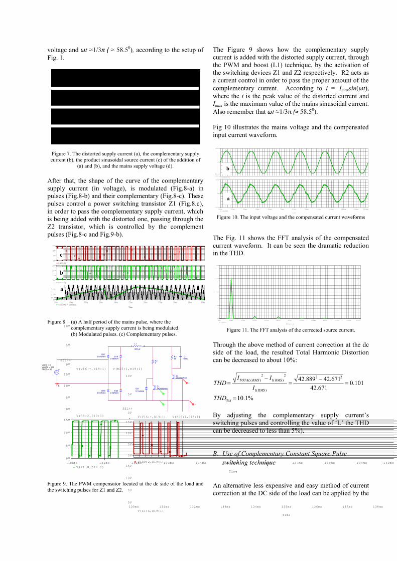
The Fig. 11 shows the FFT analysis of the compensated
current waveform. It can be seen the dramatic reduction
in the THD.
Figure 11. The FFT analysis of the corrected source current.
Through the above method of current correction at the dc
side of the load, the resulted Total Harmonic Distortion
can be decreased to about 10%:
%1.10
101.0671.42
671.42889.42
(%)
22
)(1
2
)(1
2
)(
THD
I
IITHD
RMS
RMSRMSTOTAL
By adjusting the complementary supply current’s
switching pulses and controlling the value of ‘L’ the THD
can be decreased to less than 5%).
B. Use of Complementary Constant Square Pulse
switching technique
An alternative less expensive and easy method of current
correction at the DC side of the load can be applied by the
Time
20ms 21ms 22ms 23ms 24ms 25ms 26ms 27ms 28ms 29ms 30ms
V(V17:+) V(R25:1)
0V
2.5V
5.0V
SEL>>
V(R22:2)
0V
5V
10V
15V
V(R10:2)
0V
5V
10V
15V
Time
20ms 30ms 40ms 50ms 60ms 70ms 80ms 90ms 100ms 110ms 120ms 130ms 140ms
-I(V1)
-100A
0A
100A
V(D17:1)
-400V
0V
400V
SEL>>
Frequency
0Hz 50Hz 100Hz 150Hz 200Hz 250Hz 300Hz 350Hz 400Hz 450Hz 500Hz 550Hz 600Hz
-I(V1)
0A
20A
40A
60A
80A
b
Time
130ms 131ms 132ms 133ms 134ms 135ms 136ms 137ms 138ms 139ms 140ms
V(Z1:G,D19:1)
0V
5V
10V
15V
V(R9:2,D19:1)
0V
5V
10V
15V
V(V16:+,D19:1) V(R25:1,D19:1)
0V
5V
10V
SEL>>
Time
130ms 131ms 132ms 133ms 134ms 135ms 136ms 137ms 138ms 139ms 140ms
V(Z1:G,D19:1)
0V
5V
10V
15V
V(R9:2,D19:1)
0V
5V
10V
15V
V(V16:+,D19:1) V(R25:1,D19:1)
0V
5V
10V
SEL>>
a
c
b
a
Q1
BC547A
Q2
BC547A
Q3
BC557A
R7
10k
R81.5k
R9 7.2
R10
7.2
V+
V-
V+
V-
V+
V-
V+
V-
Q7
BC557A
V16
C:\OrCAD\OrCAD_10.5\PROJECT\ERROR SIGNAL1.txt
Q5
BC547A
Q6
BC557A
R12
10k
R161.5k
R18 7.2
R19
7.2
V8
TD = 0
TF = 50uPW = 0.1u
PER = 300u
V1 = 0
TR = 50u
V2 = 7.5
C5100n
U2
LM7301/NS
+3
-2
V+
7
V-4
OUT6
R25 10k
10k
V12
15VdcR2710k
V1FREQ = 50VAMPL = 325VOFF = 0
Z1IXGH20N60
R150
0
C11000u
Z2IXGH20N60
D17D1N5404 D18
D1N5404
D21
D1N4936D19D1N5404
D20D1N5404
R25
L1
800uH
1 2

use of Complementary Constant Square Pulse Switching
technique. In this technique, the inductor ‘L’ and the
switch Z2 are used to boost the energy in the inductor.
The switching transistor Z2 is operated by square pulses
at 10 kHz and duty cycle 75%. When Z2 is off, switch Z1
is operated ‘complementary’, passing the distorted supply
current of the load as shown in the circuit diagram of Fig.
12.
Fig.12. The Complementary Square Pulse Switching compensator
located at the dc side of the load.
And here also, the control current R2 can be replaced by a
current mirror, which acts as a switched mode (Constant
Square Pulse Switching) current source.
The Fig. 13 show the resulting corrected source current
and the mains voltage.
Figure 13. The resulting corrected source current and supply voltage.
The Fig. 14 shows the FFT analysis of the compensated
source current, where here also, can be seen the high
decrease of the harmonics in order and amplitude.
Figure 14. The FFT analysis of the compensated source current.
Through the above method the resulted Total Harmonic
reaches to:
THD(%) = 4.6%
V. COMPENSATOR LOCATED AT THE OTHER SIDE OF THE
AC/DC CONVERTER
A. Use of Pulse Width Modulation (PWM) technique
The method of the use of PWM technique, which has
been applied at the dc side of the load, is the same being
applied at the other side of the ac/dc converter too.
The Fig. 15 shows a bidirectional switching system,
consisted by a diode bridge rectifier D5, D6, D7, D8 and
transistor Z2, which is being controlled by the
complementary supply current’s switching pulses by the
use of PWM technique; the R17 acts as a current control.
The Fig. 15 also shows the bidirectional switching system
which consists of a diode bridge rectifier D13, D14, D15,
D16 and transistor Z3, which passes the distorted load
current each time just when Z2 is in off position.
The control current R17 can be replaced by a current
mirror, which acts as a switched mode (Constant Square
Pulse Switching) current source.
IV. CONCLUSIONS
The application of the semiconductors in the switching
mode power manipulation, like diode rectifier power
supply with filtering capacitance, results to the distortion
of the supply-source current. The distorted source current
is not sinusoidal any more, with an amount of a Total
Harmonic Distortion (THD) rising up to 150%, as it has
been noticed from the simulation. Considering that the
established value of the THD is 5%, according to IEEE
standards, by switching methods has been achieved firstly
the current correction successfully, where an amount of
source current (complementary to the distorted) is
injected to the dc side of the load, or at the other side of
the ac/dc converter through a compensator circuit. The
current injection either it happens through PWM or
through constant square pulses, by the activation of
transistor switching components (here IGBTs), results to
the correction of the distorted supply current, decreasing
the THD to 10.1% and down to 4.6%. Also the Power
Factor (PF) is not lower than 0.93. In the case where there
is high power distribution systems like buildings with
many non-linear loads, as TV’s, Computers, Printers,
UPS’s etc. one compensator circuit located between
mains supply and input of the ac/dc converter is enough,
after controlling - adjusting the complementary source
current related to the final distorted one. For unique cases,
compensator circuit can be located at the side of the load.
C1
1000u
Z1IXGH10N100A
Z2
IXGH10N100A
L1
10mH
1 2
D5D1N4936
V2
TD = 0us
TF = 1usPW = 75us
PER = 100us
V1 = 0
TR = 1us
V2 = 15
V1
FREQ = 50VAMPL = 325
VOFF = 0
D1
D1N5404
D2
D1N5404
D3
D1N5404
D4
D1N5404
R1
50
0
R2
50
V
I
Frequency
0Hz 0.2KHz 0.4KHz 0.6KHz 0.8KHz 1.0KHz
-I(V1)
0A
5A
10A
Time
40ms 50ms 60ms 70ms 80ms 90ms 100ms
-I(V1)*20 V(D1:1)
-400
0
400

(c)
Figure 15. The PWM compensator (D5, D6, D7, D8, Z2, D13, D14, D15, D16, Z3, L1, and R17) located at the other side of the ac/dc converter (c) and the switching pulses: the PWM modulation of the shape (in volts) of the complementary supply current (a) and the complement of them
(b).
V10
FREQ = 50VAMPL = 325VOFF = 0
0
R175
D21D1N4936
R1610k
Z2IXGH20N60
V+
I
I
I
II
V-
V+
I
V-
R2010k
Q5
BC547A
Q6
BC557A
R12 10k
R211.5k
R22 7.2
Q2
BC547A
R24
7.2
V11
TD = 0
TF = 150uPW = 0.1u
PER = 300u
V1 = 0
TR = 150u
V2 = 6
Q3
BC557A
R7 10k
R81.5k
C5 100n
R9 7.2
VA1
R10
7.2
R25 10k
V7
TD = 0
TF = 150uPW = 0.1u
PER = 300u
V1 = 0
TR = 150u
V2 = 6
10k
V1215Vdc
C4 100n
U8
LM7301/NS
+3
-2
V+
7V
-4
OUT6
VA
R4 10k
10k
V915Vdc
Q4
BC557A
Q7
BC547A
D22D1N4936
Z3IXGH20N60
D13
D1N5404
D14
D1N5404
D15
D1N5404
D16
D1N5404
U7
LM7301/NS
+3
-2
V+
7V
-4
OUT6
D9
D1N5404
D10D1N5404
D11
D1N5404
D12D1N5404
C3
1000u R6
50
D5
D1N5404
D6
D1N5404
L1
100uH
1 2
D7
D1N5404
D8
D1N5404
Time
20ms 21ms 22ms 23ms 24ms 25ms 26ms 27ms 28ms 29ms 30ms
V(R22:2)
0V
5V
10V
15V
SEL>>
V(R10:2)
0V
5V
10V
15V
a
b

REFERENCES
[1] Lin, Weiming ; Cui, Hong ; Zhang, Qiang, “A High Efficiency
Single-stage PFC by Integrating Boost and Buck with Two
Switches”, 35th International Telecommunications Energy
Conference in Smart Power and Efficiency (INTELEC), 2013, pp. 1
– 4.
[2] Da Silva, S.A.O. ; Barriviera, R. ; Modesto, R.A. ; Kaster, M. ;
Goedtel, A., “Single-phase Power Quality Conditioners with series-
parallel filtering capabilities”, IEEE International Symposium on
Industrial Electronics (ISIE), 2011, pp. 1124 – 1130.
[3] Country Voltages
http://www.powerstream.com/cv.htm
[4] V. J. Gosbell, “HARMONIC DISTORTION IN THE ELECTRIC
SUPPLY SYSTEM”, School of Electrical, Computer and Telecommunications Engineering, University of Wollongong, NSW
AUSTRALIA, 2522, March 2000.
[5] Ed. Phillip A. Laplante, “Electrical Engineering Dictionary”,
Boca Raton: CRC Press LLC, 2000.
[6] JOHAN LUNDQUIST, “On Harmonic Distortion in Power
Systems”, Thesis for the degree of licentiate of engineering, Department of Electric Power Engineering, CHALMERS
UNIVERSITY OF TECHNOLOGY Göteborg, Sweden 2001.
[7] Stephen Petersen, “DIODE CHARACTERISTICS”, University
of California, Santa Cruz, Electrical Engineering Department,
Analog Electronics Laboratory, 2013.
[8] Willy Sansen, “Distortion in Elementary Transistor Circuits”,
IEEE TRANSACTIONS ON CIRCUITS AND SYSTEMS—II: ANALOG AND DIGITAL SIGNAL PROCESSING, VOL. 46, NO.
3, MARCH 1999.
[9] Yu-Kang Lo and Chern-Lin Chen, “An Improved Cosine-Mode
Controller for SCR Converters”, IEEE TRANSACTIONS ON
INDUSTRIAL ELECTRONICS, VOL. 42, NO. 5, OCTOBER 1995.
[10] Associated Power Technologies, “Total Harmonic Distortion
and Effects in Electrical Power Systems”, http://www.aspowertechnologies.com/resources/pdf/Total%20Harmo
nic%20Distortion.pdf
[11] Vic Gosbell. “Harmonic Distortion in the Electrical Supply
System,” PQC Tech Note No. 3 (Power Quality Centre), Elliot
Sound Products. http://sound.westhost.com/lamps/technote3.pdf
[12] Energy Supply Association of Australia Limited, “Customer
Guide to Electricity Supply”, Level 2, 451 Little Bourke Street Melbourne, reprinted November 2004.
[13] IEEE Std 519-1992, IEEE Recommended Practices and Requirements for Harmonic Control in Electrical,Power Systems,
New York, NY: IEEE.
[14] Mohamed Darwish, “Harmonic Filters - Passive & Active
Filters and Future Developments”, Brunel UNIVERSITY WEST
LONDON, School of Engineering and Design, 2012.