hft cdr - relativistic nuclear collisions programwieman/hft_cdr_v1hw.doc · web viewcam followers...
TRANSCRIPT

A Heavy Flavor Tracker for STAR
1

A few rules:Please try to use the styles defined for this document. Please do not introduce new styles or modify existing styles unless agreed upon with Flemming or Hans Georg
Normal: body style
Heading: obvious
Caption: Figure and table caption
Figure_spacing: to adjust space before and after figure and to keep the caption attached
List Bullet: for bullet lists
A more detailed manual is the write-up by Jim: “WordFormatingNotes”
2

Table of Content
A FEW RULES:.............................................................................................................................................2
1. INTRODUCTION..................................................................................................................................7
2. PHYSICS MOTIVATION.....................................................................................................................8
3. FUNCTIONAL REQUIREMENTS....................................................................................................11
3.1. MATERIAL BUDGET.........................................................................................................................113.2. INTERNAL ALIGNMENT AND STABILITY..........................................................................................133.3. POINTING RESOLUTION...................................................................................................................113.4. PIXEL INTEGRATION TIME...............................................................................................................133.5. READ-OUT SPEED............................................................................................................................133.6. DETECTOR HIT EFFICIENCY............................................................................................................133.7. LIFE CHANNELS...............................................................................................................................13
4. TECHNICAL DESIGN........................................................................................................................14
4.1. OVERVIEW.......................................................................................................................................144.2. PIXEL...............................................................................................................................................14
4.2.1. Introduction.............................................................................................................................144.2.2. Detector Parameters...............................................................................................................144.2.3. Sensors and Readout...............................................................................................................154.2.4. Sensors and Readout Simulation and Prototyping.................................................................284.2.5. Mechanical Design.................................................................................................................304.2.6. Mechanical Design Simulation and Prototyping................................................................3531
4.3. IST...............................................................................................................................................36 32 4.4. SSD.............................................................................................................................................37 33
4.4.1. SSD Upgrade Design..........................................................................................................37334.4.2. SSD Upgrade.......................................................................................................................37334.4.3. Integration Issues................................................................................................................37334.4.4. Staging Plan........................................................................................................................39354.4.5. Institutional Responsibilities...............................................................................................3935
4.5. INTEGRATION...............................................................................................................................40 36 4.6. SOFTWARE...................................................................................................................................42 37 4.7. COST AND SCHEDULE..................................................................................................................43 38
5. RESOURCES....................................................................................................................................4439
1. APPENDIX 1.....................................................................................................................................4540
5.1. DESCRIPTION OF THE PIXEL RDO SYSTEM.................................................................................45 40 5.1.1. Phase-1 Readout Chain......................................................................................................4540
References..................................................................................................................................................5449
3

List of Figures
FIGURE 1: DIAGRAM SHOWING THE SENSOR DEVELOPMENT PATH OF SENSORS FOR THE STAR PIXEL DETECTOR AT IPHC IN STRASBOURG, FRANCE. THE READOUT DATA PROCESSING REQUIRED IS SHOWN AS A FUNCTION OF SENSOR GENERATION. THE FIRST GENERATION MIMOSTAR SENSORS ARE READ OUT VIA A ROLLING SHUTTER TYPE ANALOG OUTPUT. THE NEXT GENERATION PHASE-1 SENSOR INTEGRATES CDS AND A COLUMN LEVEL DISCRIMINATOR TO.............................................................16
FIGURE 3: FUNCTIONAL BLOCK SCHEMATIC FOR THE READOUT FOR THE PHASE-1 PROTOTYPE SYSTEM. THE DETECTOR LADDERS AND ACCOMPANYING READOUT SYSTEM HAVE A HIGHLY PARALLEL ARCHITECTURE. ONE SYSTEM UNIT OF SENSOR ARRAY / READOUT CHAIN IS SHOWN. THERE ARE TEN PARALLEL SENSOR ARRAY / READOUT CHAIN UNITS IN THE FULL SYSTEM...........................................19
FIGURE 5: PHYSICAL LAYOUT OF THE READOUT SYSTEM BLOCKS. THIS LAYOUT WILL BE THE SAME FOR BOTH THE PHASE-1 BASED PATCH AND THE FINAL PIXEL DETECTOR SYSTEM.....................................19
FIGURE 7: ASSEMBLY OF SENSORS ON A LOW RADIATION LENGTH KAPTON FLEX CABLE WITH ALUMINUM CONDUCTORS. THE SENSORS ARE CONNECTED TO THE CABLE WITH BOND WIRES ALONG ONE EDGE OF THE LADDER..........................................................................................................................................20
FIGURE 9: POWER AND MASS-TERMINATION BOARD BLOCK DIAGRAM. THE DIGITAL SIGNALS TO AND FROM THE SENSORS ARE ROUTED THROUGH THE MAIN BOARD AND CARRIED TO MASS TERMINATION CONNECTORS FOR ROUTING TO THE READOUT BOARDS. LATCH-UP PROTECTED POWER REGULATION IS PROVIDED TO EACH LADDER BY A POWER DAUGHTER CARD MOUNTED TO THE MAIN BOARD. THE MAIN POWER SUPPLIES ARE LOCATED IN THE STAR RACKS.................................................................21
FIGURE 11: READOUT BOARD(S). THE READOUT SYSTEM CONSISTS OF TWO BOARDS PER CARRIER OF 40 SENSORS. A COMMERCIAL XILINX VIRTEX-5 DEVELOPMENT BOARD IS MATED TO A CUSTOM MOTHERBOARD THAT PROVIDES ALL OF THE I/O FUNCTIONS INCLUDING RECEIVING AND BUFFERING THE SENSOR DATA OUTPUTS, RECEIVING THE TRIGGER FROM STAR AND SENDING THE BUILT EVENTS TO A STAR DAQ RECEIVER PC VIA FIBER OPTIC CONNECTION...........................................................22
FIGURE 13: FUNCTIONAL BLOCK DIAGRAM OF THE DATA FLOW ON THE RDO BOARDS..............................22FIGURE 15: EFFICIENCY AND FAKE HIT RATE FOR A SIMPLE THRESHOLD CUT ON PIXEL SIGNAL LEVEL. THIS
FIGURE IS OBTAINED FROM BEAM DATA TAKEN WITH MIMOSTAR-2 SENSORS.....................................23FIGURE 17: SYSTEM LEVEL FUNCTIONALITY DIAGRAM OF THE READOUT OF THE PIXEL SENSORS. ONE OF
THE TEN PARALLEL READOUT CHAINS IS SHOWN..................................................................................24FIGURE 19: DATA RATE REDUCTION IN THE PHASE-1 READOUT SYSTEM.....................................................26FIGURE 21: FUNCTIONAL BLOCK DIAGRAM OF THE RDO BOARDS FOR THE READOUT OF THE ULTIMATE
DETECTOR BASED PIXEL DETECTOR......................................................................................................27FIGURE 23: THREE MIMOSRAT-2 SENSORS IN A TELESCOPE CONFIGURATION USED IN A BEAM, TEST AT
STAR....................................................................................................................................................29FIGURE 25: 200 MHZ DATA EYE PATTERN MEASURED AT THE RDO MOTHERBOARD INPUT TO THE FPGA
(AFTER ALL BUFFERS) AND TRIGGERED ON THE OUTPUT DATA FROM THE FPGA. FULL WIDTH OPENING IN SYSTEM IS ~ 2.3 NS............................................................................................................30
FIGURE 26: FUNCTIONAL SCHEMATIC DIAGRAM FOR ONE PHASE-1 SENSOR BASED RDO BOARD. EACH RDO BOARD SERVICES ONE INNER LADDER AND 3 OUTER LADDERS. EACH LADDER CONTAINS 10 SENSORS............................................................................................................................................46 41
FIGURE 28: BANDWIDTH OF A SINGLE CHANNEL OF THE SIU - RORC FIBER OPTIC LINK AS A FUNCTION OF EVENT FRAGMENT SIZE WITH AN INTERNAL AND EXTERNAL (DDL) DATA SOURCE USING TWO D-RORC CHANNELS. FROM THE LECC 2004 WORKSHOP IN BOSTON...............................................48 43
FIGURE 30: CHRONOGRAM OF THE PHASE-1 BASED READOUT SYSTEM FUNCTIONS FOR A 1 KHZ PERIODIC TRIGGER.............................................................................................................................................49 44
FIGURE 32: CHRONOGRAM OF THE PHASE-1 BASED READOUT SYSTEM FUNCTIONS FOR A 2 KHZ PERIODIC TRIGGER.............................................................................................................................................49 44
FIGURE 34: FUNCTIONAL SCHEMATIC DIAGRAM FOR ONE ULTIMATE SENSOR BASED RDO BOARD. EACH RDO BOARD SERVICES ONE INNER LADDER AND 3 OUTER LADDERS. EACH LADDER CONTAINS 10 SENSORS............................................................................................................................................50 45
4

FIGURE 36: CHRONOGRAM OF THE ULTIMATE SENSOR BASED READOUT SYSTEM FUNCTIONS FOR A 1 KHZ PERIODIC TRIGGER.............................................................................................................................52 47
Figure 38: Chronogram of the Ultimate sensor based readout system functions for a 2 kHz periodic trigger............................................................................................................................................................5348
5

List of Tables
TABLE 1: PERFORMANCE PARAMETERS FOR THE PIXEL DETECTOR...............................................................15TABLE 3: SPECIFICATIONS OF THE PHASE-1 AND ULTIMATE SENSORS.........................................................17TABLE 5: PARAMETERS USED TO CALCULATE DATA RATES FROM A PHASE-1 BASED SYSTEM.....................26TABLE 7: PARAMETERS USED TO CALCULATE DATA RATES FROM A ULTIMATE SENSOR BASED SYSTEM.. . .28TABLE 9: PARAMETERS FOR THE PHASE-1 BASED DETECTOR SYSTEM USED IN THE EXAMPLE
CALCULATIONS SHOWN BELOW.........................................................................................................45 40 Table 11: Parameters for the Ultimate sensor based detector system used in the example calculations
shown below.....................................................................................................................................5146
6

1. IntroductionThe STAR Collaboration proposes to construct a state-of-the-art microvertex detector, the Heavy Flavor Tracker (HFT), utilizing active pixel sensors and silicon strip technology. The HFT will significantly extend the physics reach of the STAR experiment for precision measurement of the yields and spectra of particles containing heavy quarks. This will be accomplished through topological identification of D mesons by reconstruction of their displaced decay vertices with a precision of approximately 50 m in p+p, d+A, and A+A collisions.
The HFT consists of 4 layers of silicon detectors grouped into two sub-systems with different technologies, guaranteeing increasing resolution when tracking from the TPC and the Silicon Strip Detector (SSD) towards the vertex of the collision. The Intermediate Silicon Tracker (IST), consisting of two layers of single-sided strips, is located inside the SSD. Two layers of Silicon Pixel Detector (PIXEL) are inside the IST. The PIXEL detectors have the resolution necessary for a precision measurement of the displaced vertex.
The PIXEL detector will use CMOS Active Pixel Sensors (APS), an innovative technology never used before in a collider experiment. The APS sensors are only 50 m thick and at a distance of only 2.5 cm from the interaction point. This opens up a new realm of possibilities for physics measurements. In particular, a thin detector (0.28% radiation length per layer) in STAR makes it possible to do the direct topological reconstruction of open charm hadrons down to very low pT by the identification of the charged daughters of the hadronic decay.
7

2. Physics MotivationThe primary motivation for the HFT is to extend STAR’s capability to measure heavy flavor production by the measurement of displaced vertices and to do the direct topological identification of open charm hadrons. These are key measurements for the heavy-ion and spin physics programs at RHIC. Heavy quark measurements will facilitate the heavy-ion program as it moves from the discovery phase to the systematic characterization of the dense medium created in heavy-ion collisions as well as obtain a detailed measurement of the nucleon spin structure in polarized p+p collisions. The primary physics topics to be addressed by the HFT include heavy flavor energy loss, flow, and a test of partonic thermalization at RHIC. This program has been identified as key goals for the RHIC program in the Long Range Plan RHIC-II science program and in the RHIC mid-term scientific plan.
From a precise measurement of the spectra and the production ratios of D-meson states, we will be able to extrapolate to the total yield for charm quark production. Furthermore, the open charm production rate is high enough at RHIC that the coalescence process becomes relevant for Charmonium production. Knowledge of the total production cross section for charm quarks is essential as a baseline for J/ measurements. A meaningful answer to the question of whether the J/ mesons are suppressed or enhanced at RHIC requires knowledge of the charm production in heavy-ion reactions.
A heavy quark can be used to probe the properties of the medium created in heavy-ion collisions. The radiation of gluons is kinematically suppressed for heavy flavored quarks passing through the medium: thus they should lose less energy in the dense medium. An important measurement to be made with the HFT is RAA, the ratio of charmed meson production in Au+Au collisions to the binary-scaled production rate in p+p or d+Au collisions. Current measurements using non-photonic electrons as a measure of the abundance of charm and bottom hadrons indicate that the rate of energy loss for heavy quarks is unexpectedly high and inconsistent with our current understanding in pQCD models. Based on the non-photonic electron data the theory of heavy quark energy loss is uncertain and may be completely wrong, especially with regards to bottom.
Another important measurement to be made with the HFT is a measurement of the elliptic flow of D-mesons down to very low pT values. It is generally accepted that elliptic flow is established in the partonic phase. If charm quarks, with a mass much larger than the temperature of the system, undergo elliptic flow then it has to arise from many collisions with the abundant light quarks. Thus, flow of charm quarks can be taken as a probe for frequent re-scatterings of light quarks and is an indication of thermalization that may be reached in the early stages of heavy-ion collisions at RHIC. We believe that proof of thermalization constitutes the last step in the characterization of the strongly interacting matter created at RHIC. These important measurements require a very thin detector to push the measurement down to the lowest momenta where transverse elliptic flow is manifest.
Without the HFT upgrade the STAR experiment will not be able to execute the comprehensive heavy flavor program proposed here. However, STAR has been able to complete some initial charm measurements with the TPC alone, and with the data from
8

the recent Run 7 STAR might be able to make an initial estimate for the B-meson contribution to the spectrum of the non-photonic electrons in Au+Au collisions.
Figure 1: v2 as a function of pT for the case of charm flow the same as light quark flow (red) and for the case where charm does not flow (green).
9
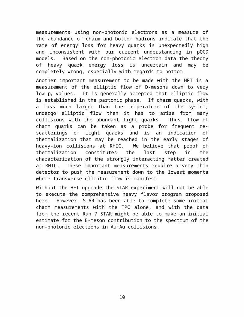
Figure 2: RAA as a function of pT.
We need a plot of C here!!!!!!!
10

3. Functional Requirements
3.1. General Design ConsiderationsSTAR is a large acceptance experiment with full azimuthal coverage at mid-rapidity in the pseudo-rapidity range |n| < 1. With the TPC as a central detector and a current read-out speed of about 100 Hz STAR is considered to be a “slow” detector as far as single particle observables are concerned. Even after the DAQ upgrade to 1000 Hz in 2009 the read-out speed will be limiting the single particle capabilities of STAR. The real strength of STAR, good particle identification and full azimuthal coverage, come into play when correlations or multi-particle final states are studied. Good particle identification and full azimuthal coverage have been the bases for the enormous success of the STAR physics program.
It is obvious that when it comes to identifying rare processes, like heavy flavor production with multi-particle final states, full azimuthal coverage will be of utmost importance. Thus, full azimuthal coverage is a prime design requirement for the HFT.
Another important requirement is to keep a very low overall material budget in order to limit the effects of multiple scattering and of conversions. Our goal is to overall reduce the radiation length of the inner tracking and support system compared to the status when the SVT was the STAR inner tracking detector.
3.2. Pointing ResolutionHeavy flavor hadrons have extremely short life times (c ~ 50 m). Identifying such a short displaced vertex requires extremely good pointing resolution. This is especially important for the identification of low transverse momentum decays where small gains in pointing resolution lead to large gains in detection efficiency. (maybe we can add a graph of efficiency at 1 GeV as fuction of pointing resolution?). The efficiency of D0
detection is given in Figure 3 as a function of pT.
11
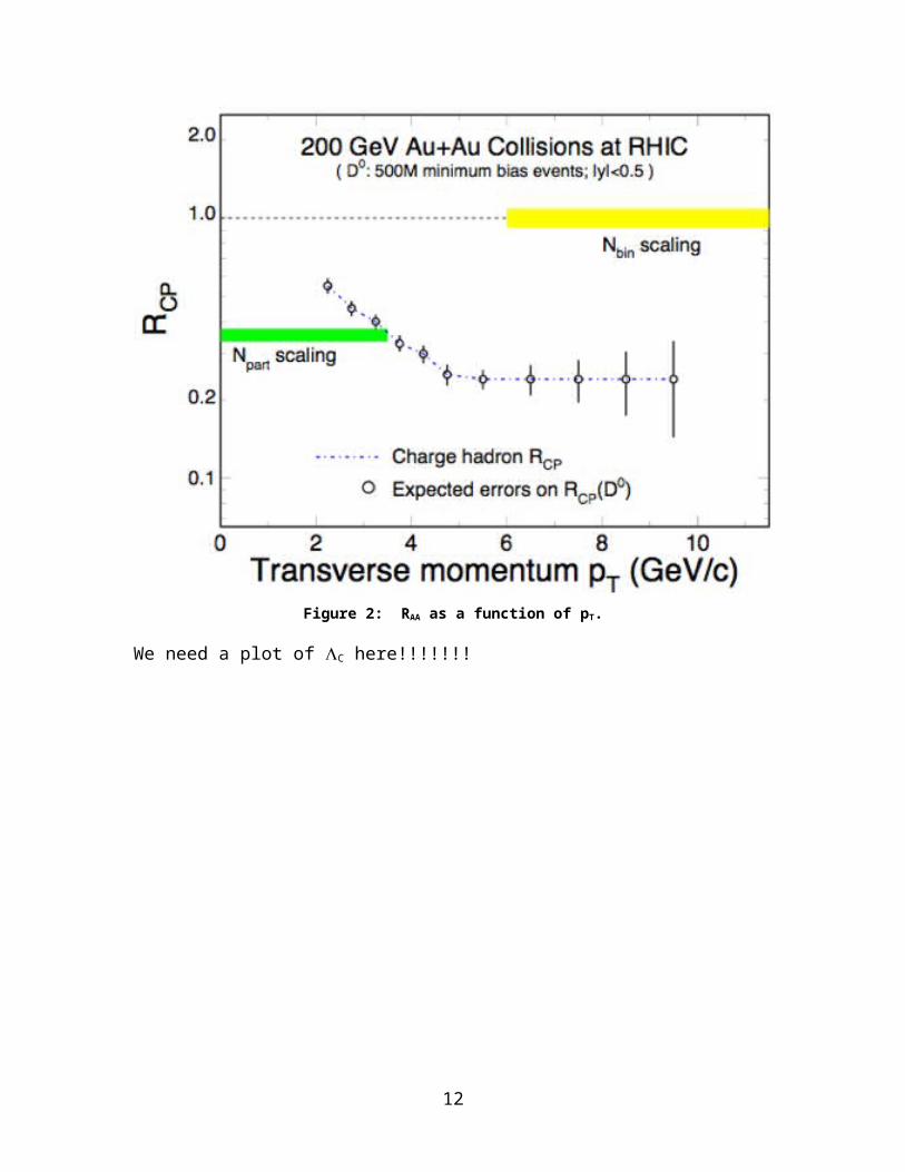
Figure 3: D0 efficiency.
We require a pointing resolution of better than 50 m for kaons of 750 MeV/c. 750 MeV/c is the mean momentum of the decay kanos from D mesons of 1 GeV/c transverse momentum, the peak of the D meson distribution.
The pointing resolution that will be achieved by the HFT can be calculated from the design parameters.
3.3. Multiple Scattering in the inner LayersThe precision with which we can point to the interaction vertex is determined by the position resolution of the pixel detector layers and by the effects of multiple scattering in the material the particles have to traverse. The beam pipe and the first pixel layer are the two elements that have the most adverse effect on pointing resolution. Therefore, it is crucial to make those layers as thin as possible and to build them as close as possible to the interaction point.
We have chosen a radius of 2 cm for a new beam pipe. Making this radius even smaller would make the STAR beam pipe the limiting aperture of the RHIC ring. This is not a desirable situation. The central section of the beam pipe will be fabricated from Beryllium. Such a beam pipe can have a minimal wall thickness of xx m, equivalent to 0.xx % of a radiation length.
The two pixel layers will be at a radius of 2.5 cm and 8 cm, respectively. The sensors will be thinned down to 50 m and the ladders will be fabricated in ultra-light carbon fibre technology. The total thickness of the beam pipe and the fist pixel layer will be the
12

equivalent of 0.xx % of a radiation length. With those parameters, the contributions to the pointing resolution from multiple scattering and from detector resolution will be about equal.
The radiation lengths of the two innermost structures, the beam pipe and the first pixel layer, are design parameters.
3.4. Internal Alignment and StabilityThe Pixel and the IST positions need to be known and need to be stable over a long time period in order not to have an effect on the pointing resolution. The
3.5. Pixel Integration Time
3.6. Read-out Speed
3.7. Detector Hit Efficiency
3.8. Life Channels
13

4. Technical Design
4.1. Overview
4.2. Pixel
4.2.1. Introduction
4.2.2. Detector ParametersThe relevant performance parameters for the Pixel detector are shown in Table 1.
Pointing resolution (13 Å 19GeV/p×c) m
Layers Layer 1 at 2.5 cm radius
Layer 2 at 8 cm radius
Pixel size 18.4 m × 18.4 m
Hit resolution 10 m rms
Position stability 6 m (20 m envelope)
Radiation thickness per layer
X/X0 = 0.28%
Number of pixels 436 M
Integration time (affects pileup) 0.2 ms
Radiation tolerance 300 kRad
Rapid installation and replacement to cover rad damage and other detector failure
Installation and reproducible positioning in a shift
Table 1: Performance parameters for the pixel detector
14

4.2.3. Sensors and Readout
Development and Deployment PlanWe intend to approach the completion of the Pixel detector for STAR as a two stage development process with the readout system requirements tied to the stages of sensor development effort. The sensor development is taking place at the Institut Pluridisciplinaire Hubert Curien (IPHC) in Strasbourg, France where we are working in collaboration with Marc Winter’s group. In the current development path, the first set of prototype sensors to be used at STAR will have digital outputs and a 640 µs integration time. We will use these sensor prototypes to construct a limited prototype detector system for deployment at the STAR detector during the summer of 2010. This prototype system will employ the mechanical design to be used for the final Pixel detector as well as a readout system that is designed to be a prototype for the expected final readout system to be deployed with the final Pixel sensors in a complete detector in the 2012 time frame.
Monolithic Active Pixel Sensor (MAPS) Development at IPHCThe sensor development path for the Pixel detector sensors is tailored to follow the development path of the technology as it was set by the IPHC group. In this path, MAPS sensors with multiplexed serial analog outputs in a rolling shutter configuration are envisioned as the first generation of sensors followed by a more advanced final or ultimate sensor that had a digital output(s). The analog MAPS have been produced and tested and our sensor development path moves to digital binary readout from MAPS with fine grained threshold discrimination, on chip correlated double sampling (CDS) and a fast serial LVDS readout. A diagram showing the current development path and with the attendant evolution of the processing and readout requirements is shown in Figure 4.
15

Figure 4: Diagram showing the sensor development path of sensors for the STAR Pixel detector at IPHC in Strasbourg, France. The readout data processing required is shown as a function of sensor generation. The first generation Mimostar sensors are read out via a rolling shutter type analog output. The next generation Phase-1 sensor integrates CDS and a column level discriminator to give a rolling shutter binary readout with a 640 µs integration time. The final generation Ultimate sensor integrates data sparsification and lowers the readout time to < 200 µs.
The Mimostar series sensors are the generation of sensors that have been fabricated and tested. These are 50 MHz multiplexed analog readout sensors with 30µm × 30µm pixels in variously sized arrays depending on generation. This generation has been tested and characterized and, with the exception of some yield issues, appears to be well understood. Testing with these sensors is well described in a NIM paper reference.
The next generation is named “Phase-1”. This sensor will be based on the Mimosa-8 and Mimosa-16 sensors and will contain on-chip correlated double sampling and column level discriminators providing digital outputs in a rolling shutter configuration. The Phase-1 will be a full sized 640 × 640 array resulting in a full 2 cm × 2 cm sensor size. In order to achieve a 640 µs integration time, the Phase-1 sensor will be equipped with four LVDS outputs running at 160 MHz. The first delivery of wafers of this sensor design is expected in late 2008.
The final sensor is named “Ultimate”. The Ultimate sensor includes all of the attributes of the Phase-1 sensor with the pixel sub-arrays clocked faster to give a <200 µs integration time and the integration of a run length encoding based data sparsification and zero suppression circuit. The pixel size has been reduced to 18.4 µm × 18.4 µm to increase the sensor radiation tolerance in the higher luminosity RHIC II environment. There are two data output lines from the sensor and the data rates are low thanks to the newly included data sparsification circuitry. The first prototypes of this design are expected to be delivered in the 2010 time frame.
Sensor Series SpecificationsThe specifications of the sensors under development are shown in Table 2.
Phase -1 Ultimate
Pixel Size 30 µm × 30 µm 18.4 µm × 18.4 µm
Data Processing in RDO and on chip by generation of sensor.
The RDO system design evolves with the sensor generation.
SensorPixels
AnalogSignals ADC /
Disc. CDS DataSparsification
RDOto
DAQ
Mimostar sensors
Phase-1sensors - 640 us integration time
Ultimate sensors - < 200 us integration time
16

Array size 640 × 640 1024 × 1088
Active area ~ 2 × 2 cm ~ 2 × 2 cm
Frame integration time 640 µs 100 – 200 µs
Noise after CDS 10 e- 10 e-
Readout time / sensor 640 µs 100 – 200 µs
Outputs / sensor 4 2
Operating mode Column parallel readout with all pixels read out serially.
Column parallel readout with integrated serial data sparsification.
Output type Digital binary pixel based on threshold crossing.
Digital addresses of hit pixels with run length encoding and zero suppression. Frame boundary marker is also included.
Table 2: Specifications of the Phase-1 and Ultimate sensors.
The Phase-1 is a fully functional design prototype for the Ultimate sensor which results in the Phase-1 and Ultimate sensors having very similar physical characteristics. After successful development and production of the Phase-1 sensors, a data sparsification system currently under development at IPHC will be integrated with the Phase-1 design. With the additional enhancement of design changes allowing for faster clocking of the sub-arrays, the resulting sensor is expected to be used in the final Pixel detector. In addition to the specifications listed above, both sensors will have the following additional characteristics;
Marker for first pixel Register based test output pattern JTAG selectable for binary readout
troubleshooting. JTAG selectable automated testing mode that provides for testing pixels in
automatically incremented masked window to allow for testing within the overflow limits of the zero suppression system.
Independent JTAG settable thresholds Radiation tolerant pixel design. Minimum of 3 fiducial marks / sensor for optical survey purposes. All bonding pads located along 1 side of sensor Two bonding pads per I/O of the sensor to facilitate probe testing before sensor
mounting.
17

Architecture for the Phase-1 Sensor SystemThe requirements for the Phase-1 prototype and final readout systems are very similar. They include;
Triggered detector system fitting into existing STAR infrastructure and to interface to the existing Trigger and DAQ systems.
Deliver full frame events to STAR DAQ for event building at approximately the same rate as the TPC (~ 1 KHz for the STAR DAQ1K upgrade).
Reduce the total data rate of the detector to a manageable level (< TPC rate)
We have designed the prototype data acquisition system to read out the large body of data from the Phase-1 sensors at high speed, to perform data compression, and to deliver the sparsified data to an event building and storage device.
The proposed architecture for the readout of the Phase-1 prototype system is shown in Figure 5 with the physical location and separation of the system blocks shown in Figure6.
Carrier X10
Ladder X 4
Sensor X 10 LU protectedVoltageRegulators
X 40
LVDS, signal,controlMass TerminationPatch
PowerSupplies
RDO Boards
RDO PCs
Trigger,Control,Monitor
DAQ,Control,Monitor
X 10
X 3
MWC existing
Figure 5: Functional block schematic for the readout for the Phase-1 prototype system. The detector ladders and accompanying readout system have a highly parallel architecture. One system unit of sensor array / readout chain is shown. There are ten parallel sensor array / readout chain units in the full system.
18

1 m –Low mass twisted pair
6 m - twisted pair
Sensors, Ladders, Carriers(interaction point)
LU Protected Regulators,Mass cable termination
RDO BoardsDAQ PCs
Magnet Pole Face(Low Rad Area)
DAQ Room
PowerSupplies
Platform
30 m
100 m - Fiber optic
30 m
ControlPCs
Platform
30 m
1 m –Low mass twisted pair
6 m - twisted pair
Sensors, Ladders, Carriers(interaction point)
Sensors, Ladders, Carriers(interaction point)
LU Protected Regulators,Mass cable termination
RDO BoardsRDO BoardsDAQ PCs
Magnet Pole Face(Low Rad Area)
DAQ Room
PowerSupplies
Platform
30 m
100 m - Fiber optic
30 m
ControlPCs
Platform
30 m
Figure 6: Physical layout of the readout system blocks. This layout will be the same for both the Phase-1 based patch and the final Pixel detector system.
The architecture of the readout system is highly parallel. Each independent readout chain consists of a four ladders mechanical carrier unit with each ladder containing ten Phase-1 sensors. The current plan is to install a patch of Phase-1 sensors consisting of at least two carrier units mounted with the final mechanical positioning structure and positioned with a 120 degree separation. The readout system will be described as if all carriers will be installed since this architecture also extends to the final Pixel system.
The basic flow of a ladder data path starts with the APS sensors. A Pixel ladder contains 10 Phase-1 APS sensors, each with a 640 × 640 pixel array. Each sensor contains four separate digital LVDS outputs. The sensors are clocked continuously at 160 MHz and the digital data containing the pixel threshold crossing information is read out, running serially through all the pixels in the sub-array. This operation is continuous during the operation of the Phase-1 detectors on the Pixel ladder. The LVDS digital data is carried from the four 160 MHz outputs in each sensor in parallel on a low mass flex printed circuit board to discrete LVDS buffers located at the end of the ladder and out of the low mass detector region. This electronics portion of the ladder also contains the buffers and drivers for the clocks and other control signals needed for ladder operation.
Each Phase-1 sensor requires a JTAG connection for register based configuration, power, ground, a 160 MHz readout clock and a synchronization signal to begin the readout. These signals and latch-up protected power as well as the LVDS outputs and synchronization and marker signals from the detectors are carried via low mass twisted pair cables from the discrete electronics at the end of the ladder to a power / mass termination board located approximately 1 meter from the Pixel ladders. There is one readout board per Pixel carrier (40 sensors). A diagram of a ladder is shown in Figure 7.
19

PIXEL Ladder
40 LVDS Sensor output pairs clock, control, JTAG, power,ground.
10 MAPS Detectors
low mass / stiffnesscables
to motherboard
LVDS drivers
Figure 7: Assembly of sensors on a low radiation length kapton flex cable with aluminum conductors. The sensors are connected to the cable with bond wires along one edge of the ladder.
The flex cable parameters are shown below;
4 layer - 150 micron thickness Aluminum Conductors Radiation Length ~ 0.1 % 40 LVDS pair signal traces Clock, JTAG, sync, marker traces.
The connection to the driver end of the ladders will be made with very fine 150 µm diameter twisted pair wire soldered to the cable ends. These wires are also very low stiffness to avoid introducing stresses and distortions into the mechanical structure. The other ends of these fine twisted pair wires will be mass terminated to allow connection to the Power / Mass-termination (PM) board located approximately 1 meter away.
Latch-up protected power is provided to the sensors from the PM boards. Each ladder has independently regulated power with latch up detection circuitry provided by a power daughter card that plugs into the PM board. There are four regulation and latch-up daughter cards per PM board and a total of ten PM boards are needed for the complete detector system readout. A block diagram for the PM board is shown in Figure 8.
20

Figure 8: Power and mass-termination board block diagram. The digital signals to and from the sensors are routed through the main board and carried to mass termination connectors for routing to the readout boards. Latch-up protected power regulation is provided to each ladder by a power daughter card mounted to the main board. The main power supplies are located in the STAR racks.
The digital sensor output signals are carried with a 160 MHz clock to from the PM board to the readout boards (RDO) which are mounted on the magnet iron of the STAR magnet structure approximately 6 meters away. A diagram describing the attributes of the two PCBs that make up the RDO system can be seen in Figure 9. A functional block diagram of the RDO can be seen in Figure 10.
Power Reg.LU detection
Power Reg.LU detection
Power Reg.LU detection
Power Reg.LU detection
1 ladder of 10 sensorssignal, pwr, gnd, clk, etc.Signal + misc. 150 micron dia wirepower, gnd = larger dia.
Main Board
Cable to RDOBoard
Molex typePower connection soldered
connection
mass terminationconnectors to RDOBoard
mass terminationconnector to MainBoard
Connector toMain Board
21

New motherboard
Two board System – Virtex-5 Development board mated to a new HFT motherboard
Xilinx Virtex-5 Development Board
•Digital I/O LVDS Drivers•4 X >80 MHz ADCs•PMC connectors for SIU•Cypress USB chipset•Fast SRAM•Serial interface•Trigger / Control input
•FF1760 Package•800 – 1200 I/O pins•4.6 – 10.4 Mb block RAM•550 MHz internal clock
Note – This board is designed for development and testing.Not all features will be loadedfor production.
Figure 9: Readout board(s). The readout system consists of two boards per carrier of 40 sensors. A commercial Xilinx Virtex-5 development board is mated to a custom motherboard that provides all of the I/O functions including receiving and buffering the sensor data outputs, receiving the trigger from STAR and sending the built events to a STAR DAQ receiver PC via fiber optic connection.
AddressCounter
Run LengthEncoding?
EventBufferX10?
EventBufferX10?
EventBufferX10?
EventBufferX10?
EventBufferX10?
EventBufferX10?
EventBufferX10?
EventBufferX10?
EventBufferX10?
EventBufferX10
ONE UNIT PER SENSOR STREAM
EventBuilder
DDL SIUFiber OpticModule
RDOBuffer
ONE UNIT PER MOTHERBOARD
ControlLogic
Motherboard / VIRTEX-5
160 MHz LVDSSensor Data4 Streams / Sensor
Events to DAQ PC
Figure 10: Functional block diagram of the data flow on the RDO boards.
22

The RDO boards are based on a fast Xilinx Virtex-5 FPGA development board which is mated to a custom motherboard that provides LVDS buffering into the FPGA, the STAR trigger input, PMC connectors for mounting the CERN developed fiber optic Detector Data Link (DDL), SRAM, and various ADCs and I/O to be used in testing. The data processing path is as follows. The sensor output signals are buffered and then fed into the FPGA. In the FPGA the data is resorted to give a raster scan, after which hits registered on pixels are converted to pixel addresses using an address counter. This mechanism of zero suppression, the conversion of hits to addresses in a relatively low multiplicity environment, is the main mechanism for data reduction used in this readout system. The efficiency and accidental rate of a simple threshold on pixel signal is shown in Figure 11.
Figure 11: Efficiency and fake hit rate for a simple threshold cut on pixel signal level. This figure is obtained from beam data taken with Mimostar-2 sensors.
When a trigger is received, one of a bank of event buffers is enabled for one frame (409,600 pixels). After the frame has been recorded in the event buffer, the results of that frame are sent to an event builder. The event builder gathers all of the addresses on the RDO from that trigger and builds them into an event which is then passed via fiber optic links to the STAR DAQ receiver PCs. We intend to use the Source Interface Unit (SIU) and Readout Receiver Cards (RORC) developed for ALICE as our optical link hardware to transfer data to and from the STAR DAQ system. These links have been chosen as the primary readout connections for the new STAR TPC FEE. Leveraging existing hardware and expertise in STAR allows for a faster and more reliable design than developing our own custom solution. The complete system consists of a parallel set of carrier (4 ladder /
23

carrier) readouts consisting of 10 separate chains. A system level functionality block diagram is shown in Figure 12.
PowerSupplies
RDO PCs
DAQ,Control,Monitor
RDO Boards
event data
JTAG to ladder
JTAG to RDOtri
gger
cont
rol
mon
itor
sync
LVDS, signal,controlMass TerminationPatch
LU protectedVoltageRegulators
address dataJTAG to ladder
sync
clk, marker, sync clk, marker, sync
LU detect / reset
address dataJTAG to ladder
sync
clk, marker, sync Ladder X 4
Sensor X 10
LU protected powerpower
Figure 12: System level functionality diagram of the readout of the Pixel sensors. One of the ten parallel readout chains is shown.
Data Synchronization, Readout and Latency
The readout of the prototype Phase-1 Pixel sensors is continuous and hit-to-address processing is always in operation during the normal running of the detector. The receipt of a trigger initiates the saving of the found hit addresses into an event buffer for 1 frame (409,600 pixels). The Pixel detector as a whole will be triggered via the standard STAR Trigger Clock Distribution (TCD) module. Since 640 µs are required to read out the complete frame of interest, the data will be passed to DAQ for event building ~ 640 µs after the trigger is received. We will provide for multiple buffers that will allow the capture of temporally overlapping complete frames. This will allow us to service multiple triggers within the 640 µs readout time of the sensor. In this system, the hit address data is fanned out to 10 event buffers. A separate event buffer is enabled for the duration of one frame upon the receipt of a trigger from the TCD. Subsequent triggers enable additional event buffer until all of the event buffers are full and the system goes busy. The resulting separate complete frames are then passed to the event builder as they are completed in the event buffers. This multiple stream buffering gives a system that can be triggered at a rate above the expected average rate of the STAR TPC (approximately 1 kHz) after the DAQ1K upgrade. Furthermore, since the addition of buffers is external to the sensors, the capability for the addition of large amounts of fast SRAM will be included in the RDO board design allowing for flexibility in our readout system configuration. This multiple event buffer architecture will result in the duplication of some data in frames that overlap in time, but our data rate is low and the duplication of some data allows for contiguous event building in the STAR DAQ, which greatly eases the offline analysis. In addition, synchronization between the ladders/boards must be maintained. The Pixel will receive triggers and the STAR clock via the standard STAR Trigger and Clock Distribution module (TCD). We will provide functionality to allow the motherboards to be synchronized at startup and any point thereafter.
24

Triggering ConsiderationsThe primary tracking detector of the STAR experiment is the TPC with the Heavy Flavor Tracker upgrade designed to add high resolution vertex information. The Pixel detector is part of a larger group of detectors that make up the HFT upgrade at STAR. The other tracking detector components of the HFT include the Silicon Strip Detector (SSD) and the Intermediate Silicon Tracker (IST). Since the HFT is a system of detectors, in order to maximize efficiency, the trigger response and dead time characteristics of the each detector in the HFT system should be matched, as much as possible, to the others. As the main detector, the post DAQ-1K TPC sets the effective standard for the other detectors in the system. In the current understanding of the system, the Pixel detector information is only useful in conjunction with the external tracking detectors and thus the Pixel detector will only be triggered when the TPC is triggered.
The triggers in STAR are produced essentially randomly with a 110 ns crossing clock spacing. The behavior of the TPC is to go dead for 50 µs following the receipt of a trigger. This means that the TPC, and by extension the Pixel detector, will receive random triggers spaced by a minimum of 50 µs. An additional constraint is imposed by the fact that the DAQ 1K contains 8 buffers at the front end. This allows for the capability of the TPC to take a quick succession of 8 triggers (separated by 50 µs) but then the TPC will go busy until the data has been transferred and buffers cleared. The time required for this depends on the event size. (Some of these numbers can be found at http://drupal.star.bnl.gov/STAR/daq1000-capabilities others are private communication with the STAR DAQ group (Tonko Ljubicic)). This behavior provides the basis for the assessment of the trigger response characteristics of the detectors in the HFT system. In general, HFT detector readout systems should provide for the acquisition of up to 8 successive triggers separated by 50 µs with some, as yet uncharacterized, clearing time. The goal is to have the HFT detectors “live” whenever the TPC is “live”. In appendix 1 we show some analysis of the trigger response characteristics of the Pixel detector.
System Performance for the Phase-1 Prototype Sensor SystemThe raw binary data rate from each Phase-1 sensor is 80 MB / s. For the 400 sensors that make up the Pixel detector this corresponds to 32GB / s. This raw data rate must clearly be reduced to allow integration into the overall STAR data flow. Zero suppression by saving only addresses of hit pixels is the main mechanism for data volume reduction. The parameters used to calculate the data rates are shown below in Table 3.
25
Item N umber
Bits/address 20
Integration time 640 µs
Luminosity 3 × 1027
Hits / frame on Inner sensors (r=2.5 cm) 295
Hits / frame on Outer sensors (r=8.0 cm) 29
Phase-1 sensors (Inner ladders) 100
Phase-1 sensors (Outer ladders) 300
Event format overhead TBD
Average Pixels / Cluster 2.5
Average Trigger rate 1 kHz
Table 3: Parameters used to calculate data rates from a Phase-1 based system.
Based on the parameters given above, the average data rate (address only) from the sensors in the prototype Phase-1 detector is 237 kB / event which give an average data rate of 237 MB / s. It is possible to reduce the data rate further using a run length encoding scheme on the addresses as they are passed from the event buffer to the event builder as indicated in Table 3. We are currently investigating this option, though the data rate reduction from this approach is expected to be moderate. The raw data rate reduction from the hit pixel to address conversion is given graphically below as Figure13.
Phase-1Sensors
DAQ EVENTBUILDER
32 GB/s 237 MB/secHit
Finder+ address
Figure 13: Data rate reduction in the Phase-1 readout system.
Architecture for the Ultimate Sensor SystemThe most significant difference between the Phase-1 and Ultimate sensors is the integration of zero suppression circuitry on the sensor. The ultimate sensors provide zero suppressed sparsified data with one LVDS output line per sensor. In addition, the sub-frame arrays are clocked faster to give a <200 µs integration time and a frame boundary marker is added to the data stream to allow for the demarcation of frame boundaries in the absence of hits in the sensor and to allow for synchronization with the RDO system.
26

The upgrade from the Phase-1 to the Ultimate sensors in the system is expected to involve the fabrication of new sensor ladders using the same mechanical design used in Phase-1 but with the addition of new Ultimate series sensors and a redesign of the kapton readout cable. The Ultimate sensor kapton readout cable will require significantly fewer (20 LVDS pairs instead of 40) traces for readout and the new cable design should have a lower radiation length. The task of reading out the Ultimate series sensors is actually less challenging than the readout of the Phase-1 sensors since the data reduction functionality is included in the sensor. The readout hardware described above for the Phase-1 readout system remains the same for the Ultimate readout system. Some reconfiguration of the functionality in the FPGA is required for readout of the Ultimate sensor Pixel detector. A functional block diagram for the RDO boards is shown in .
EventBufferX10?
EventBufferX10?
EventBufferX10?
EventBufferX10?
EventBufferX10?
EventBufferX10?
EventBufferX10?
EventBufferX10?
EventBufferX10?
EventBufferX10?
ONE UNIT PER SENSOR STREAM
EventBuilder
DDL SIUFiber OpticModule
RDOBuffer
ONE UNIT PER MOTHERBOARD
ControlLogic
Motherboard / VIRTEX-5
160 MHz LVDSSensor Data1 Streams / Sensor
Events to DAQ PC
Figure 14: Functional block diagram of the RDO boards for the readout of the Ultimate detector based Pixel detector.
The Ultimate sensor operates in the same rolling shutter readout mode as the PHASE-1 sensor. The address data clocked out of the Ultimate chip has understood latencies that we will use to keep track of triggered frame boundaries and will be able to verify using synchronization markers from the sensors. The first pixel marker from the sensor corresponds to the actual scan of pixels through the sensor. The frame boundary marker delineates frame boundaries in the sparsification system on the sensor. Using this information and knowing the internal latencies in the sensor, we can generate the internal logic in the FPGA to implement the same multiple buffering technique that was previously described.
27

System Performance for the Ultimate Sensor SystemThe parameters used to calculate the data rates for the system are shown in Table 4.
Item Number
Bits/address 20
Integration time 200 µs
Luminosity 8 × 1027
Hits / frame on Inner sensors (r=2.5 cm) 246
Hits / frame on Outer sensors (r=8.0 cm) 24
Phase-1 sensors (Inner ladders) 100
Phase-1 sensors (Outer ladders) 300
Event format overhead TBD
Average Pixels / Cluster 2.5
Average Trigger rate 1 kHz
Table 4: Parameters used to calculate data rates from a Ultimate sensor based system.
From these parameters, we calculate an average event size of 199 kB giving an address data rate of 199 MB / s from the Ultimate sensor based Pixel detector.
A more detailed analysis of the readout chain including parameters such as the size of buffers and the internal FPGA functions is included as appendix 1.
4.2.4. Sensors and Readout Simulation and Prototyping
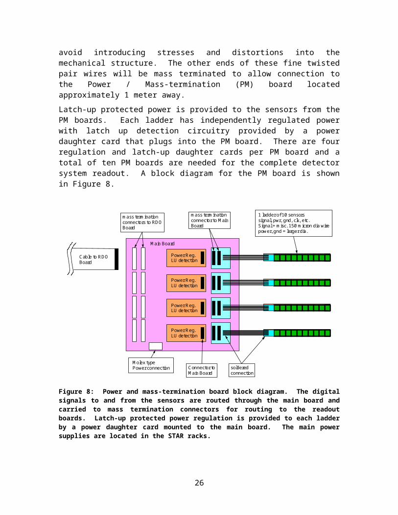
Mimostar-2 based telescope test at STARUsing a preliminary system design for analog readout, we have taken data with a set of Mimostar-2 sensors at STAR. This system is an early prototype whose performance is evaluated as part of the overall vertex detector development effort. We have successfully implemented a continuous readout 50 MHz data acquisition system with on-the-fly data sparsification that gives near three orders of magnitude data reduction from the raw ADC rates. This readout system has been mated with prototype Mimostar2 sensors and configured as a telescope system to measure the charged particle environment in the STAR environment near the final detector position. This telescope is shown in Figure 15.
28

Figure 15: Three Mimosrat-2 sensors in a telescope configuration used in a beam, test at STAR.
We find that the system works well, gives reasonable efficiency and accidental hit rates, and measures an angular distribution of tracks consistent with imaging the interaction diamond and with imaging beam-gas interaction type background. The prototype readout system integrated well into the existing STAR electronics and trigger infrastructure and functioned successfully as another STAR detector subsystem. This prototype readout system and the results obtained are described in a NIM paper1.
LVDS Data Path Readout TestAs a necessary part of the design validation, we have performed a test of the high speed LVDS data path. The
29

Figure 16: 200 MHz Data eye pattern measured at the RDO motherboard input to the FPGA (after all buffers) and triggered on the output data from the FPGA. Full width opening in system is ~ 2.3 ns.
4.2.5. Mechanical Design
Design OverviewThe mechanical design has been driven by the following design goals:
Minimize multiple coulomb scattering, particularly at the inner most layer
Locate the inner layer as close to the interaction region as possible
Allow rapid detector replacement
Provide complete spatial mapping of the pixels from the beginning
The first two goals, multiple coulomb scattering and minimum radius, set the limit on pointing accuracy to the vertex. This defines the efficiency of D and B mesons detection.
The third goal, rapid detector replacement, is motivated by recognition of difficulties encountered in previous experiments with unexpected detector failures. This third goal is also motivated by the need to replace detector that are radiation damaged from operating so close to the beam.
The fourth goal, complete spatial mapping, is important to achieve physics results in a timely fashion. The plan is to know at installation where the pixels are located with
30

respect to each other to within 20 microns and to maintain the positions throughout the operation.
The pixel detector (see fig. xx) consists of two concentric barrels of detector ladders 20 cm long. The inner barrel has a radius of 2.5 cm and the outer barrel has an 8 cm radius. The barrels separate into two halves for assembly and removal. In the installed location both barrel halves are supported with their own 3 point precision kinematic mounts located at one end close to the detector barrel. During installation, support is provided by the hinge structures mounted on a railed carriage. Cooling is provided by air flowing in from one end between the two barrel surfaces and returning in the opposite direction over the outer barrel surface and along the inner barrel surface next to the beam pipe.
Fig. xx Pixel detector mechanics showing detector barrel, support structures and insertion parts plus interface electronics boards.
The design of the components is presented first followed by mechanical and cooling analysis.
Detector ladder designAs previously mentioned (section xxx) the detector chips are arranged 10 in a row to form a ladder. An exploded view of the mechanical components is shown in Fig. xxx. The thinned silicon chips are bonded to a flex aluminum Kapton cable which is in turn bonded to a thin carbon composite structure. All electrical connections from the chips to
31

the cable are done with a single row of wire bonds along one edge of the ladder. The carbon composite sheet which is quite thin will only be sufficient for handling and heat conduction. The primary stiffness and support of the ladder is provided by the support beam. This particular ladder structure has not been built yet, but it will utilize construction methods that we have developed in our previous prototype designs[xxxx leo and gull wing protos]. Parts are aligned and held in place with vacuum chuck tooling for bonding. Fifty micron soft pressure sensitive acrylic adhesive [xxx reference 200MP by 3M] is used to make the bonds. A method has been developed which uses a 2xxx bar pressure chamber to remove bond voids and to stabilize the bond. The low elastic modulus of the adhesive is an important component in the design as it greatly reduces bi metal type deformations stemming from differential expansion caused by thermal changes and humidity changes. This will be discussed in more detail in the analysis section.
The next step in the ladder development will be to build mechanical prototypes the verify the mechanical design both structurally and thermally.
Fig. xxx Exploded view of the ladder showing components. The silicon is composed of 10 ~square chips, bit it is shown hear as continuous piece of silicon as it has been modeled for analysis.
Ladder support systemA critical part of the ladder support is the thin carbon composite beam which carries one inner ladder and three outer ladders as shown in Fig. xxxx. This beam which is an adaptation of the ALICE pixel detector design provides a very stiff support while minimizing the radiation length budget. Significant stiffness is required to control deformations from gravity, cooling air forces and differential expansion forces from both thermal and humidity variations. The composite beam carries a single inner ladder and three outer ladders. Ten of these modules form the two barrel layers. The beam in addition to its support function provides a duct for cooling air and adds cooling surface to increase heat transfer from the silicon chips. By making the beam from high strength and high thermal conductivity carbon fiber the wall thickness can be as thin as 200 microns and still satisfy strength and heat transfer requirements. The final thickness however, will probably be limited by fabrication challenges. Forming methods under consideration
32

are a single male mandrel with vacuum bagging or alternatively nested male and female mandrels.
Fig. xxxx Thin wall carbon support beam (green) carrying a single inner barrel ladder and three outer barrel ladders. The beam in addition to supporting the ladders provides a duct for conducting cooling air and added surface area to improve heat transfer to the cooling air.
The ladders will be glued to the beam using a low strength silicon adhesive as was done in the ATLAS pixel design. This adhesive permits rework replacement of single ladders.
Support of the beams with ladders is done in two halves with 5 sector beams per half module (see Fig xxxxx). The sector beams are attached to carbon composite “D tube” with precision dove tail mounts for easy assembly and replacement.
33
D- Tube sector beam

Fig. xxxxx Half module consisting of 5 sector beam modules. The sector beam modules are secured to a carbon composite D tube using a dove tail structure which permits easy replacement of sector modules. Carbon composite parts are shown in green for greater visibility.
The “D tube” supports the 5 sector beams and conducts cooling air to the sectors.
Kinematic support and docking mechanismWhen the pixel detector is in its final operating position it is secured at 3 points with precision reproducible kinematic mounts to the Inner Support Cylinder (ISC) as shown in Fig. xx6.
Fig. xx6 Detector assembly in the installed position supported with three kinematic mounts.
A more detailed view of the kinematic mounts is shown in Fig. xx7. The mounts provide a 3-2-1 constraint system which should allow repeatable installation to within a few microns.
34

Fig. xx7 Detailed view of the kinematic docking mounts for the pixel detector. The mounts provide a fully constrained support and operate with a spring loaded over center lock down.
Insertion mechanism and InstallationThe mechanics have been design for rapid installation and replacement. Instillation and removal of the pixel detector will be done from outside of the main STAR system with minimum disruption to other detectors systems. This will be done by assembling the two halves of the detector on either side of the beam pipe on rails outside of the STAR magnet iron. The detector carriage will be pushed into the center of STAR along the rails until it docks on the kinematic mounts. As shown in Figs. xx8 and xx9 the hinged support structure is guided by cam followers to track around the large diameter part of the beam pipe and close down at the center into the final operating position. Once the detector is docked in the kinematic mounts the hinged support from the carriage is decoupled allowing the kinematic mounts to carry the light weight detector system with a minimum of external forces affecting the position of the detector barrels. The external loads will be limited to the cables and the air cooling ducts. The cables are loosely bundled twisted pairs with xx micron conductors, so this load should be minimal. The two inch cooling ducts will be the greater load and may require additional design effort to isolate their effect so that the 20 micron position stability for the pixels can be maintained.
35

Fig. xx8 Track and cam guide system for inserting the detector.
Fig. xx9 Initially the detector halves have to be sufficiently open to clear the large diameter portion of the beam pipe. It then closes down sufficiently to fit inside the IFC while clearing the beam pipe supports and then finally it closes down to the final position with complete overlapping coverage of the barrels.
1 L. Greiner et al., “Results from a Prototype MAPS Sensor Telescope and Readout System with Zero Suppression for the Heavy Flavor Tracker at STAR” Nucl. Instr. Meth. A 589 (2008) 167.
pixel support hinges
cam followers and linear camslide rails
sliding carriage
Open Closed
36
Kinematic support
Cooling systemCooling of the detector ladders with pixel chips and drivers is done with forced air. The pixel chips dissipate a total of 160 watts or 100 mW/cm2 and an additional 80 watts is required for the drivers. In addition to the ladder total of 240 watts some fraction of this is required for voltage regulators and latch up electronics that are off the ladder but reside in the air cooled volume. The temperature of operation is still under consideration. An optimum temperature for the detectors is around 0 deg C, but they can be operated at 34 deg C without too much noise degradation. The cooling system design is simplified if we can operate at 24 deg C, slightly above the STAR hall temperature, however if the cooler temperature is required the cooling system will be equipped with thermal isolation and condensation control when the system is shut down. In any case the design will include humidity and temperature control as well as filtration. Cooling studies (see section xxx) show that air velocities of 8 m/s are required over the detector surfaces and a total flow rate of 200 cfpm is sufficient to maintain silicon temperatures of less than 20 deg C above the air temperature.
The detector cooling path is shown in Fig. xx10. Air is pumped in through the support beam. A baffle in the ISC forces the air to return back over the detector surfaces both along the beam pipe and along the ISC.
Fig. xx10 Pixel detector cooling air path. The air flows down the center of the sector modules and returns back over the detector ladders on the sector modules and into the larger ISC volume where it is ducted back to the air cooling unit.
The air chiller system providing the cooling air circulating through the pixel detector has not been completely specified yet, but sizing and ducting have been investigated for a system (see Fig. xx11) with 400 cfpm capacity (twice currently expected requirement). A commercially available centrifugal pump with a 5 horsepower motor is sufficient for this system. It is expected that the chiller would be located in the wide angle hall within
37

50 ft of the pixel enclosure and would be connected with 6 inch flexible ducts. An estimate of the required chiller heat capacity is given in Table xx1.
Internal duct 2 in diameter X 5 ft
Internal duct 2 in diameter X 5 ft
external duct 6 in diameter X 50 ft
external duct 6 in diameter X 50 ft
chiller
pump
Wide angle hall ISC
Air flow: 400 SCFM
Total pressure drop: 22 inches water
Fig. xx11 Schematic outline of air cooling system for the pixel detector
Heat source Power (watts)
detector silicon 160
on ladder signal drivers 80
voltage regulators in ISC 24
heat influx through ducting and ISC if 35 deg C below ambient
600 - 2000
pumping 1000
Total load on chiller 1900 - 3300
Table xx1 Preliminary estimate of heat load on the chiller for the pixel air cooling system
Cabling and Service systemThe required wiring connections are identified in Fig. 6 (xx this is Leo’s section). The 2 m fine wire twisted pair (pair diameter .32 mm) bundles leading from the ladders to the interface cards are designed to minimize mass, space and mechanical coupling forces that could disturb the pixel positions. The space envelope required for these bundles is illustrated in Fig. xx12.
38

Fig. xx12 Cable bundle envelope for ladder connections. The blue pairs include 40 signal pairs, clock and trigger lines and JTAG communication. The red conductors are power.
There will be a 2’X2’X3’ crate for the readout boards. This must be located outside of the main magnetic field and outside of the highest particle flux region. To achieve the required data transfer rates the LVDS signal cables running between this crate and drivers inside the ISC are limited to 6 meters. To meet these constraints the readout crate will a be located on the floor at the end of the magnet pole tip, since all the space on the outside of the pole tip iron is fully occupied with other detector systems. The crate will be portable on wheels to accommodate end cap access requirements. Compared to the cables running to the detector the power and fiber optic cables from the readout crate to the outside are relatively small and provide little handling burden.Installation
Alignment and spatial mappingThe pixel system is being designed to have full pixel to pixel spatial mapping at installation with a 3D tolerance envelope of 20 microns. This will eliminate the need for spatial calibration with tracking other than determining the 6 parameters defining the pixel detector unit location relative to the outer tracking detectors. Tracking, however, can used with the pixel detector to spatially map the outer detectors if required.
The mapping and alignment will be done by using a vision coordinate machine to determine the detector locations on the fully constructed 20 ladder half modules. The
39

half modules will then be installed in STAR without disturbing the relative positions of the pixels.
Addressing this in more detail, a support fixture for the half modules will be used in the vision coordinate machine which has kinematic mounts identical to the kinematic mounts in the ISC for securing the half module. The pixel chips will be manufactured with reference targets in the top metal layer that can be picked up by the vision coordinate machine and the ladders will be mounted such that there is an unobstructed view. The fixture will be rotated for each ladder measurement. Full 3D measurements of the chips on the ladder are required since the ladder flatness will lie outside of the 20 micron envelope. The fixture will have precision reference targets on each ladder plane so that the ladder points can be tied together into a single coordinate frame. The map of the fixture targets can be measured once with a touch probe measuring machine thus avoiding extreme machining tolerance requirements for the fixture. Precision machining, however, will be required, for the kinematic mounts and their placement tool.
For this approach to work the ladders must hold to their mapped position within 20 microns independent of changes in temperature, humidity and gravity direction.
The detector ladders have 1 mm overlapping active regions with their neighbors, so a check of the mapping accuracy will be done with tracking.
Mechanical Design Simulation and Prototyping
Ladder support Structural analysis
Ladder support prototype development
Ladder cooling analysis
Ladder cooling prototype tests
Insertion prototype tests
40

Kinematic support tests
41

4.3. IST
42

4.4. SSD
4.4.1. SSD Upgrade Design
Silicon description
Digitization of the data at the end of the ladder
Slow Controls
Power
DAQ1000
Cooling
4.4.2. SSD Upgrade
Current status
Refurbishing silicon
Upgrade for readout electronics
Design of cooling system
LV and Power
Slow controls
Incorporation into DAQ1000 data stream
Cable Design
43

4.4.3. Integration Issues
Resources for integration
Alignment mounts on the Cone
Cable paths on the cone
Space allocation
Interface with the FGT
Design responsibilities for cables on the cone
Cable breakout out at the cone boundaryPower (LV, Bias, feedback)
Data fibers
Slow Control
Location of the RDO BoxEnd of Magnet or
Platform
Space on the PlatformCables from cone to the platform
Rack space
44

Cooling
Triggering
4.4.4. Staging Plan
Three ladder prototype test
Installation of full detector
4.4.5. Institutional Responsibilities
Management structure
STAR commitmentResources required
Cooling engineer
Slow control software implementer
Digital designer to incorporate slow controls into fiber optical path used for data
Electronic engineering for readout upgrade
BNL
LBNL
Software responsibility
Other collaboration contributed resources
HFT responsibilities for interface
45

4.5. Integration into STAR
4.5.1. Mechanical AssemblyCone and support Structure
Overview
West-East Cone
ICS
OCS
Assembly procedure
Assembly area requirements
4.5.2. Beam Pipe
Mechanical
Bakeout Considerations
Support
4.5.3. Services
Summary of Air, Water and Power
Space requirements on Magnet and PlatformData Acquisition
4.5.4. Controls
4.5.5. Data Acquisition
46

4.5.6. SSD
47

4.6. Software
48

4.7. Cost and Schedule
49

5. Resources
50

1. Appendix 1
5.1. Description of the Pixel RDO SystemThis document is an extension of the Pixel RDO addendum to the HFT proposal. It is intended to give detailed parameters of the function of the Pixel readout system that will allow for the understanding of the logic and memory and requirements and the functionality of the readout system. We will present the designs of the Phase-1 and Ultimate readout systems under periodic triggering conditions. The simulation of the system response to random triggering of the type expected to be seen at the STAR experiment is ongoing and will be available upon completion. The readout design is highly parallel and one of the ten parallel readout systems is analyzed for each system.
5.1.1. Phase-1 Readout ChainThe Phase-1 detector will consist of two carrier assemblies, each containing four ladders with ten sensors per ladder. The readout is via parallel identical chains of readout electronics. The relevant parameters from the RDO addendum are reproduced in Table 5.
Item Number
Bits/address 20
Integration time 640 µs
Hits / frame on Inner sensors (r=2.5 cm) 295
Hits / frame on Outer sensors (r=8.0 cm) 29
Phase-1 sensors (Inner ladders) 100
Phase-1 sensors (Outer ladders) 300
Event format overhead TBD
Average Pixels / Cluster 2.5
Table 5: Parameters for the Phase-1 based detector system used in the example calculations shown below.
The functional schematic of the system under discussion is presented in Figure 17.
51
AddressCounter(zero-
suppression)
EventBuffer
EventBuffer
EventBuffer
1
2
10
EventBuilder
RDOBuffer
SIU
DAQPC
Disk
160 MHzBinary Data
(4 chains per sensor) * (10 sensors per ladder) *(4 ladders per RDO board) = 160 chains per RDO board
160 independent sensor data chains
One per RDO board
FPGA Block RAM
Figure 17: Functional schematic diagram for one Phase-1 sensor based RDO board. Each RDO board services one inner ladder and 3 outer ladders. Each ladder contains 10 sensors.
We will show the system function for two cases. The first is for a periodic trigger rate of 1 kHz. The second is for a periodic trigger rate of 2 kHz. These cases make the scaling clear. In both cases we will use the average (pile-up included) event size. We are currently simulating the dynamic response of the system to the triggering and event size fluctuations seen at STAR and will make this information available after the simulations are completed. It is important to note that the system is FPGA based and can be easily reconfigured to maximize the performance by the adjustment of buffer sizes, memory allocations, and most other parameters. The relevant parameters of the system pictured above are described below;
Data transfer into event buffers – The binary hit data is presented to the address counter at 160 MHz. The corresponding hit address data from the adders counter is read synchronously into the event buffers for one full frame of a 640 × 640 sensor at 160 MHz. This corresponds to an event buffer enable time of 640 µs.
Event Buffers – Each sensor output is connected to a block of memory in the FPGA which serves as the storage for the event buffers. Each block of memory is configured as dual ported RAM and. The overall FPGA block RAM used per sensor output is sized to allow for storage of up to ten average events with event size fluctuation. This leads to a total buffer size that is 20 × the size required for the average sized event (different for inner and outer sensors). The FPGA block RAM will be configured with pointer based
52

memory management to allow for efficient utilization of the RAM resources. The average inner sensor has 295 hits / event. There are 4 outputs per sensor so the average inner sensor event address length is (0.25 sensor area) × (295 hits) × (20 bits) × (2 factor for event size fluctuations) × (2.5 hits per cluster) = 7,375 bits. Multiplying this event buffer size by 10 gives the size of the RAM required for the full set of event buffers required. The event buffer block RAM size for each inner sensor output is 73,750 bits or 3,688 20-bit addresses.
For outer sensors, the event buffer size is calculated similarly. The average outer sensor has 29 hits / event. There are 4 outputs per sensor so the average inner sensor event address length is (0.25 sensor area) × (29 hits) × (20 bits) × (2 factor for event size fluctuations) × (2.5 hits per cluster) = 725 bits. Multiplying this event buffer size by 10 gives the size of the RAM required for the full set of event buffers required. The event buffer block RAM size for each outer sensor output is 7250 bits or 363 20-bit addresses.
Data transfer into the RDO buffer via the event builder – This process is internal to the FPGA, does not require computational resources, and can run at high speed. In the interests of simplicity, we will assume a 160 MHz clock to move data in 20-bit wide address words. The event builder first adds a 128 Byte header that contains the trigger ID and other identifying information into the RDO buffer, and then moves the address data from the event buffers into the RDO buffer in 20-bit words. The average carrier event size is [(29 hits / sensor (outer)) × (10 sensors) × (3 ladders) + (295 hits / sensor (inner)) × (10 sensors) × (1 ladders)] × (2.5 hits / cluster) = 9550 address words (20-bit). The RDO buffer is 5 × the size required for an average event and is thus 955 kb in size. The full time required to transfer the address data into the RDO buffer (in 20-bit per clock transfers) is then 59.7 µs.
Data transfer from the RDO buffer over the DDL link – The RDO buffer is dual-ported and thus readout from the SIU to the RORC can proceed as soon as the RDO buffer begins filling. The data transfer rates for the SIU – RORC combination as a function of fragment size are shown in Figure 18.
53

Figure 18: Bandwidth of a single channel of the SIU - RORC fiber optic link as a function of event fragment size with an internal and external (DDL) data source using two D-RORC channels. From the LECC 2004 Workshop in Boston.
In this case, we will assume that we are padding the 20-bit address data to 32-bit word lengths for DDL transfer. The event size is then (32 bits) × (9550 address words) = 305.6 kb or 38.2 kB. In this example, our transfer rate is ~ 200 MB / s. This transfer then takes 191 µs.
Data transfer to the STAR DAQ for event building – The event data is buffered in the DAQ PC RAM (>4GB) until only accepted events are written to disk and then transferred via Ethernet to an event building node of the DAQ system. Level 2 trigger accepts are delivered to the RDO system and transferred via the SIU – RORC to the DAQ receiver PCs. Only the events that have been accepted by level 2 are then built into an event. In this way, the buffer provided by the DAQ PC RAM provides for the elasticity needed for an average event acceptance of 1 kHz
The results of these calculations and discussion are presented below in the chronograms in Figure 19 and Figure 20.
54
Event Buffer #1
RDO Buffer
SIU
640 us
Event Buffer #2
Event Buffer #3
Event Buffer #4
Event Builder
Trigger @ 1 kHz
640 us 640 us
1 2 3 4
Figure 19: Chronogram of the Phase-1 based readout system functions for a 1 kHz periodic trigger.
640 usEvent Buffer #1
RDO Buffer
SIU
Event Buffer #2
Event Buffer #3
Event Buffer #4
Event Builder
Trigger @ 2 kHz
640 us 640 us
1 2 3 4 5 6 7
640 us 640 us 640 us
Figure 20: Chronogram of the Phase-1 based readout system functions for a 2 kHz periodic trigger.
The memory resources required in the FPGA / motherboard combination for this readout design are (120 outer sensor readout buffers) × (7.25 kb per event buffer) + (262.5 kb for the RDO buffer) + (40 inner sensor readout buffers) × (73.75 kb per event buffer) + (955 kb for the RDO buffer)= 4775 kb. The Xilinx Virtex-5 FPGA used in our design
55

contains 4.6 – 10.4 Mb of block RAM so the entire design should fit easily into the FPGA.
Ultimate Sensor Detector Readout Chain
Again, the Ultimate sensor readout system consists of ten parallel readout chains. The main difference between the Phase-1 sensors and the Ultimate sensors is the inclusion of zero suppression circuitry in the Ultimate sensor, thus only addresses are read out into the RDO boards. In addition, the integration time of the Ultimate sensor is 200 µs and there is one data output per sensor. These differences lead to the functional schematic of the readout system shown in Figure 21.
FPGA Block RAM
EventBuffer
EventBuffer
EventBuffer
1
2
10
EventBuilder
RDOBuffer
SIU
DAQPC
Disk
160 MHz Address only data
(1 chain per sensor) * (10 sensors per ladder) *(4 ladders per RDO board) = 40 chains per RDO board
40 independent sensor data chains
One per RDO board
Figure 21: Functional schematic diagram for one Ultimate sensor based RDO board. Each RDO board services one inner ladder and 3 outer ladders. Each ladder contains 10 sensors.
We will show the system function for the same two cases as shown for the Phase-1 readout system. The first is for a periodic trigger rate of 1 kHz. The second is for a periodic data rate of 2 kHz. Again, in both cases we will use the average (pile-up included) event size. The relevant parameters of the Ultimate sensor based system pictured above are described in Table 6.
56

Item N umber
Bits/address 20
Integration time 200 µs
Hits / frame on Inner sensors (r=2.5 cm) 246
Hits / frame on Outer sensors (r=8.0 cm) 24
Ultimate sensors (Inner ladders) 100
Ultimate sensors (Outer ladders) 300
Event format overhead TBD
Average Pixels / Cluster 2.5
Average Trigger rate 1 kHz
Table 6: Parameters for the Ultimate sensor based detector system used in the example calculations shown below.
Data transfer into event buffers – The 20-bitaddress data is presented to the event buffer 160 MHz. The integration time is now 200 µs giving an event buffer enable time of 200 µs.
Event Buffers – Again, we will calculate the amount of FPGA block RAM required for the event buffering. The average inner sensor has 246 hits / event. There are 4 outputs per sensor so the average inner sensor event address length is (0.25 sensor area) × (246 hits) × (20 bits) × (2 factor for event size fluctuations) × (2.5 hits per cluster) = 6150 bits. Multiplying this event buffer size by 10 gives the size of the RAM required for the full set of event buffers required. The event buffer block RAM size for each inner sensor output is 61,500 bits or 3,075 20-bit addresses.
For outer sensors, the event buffer size is calculated similarly. The average outer sensor has 24 hits / event. There are 4 outputs per sensor so the average inner sensor event address length is (0.25 sensor area) × (24 hits) × (20 bits) × (2 factor for event size fluctuations) × (2.5 hits per cluster) = 600 bits. Multiplying this event buffer size by 10 gives the size of the RAM required for the full set of event buffers required. The event buffer block RAM size for each outer sensor output is 6000 bits or 300 20-bit addresses.
Data transfer into the RDO buffer via the event builder –We will again assume a 160 MHz clock to move data in 20-bit wide address words. The event builder first adds a 128 Byte header that contains the trigger ID and other identifying information into the RDO buffer, and then moves the address data from the event buffers into the RDO buffer in 20-bit words. The average carrier event size is [(24 hits / sensor (outer)) × (10 sensors) × (3 ladders) + (246 hits / sensor (inner)) × (10 sensors) × (1 ladders)] × (2.5 hits / cluster) = 7950 address words (20-bit). The RDO buffer is 5 × the size required for an average event and is thus 795 kb in size. The full time required to transfer the address data into the RDO buffer (in 20-bit per clock transfers) is then 49.7 µs.
57

Data transfer from the RDO buffer over the DDL link – The RDO buffer is dual-ported and thus readout from the SIU to the RORC can proceed as soon as the RDO buffer begins filling. Again, we will assume that we are padding the 20-bit address data to 32-bit word lengths for DDL transfer. The event size is then (32 bits) × (7950 address words) = 254.4 kb or 31.8 kB. In this example, our transfer rate is ~ 200 MB / s. This transfer then takes 159 µs.
Data transfer to the STAR DAQ for event building – Again, only the events that have been accepted by level 2 are then built into an event. In this way, the buffer provided by the DAQ PC RAM provides for the elasticity needed for an average event acceptance of 1 kHz
The results of these calculations and discussion are presented below in the chronograms in Figure 22 and Figure 23.
Event Buffer #1
RDO Buffer
SIU
Event Buffer #2
Event Buffer #3
Event Buffer #4
Event Builder
Trigger @ 1 kHz
1 2 3 4
200 us 200 us200 us
Figure 22: Chronogram of the Ultimate sensor based readout system functions for a 1 kHz periodic trigger.
58

Event Buffer #1
RDO Buffer
SIU
Event Buffer #2
Event Buffer #3
Event Buffer #4
Event Builder
Trigger @ 2 kHz
1 2 3 4 5 6 7
200 us 200 us 200 us 200 us 200 us
Figure 23: Chronogram of the Ultimate sensor based readout system functions for a 2 kHz periodic trigger.
The system memory resource requirements are somewhat less than those required for the Phase-1 RDO system. This fits easily into the memory resources of the Virtex-5 FPGA.
59

References
60