high-current low dropout regulators
TRANSCRIPT

2016-2019 Microchip Technology Inc. DS20005685B-page 1
MIC2915X/30X/50X/75X
Features
• High Current Capability:
- MIC29150/29151/29152/29153: 1.5A
- MIC29300/29301/29302/29303: 3A
- MIC29500/29501/29502/29503: 5A
- MIC29751/29752: 7.5A
• Low Dropout Voltage
• Low Ground Current
• Accurate 1% Guaranteed Tolerance
• Extremely Fast Transient Response
• Reverse-Battery and “Load Dump” Protection
• Zero-Current Shutdown Mode (5-Pin Versions)
• Error Flag Signals Output Out-of-Regulation (5-Pin Versions)
• Also Characterized for Smaller Loads with Industry-Leading Performance Specifications
• Fixed-Voltage and Adjustable Versions
Applications• Battery-Powered Equipment
• High-Efficiency Green Computer Systems
• Automotive Electronics
• High-Efficiency Linear Power Supplies
• High-Efficiency Post-Regulator for Switching Supply
General Description
The MIC2915x/2930x/2950x/2975x are high current,high accuracy, low dropout voltage regulators. UsingMicrochip’s proprietary Super βeta PNP process with aPNP pass element, these regulators feature 350 mV to425 mV (full load) typical dropout voltages and very lowground current. Designed for high current loads, thesedevices also find applications in lower current,extremely low dropout-critical systems, where their tinydropout voltage and ground current values areimportant attributes.
The MIC2915x/2930x/2950x/2975x are fully protectedagainst overcurrent faults, reversed input polarity,reversed lead insertion, overtemperature operation,and positive and negative transient voltage spikes. Fivepin fixed-voltage versions feature logic level ON/OFFcontrol and an error flag that signals whenever theoutput falls out of regulation. Flagged states includelow input voltage (dropout), output current limit,overtemperature shutdown, and extremely high voltagespikes on the input.
On the MIC29xx1 and MIC29xx2, the ENABLE pin maybe tied to VIN if it is not required for ON/OFF control.The MIC2915x/2930x/2950x are available in 3-pin and5-pin TO-220 and surface mount TO-263 (D2Pak)packages. The MIC2975x 7.5A regulators are availablein a 5-pin TO-247 package. The 1.5A, adjustable outputMIC29152 is available in a 5-pin power D-Pak(TO-252) package.
For applications with input voltage 6V or below, seeMIC37xxx LDOs.
Package Types
MIC29150/300/5003-Lead TO-220 (T)
(Top View)
TAB
3 OUT
2 GND
1 IN
TAB 3 GND
4 OUT5 FLG
2 IN1 EN
MIC29151/301/501/7515-Lead TO-220 Fixed Voltage (T)
(Top View)
High-Current Low Dropout Regulators

MIC2915X/30X/50X/75X
DS20005685B-page 2 2016-2019 Microchip Technology Inc.
Package Types (Continued)
MIC29152/302/5025-Lead TO-220 Adjustable Voltage (T)
(Top View)
TAB 3 GND
4 OUT5 ADJ
2 IN1 EN
TAB 3 GND
4 OUT5 ADJ
2 IN1 FLG
MIC29153/303/5035-Lead TO-220 Adjustable with Flag (T)
(Top View)
12345
ENINGNDOUTFLG
MIC297515-Lead TO-247 Fixed Voltage (WT)
(Top View)
12345
ENINGNDOUTADJ
MIC297525-Lead TO-247 Adjustable Voltage (WT)
(Top View)TA
B
3 OUT
2 GND
1 IN
MIC29150/3003-Lead TO-263 (D2Pak) (UT)
(Top View)
TAB
5 FLG4 OUT3 GND2 IN1 EN
MIC29151/301/5015-Lead TO-263 (D2Pak) Fixed Voltage (U)
(Top View)
TAB
5 ADJ4 OUT3 GND2 IN1 EN
MIC29302/5025-Lead TO-263 (D2Pak) Adj. Voltage (U)
(Top View)
TAB
5 ADJ4 OUT3 GND2 IN1 FLG
MIC29153/303/5035-Lead TO-263 (D2Pak) Adj. with Flag (U)
(Top View)
1 EN2 IN3 GND4 OUT5 ADJ
MIC291525-Lead TO-252 (D-Pak) Adjustable Voltage (D)
(Top View)

2016-2019 Microchip Technology Inc. DS20005685B-page 3
MIC2915X/30X/50X/75X
Typical Application Circuits
Functional Diagram
MIC29300-3.3
10μF Tantalum
3.3V @ 3AIN OUT
GND
CIN
5V OUTIN
ADJGND
EN10μF Tantalum
*R1
*R2
CIN+
MIC29300Fixed Output Version
MIC29152Adjustable Output Version
* See Minimum Load Current Section
1.180V 1.240VREFERENCE
IN
FLAG
ENTHERMAL
SHUT-DOWN
OUT
ADJ†
GND
R1*
R2*
O.V.I LIMIT
32V
* FEEDBACK NETWORK IN FIXED VERSIONS ONLY† ADJUSTABLE VERSION ONLY

MIC2915X/30X/50X/75X
DS20005685B-page 4 2016-2019 Microchip Technology Inc.
1.0 ELECTRICAL CHARACTERISTICS
Absolute Maximum Ratings † (Note 1)
Input Supply Voltage (VIN) (Note 1)............................................................................................................. –20V to +60VEnable Input Voltage (VEN) ........................................................................................................................... –0.3V to VINPower Dissipation................................................................................................................................... Internally LimitedESD Rating ............................................................................................................................................................ Note 2
Operating Ratings‡
Maximum Operating Input Voltage............................................................................................................................+26V
† Notice: Stresses above those listed under “Absolute Maximum Ratings” may cause permanent damage to the device.This is a stress rating only and functional operation of the device at those or any other conditions above those indicatedin the operational sections of this specification is not intended. Exposure to maximum rating conditions for extendedperiods may affect device reliability.
‡ Notice: The device is not guaranteed to function outside its operating ratings.
Note 1: Maximum positive supply voltage of 60V must be of limited duration (<100 ms) and duty cycle (≤1%). Themaximum continuous supply voltage is 26V. Exceeding the absolute maximum rating may damage thedevice.
2: Devices are ESD sensitive. Handling precautions recommended.

2016-2019 Microchip Technology Inc. DS20005685B-page 5
MIC2915X/30X/50X/75X
TABLE 1-1: ELECTRICAL CHARACTERISTICS (Note 1, Note 2)
Electrical Characteristics: VIN = VOUT + 1V; IOUT = 10 mA; TJ = +25°C. Bold values indicate –40°C ≤ TJ ≤ +125°C, unless noted.
Parameter Symbol Min. Typ. Max. Units Conditions
Output Voltage VOUT
–1 — 1%
IOUT = 10 mA
–2 — 210 mA ≤ IOUT ≤ IFL, (VOUT + 1V) ≤ VIN ≤26V (Note 3)
Line Regulation — 0.06 0.5 % IOUT = 10 mA, (VOUT + 1V) ≤ VIN ≤ 26V
Load Regulation — 0.2 1 %VIN = VOUT + 1V, 10 mA ≤ IOUT ≤ 1.5A (Note 3, Note 4)
∆VO/∆T — 20 100 ppm/°COutput Voltage (Note 4) Temperature Coefficient
Dropout Voltage∆VOUT = –1% (Note 5)
— 80 200
mV
MIC2915x IOUT = 100 mA
— 220 — MIC2915x IOUT = 750 mA
— 350 600 MIC2915x IOUT = 1.5A
— 80 175 MIC2930x IOUT = 100 mA
— 250 — MIC2930x IOUT = 1.5A
— 370 600 MIC2930x IOUT = 3A
— 125 250 MIC2950x IOUT = 250 mA
— 250 — MIC2950x IOUT = 2.5A
— 370 600 MIC2950x IOUT = 5A
— 80 200 MIC2975x IOUT = 250 mA
— 270 — MIC2975x IOUT = 4A
— 425 750 MIC2975x IOUT = 7.5A
Ground Current (Note 6) IGND
— 8 20
mA
MIC2915x IOUT = 750 mA, VIN = VOUT + 1V
— 22 — MIC2915x IOUT = 1.5A
— 10 35MIC2930x IOUT = 1.5A, VIN = VOUT + 1V
— 37 — MIC2930x IOUT = 3A
— 15 50MIC2950x IOUT = 2.5A, VIN = VOUT + 1V
— 70 — MIC2950x IOUT = 5A
— 35 75MIC2975x IOUT = 4A, VIN = VOUT + 1V
120 — MIC2975x IOUT = 7.5A
Ground Pin Current at Dropout
IGRNDDO
— 0.9 —
mA
MIC2915x, VIN = 0.5V less than specified VOUT × IOUT = 10 mA
— 1.7 —MIC2930x, VIN = 0.5V less than specified VOUT × IOUT = 10 mA
— 2.1 —MIC2950x, VIN = 0.5V less than specified VOUT × IOUT = 10 mA
— 3.1 —MIC2975x, VIN = 0.5V less than specified VOUT × IOUT = 10 mA
Current Limit ILIM
— 2.1 3.5
A
MIC2915x, VOUT = 0V, (Note 7)
— 4.5 5.0 MIC2930x, VOUT = 0V, (Note 7)
— 7.5 10.0 MIC2950x, VOUT = 0V, (Note 7)
— 9.5 15.0 MIC2975x, VOUT = 0V, (Note 7)

MIC2915X/30X/50X/75X
DS20005685B-page 6 2016-2019 Microchip Technology Inc.
en, Output Noise Voltage (10 Hz to 100 kHz)IL = 100 mA
— 400 —µVRMS
CL = 10 µF
— 260 — CL = 33 µF
Ground Current in Shutdown
— 2 10µA
MIC29150/1/2/3 only
— — 30 VEN = 0.4V
Reference - MIC29xx2/MIC29xx3
Reference Voltage1.228 1.240 1.252 V
—1.215 — 1.265 VMAX
Reference Voltage 1.203 — 1.277 V Note 8
Adjust Pin Bias Current— 40 80
nA —— — 120
Reference Voltage Temperature Coefficient
— 20 — ppm/°C Note 9
Adjust Pin Bias Current Temperature Coefficient
— 0.1 — nA/°C —
Flag Output (Error Comparator) - MIC29xx1/29xx3
Output Leakage Current— 0.01 1.00
µA VOH = 26V— — 2.00
Output Low Voltage VOL— 220 300
mVDevice set for 5V, VIN = 4.5VIOL = 250 µA— — 400
Upper Threshold Voltage40 60 —
mV Device set for 5V, (Note 10)25 — —
Lower Threshold Voltage— 75 95
mV Device set for 5V, (Note 10)— — 140
Hysteresis — 15 — mV Device set for 5V, (Note 10)
TABLE 1-1: ELECTRICAL CHARACTERISTICS (Note 1, Note 2) (CONTINUED)
Electrical Characteristics: VIN = VOUT + 1V; IOUT = 10 mA; TJ = +25°C. Bold values indicate –40°C ≤ TJ ≤ +125°C, unless noted.
Parameter Symbol Min. Typ. Max. Units Conditions

2016-2019 Microchip Technology Inc. DS20005685B-page 7
MIC2915X/30X/50X/75X
ENABLE Input - MIC29xx1/MIC29xx2
Input Logic Voltage Low (OFF)
— — 0.8 V —
Input Logic Voltage High (ON)
2.4 — — V —
Enable Pin Input Current
— 100 600
µA
VEN = 26V— — 750
0.7 — 2VEN = 0.8V
— — 4
Regulator Output Current in Shutdown
— 10 500 µA VEN ≤ 0.8V and VIN ≤ 26V, VOUT = 0.
Note 1: Specification for packaged product only.
2: When used in dual supply systems where the regulator load is returned to a negative supply, the output voltage must be diode clamped to ground.
3: Full load current (IFL) is defined as 1.5A for the MIC2915x, 3A for the MIC2930x, 5A for the MIC2950x, and 7.5A for the MIC2975x families.
4: Output voltage temperature coefficient is defined as the worst case voltage change divided by the total temperature range.
5: Dropout voltage is defined as the input-to-output differential when the output voltage drops to 99% of its normal value with VOUT + 1V applied to VIN.
6: Ground pin current is the regulator quiescent current. The total current drawn from the source is the sum of the load current plus the ground pin current.
7: VIN = VOUT (nominal) + 1V. For example, use VIN = 4.3V for a 3.3V regulator or use 6V for a 5V regulator. Employ pulse-testing procedures to pin current.
8: VREF ≤ VOUT ≤ (VIN – 1V), 2.3V ≤ VIN ≤ 26V, 10 mA < IL ≤ IFL, TJ ≤ TJMAX.
9: Thermal regulation is defined as the change in output voltage at a time T after a change in power dissipa-tion is applied, excluding load or line regulation effects. Specifications are for a 200 mA load pulse at VIN = 20V (a 4W pulse) for T = 10 ms.
10: Comparator thresholds are expressed in terms of a voltage differential at the adjust terminal below the nominal reference voltage measured at 6V input. To express these thresholds in terms of output voltage change, multiply by the error amplifier gain = VOUT/VREF = (R1 + R2)/R2. For example, at a programmed output voltage of 5V, the error output is guaranteed to go low when the output drops by 95 mV x 5V/1.240V = 384 mV. Thresholds remain constant as a percent of VOUT as VOUT is varied, with the drop-out warning occurring at typically 5% below nominal, 7.7% guaranteed.
TABLE 1-1: ELECTRICAL CHARACTERISTICS (Note 1, Note 2) (CONTINUED)
Electrical Characteristics: VIN = VOUT + 1V; IOUT = 10 mA; TJ = +25°C. Bold values indicate –40°C ≤ TJ ≤ +125°C, unless noted.
Parameter Symbol Min. Typ. Max. Units Conditions

MIC2915X/30X/50X/75X
DS20005685B-page 8 2016-2019 Microchip Technology Inc.
TEMPERATURE SPECIFICATIONS (Note 1)
Parameters Sym. Min. Typ. Max. Units Conditions
Temperature Ranges
Storage Temperature Range TS –65 — +150 °C —
Operating Junction Temperature TJ –40 — +125 °C —
Lead Temperature — — — +260 °C Soldering, 5 sec.
Package Thermal Resistance
Thermal Resistance TO-220 θJC — 2 — °C/W —
Thermal Resistance TO-263 θJC — 2 — °C/W —
Thermal Resistance TO-247 θJC — 1.5 — °C/W —
Thermal Resistance TO-252 θJC — 3 — °C/W —
Thermal Resistance TO-252 θJA — 56 — °C/W —
Note 1: The maximum allowable power dissipation is a function of ambient temperature, the maximum allowable junction temperature and the thermal resistance from junction to air (i.e., TA, TJ, JA). Exceeding the maximum allowable power dissipation will cause the device operating junction temperature to exceed the maximum +125°C rating. Sustained junction temperatures above +125°C can impact the device reliability.

2016-2019 Microchip Technology Inc. DS20005685B-page 9
MIC2915X/30X/50X/75X
2.0 TYPICAL PERFORMANCE CURVES
FIGURE 2-1: MIC2915x Dropout Voltage vs. Output Current.
FIGURE 2-2: MIC2915x Dropout Voltage vs. Temperature.
FIGURE 2-3: MIC29150-5.0 Dropout Characteristics.
FIGURE 2-4: MIC2915x Ground Current vs. Output Current.
FIGURE 2-5: MIC2915x Ground Current vs. Supply Voltage.
FIGURE 2-6: MIC2915x Ground Current vs. Supply Voltage.
Note: The graphs and tables provided following this note are a statistical summary based on a limited number ofsamples and are provided for informational purposes only. The performance characteristics listed hereinare not tested or guaranteed. In some graphs or tables, the data presented may be outside the specifiedoperating range (e.g., outside specified power supply range) and therefore outside the warranted range.

MIC2915X/30X/50X/75X
DS20005685B-page 10 2016-2019 Microchip Technology Inc.
FIGURE 2-7: MIC2915x Ground Current vs. Temperature.
FIGURE 2-8: MIC2915x Ground Current vs. Temperature.
FIGURE 2-9: MIC2915x Ground Current vs. Temperature.
FIGURE 2-10: MIC29150-3.3 Output Voltage vs. Temperature.
FIGURE 2-11: MIC29150-3.3 Short-Circuit Current vs. Temperature.
FIGURE 2-12: MIC2915x Ground Current vs. Input Voltage.

2016-2019 Microchip Technology Inc. DS20005685B-page 11
MIC2915X/30X/50X/75X
FIGURE 2-13: MIC29151-xx/2 Enable Current vs. Temperature.
FIGURE 2-14: MIC2915x Load Transient.
FIGURE 2-15: MIC2915x Load Transient.
FIGURE 2-16: MIC29152/3 Adjust Pin Current vs. Temperature.
FIGURE 2-17: MIC2915x Line Transient.
FIGURE 2-18: MIC2915x Line Transient.

MIC2915X/30X/50X/75X
DS20005685B-page 12 2016-2019 Microchip Technology Inc.
FIGURE 2-19: MIC2915x Output Impedance vs. Frequency.
FIGURE 2-20: MIC29152 Ground Current vs. Temperature.
FIGURE 2-21: MIC29152 Dropout Voltage vs. Output Current.
FIGURE 2-22: MIC2930x Dropout Voltage vs. Output Current.
FIGURE 2-23: MIC2930x Dropout Voltage vs. Temperature.
FIGURE 2-24: MIC29300-3.3 Dropout Characteristics.

2016-2019 Microchip Technology Inc. DS20005685B-page 13
MIC2915X/30X/50X/75X
FIGURE 2-25: MIC2930x Ground Current vs. Output Current.
FIGURE 2-26: MIC2930x Ground Current vs. Supply Voltage.
FIGURE 2-27: MIC2930x Ground Current vs. Supply Voltage.
FIGURE 2-28: MIC2930x Ground Current vs. Temperature.
FIGURE 2-29: MIC2930x Ground Current vs. Temperature.
FIGURE 2-30: MIC2930x Ground Current vs. Temperature.

MIC2915X/30X/50X/75X
DS20005685B-page 14 2016-2019 Microchip Technology Inc.
FIGURE 2-31: MIC29300-3.3 Output Voltage vs. Temperature.
FIGURE 2-32: MIC29300-5.0 Short-Circuit Current vs. Temperature.
FIGURE 2-33: MIC2930x Ground Current vs. Input Voltage.
FIGURE 2-34: MIC29301-xx/2 Enable Current vs. Temperature.
FIGURE 2-35: MIC2930x Load Transient.
FIGURE 2-36: MIC2930x Load Transient.
2016-2019 Microchip Technology Inc. DS20005685B-page 15
MIC2915X/30X/50X/75X
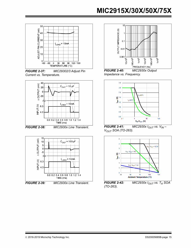
FIGURE 2-37: MIC29302/3 Adjust Pin Current vs. Temperature.
FIGURE 2-38: MIC2930x Line Transient.
FIGURE 2-39: MIC2930x Line Transient.
FIGURE 2-40: MIC2930x Output Impedance vs. Frequency.
FIGURE 2-41: MIC2930x IOUT vs. VIN – VOUT SOA (TO-263).
FIGURE 2-42: MIC2930x IOUT vs. TA SOA (TO-263).

MIC2915X/30X/50X/75X
DS20005685B-page 16 2016-2019 Microchip Technology Inc.
FIGURE 2-43: MIC2930x Short-Circuit SOA vs. Temperature (TO-263).
FIGURE 2-44: MIC2950x Dropout Voltage vs. Output Current.
FIGURE 2-45: MIC2950x Dropout Voltage vs. Temperature.
FIGURE 2-46: MIC29500-3.3 Dropout Characteristics.
FIGURE 2-47: MIC2950x Ground Current vs. Output Current.
FIGURE 2-48: MIC2950x Ground Current vs. Supply Voltage.
2016-2019 Microchip Technology Inc. DS20005685B-page 17
MIC2915X/30X/50X/75X
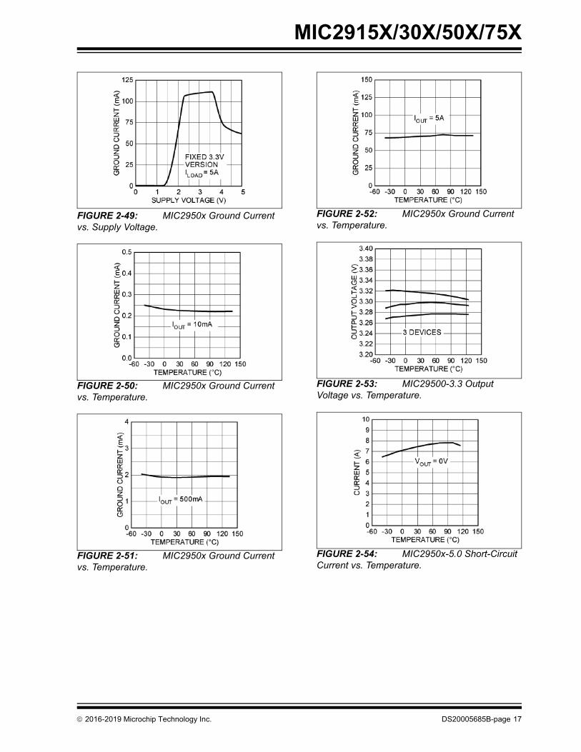
FIGURE 2-49: MIC2950x Ground Current vs. Supply Voltage.
FIGURE 2-50: MIC2950x Ground Current vs. Temperature.
FIGURE 2-51: MIC2950x Ground Current vs. Temperature.
FIGURE 2-52: MIC2950x Ground Current vs. Temperature.
FIGURE 2-53: MIC29500-3.3 Output Voltage vs. Temperature.
FIGURE 2-54: MIC2950x-5.0 Short-Circuit Current vs. Temperature.
MIC2915X/30X/50X/75X
DS20005685B-page 18 2016-2019 Microchip Technology Inc.
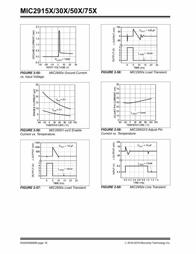
FIGURE 2-55: MIC2950x Ground Current vs. Input Voltage.
FIGURE 2-56: MIC29501-xx/2 Enable Current vs. Temperature.
FIGURE 2-57: MIC2950x Load Transient.
FIGURE 2-58: MIC2950x Load Transient.
FIGURE 2-59: MIC29502/3 Adjust Pin Current vs. Temperature.
FIGURE 2-60: MIC2950x Line Transient.

2016-2019 Microchip Technology Inc. DS20005685B-page 19
MIC2915X/30X/50X/75X
FIGURE 2-61: MIC2950x Line Transient.
FIGURE 2-62: MIC2950x Output Impedance vs. Frequency.
FIGURE 2-63: MIC2975x Dropout Voltage vs. Output Current.
FIGURE 2-64: MIC2975x Dropout Voltage vs. Temperature.
FIGURE 2-65: MIC29751-3.3 Dropout Characteristics.
FIGURE 2-66: MIC2975x Ground Current vs. Output Current.

MIC2915X/30X/50X/75X
DS20005685B-page 20 2016-2019 Microchip Technology Inc.
FIGURE 2-67: MIC2975x Ground Current vs. Supply Voltage.
FIGURE 2-68: MIC2975x Ground Current vs. Supply Voltage.
FIGURE 2-69: MIC2975x Ground Current vs. Temperature.
FIGURE 2-70: MIC2975x Ground Current vs. Temperature.
FIGURE 2-71: MIC2975x Ground Current vs. Temperature.
FIGURE 2-72: MIC29751-3.3 Output Voltage vs. Temperature.

2016-2019 Microchip Technology Inc. DS20005685B-page 21
MIC2915X/30X/50X/75X
FIGURE 2-73: MIC29751-5.0 Short-Circuit Current vs. Temperature.
FIGURE 2-74: MIC2975x Ground Current vs. Input Voltage.
FIGURE 2-75: MIC29751-xx/2 Enable Current vs. Temperature.
FIGURE 2-76: MIC2975x Load Transient.
FIGURE 2-77: MIC2975x Load Transient.
FIGURE 2-78: MIC29752 Adjust Pin Current vs. Temperature.

MIC2915X/30X/50X/75X
DS20005685B-page 22 2016-2019 Microchip Technology Inc.
FIGURE 2-79: MIC2975x Line Transient.
FIGURE 2-80: MIC2975x Line Transient.
FIGURE 2-81: MIC2975x Output Impedance vs. Frequency.
2016-2019 Microchip Technology Inc. DS20005685B-page 23
MIC2915X/30X/50X/75X
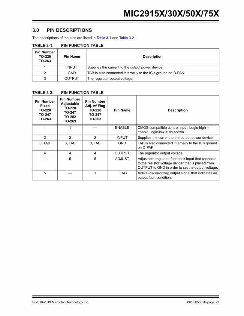
3.0 PIN DESCRIPTIONS
The descriptions of the pins are listed in Table 3-1 and Table 3-2.
TABLE 3-1: PIN FUNCTION TABLE
Pin NumberTO-220TO-263
Pin Name Description
1 INPUT Supplies the current to the output power device.
2 GND TAB is also connected internally to the IC’s ground on D-PAK.
3 OUTPUT The regulator output voltage.
TABLE 3-2: PIN FUNCTION TABLE
Pin NumberFixed
TO-220TO-247TO-263
Pin NumberAdjustable
TO-220TO-247TO-252TO-263
Pin NumberAdj. w/ Flag
TO-220TO-247TO-263
Pin Name Description
1 1 — ENABLE CMOS compatible control input. Logic-high = enable, logic-low = shutdown.
2 2 2 INPUT Supplies the current to the output power device.
3, TAB 3, TAB 3, TAB GND TAB is also connected internally to the IC’s ground on D-PAK.
4 4 4 OUTPUT The regulator output voltage.
— 5 5 ADJUST Adjustable regulator feedback input that connects to the resistor voltage divider that is placed from OUTPUT to GND in order to set the output voltage.
5 — 1 FLAG Active-low error flag output signal that indicates an output fault condition.

MIC2915X/30X/50X/75X
DS20005685B-page 24 2016-2019 Microchip Technology Inc.
4.0 APPLICATION INFORMATION
The MIC2915x, MIC2930x, MIC2950x, and MIC2975xare high-performance low-dropout voltage regulatorssuitable for all moderate to high-current voltageregulator applications. Their 350 mV to 425 mV typicaldropout voltage at full load make them especiallyvaluable in battery powered systems and as highefficiency noise filters in post-regulator applications.Unlike older NPN-pass transistor designs, where theminimum dropout voltage is limited by the base-emittervoltage drop and collector-emitter saturation voltage,dropout performance of the PNP output of thesedevices is limited merely by the low VCE saturationvoltage.
A trade-off for the low-dropout voltage is a varying basedriver requirement. But Microchip’s Super ßeta PNPprocess reduces this drive requirement to merely 1% ofthe load current.
The MIC2915x/2930x/2950x/2975x family of regulatorsare fully protected from damage due to fault conditions.Current limiting is provided. This limiting is linear;output current under overload conditions is constant.Thermal shutdown disables the device when the dietemperature exceeds the +125°C maximum safeoperating temperature. Line transient protection allowsdevice and load survival even when the input voltagespikes between –20V and +60V. When the inputvoltage exceeds approximately 32V, the overvoltagesensor disables the regulator. The output structure ofthese regulators allows voltages in excess of thedesired output voltage to be applied without reversecurrent flow. MIC29xx1 and MIC29xx2 versions offer alogic-level ON/OFF control. When disabled, thedevices draw nearly zero current.
An additional feature of this regulator family is acommon pinout. A design’s current requirement maychange up or down, but use the same board layoutbecause all of these regulators have identical pinouts.
FIGURE 4-1: Linear Regulators Require Only Two Capacitors for Operation.
4.1 Thermal Design
Linear regulators are simple to use. The mostcomplicated design parameters to consider are thermalcharacteristics. Thermal design requires the followingapplication-specific parameters:
• Maximum Ambient Temperature, TA
• Output Current, IOUT
• Output Voltage, VOUT
• Input Voltage, VIN
First, calculate the power dissipation of the regulatorfrom these numbers and the device parameters fromthis data sheet.
EQUATION 4-1:
The ground current is approximated by 1% of IOUT.Then the heat sink thermal resistance is determinedwith Equation 4-2.
EQUATION 4-2:
The heat sink may be significantly reduced inapplications where the minimum input voltage is knownand is large compared with the dropout voltage. Use aseries input resistor to drop excessive voltage anddistribute the heat between this resistor and theregulator. The low-dropout properties of Super ßetaPNP regulators allow very significant reductions inregulator power dissipation and the associated heatsink without compromising performance. When thistechnique is employed, a capacitor of at least 0.1 µF isneeded directly between the input and regulatorground.
Please refer to Application Note 9 and Application Hint17 for further details and examples on thermal designand heat sink specification.
With no heat sink in the application, calculate thejunction temperature to determine the maximum powerdissipation that will be allowed before exceeding themaximum junction temperature of the MIC29152. Themaximum power allowed can be calculated using the
MIC29xxx
VIN IN VOUTOUT
GND
PD IOUT 1.01 VIN VOUT– =
SATJMAX TA–
PD---------------------------- JC CS+ –=
Where:
TJMAX ≤ 125°C
θCS Between 0°C/W and 2°C/W
2016-2019 Microchip Technology Inc. DS20005685B-page 25
MIC2915X/30X/50X/75X
thermal resistance (θJA) of the D-Pak adhering to thefollowing criteria for the PCB design: 2 oz. copper and100 mm2 copper area for the MIC29152.
For example, given an expected maximum ambienttemperature (TA) of +75°C with VIN = 3.3V, VOUT =2.5V, and IOUT = 1.5A, first calculate the expected PDusing Equation 4-3:
EQUATION 4-3:
Next, calculate the junction temperature for theexpected power dissipation.
EQUATION 4-4:
Now determine the maximum power dissipationallowed that would not exceed the IC’s maximumjunction temperature (+125°C) without the use of aheat sink.
EQUATION 4-5:
4.2 Capacitor Requirements
For stability and minimum output noise, a capacitor onthe regulator output is necessary. The value of thiscapacitor is dependent upon the output current; lowercurrents allow smaller capacitors. TheMIC2915x/2930x/2950x/2975x regulators are stablewith the following minimum capacitor values at full load,as noted in Table 4-1.
This capacitor need not be an expensive low ESR type:aluminum electrolytics are adequate. In fact, extremelylow ESR capacitors may contribute to instability.Tantalum capacitors are recommended for systemswhere fast load transient response is important.
Where the regulator is powered from a source with highAC impedance, a 0.1 µF capacitor connected betweenInput and GND is recommended. This capacitor shouldhave good characteristics to above 250 kHz.
4.3 Minimum Load Current
The MIC2915x–2975x regulators are specifiedbetween finite loads. If the output current is too small,leakage currents dominate and the output voltagerises. The following minimum load current swamps anyexpected leakage current across the operatingtemperature range, as shown in Table 4-2.
4.4 Adjustable Regulator Design
The adjustable regulator versions, MIC29xx2 andMIC29xx3, allow programming the output voltageanywhere between 1.25V and the 25V. Two resistorsare used. The resistor values are calculated byEquation 4-6.
EQUATION 4-6:
In the equation above, VOUT is the desired outputvoltage. Figure 4-2 shows component definition.Applications with widely varying load currents mayscale the resistors to draw the minimum load currentrequired for proper operation (see the Minimum LoadCurrent sub-section).TABLE 4-1: MINIMUM CAPACITOR
VALUES AT FULL LOAD
Device Full-Load Capacitor
MIC2915x 10 µF
MIC2930x 10 µF
MIC2950x 10 µF
MIC2975x 22 µF
PD 3.3V 2.5V– 1.5A 3.3V 0.016A 1.1472W=–=
TJ JA PD TA+
56oC/W 1.1472W 75
oC+ 139.24
oC
=
= =
PD MAX TJ MAX TA– JA
125oC 75
oC– 56
oC/W 0.893W
=
= =
TABLE 4-2: MINIMUM LOAD CURRENTS
Device Minimum Load
MIC2915x 5 mA
MIC2930x 7 mA
MIC2950x 10 mA
MIC2975x 10 mA
R1 R2VOUT1.240------------- 1– =

MIC2915X/30X/50X/75X
DS20005685B-page 26 2016-2019 Microchip Technology Inc.
FIGURE 4-2: Adjustable Regulator with Resistors.
4.5 Error Flag
MIC29xx1 and MIC29xx3 versions feature an ErrorFlag, which looks at the output voltage and signals anerror condition when this voltage drops 5% below itsexpected value. The error flag is an open-collectoroutput that pulls low under fault conditions. It may sink10 mA. Low output voltage signifies a number ofpossible problems, including an overcurrent fault (thedevice is in current-limit) and low input voltage. The flagoutput is inoperative during overtemperature shutdownconditions.
4.6 Enable Input
MIC29xx1 and MIC29xx2 versions feature an enable(EN) input that allows ON/OFF control of the device.Special design allows “zero” current drain when thedevice is disabled; only microamperes of leakagecurrent flows. The EN input has TTL/CMOS compatiblethresholds for simple interfacing with logic, or may bedirectly tied to ≤30V. Enabling the regulator requiresapproximately 20 µA of current.
R1
R2
VIN VOUT
MIC29152
22μF10μF

2016-2019 Microchip Technology Inc. DS20005685B-page 27
MIC2915X/30X/50X/75X
5.0 PACKAGING INFORMATION
5.1 Package Marking Information
3- and 5-Pin TO-263 (Fixed)* Example
XXXXXXXX
WNNNPX.XXX
5-Pin TO-263 (Adjustable)* Example
MIC29150
8943P3.3WU
XXXXXXXXXXWNNNP
MIC29152WU6235P
3- and 5-Pin TO-220 (Fixed)* Example
XXXXX
WNNNPX.XXX
5-Pin TO-220 (Adjustable)* Example
XXXXXXXXXXWNNNP
MIC29302WT7404P
29301
1586P5.0WT

MIC2915X/30X/50X/75X
DS20005685B-page 28 2016-2019 Microchip Technology Inc.
5-Pin TO-252* Example
XXXXXXXXXXWNNNP<BS1><COO>
MIC29152WD3102P USA
5-Pin TO-247 (Fixed)* Example
XXXXX
WNNNPXXXXXXXX-X.XXXX
5-Pin TO-247 (Adjustable)* Example
<COO>YYWWNNN
MICREL
5943PMIC29751-3.3WWT
USA1642815
XXXXX
WNNNPXXXXXXXXXXX
<COO>YYWWNNN
MICREL
2359PMIC29752WWT
USA1521108
Legend: XX...X Product code or customer-specific informationY Year code (last digit of calendar year)YY Year code (last 2 digits of calendar year)WW Week code (week of January 1 is week ‘01’)NNN Alphanumeric traceability code Pb-free JEDEC® designator for Matte Tin (Sn)* This package is Pb-free. The Pb-free JEDEC designator ( )
can be found on the outer packaging for this package.
●, ▲, ▼ Pin one index is identified by a dot, delta up, or delta down (trianglemark).
Note: In the event the full Microchip part number cannot be marked on one line, it willbe carried over to the next line, thus limiting the number of availablecharacters for customer-specific information. Package may or may not includethe corporate logo.
Underbar (_) and/or Overbar (⎯) symbol may not be to scale.
3e
3e

2016-2019 Microchip Technology Inc. DS20005685B-page 29
MIC2915X/30X/50X/75X
3-Lead TO-220 Package Outline and Recommended Land Pattern
Note: For the most current package drawings, please see the Microchip Packaging Specification located at http://www.microchip.com/packaging.

MIC2915X/30X/50X/75X
DS20005685B-page 30 2016-2019 Microchip Technology Inc.
5-Lead TO-220 Package Outline and Recommended Land Pattern
Note: For the most current package drawings, please see the Microchip Packaging Specification located at http://www.microchip.com/packaging.

2016-2019 Microchip Technology Inc. DS20005685B-page 31
MIC2915X/30X/50X/75X
5-Lead TO-263 (DDPAK) Package Outline and Recommended Land Pattern
���������� �������������
�������� ������������ �!����� ��" ����� ��# �"���"�����$�%�$���� �����&$ �#��$����"������� �&"���"�����$����"������� �&"���"�"������� � '� $����()� ��"�$ �*� ��# �"���������$� �� �������� �����%�+���(��
,�!- ,�"�����# �"������� �� ������� '�� �.��& �"��/��/� ��& � �� ���� "�
����� 0��� � �#�" ��&�� � ���1�� �$��/���"2�� �" �" � � ����������3��1������� ������ �������� $�� �� -44///�#����������#4��1�����
5�� " �6!7%���# �"����8�#� " ��6 69� ��:
6&#; �����3��" 6 (3� �� ��<��,�!9. �����7 ��� � ��<� = ����� ��$������ �� ���� = ����9. �����>�$ � % �*?� = ����%'�" $�3�$�>�$ � %� ���( = =���$ $�3��1�� �8 �� � � �**� = �*?�9. �����8 �� � 7 �(�� = �<�(%'�" $�3�$�8 �� � �� ���� = =8 �$�����1� "" � ���� = ����3�$�����1� "" !� ���( = ��<(8 �$�>�$ � ; ���� = ��*�0�� �8 �� � 8 ��<? = ����3�$�8 �� � 8� = = ��<�0�� ����� � �@ = ?@
E
L1
D
D1
H
N1
b e
TOP VIEW
BOTTOM VIEW
A
A1 c L
C2
CHAMFEROPTIONAL
E1
φ
�������� � �������� ���/��� !�����,

MIC2915X/30X/50X/75X
DS20005685B-page 32 2016-2019 Microchip Technology Inc.
Note: For the most current package drawings, please see the Microchip Packaging Specification located at http://www.microchip.com/packaging

2016-2019 Microchip Technology Inc. DS20005685B-page 33
MIC2915X/30X/50X/75X
3-Lead TO-263 Package Outline and Recommended Land Pattern
Note: For the most current package drawings, please see the Microchip Packaging Specification located at http://www.microchip.com/packaging.

MIC2915X/30X/50X/75X
DS20005685B-page 34 2016-2019 Microchip Technology Inc.
5-Lead TO-247 Package Outline and Recommended Land Pattern
Note: For the most current package drawings, please see the Microchip Packaging Specification located at http://www.microchip.com/packaging.

2016-2019 Microchip Technology Inc. DS20005685B-page 35
MIC2915X/30X/50X/75X
5-Lead TO-252 Package Outline and Recommended Land Pattern
Note: For the most current package drawings, please see the Microchip Packaging Specification located at http://www.microchip.com/packaging.

MIC2915X/30X/50X/75X
DS20005685B-page 36 2016-2019 Microchip Technology Inc.
NOTES:
2016-2019 Microchip Technology Inc. DS20005685B-page 37
MIC2915X/30X/50X/75X
APPENDIX A: REVISION HISTORY
Revision A (December 2016)
• Converted Micrel document MIC2915x/30x/50x/75x to Microchip data sheet DS20005685A.
• Minor text changes throughout.
• Removed references to the discontinued MIC29750.
• Added Figure 2-41, Figure 2-42, and Figure 2-43.
• Removed the 3-Pin TO-247 package option.
Revision B (January 2019)
• Updated package drawing for 5-Lead TO-263 (DDPAK) Package Outline and Recommended Land Pattern option.

MIC2915X/30X/50X/75X
DS20005685B-page 38 2016-2019 Microchip Technology Inc.
NOTES:

2016-2019 Microchip Technology Inc. DS20005685B-page 39
MIC2915X/30X/50X/75X
PRODUCT IDENTIFICATION SYSTEM
To order or obtain information, e.g., on pricing or delivery, contact your local Microchip representative or sales office.
Examples:
a) MIC29150-3.3WT: 1.5A High-Current Low-Dropout Regulator, 3.3V, –40°C to +125°C TemperatureRange, 3-Lead TO-220, 50/Tube
b) MIC29152WD-TR: 1.5A High-Current Low-Dropout Regulator, Adjustable Voltage,
–40°C to +125°C TemperatureRange, 5-Lead TO-252, 2,500/Reel
c) MIC29302WU: 3A High-Current Low-Dropout Regulator,Adjustable Voltage, –40°C to +125°C TemperatureRange, 5-Lead TO-263, 50/Tube
d) MIC29301-12WU-TR: 3A High-Current Low-Dropout Regulator, 12V, –40°C to +125°C TemperatureRange, 5-Lead TO-263, 750/Reel
e) MIC29500-5.0WT: 5A High-Current Low-Dropout Regulator, 5.0V, –40°C to +125°C TemperatureRange, 3-Lead TO-220, 50/Tube
f) MIC29503WT: 5A High-Current Low-Dropout Regulator,Adjustable Voltage, –40°C to +125°C TemperatureRange, 5-Lead TO-220, 50/Tube
g) MIC29751-3.3WWT-TR:7.5A High-Current Low-Dropout Regulator, 3.3V, –40°C to +125°C TemperatureRange, 5-Lead TO-247, 2,500/Reel
h) MIC29752WWT: 7.5A High-Current Low-Dropout Regulator,Adjustable Voltage, –40°C to +125°C TemperatureRange, 5-Lead TO-247, 30/Tube
PART NO. X
JunctionDevice
Device: MIC2915x: 1.5A High-Current Low-Dropout RegulatorMIC2930x: 3A High-Current Low-Dropout RegulatorMIC2950x: 5A High-Current Low-Dropout RegulatorMIC2975x: 7.5A High-Current Low-Dropout Regulator
Voltage: 3.3 = 3.3V5.0 = 5.0V12 = 12V(blank) = Adjustable
JunctionTemperature Range:
W = –40°C to +125°C
Package: U = 3-Lead or 5-Lead TO-263T = 3-Lead or 5-Lead TO-220D = 5-Lead TO-252WT = 5-Lead TO-247
Media Type: TR = 2,500/Reel for D and WT PackagesTR = 750/Reel for U Package(blank)= 50/Tube for U, T, and D Packages(blank)= 30/Tube for WT Package
XX
Voltage
XX –
Media Type
Note 1: Tape and Reel identifier only appears in the catalog part number description. This identifier is used for ordering purposes and is not printed on the device package. Check with your Microchip Sales Office for package availability with the Tape and Reel option.
–
Temperature Range
X
Package

MIC2915X/30X/50X/75X
DS20005685B-page 40 2016-2019 Microchip Technology Inc.
NOTES:

2016-2019 Microchip Technology Inc. DS20005685B-page 41
Information contained in this publication regarding deviceapplications and the like is provided only for your convenienceand may be superseded by updates. It is your responsibility toensure that your application meets with your specifications.MICROCHIP MAKES NO REPRESENTATIONS ORWARRANTIES OF ANY KIND WHETHER EXPRESS ORIMPLIED, WRITTEN OR ORAL, STATUTORY OROTHERWISE, RELATED TO THE INFORMATION,INCLUDING BUT NOT LIMITED TO ITS CONDITION,QUALITY, PERFORMANCE, MERCHANTABILITY ORFITNESS FOR PURPOSE. Microchip disclaims all liabilityarising from this information and its use. Use of Microchipdevices in life support and/or safety applications is entirely atthe buyer’s risk, and the buyer agrees to defend, indemnify andhold harmless Microchip from any and all damages, claims,suits, or expenses resulting from such use. No licenses areconveyed, implicitly or otherwise, under any Microchipintellectual property rights unless otherwise stated.
Trademarks
The Microchip name and logo, the Microchip logo, AnyRate, AVR, AVR logo, AVR Freaks, BitCloud, chipKIT, chipKIT logo, CryptoMemory, CryptoRF, dsPIC, FlashFlex, flexPWR, Heldo, JukeBlox, KeeLoq, Kleer, LANCheck, LINK MD, maXStylus, maXTouch, MediaLB, megaAVR, MOST, MOST logo, MPLAB, OptoLyzer, PIC, picoPower, PICSTART, PIC32 logo, Prochip Designer, QTouch, SAM-BA, SpyNIC, SST, SST Logo, SuperFlash, tinyAVR, UNI/O, and XMEGA are registered trademarks of Microchip Technology Incorporated in the U.S.A. and other countries.
ClockWorks, The Embedded Control Solutions Company, EtherSynch, Hyper Speed Control, HyperLight Load, IntelliMOS, mTouch, Precision Edge, and Quiet-Wire are registered trademarks of Microchip Technology Incorporated in the U.S.A.
Adjacent Key Suppression, AKS, Analog-for-the-Digital Age, Any Capacitor, AnyIn, AnyOut, BodyCom, CodeGuard, CryptoAuthentication, CryptoAutomotive, CryptoCompanion, CryptoController, dsPICDEM, dsPICDEM.net, Dynamic Average Matching, DAM, ECAN, EtherGREEN, In-Circuit Serial Programming, ICSP, INICnet, Inter-Chip Connectivity, JitterBlocker, KleerNet, KleerNet logo, memBrain, Mindi, MiWi, motorBench, MPASM, MPF, MPLAB Certified logo, MPLIB, MPLINK, MultiTRAK, NetDetach, Omniscient Code Generation, PICDEM, PICDEM.net, PICkit, PICtail, PowerSmart, PureSilicon, QMatrix, REAL ICE, Ripple Blocker, SAM-ICE, Serial Quad I/O, SMART-I.S., SQI, SuperSwitcher, SuperSwitcher II, Total Endurance, TSHARC, USBCheck, VariSense, ViewSpan, WiperLock, Wireless DNA, and ZENA are trademarks of Microchip Technology Incorporated in the U.S.A. and other countries.
SQTP is a service mark of Microchip Technology Incorporated in the U.S.A.
Silicon Storage Technology is a registered trademark of Microchip Technology Inc. in other countries.
GestIC is a registered trademark of Microchip Technology Germany II GmbH & Co. KG, a subsidiary of Microchip Technology Inc., in other countries.
All other trademarks mentioned herein are property of their respective companies.
© 2016-2019, Microchip Technology Incorporated, All Rights Reserved.
ISBN: 978-1-5224-4105-2
Note the following details of the code protection feature on Microchip devices:
• Microchip products meet the specification contained in their particular Microchip Data Sheet.
• Microchip believes that its family of products is one of the most secure families of its kind on the market today, when used in the intended manner and under normal conditions.
• There are dishonest and possibly illegal methods used to breach the code protection feature. All of these methods, to our knowledge, require using the Microchip products in a manner outside the operating specifications contained in Microchip’s Data Sheets. Most likely, the person doing so is engaged in theft of intellectual property.
• Microchip is willing to work with the customer who is concerned about the integrity of their code.
• Neither Microchip nor any other semiconductor manufacturer can guarantee the security of their code. Code protection does not mean that we are guaranteeing the product as “unbreakable.”
Code protection is constantly evolving. We at Microchip are committed to continuously improving the code protection features of ourproducts. Attempts to break Microchip’s code protection feature may be a violation of the Digital Millennium Copyright Act. If such actsallow unauthorized access to your software or other copyrighted work, you may have a right to sue for relief under that Act.
Microchip received ISO/TS-16949:2009 certification for its worldwide headquarters, design and wafer fabrication facilities in Chandler and Tempe, Arizona; Gresham, Oregon and design centers in California and India. The Company’s quality system processes and procedures are for its PIC® MCUs and dsPIC® DSCs, KEELOQ® code hopping devices, Serial EEPROMs, microperipherals, nonvolatile memory and analog products. In addition, Microchip’s quality system for the design and manufacture of development systems is ISO 9001:2000 certified.
QUALITYMANAGEMENTSYSTEMCERTIFIEDBYDNV
== ISO/TS16949==

DS20005685B-page 42 2016-2019 Microchip Technology Inc.
AMERICASCorporate Office2355 West Chandler Blvd.Chandler, AZ 85224-6199Tel: 480-792-7200 Fax: 480-792-7277Technical Support: http://www.microchip.com/supportWeb Address: www.microchip.com
AtlantaDuluth, GA Tel: 678-957-9614 Fax: 678-957-1455
Austin, TXTel: 512-257-3370
BostonWestborough, MA Tel: 774-760-0087 Fax: 774-760-0088
ChicagoItasca, IL Tel: 630-285-0071 Fax: 630-285-0075
DallasAddison, TX Tel: 972-818-7423 Fax: 972-818-2924
DetroitNovi, MI Tel: 248-848-4000
Houston, TX Tel: 281-894-5983
IndianapolisNoblesville, IN Tel: 317-773-8323Fax: 317-773-5453Tel: 317-536-2380
Los AngelesMission Viejo, CA Tel: 949-462-9523Fax: 949-462-9608Tel: 951-273-7800
Raleigh, NC Tel: 919-844-7510
New York, NY Tel: 631-435-6000
San Jose, CA Tel: 408-735-9110Tel: 408-436-4270
Canada - TorontoTel: 905-695-1980 Fax: 905-695-2078
ASIA/PACIFICAustralia - SydneyTel: 61-2-9868-6733
China - BeijingTel: 86-10-8569-7000
China - ChengduTel: 86-28-8665-5511
China - ChongqingTel: 86-23-8980-9588
China - DongguanTel: 86-769-8702-9880
China - GuangzhouTel: 86-20-8755-8029
China - HangzhouTel: 86-571-8792-8115
China - Hong Kong SARTel: 852-2943-5100
China - NanjingTel: 86-25-8473-2460
China - QingdaoTel: 86-532-8502-7355
China - ShanghaiTel: 86-21-3326-8000
China - ShenyangTel: 86-24-2334-2829
China - ShenzhenTel: 86-755-8864-2200
China - SuzhouTel: 86-186-6233-1526
China - WuhanTel: 86-27-5980-5300
China - XianTel: 86-29-8833-7252
China - XiamenTel: 86-592-2388138
China - ZhuhaiTel: 86-756-3210040
ASIA/PACIFICIndia - BangaloreTel: 91-80-3090-4444
India - New DelhiTel: 91-11-4160-8631
India - PuneTel: 91-20-4121-0141
Japan - OsakaTel: 81-6-6152-7160
Japan - TokyoTel: 81-3-6880- 3770
Korea - DaeguTel: 82-53-744-4301
Korea - SeoulTel: 82-2-554-7200
Malaysia - Kuala LumpurTel: 60-3-7651-7906
Malaysia - PenangTel: 60-4-227-8870
Philippines - ManilaTel: 63-2-634-9065
SingaporeTel: 65-6334-8870
Taiwan - Hsin ChuTel: 886-3-577-8366
Taiwan - KaohsiungTel: 886-7-213-7830
Taiwan - TaipeiTel: 886-2-2508-8600
Thailand - BangkokTel: 66-2-694-1351
Vietnam - Ho Chi MinhTel: 84-28-5448-2100
EUROPEAustria - WelsTel: 43-7242-2244-39Fax: 43-7242-2244-393
Denmark - CopenhagenTel: 45-4450-2828 Fax: 45-4485-2829
Finland - EspooTel: 358-9-4520-820
France - ParisTel: 33-1-69-53-63-20 Fax: 33-1-69-30-90-79
Germany - GarchingTel: 49-8931-9700
Germany - HaanTel: 49-2129-3766400
Germany - HeilbronnTel: 49-7131-67-3636
Germany - KarlsruheTel: 49-721-625370
Germany - MunichTel: 49-89-627-144-0 Fax: 49-89-627-144-44
Germany - RosenheimTel: 49-8031-354-560
Israel - Ra’anana Tel: 972-9-744-7705
Italy - Milan Tel: 39-0331-742611 Fax: 39-0331-466781
Italy - PadovaTel: 39-049-7625286
Netherlands - DrunenTel: 31-416-690399 Fax: 31-416-690340
Norway - TrondheimTel: 47-7288-4388
Poland - WarsawTel: 48-22-3325737
Romania - BucharestTel: 40-21-407-87-50
Spain - MadridTel: 34-91-708-08-90Fax: 34-91-708-08-91
Sweden - GothenbergTel: 46-31-704-60-40
Sweden - StockholmTel: 46-8-5090-4654
UK - WokinghamTel: 44-118-921-5800Fax: 44-118-921-5820
Worldwide Sales and Service
08/15/18