references and low dropout linear regulators - analog devices
TRANSCRIPT

REFERENCES AND LOW DROPOUT LINEAR REGULATORS
2.1
SECTION 2
REFERENCES AND LOW DROPOUT LINEARREGULATORS
Walt Jung
Reference circuits and linear regulators actually have much in common. In fact, thelatter could be functionally described as a reference circuit, but with greater current(or power) output. Accordingly, almost all of the specifications of the two circuittypes have great commonality (even though the performance of references is usuallytighter with regard to drift, accuracy, etc.). This chapter is broadly divided into aninitial discussion on voltage references, followed by a concluding discussion on linearregulators, with emphasis on their low dropout operation for highest powerefficiency.
PRECISION VOLTAGE REFERENCES
Walt Jung, Walt Kester, James Bryant
Voltage references have a major impact on the performance and accuracy of analogsystems. A ±5mV tolerance on a 5V reference corresponds to ±0.1% absoluteaccuracy–only 10-bits. For a 12-bit system, choosing a reference that has a ±1mVtolerance may be far more cost effective than performing manual calibration, whileboth high initial accuracy and calibration will be necessary in a system makingabsolute 16-bit measurements. Note that many systems make relativemeasurements rather than absolute ones, and in such cases the absolute accuracy ofthe reference is not important, although noise and short-term stability may be.Figure 2.1 summarizes some key points of the reference selection process.
Temperature drift or drift due to aging may be an even greater problem thanabsolute accuracy. The initial error can always be trimmed, but compensating fordrift is difficult. Where possible, references should be chosen for temperaturecoefficient and aging characteristics which preserve adequate accuracy over theoperating temperature range and expected lifetime of the system.
Noise in voltage references is often overlooked, but it can be very important insystem design. It is generally specified on data sheets, but system designersfrequently ignore the specification and assume that voltage references do notcontribute to system noise.
There are two dynamic issues that must be considered with voltage references: theirbehavior at start-up, and their behavior with transient loads. With regard to thefirst, always bear in mind that voltage references do not power up instantly (this istrue of references inside ADCs and DACs as well as discrete designs). Thus it israrely possible to turn on an ADC and reference, whether internal or external, make

REFERENCES AND LOW DROPOUT LINEAR REGULATORS
2.2
a reading, and turn off again within a few microseconds, however attractive such aprocedure might be in terms of energy saving.
Regarding the second point, a given reference IC may or may not be well suited forpulse-loading conditions, dependent upon the specific architecture. Many referencesuse low power, and therefore low bandwidth, output buffer amplifiers. This makesfor poor behavior under fast transient loads, which may degrade the performance offast ADCs (especially successive approximation and flash ADCs). Suitabledecoupling can ease the problem (but some references oscillate with capacitiveloads), or an additional external broadband buffer amplifier may be used to drive thenode where the transients occur.
References, like almost all other ICs today, are fast migrating to such smallerpackages such as SO-8, and the even more tiny SOT-23, enabling much highercircuit densities within a given area of real estate. In addition to the system sizereductions these steps bring, there are also tangible reductions in standby powerand cost with the smaller and less expense ICs.
CHOOSING VOLTAGE REFERENCESFOR HIGH PERFORMANCE SYSTEMS
n Tight Tolerance Improves Accuracy, Reduces System Costs
n Temperature Drift Affects Accuracy
n Long-Term Stability, Low Hysteresis Assures Repeatability
n Noise Limits System Resolution
n Dynamic Loading Can Cause Errors
n Power Consumption is Critical to Battery Systems
n Tiny Low Cost Packages Increase Circuit Density
Figure 2.1
TYPES OF VOLTAGE REFERENCES
In terms of the functionality of their circuit connection, standard reference ICs areoften only available in series, or three-terminal form (VIN, Common, VOUT), andalso in positive polarity only. The series types have the potential advantages oflower and more stable quiescent current, standard pre-trimmed output voltages, andrelatively high output current without accuracy loss. Shunt, or two-terminal (i.e.,diode-like) references are more flexible regarding operating polarity, but they arealso more restrictive as to loading. They can in fact eat up excessive power withwidely varying resistor-fed voltage inputs. Also, they sometimes come in non-standard voltages. All of these various factors tend to govern when one functionaltype is preferred over the other.

REFERENCES AND LOW DROPOUT LINEAR REGULATORS
2.3
Some simple diode-based references are shown in Figure 2.2. In the first of these, acurrent driven forward biased diode (or diode-connected transistor) produces avoltage, Vf = VREF. While the junction drop is somewhat decoupled from the rawsupply, it has numerous deficiencies as a reference. Among them are a strong TC ofabout –0.3%/°C, some sensitivity to loading, and a rather inflexible output voltage: itis only available in 600mV jumps.
By contrast, these most simple references (as well as all other shunt-type regulators)have a basic advantage, which is the fact that the polarity is readily reversible byflipping connections and reversing the drive current. However, a basic limitation ofall shunt regulators is that load current must always be less (usually appreciablyless) than the driving current, ID.
SIMPLE DIODE REFERENCE CIRCUITS
RS RZ
+VS +VS
D1
D1
D2
VREF VREF
ID IZ
FORWARD-BIASEDDIODE
ZENER (AVALANCHE)DIODE
Figure 2.2
In the second circuit of Figure 2.2, a zener or avalanche diode is used, and anappreciably higher output voltage realized. While true zener breakdown occursbelow 5V, avalanche breakdown occurs at higher voltages and has a positivetemperature coefficient. Note that diode reverse breakdown is referred to almostuniversally today as zener, even though it is usually avalanche breakdown. With aD1 breakdown voltage in the 5 to 8V range, the net positive TC is such that itequals the negative TC of forward-biased diode D2, yielding a net TC of 100ppm/°Cor less with proper bias current. Combinations of such carefully chosen diodesformed the basis of the early single package "temperature-compensated zener"references, such as the 1N821-1N829 series.
The temperature-compensated zener reference is limited in terms of initial accuracy,since the best TC combinations fall at odd voltages, such as the 1N829's 6.2V. And,

REFERENCES AND LOW DROPOUT LINEAR REGULATORS
2.4
the scheme is also limited for loading, since for best TC the diode current must becarefully controlled. Unlike a fundamentally lower voltage (<2V) reference, zenerdiode based references must of necessity be driven from voltage sources appreciablyhigher than 6V levels, so this precludes operation of zener references from 5Vsystem supplies. References based on low TC zener (avalanche) diodes also tend tobe noisy, due to the basic noise of the breakdown mechanism. This has beenimproved greatly with monolithic zener types, as is described further below.
At this point, we know that a reference circuit can be functionally arranged intoeither a series or shunt operated form, and the technology within may use eitherbandgap based or zener diode based circuitry. In practice there are all permutationsof these available, as well as a third major technology category. The three majorreference technologies are now described in more detail.
BANDGAP REFERENCES
The development of low voltage (<5V) references based on the bandgap voltage ofsilicon led to the introductions of various ICs which could be operated on low voltagesupplies with good TC performance. The first of these was the LM109 (Reference 1),and a basic bandgap reference cell is shown in Figure 2.3.
BASIC BANDGAP REFERENCE
R1600ΩΩ
R26kΩΩ
Q1
Q2
Q3
R3600ΩΩ
VR = VBE +
∆∆VBE VBE
∆∆VBER2R3
+VS
IZ
∆∆VBER2R3
Figure 2.3

REFERENCES AND LOW DROPOUT LINEAR REGULATORS
2.5
This circuit is also called a "∆VBE" reference because the differing current densitiesbetween matched transistors Q1-Q2 produces a ∆VBE across R3. It works bysumming the VBE of Q3 with the amplified ∆VBE of Q1-Q2, developed across R2.The ∆VBE and VBE components have opposite polarity TCs; ∆VBE is proportional-to-absolute-temperature (PTAT), while VBE is complementary-to-absolute-temperature (CTAT). The summed output is VR, and when it is equal to 1.205V(silicon bandgap voltage), the TC is a minimum.
The bandgap reference technique is attractive in IC designs because of severalreasons; among these are the relative simplicity, and the avoidance of zeners andtheir noise. However, very important in these days of ever decreasing systemsupplies is the fundamental fact that bandgap devices operate at low voltages, i.e.,<5V. Not only are they used for stand-alone IC references, but they are also usedwithin the designs of many other linear ICs such as ADCs, DACs, and op-amps.
Buffered forms of 1.2V two terminal bandgap references, such as the AD589 IC,remain stable under varying load currents. The H-02A metal can AD589, a 1.235Vreference, handles 50µA to 5mA with an output impedance of 0.6Ω, and TCs rangingbetween 10 and 100ppm/°C. The more recent and functionally similar AD1580, a1.225V reference, is in the tiny SOT-23 package and handles the same nominalcurrents as the AD589, with TCs of 50 and 100ppm/°C.
However, the basic designs of Figure 2.3 suffer from load and current drivesensitivity, plus the fact that the output needs accurate scaling to more useful levels,i.e., 2.5V, 5V, etc. The load drive issue is best addressed with the use of a bufferamplifier, which also provides convenient voltage scaling to standard levels.
An improved three-terminal bandgap reference, the AD580, is shown in Figure 2.4.Popularly called the "Brokaw Cell" (see References 2 and 3), this circuit provides on-chip output buffering, which allows good drive capability and standard outputvoltage scaling. The AD580 was the first precision bandgap based IC reference, andvariants of the topology have influenced further generations of both industrystandard references such as the REF01 and REF02 series, as well as more recentADI parts such as the REF195 series, the AD680, AD780, and the AD1582-85series.
The AD580 has two 8:1 emitter-scaled transistors Q1-Q2 operating at identicalcollector currents (and thus 1/8 current densities), by virtue of equal load resistorsand a closed loop around the buffer op-amp. Due to the resultant smaller VBE of the8× area Q2, R2 in series with Q2 drops the ∆VBE voltage, while R1 (due to thecurrent relationships) drops a PTAT voltage V1:
V1 2R1R2
VBE= × × ∆ .

REFERENCES AND LOW DROPOUT LINEAR REGULATORS
2.6
AD580 PRECISION BANDGAPREFERENCE USES BROKAW CELL
R8 R7
+I2 ≅ ≅ I1
Q28A
Q1
A
R2
R1 ∆∆VBER1R2
R4
R5∆∆VBE
VBE(Q1)
V1 = 2
VZ = 1.205V
VOUT = 2.5V
+VIN
COM
A = TRANSISTOR AREA
Figure 2.4
The bandgap cell reference voltage VZ appears at the base of Q1, and is the sum ofVBE(Q1) and V1, or 1.205V, the bandgap voltage:
VZ VBE(Q1) V1= +
= + × ×VBE(Q1) 2R1R2
VBE∆
= + × × ×VBE(Q1) 2R1R2
kTq
lnJ1J2
= + × × ×VBE(Q1) 2R1R2
kTq
ln8
= 1.205V .
Note that J1 = current density in Q1, J2 = current density in Q2, and J1/J2 = 8.
However, because of the presence of the R4/R5 (laser trimmed) thin film divider andthe op-amp, the actual voltage appearing at VOUT can be scaled higher, in theAD580 case 2.5V. Following this general principle, VOUT can be raised to otherpractical levels, such as for example in the AD584, with taps for precise 2.5, 5, 7.5,and 10V operation. The AD580 provides up to 10mA output current while operatingfrom supplies between 4.5 and 30V. It is available in tolerances as low as 10mV,with TCs as low as 10ppm/°C.

REFERENCES AND LOW DROPOUT LINEAR REGULATORS
2.7
Many of the recent developments in bandgap references have focused on smallerpackage size and cost reduction, to address system needs for smaller, more powerefficient and less costly reference ICs. Among these are several recent bandgapbased IC references.
The AD1580 is a shunt mode IC reference which is functionally quite similar to theclassic shunt IC reference, the AD589 mentioned above. A key difference is the factthat the AD1580 uses a newer, small geometry process, enabling its availabilitywithin the tiny SOT-23 package. The very small size of this package allows use in awide variety of space limited applications, and the low operating current lends itselfto portable battery powered uses. The AD1580 circuit is shown in simplified form inFigure 2.5.
AD1580 1.2V SHUNT TYPE BANDGAP REFERENCE HAS TINY SIZE IN SOT-23 FOOTPRINT
R1
R2
R3
R4
VBE
+
–
∆∆VBE
+
–
V1
+
–
R5
R7
Q3 Q4
Q5
Q8
Q9
Q1
Q2
V+
V–
R6
Figure 2.5
In this circuit, like transistors Q1 and Q2 form the bandgap core, and are operatedat a current ratio of 5 times, determined by the ratio of R7 to R2. An op amp isformed by the differential pair Q3-Q4, current mirror Q5, and driver/output stageQ8-Q9. In closed loop equilibrium, this amplifier maintains the bottom ends of R2-R7 at the same potential.
As a result of the closed loop control described, a basic ∆VBE voltage is droppedacross R3, and a scaled PTAT voltage also appears as V1, which is effectively inseries with VBE. The nominal bandgap reference voltage of 1.225V is then the sumof Q1’s VBE and V1. The AD1580 is designed to operate at currents as low as 50 µA,also handling maximum currents as high as 10 mA. It is available in grades withvoltage tolerances of ±1 or ±10 mV, and with corresponding TC’s of 50 or 100ppm/°C.

REFERENCES AND LOW DROPOUT LINEAR REGULATORS
2.8
The AD1582-AD1585 series comprises a family of series mode IC references, whichproduce voltage outputs of 2.5, 3.0, 4.096 and 5.0V. Like the AD1580, the series usesa small geometry process to allow packaging within an SOT-23. The AD1582 seriesspecifications are summarized in Figure 2.6.
AD1582-AD1585 2.5-5V SERIES TYPEBANDGAP SERIES SPECIFICATIONS
n VOUT : 2.500, 3.000, 4.096, & 5.000V
n 2.7V to 12V Supply Range
n Supply Current : 65µA max
n Initial Accuracy: ±0.1% max
n Temperature Coefficient: 50 ppm/°C max
n Noise: 50µV rms (10Hz - 10kHz)
n Long-Term Drift: 100ppm/1khrs
n High Output Current: ±5mA min
n Temperature Range –40°C to +85°C
n Low Cost SOT-23 Package
Figure 2.6
The circuit diagram for the series, shown in Figure 2.7, may be recognized as avariant of the basic Brokaw bandgap cell, as described under Figure 2.4. In this caseQ1-Q2 form the core, and the overall loop operates to produce the stable referencevoltage VBG at the base of Q1. A notable difference here is that the op amp’s outputstage is designed with push-pull common-emitter stages. This has the effect ofrequiring an output capacitor for stability, but it also provides the IC with relativelylow dropout operation. The low dropout feature means essentially that VIN can belowered to as close as several hundred mV above the VOUT level without disturbingoperation. The push-pull operation also means that this device series can actuallyboth sink and source currents at the output, as opposed to the classic referenceoperation of sourcing current (only). For the various output voltage ratings, thedivider R5-R6 is adjusted for the respective levels.
The AD1582 series is designed to operate with quiescent currents of only 65µA(maximum), which allows good power efficiency when used in low power systemswith varying voltage inputs. The rated output current for the series is 5 mA, andthey are available in grades with voltage tolerances of ±0.1 or ±1% of VOUT, withcorresponding TC’s of 50 or 100ppm/°C.
Because of stability requirements, devices of the AD1582 series must be used withboth an output and input bypass capacitor. Recommended worst case values forthese are shown in the hookup diagram of Figure 2.8. For the electrical valuesnoted, it is likely that tantalum chip capacitors will be the smallest in size.

REFERENCES AND LOW DROPOUT LINEAR REGULATORS
2.9
AD1582-AD1585 2.5-5V SERIES TYPE BANDGAPREFERENCES HAVE TINY SIZE IN SOT-23 FOOTPRINT
R3 R4
+
Q2 Q1
R2
R1 ∆∆VBER1R2
R6
R5
∆∆VBE
V1 = 2
VIN
VBG
GND
VOUT
Figure 2.7
AD1582-AD1585 SERIESCONNECTION DIAGRAM
1
3
2
+VOUT
VIN
1µF
4.7µF
+
+
Figure 2.8

REFERENCES AND LOW DROPOUT LINEAR REGULATORS
2.10
BURIED ZENER REFERENCES
In terms of the design approaches used within the reference core, the two mostpopular basic types of IC references consist of the bandgap and buried zener units.Bandgaps have been discussed, but zener based references warrant some furtherdiscussion.
In an IC chip, surface operated diode junction breakdown is prone to crystalimperfections and other contamination, thus zener diodes formed at the surface aremore noisy and less stable than are buried (or sub-surface) ones. ADI zener based ICreferences employ the much preferred buried zener. This improves substantiallyupon the noise and drift of surface-mode operated zeners (see Reference 4). Buriedzener references offer very low temperature drift, down to the 1-2ppm/°C (AD588and AD586), and the lowest noise as a percent of full-scale, i.e., 100nV/√Hz or less.On the downside, the operating current of zener type references is usually relativelyhigh, typically on the order of several mA.
An important general point arises when comparing noise performance of differentreferences. The best way to do this is to compare the ratio of the noise (within agiven bandwidth) to the DC output voltage. For example, a 10V reference with a100nV/√Hz noise density is 6dB more quiet in relative terms than is a 5V referencewith the same noise level.
XFETTM REFERENCES
A third and brand new category of IC reference core design is based on theproperties of junction field effect (JFET) transistors. Somewhat analogous to thebandgap reference for bipolar transistors, the JFET based reference operates a pairof junction field effect transistors with different pinchoff voltages, and amplifies thedifferential output to produce a stable reference voltage. One of the two JFETs usesan extra ion implantation, giving rise to the name XFET (eXtra implantationjunction Field Effect Transistor) for the reference core design.
The basic topology for the XFET reference circuit is shown in Figure 2.9. J1 andJ2 are the two JFET transistors, which form the core of the reference. J1 and J2 aredriven at the same current level from matched current sources, I1 and I2. To theright, J1 is the JFET with the extra implantation, which causes the difference in theJ1-J2 pinchoff voltages to differ by 500mV. With the pinchoff voltage of two suchFETs purposely skewed, a differential voltage will appear between the gates foridentical current drive conditions and equal source voltages. This voltage, ∆VP, is:
∆VP VP1 - VP2= ,
where VP1 and VP2 are the pinchoff voltages of FETs J1 and J2, respectively.

REFERENCES AND LOW DROPOUT LINEAR REGULATORS
2.11
ADR290-ADR293 2.048-5V XFETTM REFERENCE TOPOLOGYFEATURES HIGH STABILITY AND LOW POWER
+
I1I2VIN
V=0
R1
R2
R3
IPTAT
∆∆VP
VOUT VPR R
RIPTAT R== ++ ++
++ ••∆∆ 12 3
13
VOUT
J2 J1
Figure 2.9
Note that, within this circuit, the voltage ∆VP exists between the gates of the twoFETs. We also know that, with the overall feedback loop closed, the op amp axiom ofzero input differential voltage will hold the sources of the two JFET at samepotential. These source voltages are applied as inputs to the op amp, the output ofwhich drives feedback divider R1-R3. As this loop is configured, it stabilizes at anoutput voltage from the R1-R2 tap which does in fact produce the required ∆VPbetween the J1-J2 gates. In essence, the op amp amplifies ∆VP to produceVOUT,where
( )( )VOUT VPR2 + R3
R1IPTAT R3= +
+∆ 1 .
As can be noted, this expression includes the basic output scaling (leftmost portionof the right terms), plus a rightmost temperature dependent term including IPTAT.The IPTAT portion of the expression compensates for a basic negative temperaturecoefficient of the XFET core, such that the overall net temperature drift of thereference is typically in a range of 3 to 8ppm/°C.
During manufacture, the R1-R3 scaling resistance values are adjusted to producethe different voltage output options of 2.048, 2.5, 4.096 and 5.0V for the ADR290,ADR291, ADR292 and ADR293 family (ADR29X). This ADR29X family of seriesmode references is available in 8 pin packages with a standard footprint, as well asa TO-92 3 lead format. They operate from supplies of VOUT plus 200mV to 15V,with a typical quiescent current of 12 µA, and output currents of up to 5 mA. Asummary of specifications for the family appears in Figure 2.10.

REFERENCES AND LOW DROPOUT LINEAR REGULATORS
2.12
ADR290-ADR293 XFET™ SERIES SPECIFICATIONS
n VOUT : 2.048, 2.500, 4.096, & 5.000V
n 2.7V to 15V Supply Range
n Supply Current : 12µA max
n Initial Accuracy: ±2 mV max
n Temperature Coefficient: 8 ppm/°C max
n Low-Noise: 6µVp-p (0.1 - 10Hz)
n Wideband Noise: 420nV/√√Hz @ 1kHz
n Long-Term Drift: 0.2ppm/1khrs
n High Output Current: 5mA min
n Temperature Range –40°C to +125°C
n Standard REF02 Pinout
n 8-Lead Narrow Body SOIC, 8-LeadTSSOP, and 3-Lead TO-92
Figure 2.10
The XFET architecture offers performance improvements over bandgap andburied zener references, particularly for systems where operating current is critical,yet drift and noise performance must still be excellent. XFET noise levels arelower than bandgap based bipolar references operating at an equivalent current, thetemperature drift is low and linear at 3-8 ppm/°C (allowing easier compensationwhen required), and the series has lower hysteresis than bandgaps. Thermalhysteresis is a low 50ppm over a –40 to +125°C range, less that half that of a typicalbandgap device. Finally, the long-term stability is excellent, typically only0.2ppm/1000 hours.
Figure 2.11 summarizes the pro and con characteristics of the three referencearchitectures; bandgap, buried zener, and XFET.
Modern IC references come in a variety of styles, but series operating, fixed outputpositive types do tend to dominate. These devices can use bandgap based bipolars,JFETs, or buried zeners at the device core, all of which has an impact on the part’sultimate performance and application suitability. They may or may not also be lowpower, low noise, and/or low dropout, and be available within a certain package. Ofcourse, in a given application, any single one of these differentiating factors candrive a choice, thus it behooves the designer to be aware of all the different devicesavailable.

REFERENCES AND LOW DROPOUT LINEAR REGULATORS
2.13
CHARACTERISTICS OFREFERENCE ARCHITECTURES
BANDGAP BURIED ZENER XFETTM
< 5V Supplies > 5V Supplies < 5V Supplies
High Noise@ High Power
Low Noise@ High Power
Low Noise@ Low Power
Fair Drift andLong Term Stability
Good Drift andLong Term Stability
Excellent Drift andLong Term Stability
Fair Hysteresis Fair Hysteresis Low Hysteresis
Figure 2.11
STANDARD POSITIVE OUTPUT THREE TERMINALREFERENCE HOOKUP (8-PIN DIP PINOUT)
POWER COMMON
VREFGND
TEMP
VIN
VOUT
TRIM
RPAD
RTRIM+
COUT
RLVOUT
C1
0.1µFC2
10µF
+
VTEMP
+VS
Iq
OUTPUT (+) LEADSHORT, HEAVY TRACE
2
6
5
4
3
Figure 2.12

REFERENCES AND LOW DROPOUT LINEAR REGULATORS
2.14
Figure 2.12 shows the standard footprint for such a series type IC positive referencein an 8 pin package (Note that “(x)” numbers refer to the standard pin for thatfunction). There are several details which are important. Many references allowoptional trimming by connecting an external trim circuit to drive the references' triminput pin (5). Some bandgap references also have a high impedance PTAT output(VTEMP) for temperature sensing (3). The intent here is that no appreciable currentbe drawn from this pin, but it can be useful for such non-loading types of connectionsas comparator inputs, to sense temperature thresholds, etc.
All references should use decoupling capacitors on the input pin (2), but the amountof decoupling (if any) placed on the output (6) depends upon the stability of thereference's output op-amp with capacitive load. Simply put, there is no hard and fastrule for capacitive loads here. For example, some three terminal types require theoutput capacitor (i.e., REF19X and AD1582-85 series), while with others it isoptional for performance improvement (AD780, REF43). The safest rule then is thatyou should verify what are the specific capacitive loading ground rules for thereference you intend to use, for the load conditions your circuit presents.
VOLTAGE REFERENCE SPECIFICATIONS
TOLERANCE
It is usually better to select a reference with the required value and accuracy and toavoid external trimming and scaling if possible. This allows the best TCs to berealized, as tight tolerances and low TCs usually go hand-in-hand. Tolerances as lowas 0.04% can be achieved with the AD586, AD780, REF195, while the AD588 is0.01%. If and when trimming must be used, be sure to use the recommended trimnetwork with no more range than is absolutely necessary. When/if additionalexternal scaling is required, a precision op-amp should be used, along with ratio-accurate, low TC tracking thin film resistors.
DRIFT
The XFET and buried zener reference families have the best long term drift andTC performance. TCs as low as 1-2ppm/°C are available with the AD586 andAD588, and the AD780 bandgap reference is almost as good at 3ppm/°C. TheXFET series achieve long terms drifts of 0.2 ppm/1000 hours, while the buriedzener types come in at 25ppm/1000 hours. Note that where a figure is given for longterm drift, it is usually drift expressed in ppm/1000 hours. There are 8766 hours in ayear, and many engineers multiply the 1000 hour figure by 8.77 to find the annualdrift - this is not correct, and can in fact be quite pessimistic. Long term drift inprecision analog circuits is a "random walk" phenomenon and increases with thesquare root of the elapsed time (this supposes that drift is due to random micro-effects in the chip and not some over-riding cause such as contamination). The 1year figure will therefore be about √8.766 ≈ 3 times the 1000 hour figure, and theten year value will be roughly 9 times the 1000 hour value. In practice, things are alittle better even than this, as devices tend to stabilize with age.

REFERENCES AND LOW DROPOUT LINEAR REGULATORS
2.15
The accuracy of an ADC or DAC can be no better than that of its reference.Reference temperature drift affects fullscale accuracy as shown in Figure 2.13. Thistable shows system resolution and the TC required to maintain 1/2 LSB error overan operating temperature range of 100°C. For example, a TC of about 1ppm/°C isrequired to maintain 1/2LSB error at 12-bits. For smaller operating temperatureranges, the drift requirement will be less. The last three columns of the table showthe voltage value of 1/2 LSB for popular full scale ranges.
REFERENCE TEMPERATURE DRIFTREQUIREMENTS FOR VARIOUS SYSTEM ACCURACIES
(1/2 LSB CRITERIA, 100°C SPAN)½ LSB WEIGHT (mV)
10, 5, AND 2.5V FULLSCALE RANGES
BITSREQUIRED
DRIFT (ppm/ºC) 10V 5V 2.5V8 19.53 19.53 9.77 4.88
9 9.77 9.77 4.88 2.44
10 4.88 4.88 2.44 1.22
11 2.44 2.44 1.22 0.61
12 1.22 1.22 0.61 0.31
13 0.61 0.61 0.31 0.15
14 0.31 0.31 0.15 0.08
15 0.15 0.15 0.08 0.04
16 0.08 0.08 0.04 0.02
Figure 2.13
SUPPLY RANGE
IC reference supply voltages range from about 3V (or less) above rated output, to ashigh as 30V (or more) above rated output. Exceptions are devices designed for lowdropout, such as the REF195 and the AD1582-AD1585 series. At low currents, theREF195 can deliver 5V with an input as low as 5.1V (100mV dropout). Note thatdue to process limits, some references may have more restrictive maximum voltageinput ranges, such as the AD1582-AD1585 series (12V), or the ADR29X series (18V).
LOAD SENSITIVITY
Load sensitivity (or output impedance) is usually specified in µV/mA of load current,or mΩ. While figures of 100µV/mA (100mΩ) or less are quite good (AD780, REF43,REF195), it should be noted that external wiring drops can produce comparableerrors at high currents, without care in layout. Load current dependent errors areminimized with short, heavy conductors on the (+) output and on the ground return.For the highest precision, buffer amplifiers and Kelvin sensing circuits (AD588 andAD688) are used to ensure accurate voltages at the load.

REFERENCES AND LOW DROPOUT LINEAR REGULATORS
2.16
The output of a buffered reference is the output of an op amp, and therefore thesource impedance is a function of frequency. Typical reference output impedancerises at 6dB/octave from the DC value, and is nominally about 10Ω at a few hundredkHz. This impedance can be lowered with an external capacitor, provided the op-amp within the reference remains stable for such loading.
LINE SENSITIVITY
Line sensitivity (or regulation) is usually specified in µV/V of input change, and islower than 50µV/V (–86dB) in the REF43, REF195, AD680, and AD780. For DC andvery low frequencies, such errors are easily masked by noise.
As with op-amps, the line sensitivity (or power supply rejection) of referencesdegrades with increasing frequency, typically 30 to 50dB at a few hundred kHz. Forthis reason, the reference input should be highly decoupled (LF and HF). Linerejection can also be increased with a low dropout pre-regulator, such as one of theADP3300 series parts.
Figure 2.14 summarizes the major reference specifications.
VOLTAGE REFERENCE DC SPECIFICATIONS(TYPICAL VALUES AVAILABLE)
n Tolerance:u AD588: 0.01%u AD586, AD780, REF195: 0.04%
n Drift (TC):u AD586, AD588: 1-2ppm/°Cu AD780, ADR29X 3 ppm/°C
n Drift (long term):u ADR29X: 0.2 ppm/1000 hoursu AD588: 25 ppm/1000 hours
n Supply Range:
u REF19X, AD1582-AD1585: VOUT plus ~0.5 V
n Load Sensitivity: 100µV/mA (100mohm)
n Line Sensitivity: 50µV/V (-86 dB)
Figure 2.14
NOISE
Reference noise is not always specified, and when it is, there is not total uniformityon how. For example, some devices are characterized for peak-to-peak noise in a 0.1to 10Hz bandwidth, while others are specified in terms of wideband rms or peak-to-peak noise over a specified bandwidth. The most useful way to specify noise (as withop-amps) is a plot of noise voltage spectral density (nV/√Hz) versus frequency.

REFERENCES AND LOW DROPOUT LINEAR REGULATORS
2.17
Low noise references are important in high resolution systems to prevent loss ofaccuracy. Since white noise is statistical, a given noise density must be related to anequivalent peak-to-peak noise in the relevant bandwidth. Strictly speaking, thepeak-to-peak noise in a gaussian system is infinite (but its probability isinfinitesimal). Conventionally, the figure of 6.6 × rms is used to define a practicalpeak value - statistically, this occurs less than 0.1% of the time. This peak-to-peakvalue should be less than 1/2LSB in order to maintain required accuracy. If peak-to-peak noise is assumed to be 6 times the rms value, then for an N-bit system,reference voltage fullscale VREF, reference noise bandwidth (BW), the requirednoise voltage spectral density En (V/√Hz) is given by:
EnVREFN BW
≤⋅ ⋅12 2
.
For a 10V, 12-bit, 100kHz system, the noise requirement is a modest 643nV/√Hz.Figure 2.15 shows that increasing resolution and/or lower fullscale references makenoise requirements more stringent. The 100kHz bandwidth assumption is somewhatarbitrary, but the user may reduce it with external filtering, thereby reducing thenoise. Most good IC references have noise spectral densities around 100nV/√Hz, soadditional filtering is obviously required in most high resolution systems, especiallythose with low values of VREF.
REFERENCE NOISE REQUIREMENTSFOR VARIOUS SYSTEM ACCURACIES
(1/2 LSB / 100kHZ CRITERIA)
NOISE DENSITY (nV/√√Hz) FOR
10, 5, AND 2.5V FULLSCALE RANGES
BITS 10V 5V 2.5V
12 643 322 161
13 322 161 80
14 161 80 40
15 80 40 20
16 40 20 10
Figure 2.15

REFERENCES AND LOW DROPOUT LINEAR REGULATORS
2.18
Some references, for example the AD587 buried zener type have a pin designated asthe noise reduction pin (see data sheet). This pin is connected to a high impedancenode preceding the on-chip buffer amplifier. Thus an externally connected capacitorCN will form a low pass filter with an internal resistor, to limits the effective noisebandwidth seen at the output. A 1µF capacitor gives a 3 dB bandwidth of 40 Hz.Note that this method of noise reduction is by no means universal, and other devicesmay implement noise reduction differently, if at all.
There are also general purpose methods of noise reduction, which can be used toreduce the noise of any reference IC, at any standard voltage level. The referencecircuit of Figure 2.16 (References 5 and 6) is one such example. This circuit usesexternal filtering and a precision low-noise op-amp to provide both very low noiseand high DC accuracy. Reference U1 is a 2.5, 3.0, 5, or 10V reference with a lownoise buffered output. The output of U1 is applied to the R1-C1/C2 noise filter toproduce a corner frequency of about 1.7 Hz. Electrolytic capacitors usually imply DCleakage errors, but the bootstrap connection of C1 causes its applied bias voltage tobe only the relatively small drop across R2. This lowers the leakage current throughR1 to acceptable levels. Since the filter attenuation is modest below a few Hertz, thereference noise still affects overall performance at low frequencies (i.e., <10 Hz).
COMBINING LOW-NOISE AMPLIFIER WITH EXTENSIVEFILTERING YIELDS EXCEPTIONAL REFERENCE NOISE
PERFORMANCE (1.5 TO 5nV/√√Hz @ 1kHZ)
0.1µF
VIN VO
GND
R1
1kΩΩ
10kΩΩ
R2
C1
100µF25V
+
+ C2
100µF25V
100ΩΩ
1.1kΩΩ
+
100µF,25V3.3ΩΩ
+ 10µF25V
2
6
4
3
2
7
4
6100ΩΩ
U1
U2
+
U1: AD586, AD587, REF01 REF02, REF05, REF10
U2: OP113, OP27 OP176, AD797
+15V +15V
DIODES:1N4148
Figure 2.16
The output of the filter is then buffered by a precision low noise unity-gain follower,such as the OP113EP. With less than ±150µV of offset error and under 1µV/°C drift,the buffer amplifier’s DC performance will not seriously affect the accuracy/drift ofmost references. For example, an ADR292E for U1 will have a typical drift of3ppm/°C, equivalent to 7.5µV/°C, higher than the buffer amplifier. Almost any opamp will have a current limit higher than a typical IC reference. Further, evenlower noise op-amps are available for 5-10V use. The AD797 offers 1kHz noiseperformance less than 2nV/√Hz in this circuit, compared to about 5nV/√Hz for the

REFERENCES AND LOW DROPOUT LINEAR REGULATORS
2.19
OP113. With any amplifier, Kelvin sensing can be used at the load point, atechnique which can eliminate I×R related output voltage errors.
SCALED REFERENCES
A useful approach when a non-standard reference voltage is required is to simplybuffer and scale a basic low voltage reference diode. With this approach, a potentialdifficulty is getting an amplifier to work well at such low voltages as 3V. Aworkhorse solution is the low power reference and scaling buffer shown in Figure2.17. Here a low current 1.2V two terminal reference diode is used for D1, which canbe either a 1.235V AD589, or the 1.225V AD1580. Resistor R1 sets the diode currentin either case, and is chosen for 50µA at a minimum supply of 2.7V (a currentsuitable for either diode). Obviously, loading on the unbuffered diode must beminimized at the VREF node.
RAIL-TO-RAIL OUTPUT OP AMPS ALLOW GREATESTFLEXIBILITY IN LOW DROPOUT REFERENCES
U1
+
VOUT = VREFOR
VOUT = VREF × (1 + R2/R3)
U1: SEE TEXTR2
R3
R127.4kΩΩ
+3V ORMORE C1
0.1µF
VREF
(UNBUFFERED)
D1:AD589 (+1.235V)AD1580 (+1.225V)
Figure 2.17
The amplifier U1 both buffers and optionally scales up the nominal 1.2V reference,allowing much higher source/sink output currents. Of course, a higher op ampquiescent current is expended in doing this, but this is a basic tradeoff of theapproach. Quiescent current is amplifier dependent, ranging from 45µA/channelwith the OP196/296/496 series to 1000-2000µA/channel with the OP284 and OP279.The former series is most useful for very light loads (<2mA), while the latter seriesprovide device dependent outputs up to 50mA. Various devices can be used in thecircuit as shown, and their key specs are summarized in Figure 2.18.
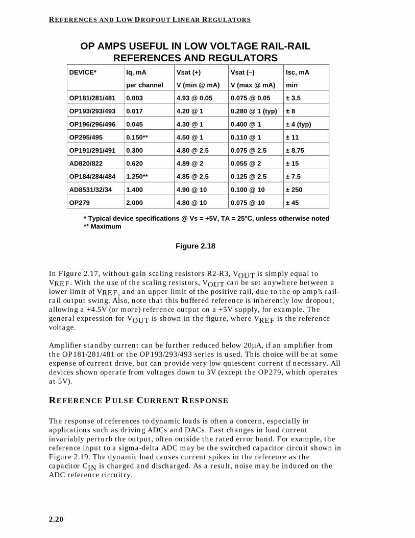
REFERENCES AND LOW DROPOUT LINEAR REGULATORS
2.20
OP AMPS USEFUL IN LOW VOLTAGE RAIL-RAILREFERENCES AND REGULATORS
DEVICE* Iq, mA
per channel
Vsat (+)
V (min @ mA)
Vsat (–)
V (max @ mA)
Isc, mA
min
OP181/281/481 0.003 4.93 @ 0.05 0.075 @ 0.05 ± 3.5
OP193/293/493 0.017 4.20 @ 1 0.280 @ 1 (typ) ± 8
OP196/296/496 0.045 4.30 @ 1 0.400 @ 1 ± 4 (typ)
OP295/495 0.150** 4.50 @ 1 0.110 @ 1 ± 11
OP191/291/491 0.300 4.80 @ 2.5 0.075 @ 2.5 ± 8.75
AD820/822 0.620 4.89 @ 2 0.055 @ 2 ± 15
OP184/284/484 1.250** 4.85 @ 2.5 0.125 @ 2.5 ± 7.5
AD8531/32/34 1.400 4.90 @ 10 0.100 @ 10 ± 250
OP279 2.000 4.80 @ 10 0.075 @ 10 ± 45
* Typical device specifications @ Vs = +5V, TA = 25°C, unless otherwise noted** Maximum
Figure 2.18
In Figure 2.17, without gain scaling resistors R2-R3, VOUT is simply equal toVREF. With the use of the scaling resistors, VOUT can be set anywhere between alower limit of VREF, and an upper limit of the positive rail, due to the op amp’s rail-rail output swing. Also, note that this buffered reference is inherently low dropout,allowing a +4.5V (or more) reference output on a +5V supply, for example. Thegeneral expression for VOUT is shown in the figure, where VREF is the referencevoltage.
Amplifier standby current can be further reduced below 20µA, if an amplifier fromthe OP181/281/481 or the OP193/293/493 series is used. This choice will be at someexpense of current drive, but can provide very low quiescent current if necessary. Alldevices shown operate from voltages down to 3V (except the OP279, which operatesat 5V).
REFERENCE PULSE CURRENT RESPONSE
The response of references to dynamic loads is often a concern, especially inapplications such as driving ADCs and DACs. Fast changes in load currentinvariably perturb the output, often outside the rated error band. For example, thereference input to a sigma-delta ADC may be the switched capacitor circuit shown inFigure 2.19. The dynamic load causes current spikes in the reference as thecapacitor CIN is charged and discharged. As a result, noise may be induced on theADC reference circuitry.

REFERENCES AND LOW DROPOUT LINEAR REGULATORS
2.21
SWITCHED CAPACITOR INPUT OF SIGMA-DELTAADC PRESENTS A DYNAMIC LOAD
TO THE VOLTAGE REFERENCE
+
AGND
VREF IN
CIN~ 10pF
RIN
CEXT
SIGMA-DELTA ADC
Figure 2.19
Although sigma-delta ADCs have an internal digital filter, transients on thereference input can still cause appreciable conversion errors. Thus it is important tomaintain a low noise, transient free potential at the ADC’s reference input. Beaware that if the reference source impedance is too high, dynamic loading can causethe reference input to shift by more than 5mV.
A bypass capacitor on the output of a reference may help it to cope with loadtransients, but many references are unstable with large capacitive loads. Thereforeit is quite important to verify that the device chosen will satisfactorily drive theoutput capacitance required. In any case, the input to references should always bedecoupled - with at least 0.1µF, and with an additional 5-50µF if there is any LFripple on its supply. See Figure 2.12 (again).
Since some references misbehave with transient loads, either by oscillating or bylosing accuracy for comparatively long periods, it is advisable to test the pulseresponse of voltage references which may encounter transient loads. A suitablecircuit is shown in Figure 2.20. In a typical voltage reference, a step change of 1mAproduces the transients shown. Both the duration of the transient, and theamplitude of the ringing increase when a 0.01µF capacitor is connected to thereference output.

REFERENCES AND LOW DROPOUT LINEAR REGULATORS
2.22
MAKE SURE REFERENCE ISSTABLE WITH LARGE CAPACITIVE LOADS
REFERENCEUNDER
TEST
PULSEGENERATOR
VIN
CL RL
1mA to 2mA STEP SCOPE
TOP TRACE: NO LOAD (CL = 0) 50mV/div.
BOTTOM TRACE: CL = 0.01µF200mV/div.
BOTH TRACES: 5µs/div.
Figure 2.20
Where possible, a reference should be designed to drive large capacitive loads. TheAD780 is designed to drive unlimited capacitance without oscillation, it hasexcellent drift and an accurate output, in addition to relatively low powerconsumption. Other references which are useful with output capacitors are theREF19X and AD1582-AD1585 series.
As noted above, reference bypass capacitors are useful when driving the referenceinputs of successive-approximation ADCs. Figure 2.21 illustrates reference voltagesettling behavior immediately following the "Start Convert” command. A smallcapacitor (0.01µF) does not provide sufficient charge storage to keep the referencevoltage stable during conversion, and errors may result. As shown by the bottomtrace, decoupling with a ≥1µF capacitor maintains the reference stability duringconversion.
Where voltage references are required to drive large capacitances, it is also criticallyimportant to realize that their turn-on time will be prolonged. Experiment may beneeded to determine the delay before the reference output reaches full accuracy, butit will certainly be much longer than the time specified on the data sheet for thesame reference in a low capacitance loaded state.

REFERENCES AND LOW DROPOUT LINEAR REGULATORS
2.23
SUCCESSIVE APPROXIMATION ADCs CAN PRESENT ADYNAMIC TRANSIENT LOAD TO THE REFERENCE
AD780
VIN
CB
VREF
SCOPE
SCOPE
START CONVERT
STARTCONVERT
CB = 0.01µF
CB = 0.22µF
CB = 1µF
TOP TRACE VERTICAL SCALE: 5V/div.ALL OTHER VERTICAL SCALES: 5mV/div.HORIZONTAL SCALE: 1µs/div.
SARADC
Figure 2.21
LOW NOISE REFERENCES FOR HIGH RESOLUTION CONVERTERS
High resolution converters (both sigma-delta and high speed ones) can benefit fromrecent improvements in IC references, such as lower noise and the ability to drivecapacitive loads. Even though many data converters have internal references, theperformance of these references is often compromised because of the limitations ofthe converter process. In such cases, using an external reference rather than theinternal one often yields better overall performance. For example, the AD7710-seriesof 22-bit ADCs has a 2.5V internal reference with a 0.1 to 10Hz noise of 8.3µV rms(2600nV/√Hz), while the AD780 reference noise is only 0.67µV rms (200nV/√Hz).The internal noise of the AD7710-series in this bandwidth is about 1.7µV rms. Theuse of the AD780 increases the effective resolution of the AD7710 from about 20.5-bits to 21.5 bits.
Figure 2.22 shows the AD780 used as the reference for the AD7710-series ADCs.The use of the AD780’s optional 3V scaling enhances the dynamic range of the ADC,while lowering overall system noise as described above. In addition, the AD780allows a large decoupling capacitor on its output thereby minimizing conversionerrors due to transients.
There is one possible but yet quite real problem when replacing the internalreference of a converter with a higher precision external one. The converter inquestion may have been trimmed during manufacture to deliver its specifiedperformance with a relatively inaccurate internal reference. In such a case, using amore accurate external reference with the converter may actually introduceadditional gain error! For example, the early AD574 had a guaranteed uncalibratedgain accuracy of 0.125% when using an internal 10V reference (which itself had aspecified accuracy of only ±1%). It is obvious that if such a device, having an internal

REFERENCES AND LOW DROPOUT LINEAR REGULATORS
2.24
reference which is at one end of the specified range, is used with an externalreference of exactly 10V, then its gain will be about 1% in error.
THE AD780 IS IDEAL FOR DRIVINGPRECISION SIGMA-DELTA ADCs
AD780
VIN VO
+
1µF
100nF
+
100µF
AVDDREF IN(+)
REF IN (–)AGND
+5V (ANALOG)
AD77XXΣ∆ Σ∆ ADC
NOTE: ONLY REFERENCECONNECTIONS SHOWN
Figure 2.22
REFERENCES (Voltage References)
1. Bob Widlar, New Developments in IC Voltage Regulators, IEEE Journal of Solid State Circuits, Vol. SC-6, February, 1971.
2. Paul Brokaw, A Simple Three-Terminal IC Bandgap Voltage Reference, IEEE Journal of Solid State Circuits, Vol. SC-9, December, 1974.
3. Paul Brokaw, More About the AD580 Monolithic IC Voltage Regulator, Analog Dialogue, 9-1, 1975.
4. Dan Sheingold, Section 20.2 within Analog-Digital Conversion Handbook, 3d. Edition, Prentice-Hall, 1986.
5. Walt Jung, Build an Ultra-Low-Noise Voltage Reference, Electronic Design Analog Applications Issue, June 24, 1993.
6. Walt Jung, Getting the Most from IC Voltage References, Analog Dialogue, 28-1, 1994, pp. 13-21.

REFERENCES AND LOW DROPOUT LINEAR REGULATORS
2.25
LOW DROPOUT REGULATORS
Walt Jung
INTRODUCTION
Linear IC voltage regulators have long been standard power system building blocks.After an initial introduction in 5 V logic voltage regulator form, they have sinceexpanded into other standard voltage levels spanning from 3 to 24 V, handlingoutput currents from as low as 100 mA (or less) to as high as 5 A (or more). Forseveral good reasons, linear style IC voltage regulators have been valuable systemcomponents since the early days. One reason is the relatively low noisecharacteristic vis-à-vis the switching type of regulator. Others are a low parts countand overall simplicity compared to discrete solutions. But, because of their powerlosses, these linear regulators have also been known for being relatively inefficient.Early generation devices (of which many are still available) required 2V or more ofunregulated input above the regulated output voltage, making them lossy in powerterms.
More recently however, linear IC regulators have been developed with more liberal(i.e., lower) limits on minimum input-output voltage. This voltage, known morecommonly as dropout voltage, has led to what is termed the Low DropOut regulator,or more popularly, the LDO. Dropout voltage (VMIN) is defined simply as thatminimum input-output differential where the regulator undergoes a 2% reduction inoutput voltage. For example, if a nominal 5.0V LDO output drops to 4.9V (-2%)under conditions of an input-output differential of 0.5V, by this definition the LDO’sVMIN is 0.5V.
As will be shown in this section, dropout voltage is extremely critical to a linearregulator stage’s power efficiency. The lower the voltage allowable across a regulatorwhile still maintaining a regulated output, the less power the regulator dissipates asa result. A low regulator dropout voltage is the key to this, as it takes this lowerdropout to maintain regulation as the input voltage lowers. In performance terms,the bottom line for LDOs is simply that more useful power is delivered to the loadand less heat is generated in the regulator. LDOs are key elements of power systemsthat must provide stable voltages from batteries, such as portable computers,cellular phones, etc. This is simply because they maintain their regulated outputdown to lower points on the battery’s discharge curve. Or, within classic mains-powered raw DC supplies, LDOs allow lower transformer secondary voltages,reducing system susceptibility to shutdown under brownout conditions as well asallowing cooler operation.
LINEAR VOLTAGE REGULATOR BASICS
A brief review of three terminal linear IC regulator fundamentals is necessary tounderstanding the LDO variety. As it turns out, almost all LDOs available today, aswell as many of the more general three terminal regulator types, are positive leg,series style regulators. This simply means that they control the regulated voltage

REFERENCES AND LOW DROPOUT LINEAR REGULATORS
2.26
output by means of a pass element which is in series with the positive side ofunregulated input.
This is shown more clearly in Figure 2.23, which is a hookup diagram for ahypothetical three terminal style regulator. To re-iterate what was said earlier inthe chapter about reference ICs, in terms of their basic functionality, many standardvoltage regulator ICs are available in the series three-terminal form as is shownhere (VIN, GND or Common, VOUT).
A BASIC THREE TERMINAL VOLTAGE REGULATOR
THREETERMINAL
REGULATOR
IN OUT
GND
VIN (6V)
VOUT (5V)
COMMON
VMIN = VIN – VOUT = 1V
RL (5ΩΩ)IL
(1A)
IGROUND(1mA)
Figure 2.23
This diagram also allows some statements to be made about power losses in theregulator. There are two components to power which are dissipated in the regulator,one a function of VIN – VOUT and IL, plus a second which is a function of VIN andIground. If we call the total power PD, this then becomes:
( )( ) ( )( )PD VIN VOUT IL VIN Iground= − + .
Obviously, the magnitude of the load current and the regulator dropout voltage bothgreatly influence the power dissipated. However, it is also easy to see that for agiven IL, as the dropout voltage is lowered, the first term of PD is reduced. With anintermediate dropout voltage rating of 1V, a 1A load current will produce 1W of heatin this regulator, which may require a heat sink for continuous operation. It is thisfirst term of the regulator power which usually predominates, at least for loadedregulator conditions.

REFERENCES AND LOW DROPOUT LINEAR REGULATORS
2.27
The second term, being proportional to Iground (typically only 1-2 mA, sometimeseven less) usually only becomes significant when the regulator is unloaded, and theregulator’s quiescent or standby power then produces a constant drain on the sourceVIN.
However, it should be noted that in some types of regulators (notably those whichhave very low β pass devices such as lateral PNP transistors) the Iground currentunder load can actually run quite high. This effect is worst at the onset ofregulation, or when the pass device is in saturation, and can be noted by a suddenIground current “spike”, where the current jumps upward abruptly from a lower lowlevel. All LDO regulators using bipolar transistor pass devices which can besaturated (such as PNPs) can show this effect. It is much less severe in PNPregulators using vertical PNPs (since these have a higher intrinsic β) and doesn’texist to any major extent in PMOS LDOs (since PMOS transistors are controlled byvoltage level, not current).
In the example shown, the regulator delivers 5V × 1A, or 5W to the load. With adropout voltage of 1V, the input power is 6V times the same 1A, or 6W. In terms ofpower efficiency, this can be calculated as:
PEFF(%) 100POUTPIN
= × ,
where POUT and PIN are the total output and input powers, respectively.
In these sample calculations, the relatively small portion of power related to Igroundwill be ignored for simplicity, since this power is relatively small. In an actualdesign, this simplifying step may not be justified.
In the case shown, the efficiency would be 100 × 5/6, or about 83%. But by contrast,if an LDO were to be used with a dropout voltage of 0.1V instead of 1V, the inputvoltage can then be allowed to go as low as 5.1V. The new efficiency for thiscondition then becomes 100 × 5/5.1, or 98%. It is obvious that an LDO canpotentially greatly enhance the power efficiency of linear voltage regulator systems.
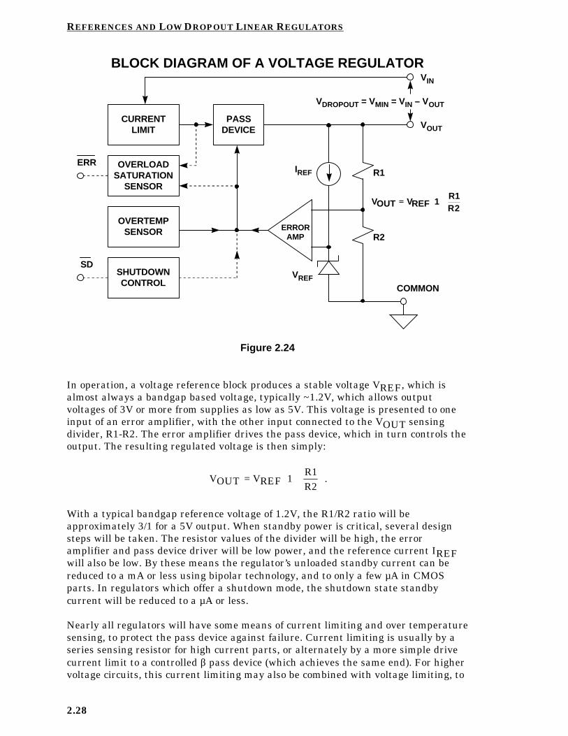
A more detailed look within a typical regulator block diagram reveals a variety ofelements, as is shown in Figure 2.24.
In this diagram virtually all of the elements shown can be considered to befundamentally necessary, the exceptions being the shutdown control and saturationsensor functions (shown dotted). While these are present on many currentregulators, the shutdown feature is relatively new as a standard function, andcertainly isn’t part of standard three-terminal regulators. When present, shutdowncontrol is a logic level controllable input, whereby a digital HIGH (or LO) is definedas regulation active (or vice-versa). The error output, ERR , is useful within asystem to detect regulator overload, such as saturation of the pass device, thermaloverload, etc. The remaining functions shown are always part of an IC powerregulator.
REFERENCES AND LOW DROPOUT LINEAR REGULATORS
2.28
BLOCK DIAGRAM OF A VOLTAGE REGULATOR
CURRENTLIMIT
SHUTDOWNCONTROL
OVERTEMPSENSOR
OVERLOADSATURATION
SENSOR
PASSDEVICE
ERR
SDVREF
IREF
ERRORAMP
R1
R2
VOUT VREFRR
== ++
112
COMMON
VIN
VOUT
VDROPOUT = VMIN = VIN – VOUT
Figure 2.24
In operation, a voltage reference block produces a stable voltage VREF, which isalmost always a bandgap based voltage, typically ~1.2V, which allows outputvoltages of 3V or more from supplies as low as 5V. This voltage is presented to oneinput of an error amplifier, with the other input connected to the VOUT sensingdivider, R1-R2. The error amplifier drives the pass device, which in turn controls theoutput. The resulting regulated voltage is then simply:
VOUT VREF 1R1R2
= +
.
With a typical bandgap reference voltage of 1.2V, the R1/R2 ratio will beapproximately 3/1 for a 5V output. When standby power is critical, several designsteps will be taken. The resistor values of the divider will be high, the erroramplifier and pass device driver will be low power, and the reference current IREFwill also be low. By these means the regulator’s unloaded standby current can bereduced to a mA or less using bipolar technology, and to only a few µA in CMOSparts. In regulators which offer a shutdown mode, the shutdown state standbycurrent will be reduced to a µA or less.
Nearly all regulators will have some means of current limiting and over temperaturesensing, to protect the pass device against failure. Current limiting is usually by aseries sensing resistor for high current parts, or alternately by a more simple drivecurrent limit to a controlled β pass device (which achieves the same end). For highervoltage circuits, this current limiting may also be combined with voltage limiting, to

REFERENCES AND LOW DROPOUT LINEAR REGULATORS
2.29
provide complete load line control for the pass device. All power regulator deviceswill also have some means of sensing over-temperature, usually by means of a fixedreference voltage and a VBE-based sensor monitoring chip temperature. When thedie temperature exceeds a dangerous level (above ~150°C), this can be used toshutdown the chip, by removing the drive to the pass device. In some cases an errorflag output may be provided to warn of this shutdown (and also loss of regulationfrom other sources).
PASS DEVICES AND THEIR ASSOCIATED TRADEOFFS
The discussion thus far has not treated the pass device in any detail. In practice,this major part of the regulator can actually take on quite a number of alternateforms. Precisely which type of pass device is chosen has a major influence on almostall major regulator performance issues. Most notable among these is the dropoutvoltage, VMIN.
Figure 2.25a through 2.25e illustrates a number of pass devices which are usefulwithin voltage regulator circuits, shown in simple schematic form. On the figure isalso listed the salient VMIN for the device as it would typically be used, whichdirectly indicates its utility for use in an LDO. Not shown in these various mini-figures are the remaining circuits of a regulator.
It is difficult to fully compare all of the devices from their schematic representations,since they differ in so many ways beyond their applicable dropout voltages. For thisreason, the chart of Figure 2.26 is useful.
This chart compares the various pass elements in greater detail, allowing easycomparison between the device types, dependent upon which criteria is mostimportant. Note that columns A-E correspond to the schematics of Figure 2.25a-2.25e. Note also that the pro/con comparison items are in relative terms, as opposedto a hard specification limit for any particular pass device type.
For example, it can be seen that the all NPN pass devices of columns A and B havethe attributes of a follower circuit, which allows high bandwidth and providesrelative immunity to cap loading because of the characteristic low ZOUT. However,neither the single NPN nor the Darlington NPN can achieve low dropout, for anyload current. This is because the VBE(s) of the pass device appears in series with theinput, preventing its saturation, and thus setting a VMIN of about 1 or 2V.
By contrast, the inverting mode device connections of both columns C and E do allowthe pass device to be effectively saturated, which lowers the associated voltagelosses to a minimum. This single factor makes these two pass device types optimumfor LDO use, at least in terms of power efficiency.

REFERENCES AND LOW DROPOUT LINEAR REGULATORS
2.30
PASS DEVICES USEFUL IN VOLTAGE REGULATORS
VMIN ≅ ≅ 1VVMIN ≅ ≅ 2V
VMIN ≅ ≅ VCE(SAT) VMIN ≅ ≅ 1.5VVMIN ≅ ≅ RDS(ON) × IL
(a) SINGLE NPN (b) DARLINGTON NPN
(c) SINGLE PNP
(d) PNP/NPN
(e) PMOS
VIN
VOUT
VINVINVIN
VIN
VOUT
VOUT
VOUT
VOUT
Q1
Q2
Q1
Q2
Q1
P1
Figure 2.25
PROS AND CONS OF VOLTAGE REGULATORPASS DEVICES
A
SINGLENPN
B
DARLINGTONNPN
C
SINGLE
PNP
D
PNP/NPN
E
PMOS
VMIN ~ 1V VMIN ~ 2V VMIN ~ 0.1V VMIN ~ 1.5V VMIN ~ RDS(ON)× IL
IL < 1A IL > 1A IL < 1A IL > 1A IL > 1A
Follower Follower Inverter Inverter Inverter
Low ZOUT Low ZOUT High ZOUT High ZOUT High ZOUT
Wide BW Wide BW Narrow BW Narrow BW Narrow BW
CL Immune CL Immune CL Sensitive CL Sensitive CL Sensitive
Figure 2.26

REFERENCES AND LOW DROPOUT LINEAR REGULATORS
2.31
For currents below 1A, either a single PNP or a PMOS pass device is most useful forlow dropout, and they both can achieve a VMIN of 0.1V or less at currents of100mA. The dropout voltage of a PNP will be highly dependent upon the actualdevice used and the operating current, with vertical PNP devices being superior forsaturation losses, as well as minimizing the Iground spike when in saturation.PMOS pass devices offer the potential for the lowest possible VMIN, since the actualdropout voltage will be the product of the device RDS(ON) and IL. Thus a lowRDS(ON) PMOS device can always be chosen to minimize VMIN for a given IL.PMOS pass devices are typically external to the LDO IC, making the IC actually acontroller (as opposed to a complete and integral LDO). PMOS pass devices canallow currents up to several amps or more with very low dropout voltages. ThePNP/NPN connection of column D is actually a hybrid hookup, intended to boost thecurrent of a single PNP pass device. This it does, but it also adds the VBE of theNPN in series (which cannot be saturated), making the net VMIN of the connectionabout 1.5V.
All of the three connections C/D/E have the characteristic of high output impedance,and require an output capacitor for stability. The fact that the output cap is part ofthe regulator frequency compensation is a most basic application point, and onewhich needs to be clearly understood by the regulator user. This factor, denoted by“CL sensitive”, makes regulators using them generally critical as to the exact CLvalue, as well as its ESR (equivalent series resistance). Typically this type ofregulator must be used only with a specific size as well as type of output capacitor,where the ESR is controlled with respect to both time and temperature to fullyguarantee regulator stability. Fortunately, some recent Analog Devices LDO ICcircuit developments have eased this burden on the part of the regulator user agreat deal, and will be discussed below in further detail.
Some examples of standard IC regulator architectures illustrate the points aboveregarding pass devices, and allow an appreciation of regulator developments leadingup to more recent LDO technologies.
The classic LM309 5V/1A three-terminal regulator (see Reference 1) was theoriginator in a long procession of regulators. This circuit is shown in much simplifiedform in Figure 2.27, with current limiting and over temperature details omitted.This IC type is still in standard production today, not just in original form, but infamily derivatives such as the 7805, 7815 etc., and their various low and mediumcurrent alternates. Using a Darlington pass connection for Q18-Q19, the design hasnever been known for low dropout characteristics (~1.5V typical), or for lowquiescent current (~5mA). It is however relatively immune to instability issues, dueto the internal compensation of C1, and the buffering of the emitter follower output.This helps make it easy to apply.
The LM109/309 bandgap voltage reference actually used in this circuit consists of amore involved scheme, as opposed to the basic form which was described with Figure2.3. Resistor R8 drops a PTAT voltage, which drives the Darlington connected erroramplifier, Q9-Q10. The negative TC VBEs of Q9-Q10 and Q12-Q13 are summedwith this PTAT voltage, and this sum produces a temperature-stable 5V outputvoltage. Current buffering of the error amplifier Q10 is provided by PNP Q11, whichdrives the NPN pass devices.

REFERENCES AND LOW DROPOUT LINEAR REGULATORS
2.32
SIMPLIFIED SCHEMATIC OF LM309 FIXED5V/1A THREE-TERMINAL REGULATOR
Q2
Q3
Q4
Q17
Q18
Q19
Q13
Q12
Q5
Q6
Q7
Q8
Q9
Q10
Q11
VIN
VOUT
COMMON
R4
R1
R2
R3
R5 R6
R7
R9
R8
C1
Figure 2.27
Later developments in references and three-terminal regulation techniques led tothe development of the voltage adjustable regulator. The original IC to employ thisconcept was the LM317 (see Reference 2), which is shown in simplified schematicform in Figure 2.28. Note that this design does not use the same ∆VBE form ofreference as in the LM309. Instead, Q17-Q19, etc. are employed as a form of aBrokaw bandgap reference cell (see Figure 2.4 again, and Reference 3).
This adjustable regulator bootstraps the reference cell transistors Q17-Q19 and theerror amplifier transistors Q16-Q18. The output of the error amplifier drivesDarlington pass transistors Q25-Q26, through buffer Q12. The basic reference cellproduces a fixed voltage of 1.25V, which appears between the VOUT and ADJ pinsof the IC as shown. External scaling resistors R1 and R2 set up the desired outputvoltage, which is:
VOUT VREF 1R2R1
50 A R2= +
+ ×µ .
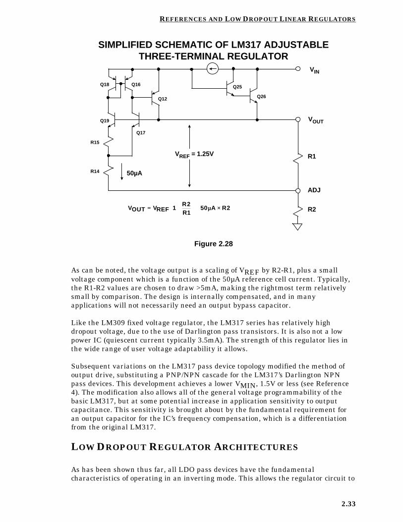
REFERENCES AND LOW DROPOUT LINEAR REGULATORS
2.33
SIMPLIFIED SCHEMATIC OF LM317 ADJUSTABLETHREE-TERMINAL REGULATOR
Q25
VIN
VOUT
Q18
Q19
R15
R14
Q17
Q16
Q12 Q26
R1
R2
ADJ
VREF = 1.25V
50µA
VOUT VREFRR
A R== ++
++ ××121
50 2µµ
Figure 2.28
As can be noted, the voltage output is a scaling of VREF by R2-R1, plus a smallvoltage component which is a function of the 50µA reference cell current. Typically,the R1-R2 values are chosen to draw >5mA, making the rightmost term relativelysmall by comparison. The design is internally compensated, and in manyapplications will not necessarily need an output bypass capacitor.
Like the LM309 fixed voltage regulator, the LM317 series has relatively highdropout voltage, due to the use of Darlington pass transistors. It is also not a lowpower IC (quiescent current typically 3.5mA). The strength of this regulator lies inthe wide range of user voltage adaptability it allows.
Subsequent variations on the LM317 pass device topology modified the method ofoutput drive, substituting a PNP/NPN cascade for the LM317’s Darlington NPNpass devices. This development achieves a lower VMIN, 1.5V or less (see Reference4). The modification also allows all of the general voltage programmability of thebasic LM317, but at some potential increase in application sensitivity to outputcapacitance. This sensitivity is brought about by the fundamental requirement foran output capacitor for the IC’s frequency compensation, which is a differentiationfrom the original LM317.
LOW DROPOUT REGULATOR ARCHITECTURES
As has been shown thus far, all LDO pass devices have the fundamentalcharacteristics of operating in an inverting mode. This allows the regulator circuit to

REFERENCES AND LOW DROPOUT LINEAR REGULATORS
2.34
achieve pass device saturation, and thus low dropout. A by-product of this mode ofoperation is that this type of topology will necessarily be more susceptible tostability issues. These basic points give rise to some of the more difficult issues withregard to LDO performance. In fact, these points influence both the design and theapplication of LDOs to a very large degree, and in the end, determine how they aredifferentiated in the performance arena.
A traditional LDO architecture is shown in Figure 2.29, and is generallyrepresentative of actual parts employing either a PNP pass device as shown, oralternately, a PMOS device. There are both DC and AC design and applicationissues to be resolved with this architecture, which are now discussed.
TRADITIONAL LDO ARCHITECTURE
Q1
Q2 gm
–
+
VREF
R1
R2
CL
ESR
RL
VIN VOUT
CCOMPIGROUND
PNP (OR PMOS)PASS DEVICE
+
Figure 2.29
In DC terms, perhaps the major issue is the type of pass device used, whichinfluences dropout voltage and ground current. If a lateral PNP device is used forQ1, the β will be low, sometimes only on the order or 10 or so. Since Q1 is drivenfrom the collector of Q2, the relatively high base current demanded by a lateral PNPresults in relatively high emitter current in Q2, or a high Iground. For a typicallateral PNP based regulator operating with a 5V/150mA output, Iground will betypically ~18mA, and can be as high as 40mA. To compound the problem of highIground in PNP LDOs, there is also the “spike” in Iground, as the regulator isoperating within its dropout region. Under such conditions, the output voltage is outof tolerance, and the regulation loop forces higher drive to the pass device, in anattempt to maintain loop regulation. This results in a substantial spike upward inIground, which is typically internally limited by the regulator’s saturation controlcircuits.
PMOS pass devices do not demonstrate a similar current spike in Iground, sincethey are voltage controlled. But, while devoid of the Iground spike, PMOS pass

REFERENCES AND LOW DROPOUT LINEAR REGULATORS
2.35
devices do have some problems of their own. Problem number one is that highquality, low RON, low threshold PMOS devices generally aren’t compatible withmany IC processes. This makes the best technical choice for a PMOS pass device anexternal part, driven from the collector of Q2 in the figure. This introduces the term“LDO controller”, where the LDO architecture is completed by an external passdevice. While in theory NMOS pass devices would offer lower RON choice options,they also demand a boosted voltage supply to turn on, making them impractical fora simple LDO. PMOS pass devices are widely available in low both RON and lowthreshold forms, with current levels up to several amperes. They offer the potentialof the lowest dropout of any device, since dropout can always be lowered by picking alower RON part.
The dropout voltage of lateral PNP pass devices is reasonably good, typically around300mV at 150mA, with a maximum of 600mV. These levels are howeverconsiderably bettered in regulators using vertical PNPs, which have a typical β of~150 at currents of 200mA. This leads directly to an Iground of 1.5mA at the 200mAoutput current. The dropout voltage of vertical PNPs is also an improvement vis-à-vis that of the lateral PNP regulator, and is typically 180mV at 200mA, with amaximum of 400mV.
There are also major AC performance issues to be dealt with in the LDOarchitecture of Fig. 2.29. This topology has an inherently high output impedance,due to the operation of the PNP pass device in a common-emitter (or common-sourcewith a PMOS device) mode. In either case, this factor causes the regulator to appearas a high source impedance to the load.
The internal compensation capacitor of the regulator, CCOMP, forms a fixedfrequency pole, in conjunction with the gm of the error amplifier. In addition, loadcapacitance CL forms an output pole, in conjunction with RL. This particular pole,because it is a second (and sometimes variable) pole of a two-pole system, is thesource of a major LDO application problem. The CL pole can strongly influence theoverall frequency response of the regulator, in ways that are both useful as well asdetrimental. Depending upon the relative positioning of the two poles in thefrequency domain, along with the relative value of the ESR of capacitor CL, it isquite possible that the stability of the system can be compromised for certaincombinations of CL and ESR. Note that CL is shown here as a real capacitor, whichis actually composed of a pure capacitance plus the series parasitic resistance ESR.
Without a heavy duty exercise into closed-loop stability analysis, it can safely besaid that LDOs, like other feedback systems, need to satisfy certain basic stabilitycriteria. One of these is the gain-versus-frequency rate-of-change characteristic inthe region approaching the system’s unity loop gain crossover point. For the systemto be closed loop stable, the phase shift must be less than 180° at the point of unitygain. In practice, a good feedback design needs to have some phase margin,generally 45° or more to allow for various parasitic effects. While a single polesystem is intrinsically stable, two pole systems are not necessarily so—they may infact be stable, or they may also be unstable. Whether or not they are stable for agiven instance is highly dependent upon the specifics of their gain-phasecharacteristics.

REFERENCES AND LOW DROPOUT LINEAR REGULATORS
2.36
If the two poles of such a system are widely separated in terms of frequency,stability may not be a serious problem. The emitter-follower output of a classicregulator like the LM309 is an example with widely separated pole frequencies, asthe very low ZOUT of the NPN follower pushes the output pole due to loadcapacitance far out in frequency, where it does little harm. The internalcompensation capacitance (C1 of Fig. 2.27, again) then forms part of a dominantpole, which reduces loop gain to below unity at the much higher frequencies wherethe output pole does occur. Thus stability is not necessarily compromised by loadcapacitance in this type of regulator.
Figure 2.30 summarizes the various DC and AC design issues of LDOs.
DC AND AC DESIGN ISSUESIN LOW DROPOUT REGULATORS
n Lateral PNP Pass Device:
High IGROUND
n Vertical PNP Pass Device:
Low IGROUND
Low VMIN
n PMOS Pass Device:
Lowest IGROUND Variation
Low VMIN
Ampere Level OutputCurrents
n Two Pole CompensationSystem
n CL ESR Critical to Stability
n Requires Large CL
n Requires"Zoned" CL ESR(Max/Min ESR Limits Over Timeand Temperature)
DC AC
Figure 2.30
By their nature however, LDOs simply can’t afford the luxury of emitter followeroutputs, they must instead operate with pass devices capable of saturation. Thus,given the existence of two or more poles (one or more internal and a second formedby external loading) there is the potential for the cumulative gain-phase to add in aless than satisfactory manner. The potential for instability under certain outputloading conditions is, for better or worse, a fact-of-life for most LDO topologies.
However, the output capacitor which gives rise to the instability can, for certaincircumstances, also be the solution to the same instability. This seeminglyparadoxical situation can be appreciated by realizing that almost all practicalcapacitors are actually as shown in Fig. 2.29, a series combination of the capacitanceCL and a parasitic resistance, ESR. While load resistance RL and CL do form a pole,CL and its ESR also form a zero. The effect of the zero is to mitigate the de-stabilizing effect of CL for certain conditions. For example, if the pole and zero in

REFERENCES AND LOW DROPOUT LINEAR REGULATORS
2.37
question are appropriately placed in frequency relative to the internal regulatorpoles, some of the deleterious effects can be made to essentially cancel, leaving littleor no problematic instability (see Reference 5). The basic problem with this setup issimply that the capacitor’s ESR, being a parasitic term, is not at all well controlled.As a result, LDOs which depend upon output pole-zero compensation schemes mustvery carefully limit the capacitor ESR to certain zones, such as shown by Figure2.31.
ZONED LOAD CAPACITOR ESR CAN MAKEAN LDO APPLICATIONS NIGHTMARE
0.1
1
10
100
0 1000IOUT (mA)
UNSTABLE
STABLE
UNSTABLE
CAPACITORESR (ΩΩ)
Figure 2.31
A zoned ESR chart such as this is meant to guide the user of an LDO in picking anoutput capacitor which confines ESR to the stable region, i.e., the central zone, forall operating conditions. Note that this generic chart is not intended to portray anyspecific device, just the general pattern. Unfortunately, capacitor facts of life makesuch data somewhat limited in terms of the real help it provides. Bearing in mindthe requirements of such a zoned chart, it effectively means that general purposealuminum electrolytic are prohibited from use, since they deteriorate in terms ofESR at cold temperatures. Very low ESR types such as OS-CON or multi-layerceramic units have ESRs which are too low for use. While they could in theory bepadded up into the stable zone with external resistance, this would hardly be apractical solution. This leaves tantalum types as the best all around choice for LDOoutput use. Finally, since a large capacitor value is likely to be used to maximizestability, this effectively means that the solution for an LDO such as Fig. 2.29 mustuse a more expensive and physically large tantalum capacitor. This is not desirableif small size is a major design criteria.

REFERENCES AND LOW DROPOUT LINEAR REGULATORS
2.38
THE anyCAPTM LOW DROPOUT REGULATOR FAMILY
Some novel modifications to the basic LDO architecture of Fig. 2.29 allow majorimprovements in terms of both DC and AC performance. These developments areshown schematically in Figure 2.32, which is a simplified diagram of the AnalogDevices ADP330X series LDO regulator family. These regulators are also known asthe anyCAPTM family, so named for their relative insensitivity to the outputcapacitor in terms of both size and ESR. They are available in power efficientpackages such as the Thermal Coastline (discussed below), in both stand-alone LDOand LDO controller forms, and also in a wide span of output voltage options.
ADP330X anyCAPTM TOPOLOGY FEATURES IMPROVEDDC & AC PERFORMANCE OVER TRADITIONAL LDOs
NONINVERTINGWIDEBAND
DRIVER
Q1
PTATVOSgm
+
–
VIN VOUT
CCOMP
R4
R3 D1 R1||R2
×1
R1
R2
RL
CL
GND
IPTAT
Figure 2.32
Design Features Related to DC Performance
One of the key differences in the ADP330X series is the use of a high gain verticalPNP pass device, with all of the advantages described above with Figs. 2.29 and2.30 (also, see Reference 6). This allows the typical dropout voltages for the series tobe on the order of 1mV/mA for currents of 200mA or less.
It is important to note that the topology of this LDO is distinctly different from thatof the generic form in Fig. 2.29, as there is no obvious VREF block. The reason forthis is the fact that the ADP330X series uses what is termed a “merged” amplifier-reference design. The operation of the integral amplifier and reference schemeillustrated in Fig. 2.32 can be described as follows.

REFERENCES AND LOW DROPOUT LINEAR REGULATORS
2.39
In this circuit, VREF is defined as a reference voltage existing at the output of a zeroimpedance divider of ratio R1/R2. In the figure, this is depicted symbolically by the(dotted) unity gain buffer amplifier fed by R1/R2, which has an output of VREF.This reference voltage feeds into a series connection of (dotted) R1||R2, then actualcomponents D1, R3, R4, etc.
The error amplifier, shown here as a gm stage, is actually a PNP input differentialstage with the two transistors of the pair operated at different current densities, soas to produce a predictable PTAT offset voltage. Although shown here as a separateblock VOS, this offset voltage is inherent to a bipolar pair for such operatingconditions. The PTAT VOS causes a current IPTAT to flow in R4, which is simply:
IPTATVOSR4
= .
Note that this current also flows in series connected R4, R3, and the Theveninresistance of the divider, R1||R2, so:
( )VPTAT IPTAT R3 + R4 + R1||R2= .
The total voltage defined as VREF is the sum of two component voltages:
VREF VPTAT VD1= + ,
where the IPTAT scaled voltages across R3, R4, and R1||R2 produce a net PTATvoltage VPTAT, and the diode voltage VD1 is a CTAT voltage. As in a standardbandgap reference, the PTAT and CTAT components add up to a temperature stablereference voltage of 1.25V. In this case however, the reference voltage is not directlyaccessible, but instead it exists in the virtual form described above. It acts as itwould be seen at the output of a zero impedance divider of a numeric ratio of R1/R2,which is then fed into the R3-D1 series string through a Thevenin resistance ofR1||R2 in series with D1.
With the closed loop regulator at equilibrium, the voltage at the virtual referencenode will be:
VREF VOUTR2
R1 + R2=
.
REFERENCES AND LOW DROPOUT LINEAR REGULATORS
2.40
With minor re-arrangement, this can be put into the standard form to describe theregulator output voltage, as:
VOUT VREF 1R1R2
= +
.
In the various devices of the ADP330X series, the R1-R2 divider is adjusted toproduce standard output voltages of 2.7, 3.0, 3.2, 3.3, and 5.0V.
As can be noted from this discussion, unlike a conventional reference setup, there isno power wasting reference current such as used in a conventional regulatortopology (IREF of Fig. 2.24). In fact, the Fig. 2.32 regulator behaves as if the entireerror amplifier has simply an offset voltage of VREF volts, as seen at the output of aconventional R1-R2 divider.
Design Features Related to AC Performance
While the above described DC performance enhancements of the ADP330X seriesare worthwhile, the most dramatic improvements come in areas of AC relatedperformance. These improvements are in fact the genesis of the anyCAPTM seriesname.
Capacitive loading and the potential instability it brings is a major deterrentto easily applying LDOs. While low dropout goals prevent the use of emitter followertype outputs, and so preclude their desirable buffering effect against cap loading,there is an alternative technique of providing load immunity. One method ofproviding a measure of insusceptibility against variation in a particular amplifierresponse pole is called pole splitting (see Reference 8). It refers to an amplifiercompensation method whereby two response poles are shifted in such a way so as tomake one a dominant, lower frequency pole. In this manner the secondary pole(which in this case is the CL related output pole) becomes much less of a majorcontributor to the net AC response. This has the desirable effect of greatly de-sensitizing the amplifier to variations in the output pole.
A Basic Pole-Splitting Topology
A basic LDO topology with frequency compensation as modified for pole splitting isshown in Figure 2.33. Here the internal compensation capacitor CCOMP isconnected as an integrating capacitor, around pass device Q1 (C1 is the pass deviceinput capacitance). While it is true that this step will help immunize the regulator tothe CL related pole, it also has a built in fatal flaw. With CCOMP connected directlyto the Q1 base as shown, the line rejection characteristics of this setup will be quitepoor. In effect, when doing it this way one problem (CL sensitivity) will be exchangedfor another (poor line rejection).

REFERENCES AND LOW DROPOUT LINEAR REGULATORS
2.41
THE SOLUTION TO CL SENSITIVITY:POLE SPLIT COMPENSATION
(WRONG WAY EXAMPLE!)
Q1
gm+
–
C1CCOMP
VREF
+
R1
R2
CL
ESRRL
VIN VOUT
Figure 2.33
The anyCAPTM Pole-Splitting Topology
Returning to the anyCAPTM series topology, (Fig. 2.32, again) it can be noted that inthis case CCOMP is isolated from the pass device’s base (and thus input ripplevariations), by the wideband non-inverting driver. But insofar as frequencycompensation is concerned, because of this buffer’s isolation, CCOMP still functionsas a modified pole splitting capacitor (see Reference 9), and it does provide thebenefits of a buffered, CL independent single-pole response. The regulator’sfrequency response is dominated by the internal compensation, and becomesrelatively immune to the value and ESR of load capacitor CL. Thus the nameanyCAPTM for the series is apt, as the design is tolerant of virtually any outputcapacitor type.
The benefits of the anyCAPTM topology are summarized by Figure 2.34. As can benoted, CL can be as low as 0.47µF, and it can also be a multi-layer ceramic capacitor(MLCC) type. This allows a very small physical size for the entire regulationfunction, such as when a SOT-23 packaged anyCAPTM LDO is used, for example theADP3300 device. Because of the in-sensitivity to CL, the designer needn’t worryabout such things as ESR zones, and can better concentrate on the system aspects ofthe regulator application.

REFERENCES AND LOW DROPOUT LINEAR REGULATORS
2.42
BENEFITS OF anyCAPTM
LDO TOPOLOGY
n Internal CCOMP Dominates Response Rolloff
n CL Can Range from 0.47µF(min) to Infinity
n Low and Ultra-Low CL ESR is OK
n MLCC Types for CL Work, is Physically Smallest Solution
n No ESR Exclusion Zones
n Fast Load Transient Response and Good Line Rejection
Figure 2.34
The anyCAPTM LDO series devices
The major specifications of the anyCAPTM series of LDO regulators are summarizedin Figure. 2.35. The devices include both single and dual output parts, with currentcapabilities ranging from 50 to 200mA. Rather than separate individualspecifications for output tolerance, line and load regulation, plus temperature, theanyCAPTM series devices are rated simply for a combined total accuracy figure. Thisaccuracy is either 0.8% at 25°C, or 1.4% over the temperature range with the deviceoperating over an input range of VOUT +0.3 (or 0.5V), up to 12V. With totalaccuracy being covered by one clear specification, the designer can then achieve ahigher degree of confidence. It is important to note that this method of specificationalso includes operation within the regulator dropout range (unlike some LDO partsspecified for higher input-output voltage difference conditions).
anyCAPTM SERIES LDO REGULATOR DEVICES
PartNumber
VMIN @ IL(V, typ/max)
IL(mA)
Accuracy
(±±% @ 25°°C /
±±% Full)
Package
(All SO-8 areThermal
coastline)
Comment
(Singles haveNR, SD, ERR;Dual no NR)
ADP3300 0.08 / 0.17 50 0.8 / 1.4 SOT-23-6 Single
ADP3301 0.10 / 0.2 100 0.8 / 1.4 SO-8 Single
ADP3302 0.10 / 0.2 100 0.8 / 1.4 SO-8 Dual
ADP3303 0.18 / 0.4 200 0.8 / 1.4 SO-8 Single
ADP3307 0.13 / 0.22 100 0.8 / 1.4 SOT-23-6 Single
Figure 2.35

REFERENCES AND LOW DROPOUT LINEAR REGULATORS
2.43
Functional Diagram and Basic 50 mA LDO Regulator
A functional diagram common to the various devices of the ADP330X series LDOregulators is shown by Figure 2.36. Operation of the various pins and internalfunctions is discussed below.
anyCAPTM SERIES LDO REGULATORSFUNCTIONAL DIAGRAM
Q1
gm+
–
R1
R2
DRIVER
THERMALPROTECTION
+
BANDGAPREF
CC
Q2
IN
ERR
SD
OUT
GND
Figure 2.36
In application, the use of the anyCAPTM series of LDOs is simple, as shown by abasic 50mA ADP3300 regulator, in Figure 2.37. This circuit is a general one, toillustrate points common to the entire device series. The ADP3300 is a basic LDOregulator device, designed for fixed output voltage applications while operating fromsources over a range of 3 to 12V and a temperature range of –40 to +85°C. Theactual ADP3300 device ordered would be specified as ADP3300ART-YY, where the“YY” is a voltage designator suffix such as 2.7, 3, 3.2, 3.3, or 5, for those respectivevoltages. The “ART” portion of the part number designates the SOT23 6-leadpackage. The example circuit shown produces 5.0V with the use of the ADP3300-5.
In operation, the circuit will produce its rated 5V output for loads of 50mA or less,and for input voltages above 5.3V (VOUT + 0.3V), when the shutdown input is in aHIGH state. This can be accomplished either by a logic HIGH control input to theSD pin, or by simply tying this pin to VIN. When SD is LOW (or tied to ground), theregulator shuts down, and draws a quiescent current of 1µA or less.

REFERENCES AND LOW DROPOUT LINEAR REGULATORS
2.44
A BASIC ADP3300 50mALDO REGULATOR CIRCUIT
5
3 1
6
4
2
ADP3300-5
IN NR
OUT
ERRGNDSD
C10.47µF
C20.47µF
C30.01µF
R1330kΩΩ
OFF
ON
VIN
VOUT = 5V
Figure 2.37
The ADP3300 and other anyCAPTM series devices maintain regulation over a widerange of load, input voltage and temperature conditions. However, when theregulator is overloaded or entering the dropout region (for example, by a reductionin the input voltage) the open collector ERR pin becomes active, by going to a LOWor conducting state. Once set, the ERR pin’s internal hysteresis keeps the outputlow, until some margin of operating range is restored. In the circuit of Fig. 2.37, R1is a pullup resistor for the ERR output, EOUT. This resistor can be eliminated ifthe load being driven provides a pullup current.
The ERR function can also be activated by the regulator’s over temperatureprotection circuit, which trips at 165°C. These internal current and thermal limitsare intended to protect the device against accidental overload conditions. For normaloperation, device power dissipation should be externally limited by means of heatsinking, air flow, etc. so that junction temperatures will not exceed 125°C.
A capacitor, C3, connected between pins 2 and 4, can be used for an optional noisereduction (NR) feature. This is accomplished by AC-bypassing a portion of theregulator’s internal scaling divider, which has the effect of reducing the output noise~10 dB. When this option is exercised, only low leakage 10 -100nF capacitors shouldbe used. Also, input and output capacitors should be changed to 1 and 4.7µF valuesrespectively, for lowest noise and the best overall performance. Note that the noisereduction pin is internally connected to a high impedance node, so connections to itshould be carefully done to avoid noise. PC traces and pads connected to this pinshould be as short and small as possible.

REFERENCES AND LOW DROPOUT LINEAR REGULATORS
2.45
LDO Regulator Thermal Considerations
To determine a regulator’s power dissipation, calculate it as follows:
( )( ) ( )( )PD VIN VOUT IL VIN Iground= − + ,
where IL and Iground are load and ground current, and VIN and VOUT are theinput and output voltages respectively. Assuming IL= 50mA, Iground = 0.5mA, VIN= 8V, and VOUT = 5V, the device power dissipation is:
PD = (8 – 5)(0.05) + (8)(0.0005)= 0.150 + .004 = 0.154 W.
To determine the regulator’s temperature rise, ∆T, calculate it as follows:
∆T = TJ – TA = PD × θJA = 0.154W × 165°C/W = 25.4°C.
With a maximum junction temperature of 125°C, this yields a calculated maximumsafe ambient operating temperature of 125 – 25.4°C, or just under 100°C. Since thistemperature is in excess of the device’s rated temperature range of 85°C, the devicewill then be operated conservatively at an 85°C (or less) maximum ambienttemperature.
These general procedures can be used for other devices in the series, substitutingthe appropriate θJA for the applicable package, and applying the remainingoperating conditions. For reference, a complete tutorial section on thermalmanagement is contained in Chapter 8.
In addition, layout and PCB design can have a significant influence on the powerdissipation capabilities of power management ICs. This is due to the fact that thesurface mount packages used with these devices rely heavily on thermallyconductive traces or pads, to transfer heat away from the package. Appropriate PClayout techniques should then be used to remove the heat due to device powerdissipation. The following general guidelines will be helpful in designing a boardlayout for lowest thermal resistance in SOT-23 and SO-8 packages:
1. PC board traces with large cross sectional areas remove more heat. For optimumresults, use large area PCB patterns with wide and heavy (2 oz.) copper traces,placed on the uppermost side of the PCB.
2. Electrically connect dual VIN and VOUT pins in parallel, as well as to the
corresponding VIN and VOUT large area PCB lands. 3. In cases where maximum heat dissipation is required, use double-sided copper
planes connected with multiple vias. 4. Where possible, increase the thermally conducting surface area(s) openly exposed
to moving air, so that heat can be removed by convection (or forced air flow, ifavailable).
5. Do not use solder mask or silkscreen on the heat dissipating traces, as they
increase the net thermal resistance of the mounted IC package.

REFERENCES AND LOW DROPOUT LINEAR REGULATORS
2.46
A real life example visually illustrates a number of the above points far better thanwords can do, and is shown in Figure 2.38, a photo of the ADP3300 1.5" squareevaluation PCB. The boxed area on the board represents the actual active circuitarea.
ADP3300 EVALUATION BOARD:CAPACITOR SIZE CAN MAKE A DIFFERENCE!
10µF / 16VTANTALUM CAPACITOR
(KEMET T491C SERIES)
TOTALBOARD SIZE:
1.5" X 1.5"
Figure 2.38
In this figure, a large cross section conductor area can be seen associated with pin 4and VOUT, the large “U” shaped trace at the lower part within the boxed outline.
Also, the effect of the anyCAPTM design on capacitor size can be noted from the tinysize of the C1 and C2 0.47µF input and output capacitors, near the upper left of theboxed area. For comparison purposes, a 10µF/16V tantalum capacitor (KemetT491C-series) is also shown outside the box, as it might be used on a moreconventional LDO circuit. It is several times the size of output capacitor C2.
Recent developments in packaging have led to much improved thermal performancefor power management ICs. The anyCAPTM LDO regulator family capitalizes on thismost effectively, using a thermally improved leadframe as the basis for all 8 pindevices. This package is called a “Thermal Coastline” design, and is shown inFigure. 2.39. The foundation of the improvement in heat transfer is related to twokey parameters of the leadframe design, distance and width. The payoff comes inthe reduced thermal resistance of the leadframe based on the Thermal Coastline,only 90°C/W versus 160°C/W for a standard SO-8 package. The increased dissipationof the Thermal Coastline allows the anyCAPTM series of SO-8 regulators to supportmore than one watt of dissipation at 25°C.

REFERENCES AND LOW DROPOUT LINEAR REGULATORS
2.47
anyCAPTM SERIES REGULATORS IN SO-8 USETHERMAL COASTLINE PACKAGES
1
2
3
4 5
6
7
8
THERMAL COASTLINE SOIC
θJA = 90 ºC/W
1
2
3
4 5
6
7
8
STANDARD LEADFRAME SOIC
θJA = 160 ºC/W
Figure 2.39
Additional insight into how the new leadframe increases heat transfer can beappreciated by Figure. 2.40. In this figure, it can be noted how the spacing of theThermal Coastline paddle and leads shown on the right is reduced, while the widthof the lead ends are increased, versus the standard leadframe, on the left.
DETAILS OF THERMAL COASTLINE PACKAGE
Lead 1
Lead 2Paddle
Center ofPackage
THERMAL COASTLINE FRAME
Lead 1
Lead 2 Paddle
STANDARD FRAME
Width of adjoiningfaces increased byfactor of 2 to 2.5
Face-to-face distance,from lead to paddlereduced by a factor of1.5 to 2
Center ofPackage
Figure 2.40

REFERENCES AND LOW DROPOUT LINEAR REGULATORS
2.48
LDO REGULATOR CONTROLLERS
To complement the anyCAPTM series of standalone LDO regulators, there is also theLDO regulator controller. The regulator controller IC picks up where the standaloneregulator IC is no longer useful in either load current or power dissipation terms,and uses an external PMOS FET for the pass device. The ADP3310 is a basic LDOregulator controller device, designed for fixed output voltage applications whileoperating from sources over a range of 3.8 to 15V and a temperature range of –40 to+85°C. The actual ADP3310 device ordered would be specified as ADP3310AR-YY,where the “YY” is a voltage designator suffix such as 2.8, 3, 3.3, or 5, for thoserespective voltages. The “AR” portion of the part number designates the SO-8Thermal Coastline 8-lead package. A summary of the main features of the ADP3310device is listed in Figure 2.41.
anyCAPTM ADP3310 LDOREGULATOR CONTROLLER FEATURES
n Controller drives external PMOS power FETs
u User FET choice determines IL and VMIN performance
u Small, 2 chip regulator solution handles up to 10A
n Advantages compared to integrated solutions
u High accuracy (1.5%) fixed voltages; 2.8, 3, 3.3, or 5Vu User flexibility (selection of FET for performance)u Small footprint with anyCAPTM controller and SMD FETu Kelvin output sensing possibleu Integral, low-loss current limit sensing for protection
Figure 2.41
Regulator Controller Differences
An obvious basic difference of the regulator controller versus a stand alone regulatoris the removal of the pass device from the regulator chip. This design step has bothadvantages and disadvantages. A positive is that the external PMOS pass devicecan be chosen for the exact size, package, current rating and power handling whichis most useful to the application. This approach allows the same basic controller ICto be useful for currents of several hundred mA to more than 10A, simply by choiceof the FET. Also, since the regulator controller IC’s Iground of 800µA results is verylittle power dissipation, its thermal drift will be enhanced. On the downside, thereare two packages now used to make up the regulator function. And, current limiting(which can be made completely integral to a standalone IC LDO regulator) is now afunction which must be split between the regulator controller IC and an externalsense resistor. This step also increases the dropout voltage of the LDO regulatorcontroller somewhat, by about 50mV.

REFERENCES AND LOW DROPOUT LINEAR REGULATORS
2.49
A functional diagram of the ADP3310 regulator controller is shown in Figure 2.42.The basic error amplifier, reference and scaling divider of this circuit are similar tothe standalone anyCAPTM regulator, and will not be described in detail. Theregulator controller version does share the same cap load immunity of thestandalone versions, and also has a shutdown function, similarly controlled by theEN (enable) pin.
The main differences in the regulator controller IC architecture is the bufferedoutput of the amplifier, which is brought out on the GATE pin, to drive the externalPMOS FET. In addition, the current limit sense amplifier has a built in 50mVthreshold voltage, and is designed to compare the voltage between the VIN and ISpins. When this voltage exceeds 50mV, the current limit sense amplifier takes overcontrol of the loop, by shutting down the error amplifier and limiting output currentto the preset level.
FUNCTIONAL BLOCK DIAGRAM OFanyCAPTM SERIES LDO REGULATOR CONTROLLER
BIAS
VREF
+
–
SOURCE(IS)
GATE
VOUT
EN
–
+
VIN
GND
50mV
Figure 2.42
A Basic 5V/1A LDO Regulator Controller
An LDO regulator controller is easy to use, since a PMOS FET, a resistor and tworelatively small capacitors (one at the input, one at the output) is all that is neededto form an LDO regulator. The general configuration is shown by Figure 2.43, anLDO suitable as a 5V/1A regulator operating from a VIN of 6V, using the ADP3310-5 controller IC.
This regulator is stable with virtually any good quality output capacitor used for CL(as is true with the other anyCAPTM devices). The actual CL value required and itsassociated ESR depends on the gm and capacitance of the external PMOS device. In

REFERENCES AND LOW DROPOUT LINEAR REGULATORS
2.50
general, a 10µF capacitor at the output is sufficient to ensure stability for loadcurrents up to 10A. Larger capacitors can also be used, if high output surge currentsare present. In such cases, low ESR capacitors such as OS-CON electrolytics arepreferred, because they offer lowest ripple on the output. For less demandingrequirements, a standard tantalum or aluminum electrolytic can be adequate. Whenan aluminum electrolytic is used, it should be qualified for adequate performanceover temperature. The input capacitor, CIN, is only necessary when the regulator isseveral inches or more distant from the raw DC filter capacitor. However, since it isa small type, it is usually prudent to use it in most instances, located close to theVIN pin of the regulator.
A BASIC ADP3310 PMOS FET 1A LDOREGULATOR CONTROLLER CIRCUIT
+
+
RS50mΩΩVIN = 6V MIN VOUT = 5V @ 1A
VIN
EN
IS GATE
VOUT
ADP3310-5
GND
NDP6020P OR NDB6020P (FAIRCHILD)
CIN1µF
CL10µF
Figure 2.43
Selecting the Pass Device
The type and size of the pass transistor are determined by a set of requirements forthreshold voltage, input-output voltage differential, load current, power dissipation,and thermal resistance. An actual PMOS pass device selected must satisfy all ofthese electrical requirements, plus physical and thermal parameters. There are anumber of manufacturers offering suitable devices in packages ranging from SO-8up through TO-220 in size.
To ensure that the maximum available drive from the controller will adequatelydrive the FET under worst case conditions of temperature range and manufacturingtolerances, the maximum drive from the controller (VGS(DRIVE)) to the pass devicemust be determined. This voltage is calculated as follows:
( )( )VGS(DRIVE) VIN VBE IL(MAX) RS= − − ,

REFERENCES AND LOW DROPOUT LINEAR REGULATORS
2.51
where VIN is the minimum input voltage, IL(MAX) is the maximum load current,RS the sense resistor, and VBE is a voltage internal to the ADP3310 (~ 0.5 @ hightemp, 0.9 cold, and 0.7V at room temp). Note that since IL(MAX) × RS will be nomore than 75mV, and VBE at cold temperature ≅0.9V, this equation can be furthersimplified to:
VGS(DRIVE) VIN 1V≅ − .
In the Figure 2.43 example, VIN = 6V and VOUT = 5V, so VGS(DRIVE) is 6 – 1 =5V.
It should be noted that the above two equations apply to FET drive voltages whichare less than the typical gate-to-source clamp voltage of 8V (built into the ADP3310,for the purposes of FET protection).
An overall goal of the design is to then select an FET which will have an RDS(ON)sufficiently low so that the resulting dropout voltage will be less than VIN – VOUT,which in this case is 1V. For the NDP6020P used in Fig. 2.43 (see Reference 10),this device achieves an RDS(ON) of 70 milliohms (max) with a VGS of 2.7V, avoltage drive appreciably less than the ADP3310’s VGS(DRIVE) of 5V. The dropoutvoltage VMIN of this regulator configuration is the sum of two series voltage drops,the FET’s drop plus the drop across RS, or:
( )VMIN = IL(MAX) RDS(ON) + RS .
In the design here, the two resistances are roughly comparable to one another, sothe net VMIN will be 1A × (50+70 milliohms) = 120mV.
For a design safety margin, use a FET with a rated VGS at the required RDS, witha substantial headroom between the applicable ADP3310 VGS(DRIVE) and theapplicable VGS rating for the FET. In the case here, there is ample margin, with 5Vof drive and a VGS of 2.7V. It should be borne in mind that the FET’s VGS andRDS(ON) will change over temperature, but for the NDP6020P device even thesevariations and a VGS of 4.5V are still possible with the circuit as shown. With arated minimum DC input of 6V, this means that the design is conservative with 5Voutput. In practice, the circuit will typically operate with input voltage minimumson the order of VOUT plus the dropout of 120mV, or ~ 5.12V. Since the NDP6020Pis also a fairly low threshold device, it will typically operate at lower output voltages,down to about 3V.
In the event the output is shorted to ground, the pass device chosen must be able toconduct the maximum short circuit current, both instantaneously and longer term.
Thermal Design
The maximum allowable thermal resistance between the FET junction and thehighest expected ambient temperature must be taken into account, to determine thetype of FET package and heat sink used (if any).

REFERENCES AND LOW DROPOUT LINEAR REGULATORS
2.52
Whenever possible to do so reliably, the FET pass device can be directly mounted tothe PCB, and the available PCB copper lands used as an effective heat sink. Thisheat sink philosophy will likely be adequate when the power to be dissipated in theFET is on the order of 1-2W or less. Note that the very nature of an LDO helps thistype of design immensely, as the lower voltage drop across the pass device reducesthe power to be dissipated. Under normal conditions for example, Q1 of Figure 2.43dissipates less than 1W at a current of 1A, since the drop across the FET is less than1V.
To use PCB lands as effective heat sinks with SO-8 and other SMD packages, thepass device manufacturer’s recommendations for the lowest θJA mounting should befollowed (see References 11 and 12). In general these suggestions will likely parallelthe 5 rules noted above, under “LDO regulator thermal considerations” for SO-8 andSOT-23 packaged anyCAPTM LDOs. For lowest possible thermal resistance, alsoconnect multiple FET pins together, as follows:
Electrically connect multiple FET source and drain pins in parallel, as well as to thecorresponding RS and VOUT large area PCB lands.
Using 2 oz. copper PCB material and one square inch of copper PCB land area as aheatsink, it is possible to achieve a net thermal resistance, θJA, for mounted SO-8devices on the order of 60°C/W or less. Such data is available for SO-8 power FETs(see Reference 11). There are also a variety of larger packages with lower thermalresistance than the SO-8, but still useful with surface mount techniques. Examplesare the DPAK and D2PAK, etc.
For higher power dissipation applications, corresponding to thermal resistance of50°C/W or less, a bolt-on external heat sink is required to satisfy the θJArequirement. Compatible package examples would be the TO-220 family, which isused with the NDP6020P example of Fig. 2.43.
Calculating thermal resistance for VIN = 6.7V, VOUT = 5V, and IL = 1A:
θJA =TJ TA(MAX)VDS(MAX) IL
−
⋅,
where TJ is the pass device junction temperature limit, TA(MAX ) is the maximumambient temperature, VDS(MAX ) is the maximum pass device drain-source voltage,and IL(MAX ) is the maximum load current.
Inserting some example numbers of 125°C as a max. junction temp for theNDP6020P, a 75°C expected ambient, and the VDS(MAX ) and IL(MAX) figures of1.7V and 1A, the required θJA works out to be 125 – 75/1.7 = 29.4°C/W. This can bemet with a very simple heat sink, which is derived as follows.
The NDP6020P in the TO-220 package has a junction-case thermal resistance, θJC,of 2°C/W. The required external heatsink’s thermal resistance, θCA, is determinedas follows:
θCA =θJA – θJC ,

REFERENCES AND LOW DROPOUT LINEAR REGULATORS
2.53
where θCA is the required heat sink case-to-ambient thermal resistance, θJA is thecalculated overall junction-to-ambient thermal resistance, and θJC is the pass devicejunction-to-case thermal resistance, which in this case is 2°C/W typical for TO-220devices, and NDP6020P.
θCA = 29.4°C/W – 2°C/W = 27.4°C/W.
For a safety margin, select a heatsink with a θCA less than the results of thiscalculation. For example, the Aavid TO-220 style clip on heat sink # 576802 has aθCA of 18.8°C/W, and in fact many others have performance of 25°C/W or less. As analternative, the NDB6020P D2PAK FET pass device could be used in this samedesign, with an SMD style heat sink such as the Aavid 573300 series used inconjunction with an internal PCB heat spreader.
Note that many LDO applications like the above will calculate out with very modestheat sink requirements. This is fine, as long as the output never gets shorted! Witha shorted output, the current goes to the limit level (as much as 1.5A in this case),while the voltage across the pass device goes to VIN (which could also be at amaximum). In this case, the new pass device dissipation for short circuit conditionsbecomes 1.5A × 6.7V, or 10W. Supporting this level of power continuously willrequire the entire heat sink situation to be re-evaluated, as what was adequate for1.7W will simply not be adequate for 10W. In fact, the required heat sink θCA isabout 3°C/W to support the 10W safely on a continuous basis, which requires amuch larger heat sink.
Note that a general overview of thermal design and heat sink selection is included insection 8.
Sensing Resistors for LDO Controllers
Current limiting in the ADP3310 controller is achieved by choosing an appropriateexternal current sense resistor, RS, which is connected between the controller’s VINand IS (source) pins. An internally derived 50 mV current limit threshold voltageappears between these pins, to establish a comparison threshold for current limiting.This 50mV determines the threshold where current limiting begins. For acontinuous current limiting, a foldback mode is established, with dissipationcontrolled by reducing the gate drive. The net effect is that the ultimate currentlimit level is a factor of 2/3 of maximum. The foldback limiting reduces the powerdissipated in the pass transistor substantially.
To choose a sense resistor for a maximum output current IL, RS is calculated asfollows:
RS0.05
KF IL=
⋅.
In this expression, the nominal 50mV current limit threshold voltage appears in thenumerator. In the denominator appears a scaling factor KF, which can be either 1.0or 1.5, plus the maximum load current, IL. For example, if a scaling factor of 1.0 isto be used for a 1A IL, the RS calculation is straightforward, and 50 milliohms is thecorrect RS value.

REFERENCES AND LOW DROPOUT LINEAR REGULATORS
2.54
However, to account for uncertainties in the threshold voltage and to provide a moreconservative output current margin, a scaling factor of KF = 1.5 can alternately beused. When this approach is used, the same 1A IL load conditions will result in a 33milliohm RS value. In essence, the use of the 1.5 scaling factor takes into accountthe foldback scheme’s reduction in output current, allowing higher current in thelimit mode.
The simplest and least expensive sense resistor for high current applications such asFigure 2.43 is a copper PCB trace controlled in both thickness and width. Both thetemperature dependence of copper and the relative size of the trace must be takeninto account in the resistor design. The temperature coefficient of resistivity forcopper has a positive temperature coefficient of +0.39%/°C. This natural copper TC,in conjunction with the controller’s PTAT based current limit threshold voltage, canprovide for a current limit characteristic which is simple and effective overtemperature.
The table of Figure 2.44 provides resistance data for designing PCB copper traceswith various PCB copper thickness (or weight), in ounces of copper per square footarea. To use this information, note that the center column contains a resistancecoefficient, which is the conductor resistance in milliohms/inch, divided by the tracewidth, W. For example, the first entry, for 1/2 ounce copper is 0.983milliohms/inch/W. So, for a reference trace width of 0.1", the resistance would be9.83 milliohms/inch. Since these are all linear relationships, everything scales forwider/skinnier traces, or for differing copper weights. As an example, to design a 50milliohm RS for the circuit of Fig. 2.43 using 1/2 ounce copper, a 2.54" length of a0.05” wide PCB trace could be used.
PRINTED CIRCUIT COPPER RESISTANCE DESIGNFOR LDO CONTROLLERS
Copper Thickness Resistance Coefficient,
Milliohms / inch/ W
(trace width W ininches)
Reference 0.1Inch wide trace,
Milliohms / inch
1/2 oz / ft2 0.983 / W 9.83
1 oz / ft2 0.491 / W 4.91
2 oz / ft2 0.246 / W 2.46
3 oz / ft2 0.163 / W 1.63
Figure 2.44
To minimize current limit sense voltage errors, the two connections to RS should bemade four-terminal style, as is noted in Figure 2.43 (again). It is not absolutely

REFERENCES AND LOW DROPOUT LINEAR REGULATORS
2.55
necessary to actually use four-terminal style resistors, except for the highest currentlevels. However, as a minimum, the heavy currents flowing in the source circuit ofthe pass device should not be allowed to flow in the ADP3310 sense pin traces. Tominimize such errors, the VIN connection trace to the ADP3310 should connect closeto the body of RS (or the resistor’s input sense terminal), and the IS connection traceshould also connect close to the resistor body (or the resistor’s output senseterminal). Four-terminal wiring is increasingly important for output currents of 1Aor more.
Alternately, an appropriate selected sense resistor such as surface mount sensedevices available from resistor vendors can be used (see Reference 13). Senseresistor RS may not be needed in all applications, if a current limiting function isprovided by the circuit feeding the regulator. For circuits that don’t require currentlimiting, the IS and VIN pins of the ADP3310 must be tied together.
PCB-Layout Issues
For best voltage regulation, place the load as close as possible to the controllerdevice’s VOUT and GND pins. Where the best regulation is required, the VOUTtrace from the ADP3310 and the pass device’s drain connection should connect tothe positive load terminal via separate traces. This step (Kelvin sensing) will keepthe heavy load currents in the pass device’s drain out of the feedback sensing path,and thus maximize output accuracy. Similarly, the unregulated input commonshould connect to the common side of the load via a separate trace from theADP3310 GND pin.
These points are summarized in the “Techniques” discussion of section 8, aroundFigures. 8.10 and 8.11 specifically.
A 2.8V/8A LDO Regulator Controller
With seemingly minor changes to the basic 1A LDO circuit used in Fig. 2.43, an 8ALDO regulator controller can be configured, as shown in Figure 2.45. This circuituses an ADP3310- 2.8, to produce a 2.8V output. The sense resistor is dropped to 5milliohms, which supports currents of up to 10A (or about 6.7A, with currentlimiting active). Four-terminal wiring should be used with the sense resistor tominimize errors.
The most significant change over the more generic schematic of Fig. 2.43 is the useof multiple, low ESR input and output bypass capacitors. At the output, C2 is a bankof 4 × 220µF OS-CON type capacitors, in parallel with 2 × 10µF MLCC chip typecapacitors. These are located right at the load point with minimum inductancewiring, plus separate wiring back to the VOUT pin of the ADP3310 and the drain ofthe pass device. This wiring will maximize the DC output accuracy, while themultiple capacitors will minimize the transient errors at the point-of-load. Inaddition, multiple bypasses on the regulator input in the form of C1 minimizes thetransient errors at the regulator’s VIN pin.

REFERENCES AND LOW DROPOUT LINEAR REGULATORS
2.56
A 2.8V/8A LDO REGULATOR CONTROLLER
+ +
RS5mΩΩVIN
2.8V @ 8A
VIN
EN
IS GATE
VOUT
ADP3310-2.8
GND
NDP6020P OR NDB6020P (FAIRCHILD)
2 × 220µFOS-CON
+2×10µF MLC
4 × 220µFOS-CON
+2×10µF MLC
C1C2
Figure 2.45
Heat sink requirements for the pass device in this application will be governed bythe loading and input voltage, and should be calculated by the procedures discussedabove.

REFERENCES AND LOW DROPOUT LINEAR REGULATORS
2.57
REFERENCES (Low Dropout Regulators) 1. Bob Widlar, New Developments in IC Voltage Regulators, IEEE Journal of
Solid State Circuits, Vol. SC-6, February, 1971. 2. Robert C. Dobkin, 3-Terminal Regulator is Adjustable,
National Semiconductor AN-181, March, 1977. 3. Paul Brokaw, A Simple Three-Terminal IC Bandgap Voltage Reference,
IEEE Journal of Solid State Circuits, Vol. SC-9, December, 1974. 4. Frank Goodenough, Linear Regulator Cuts Dropout Voltage, Electronic Design,
April 16, 1987. 5. Chester Simpson, LDO Regulators Require Proper Compensation,
Electronic Design, November 4, 1996. 6. Frank Goodenough, Vertical-PNP-Based Monolithic LDO Regulator Sports
Advanced Features, Electronic Design, May 13, 1996. 7. Frank Goodenough, Low Dropout Regulators Get Application Specific,
Electronic Design, May 13, 1996. 8. Jim Solomon, "The Monolithic Op Amp: A Tutorial Study."
IEEE Journal of Solid State Circuits, Vol. SC-9, No.6, December 1974. 9. Richard J. Reay, Gregory T.A. Kovacs, "An Unconditionally Stable Two-Stage
CMOS Amplifier." IEEE Journal of Solid State Circuits, Vol. SC-30, No.5,May 1995.
10. NDP6020P / NDB6020P P-Channel Logic Level Enhancement Mode Field Effect
Transistor, Fairchild Semiconductor data sheet, September 1997,http://www.fairchildsemi.com.
11. Alan Li, et all, Maximum Power Enhancement Techniques for SO-8 Power
MOSFETs, Fairchild Semiconductor application note AN1029, April 1996,http://www.fairchildsemi.com.
12. Rob Blattner, Wharton McDaniel, Thermal Management in On-Board DC-to-DC
Power Conversion, Temic application note, http://www.temic.com. 13. “S” series surface mount current sensing resistors, KRL/Bantry Components, 160
Bouchard Street, Manchester, NH, 03103-3399, (603) 668-3210.