highly integrated power module (keystone project #1)
TRANSCRIPT

ORNL is managed by UT-Battelle, LLC
for the US Department of Energy
Highly Integrated Power Module(Keystone Project #1)
This presentation does not contain any proprietary,
confidential, or otherwise restricted information.
Emre Gurpinar
Email: [email protected]
Phone: 865-341-1286
Oak Ridge National Laboratory
2019 U.S DOE Vehicle Technologies Office Annual Merit Review
June 11, 2019 Project ID: ELT208

22 2019 VTO AMR Peer Evaluation Meeting
• Start – FY19
• End – FY21
• 25% complete
• Total project funding
– DOE share – 100%
• Funding for FY19: $600K
Timeline
Budget
Barriers
Partners• NREL and SNL
• Momentive, Henkel, Indiana IC, and DuPont
• ORNL team members: Emre Gurpinar, Shajjad Chowdhury, Steven Campbell, Randy Wiles, Alfonso Tarditi, and Burak Ozpineci
• Availability and the limited field reliability data of wide band-gap (WBG) power devices
• Meeting DOE ELT 2025 High Voltage Power Electronics Targets
• Power Density: 100kW/L
• Cost: $2.7/kW
• Peak Efficiency: > 97%
• Reliability: 300,000 mile lifetime or 15 years
Overview

33 2019 VTO AMR Peer Evaluation Meeting
• Overall Objective
– Develop technologies for next generation advanced integrated power electronic systems enabling high power density and reliability to achieve DOE ELT 2025 technical targets (100kW/L, $2.7/kW, and 300,000 mile lifetime)
• FY19 Objectives
– Power Module Design
• Evaluate electrical and thermal characteristics, and design challenges of Insulated Metal Substrate (IMS) and Organic Direct Bonded Copper (ODBC) with Thermal Pyrolytic Graphite (TPG) insert as a substrate solution
• Evaluate feasibility of Quilt Packaging (QP) as an interconnect solution in power modules
– Gate Driver and Auxiliary Components
• Develop radio frequency (RF) based solutions for ultra compact isolated signal and power transfer
Relevance – Project Objectives

44 2019 VTO AMR Peer Evaluation Meeting
FY19 Milestones and Go/No-Go Decision
Date Milestones and Go/No-Go Decision Status
Q1 Milestone:• Finalize prototyping of insulated metal substrate (IMS)
with Thermal Pyrolytic Graphite (TPG) and identify opportunities for Organic Direct Bonded Copper (ODBC)
Completed
Q2 Milestone:• Design and analyse high-density interconnect, and
high-performance substrate solutions
Completed
Q3 Go/No-Go Decision:• If the selected design can significantly improve power
density and heat extraction capability, then introduce passives, gate driver circuitry and sensor into multi-objective optimization tool
On-track
Q4 Milestone:• Build a baseline power module
On-track

55 2019 VTO AMR Peer Evaluation Meeting
• Increase power density and reliability of power electronics to meet DOE ELT 2025 targets (100kW/L, and 300,000 mile lifetime) by focusing on power electronic module research.
Approach/Strategy
Substrates for Power Electronic Modules • Identify state-of-the-art (SOA) substrate solutions that allow increased power density
and high reliability for WBG device based power modules via• Better coefficient of thermal expansion (CTE) matching between WBG devices and
power module materials• Improved heat extraction• Enhanced thermal and power cycling capability
Interconnects with High Power Density • Evaluate and introduce low profile, high current density reliable chip-to-chip, and
chip-to-package interconnects for power modules and auxiliary circuits (e.g. gate drivers) which will enable
• Reduced parasitic inductance in the system for optimum switching performance• Reduced power module size• Enhanced reliability by moving to wire bondless solutions
Images are courtesy of Momentive and Indiana IC
Compact Signal and Power Transfer for Gate Drivers • Develop novel architectures for combined signal and power transfer with advanced
functionalities for gate drivers to achieve• High power density by minimizing auxiliary components• Integration of gate drive circuitry to WBG modules• Advanced gate drive functionality for improved electromagnetic interference (EMI),
short circuit protection and loss distribution

66 2019 VTO AMR Peer Evaluation Meeting
2018Oct Nov Dec
2019Jan Feb Mar Apr May Jun Jul Aug Sep
Go/No-Go Decision Point: If the selected design can significantly improve power density and heat extraction
capability, then introduce passives, gate driver circuitry and sensor into multi-
objective optimization tool.
Key Deliverable: 100kW power module design with high temperature capability
• Prototype IMS with TPG and identify opportunities
for ODBC
Key Deliverable
• Characterize DBC, IMS and IMS with TPG and optimize TPG based
direct cooled substrates
• Test RF coupler and optimize based on experimental data
• Optimize and analyze TPG based
IMS or ODBC substrate for 100kW
inverter
Go/No-Go
Decision Point
• Design 100kW power
module with high
temperature capability
Approach FY19 Timeline

77 2019 VTO AMR Peer Evaluation Meeting
Technical Accomplishments – FY19
• Direct Bonded Copper (DBC) is the conventional solution for isolated, multi-chip power modules
• DBC provides excellent thermal conductivity and electrical isolation performance
• CTE mismatch, ceramic and copper (Cu) thickness limitations, multi-layer multi-material structure are the
drawbacks of the DBC
• Insulated Metal Substrates (IMS) are formed by stacking copper/aluminum layers with dielectric film
• IMS provides low cost, flexible structure with variable copper and dielectric thickness
• Dielectric thermal performance is the major drawback of the IMS
Compared Substrates for High Power Density – DBC & IMS
Cross section of conventional power module
DBC IMS
Top Copper Thickness [μm] 300 300-5000
Dielectric Thickness [μm] 381-1000 25-500
Dielectric Thermal Conductivity
[W/(m*K)]
24-170 < 3
Bottom Copper Thickness [μm] 300 300-5000
Comparison of layer thickness and performance
• The low thermal conductivity of the dielectric film used in insulated metal substrates can be mitigated with
optimization top and bottom copper thickness.

88 2019 VTO AMR Peer Evaluation Meeting
Analyzed Encapsulated Thermally Annealed Pyrolytic Graphite (TPG)
Technical Accomplishments – FY19
With 80% TPG Ratio:
• kIn-plane: 3.2 x kCu
• kThru-plane: 2.4 x kCu
• SGTotal: 0.4065 x SGCu
[1]
[1] W. Fan and X. Liu, Advancement in High Thermal Conductive
Graphite for Microelectronic Packaging, ser. RF and Microwave
Microelectronics Packaging II, K. Kuang and R. Sturdivant, Eds. Cham:
Springer International Publishing, 2017.
• With 80% TPG ratio in the heat spreader, the thru-plane thermal conductivity can be increased by 2.4 times and
total specific gravity can be reduced by 2.46 times in comparison to copper.
Encapsulated TPG with Cu

99 2019 VTO AMR Peer Evaluation Meeting
Technical Accomplishments – FY19Designed Substrates for High Power Density
DBC
IMS
IMS
withTPG Core
(IMSwTPG)
DBC Sample
IMS & IMSwTPG Samples
• Three different substrates based on DBC, IMS, and TPG embedded
IMS are designed based on identical electrical layout and insulation
properties for comparison purposes.

1010 2019 VTO AMR Peer Evaluation Meeting
Technical Accomplishments – FY19Completed Thermal Analysis and Comparison of Substrates
DBC IMS IMSwTPG
• @ 45 W power loss across each die (M1-M6), which provides maximum die
temperature of 150°C with 65°C base temperature. Maximum junction
temperature at each substrate:
• DBC: 144.1°C
• IMS: 152.3°C
• IMSwTPG: 141.2°C
• Heat transfer coefficient at the base of the substrate: 5000W/(m2K)
• Experimental evaluation of the prototype substrates under different loading
and ambient conditions will be conducted in the third quarter of FY19.
Substrate Layout

1111 2019 VTO AMR Peer Evaluation Meeting
Technical Accomplishments – FY19Completed Transient Thermal Impedance Comparison
DBC IMS IMSwTPG
• Dies placed on IMSwTPG have either significantly better or equivalent steady-state thermal resistance in comparison to DBC.
• Below 1s transient time, IMS based solutions provide lower thermal impedance due to increased copper underneath the dies.
• If the power cycling frequency of the devices is higher than 1Hz, then the temperature variation across the dies will be less with the TPG based solution. This will lead to lower junction temperature variation.
Comparison

1212 2019 VTO AMR Peer Evaluation Meeting
Technical Accomplishments – FY19
• Thermal Foster network for each power semiconductor die on three different substrates have been modelled based on the transient impedance results in COMSOL.
• Power loading for each MOSFET:
• 45 W (duty cycle=0.5, 100Hz)
• Cooling:• 65°C coolant with 5000W/(m2K) heat
transfer coefficient
• Thick copper layer under each MOSFET in IMS
and IMSwTPG solutions provide lateral heat
spreading effect.
• IMSwTPG provides the lowest junction
temperature variation ΔTJ and lowest average
temperature TJ-mean for each MOSFET.
TJ-mean [°C] ΔTJ [°C]
IMS M2 108.69 4.99
IMS M5 104.39 4.84
DBC M2 104.39 5.44
DBC M5 104.58 5.25
IMSwTPG M2 103.1 3.88
IMSwTPG M5 97.07 4.22
Modelled Power Cycling with Different Substrates
Thermal Modelling in PLECS Junction Temperature Comparison

1313 2019 VTO AMR Peer Evaluation Meeting
Technical Accomplishments – FY19
• Power loading for each substrate:
• Output current= 300Arms, 50Hz (100Arms per substrate)
• Switching frequency= 30kHz
• DC Link voltage: 600V
• Power factor = 0.85
• Modulation Index =0.9
• Cooling:• 65°C coolant with 5000kW/(m2K) heat transfer
coefficient
• Symmetrical power loss across different substrates is
achieved
TJ-mean [°C] ΔTJ [°C]
IMS M2 115.99 8.67
IMS M5 110.45 8.42
DBC M2 110.46 9.51
DBC M5 110.69 9.28
IMSwTPG M2 108.80 6.91
IMSwTPG M5 98.86 6.65
Analyzed Power Cycling with Different Substrates in an Inverter Scenario
PLECS Model for Substrate Comparison Junction Temperature Comparison
• The developed thermal Foster network for each substrate is used in a typical inverter scenario for comparison of junction temperature
• IMSwTPG substrate provides lowest TJ-mean and ΔTJ

1414 2019 VTO AMR Peer Evaluation Meeting
• QP: chip-to-chip interconnect technology that incorporates conductive metal “nodules” on the sides of the chips
• Solid metal, typically Cu
– Width: 5 to 500 μm
– Thickness: 20-50 μm
– 10 μm nodule pitch possible
• Increased power density
• Robust electrical and mechanical interconnects
• Reduced interconnect parasitic
• High density 3D integration of gate drivers and auxiliary circuits
Quilt Packaging Examples in Microelectronics
Source: Indiana IC
Chip-to-chip Interconnects
Board-to-board Interconnects
Technical Accomplishments – FY19Identified Low Inductance, High Density SOA Interconnects

1515 2019 VTO AMR Peer Evaluation Meeting
Technical Accomplishments – FY19Designed Test Sample for Quilt Interconnect Evaluation
• Electrical characterization of QP for power electronic devices as an interconnect solution will
be evaluated in last quarter of FY19.
• A test sample based on QP-on-Silicon will be manufactured by IIC in the third quarter of FY19.
• The test sample will provide direct comparison between conventional wire bond and QP
nodules in terms of electrical and thermal performance.
DBC
Terminal
DC-
Al wireSolderQuilt Sample
Interconnect
Terminal
DC+
Test Sample Design for Interconnect Evaluation

1616 2019 VTO AMR Peer Evaluation Meeting
Technical Accomplishments – FY19Designed QP-on-Silicon Chips for Current Capability Analysis
Nodule
Interlocking
Geometry
Nodule Width [μm]
100 300 500 700
Nodule
Length
[μm]
To Chip
Interior
30
70
Rectangular
Nodule
Triangular
Nodule
• A single chip will have different nodule width on
each side.
• Chips can be rotated 90 degrees to match the
sides with the correct nodule size/spacing for
quilting.
• The impact of nodule length, width and shape
will be evaluated with a single chip design.
Nodule
100 mm Wide Nodules
100 mm Spacing
300 mm Wide Nodules
250 mm Spacing
700 mm Wide Nodules
250 mm Spacing
500 mm Wide Nodules
250 mm Spacing
Pads
Considered Nodule Designs for the Analysis
1717 2019 VTO AMR Peer Evaluation Meeting
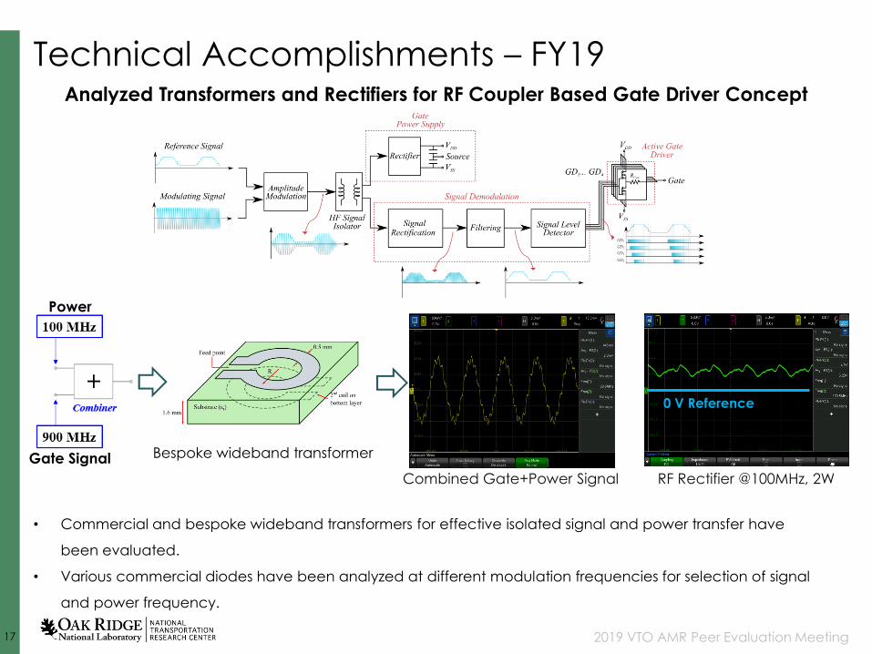
Technical Accomplishments – FY19Analyzed Transformers and Rectifiers for RF Coupler Based Gate Driver Concept
• Commercial and bespoke wideband transformers for effective isolated signal and power transfer have
been evaluated.
• Various commercial diodes have been analyzed at different modulation frequencies for selection of signal
and power frequency.
Bespoke wideband transformer
Power
Gate Signal
Combined Gate+Power Signal
0 V Reference
RF Rectifier @100MHz, 2W

1818 2019 VTO AMR Peer Evaluation Meeting
Responses to Previous Year Reviewers’ Comments
• This project is a new start

1919 2019 VTO AMR Peer Evaluation Meeting
Collaboration and Coordination with Other Institutions
Organization Role
Thermal Analysis of Substrates
WBG device models and samples
Quilt Packaging Interconnect Design and Manufacturing
IMS with TPG Insert Design and Manufacturing
Organic DBC Material Provider
2020 2019 VTO AMR Peer Evaluation Meeting
Remaining Challenges and Barriers for FY19
• Application of Quilt interconnects in vertical SiC power MOSFETs
• Impacts of parasitic components to the operation of the RF coupler
• Achieving high efficiency in RF coupler with harmonic content coming from
gate driver power supply

2121 2019 VTO AMR Peer Evaluation Meeting
Proposed Future Work
Any proposed future work is subject to change based on funding levels
• Remainder of FY19– Experimental characterization of DBC, IMS and IMSwTPG substrates:
• Validate thermal performance
• Characterize dielectric breakdown characterization will be conducted
– Analyze of ODBC from DuPont and design the substrate for 100kW power module with different WBG devices
– Compare high power silicon carbide (SiC) MOSFET and gallium nitride (GaN) high electron mobility transistor (HEMT)
– Analyze electrical performance of quilt nodules for high power applications
• FY20– Build and evaluate high power WBG module for DOE ELT 2025 target system
– Design and test quilt based WBG power devices
– Experimentally validate RF based gate driver in a high power electronic inverter
Control and Power Board Design for Substrate Evaluation

2222 2019 VTO AMR Peer Evaluation Meeting
Summary
• Relevance: DOE ELT 2025 high voltage power electronics targets require revisiting the conventional silicon oriented integration to enable the benefits of WBG devices, and to achieve power density, cost and reliability targets
• Approach: Develop substrate, interconnect technologies for power modules, and high power density gate drivers to achieve high power density and reliability in next generation advanced integrated power electronic systems
• Collaborations: NREL, SNL, Momentive, Henkel, Indiana IC, and DuPont
• Technical Accomplishments: – Developed high performance IMS substrates with and without TPG insert, and completed
FEA based thermal comparison with SOA DBC– Conducted power cycling simulations with various substrates and evaluated performance
of each technology under different power cycling conditions– Designed various quilt interconnect based silicon chips for electrical evaluation of the
technology with different nodule size, thickness and testing conditions– Evaluated different transformer and modulation techniques for high performance RF
based gate driver solution
• Future Work:– Characterize different substrates in an experimental setup with SiC MOSFETs– Characterize quilt nodules under different current and temperature conditions– Build and evaluate RF based gate driver with optimum transformer and modulation
scheme– Develop substrate for 100kW inverter based on ODBC.
Any proposed future work is subject to change based on funding levels