highly passivating and blister-free hole selective poly
TRANSCRIPT

HAL Id: hal-02308383https://hal-centralesupelec.archives-ouvertes.fr/hal-02308383
Submitted on 19 Mar 2020
HAL is a multi-disciplinary open accessarchive for the deposit and dissemination of sci-entific research documents, whether they are pub-lished or not. The documents may come fromteaching and research institutions in France orabroad, or from public or private research centers.
L’archive ouverte pluridisciplinaire HAL, estdestinée au dépôt et à la diffusion de documentsscientifiques de niveau recherche, publiés ou non,émanant des établissements d’enseignement et derecherche français ou étrangers, des laboratoirespublics ou privés.
Highly passivating and blister-free hole selectivepoly-silicon based contact for large area crystalline
silicon solar cellsAudrey Morisset, Raphaël Cabal, Bernadette Grange, Clément Marchat, JoséAlvarez, Marie-Estelle Gueunier-Farret, Sébastien Dubois, Jean-Paul Kleider
To cite this version:Audrey Morisset, Raphaël Cabal, Bernadette Grange, Clément Marchat, José Alvarez, et al..Highly passivating and blister-free hole selective poly-silicon based contact for large area crys-talline silicon solar cells. Solar Energy Materials and Solar Cells, Elsevier, 2019, 200, pp.109912.10.1016/j.solmat.2019.109912. hal-02308383

Highly Passivating and Blister-free Hole Selective Poly-Silicon Based
Contact for Large Area Crystalline Silicon Solar Cells
Audrey Morisseta,b,c,*, Raphaël Cabala, Bernadette Grangea, Clément Marchatc, José Alvarezb,c,
Marie-Estelle Gueunier-Farretb, Sébastien Duboisa and Jean-Paul Kleiderb,c
aUniv. Grenoble Alpes, INES, F-73375 Le Bourget du Lac, France ; CEA, LITEN, Département des
Technologies Solaires, F-73375 Le Bourget du Lac, France.
bLaboratoire de Génie Electrique et Electronique de Paris, CNRS UMR 8507, CentraleSupelec, Univ.
Paris-Sud, Sorbonne Universités-UPMC Univ. Paris 06, F-91192 Gif-sur-Yvette Cedex, France.
cInstitut Photovoltaïque d’Ile-de-France (IPVF), 30 RD 128, 91120 Palaiseau, France.
*Corresponding author.
E-mail address: [email protected] (A. Morisset)
Highlights:
• Blister-free boron-doped poly-Si layers are obtained by PECVD through optimization of the
deposition temperature and gas ratio.
• The process developed is approaching the industrial standards (large area KOH-polished
wafers, SiOx growth included in standard RCA cleaning, semi-industrial PECVD tool).
• High and homogeneous surface passivation properties are obtained (iVoc = 734 mV and
J0 = 7 fA∙cm-2).
• Conductive spots detected by C-AFM are not mirroring pinholes within the interfacial SiOx
layer.

Abstract
Passivating the contacts of crystalline silicon (c-Si) solar cells with a poly-crystalline silicon (poly-Si)
layer on top of a thin silicon oxide (SiOx) is currently sparking interest for reducing recombination at
the interface between the metal electrode and the c-Si substrate. Hole-selective poly-Si/SiOx structures
could be particularly relevant to passivate the rear side of mass-produced p-type c-Si solar cells (i.e.,
PERC solar cells). In this study, we elaborate on the optimization of a hole-selective passivating
structure consisting of a boron-doped poly-Si layer on top of a chemically grown thin SiOx. The
poly-Si layer is prepared by Plasma Enhanced Chemical Vapor Deposition, which enables single-side
deposition. However, if not optimized, this deposition technique leads to degradation of the poly-Si
layer through a “blistering” phenomenon due to high hydrogen incorporation in the layer. To tackle
this, a study of the interplay between process parameters and blistering is undertaken in order to obtain
highly passivating and blister-free poly-Si/SiOx structures. By addition of a hydrogenation step, the
implied open circuit voltage (iVoc) provided by the structure is further improved, leading to a
maximum value of 734 mV demonstrated on symmetrical samples made from large area wafers. We
also conduct a Conductive-Atomic Force Microscopy (C-AFM) study with the aim of investigating the
pinholes formation in the SiOx interfacial layer that could explain the transport of free charge carriers
within the poly-Si/SiOx structure. We show that the current levels detected by C-AFM are affected by
an oxide layer that grows at the poly-Si top surface. We also demonstrate that conductive spots
detected by C-AFM are not likely to mirror conductive pinholes within the SiOx layer but are rather
linked to the poly-Si layer.
Keywords
Crystalline silicon, solar cells, passivating contacts, poly-silicon, PECVD, C-AFM

1. Introduction
Industrial homojunction crystalline silicon (c-Si) solar cells reach conversion efficiencies above
21%[1]. However, to collect photo-generated charge carriers these cell structures involve localized and
direct interfaces between the c-Si substrate and the metal electrodes. These interfaces are highly
defective and induce photo-voltage losses because of charge carrier recombination. Moreover, for
PERC solar cell structures, a lateral transport of charge carriers is needed to reach the localized metal
contacts which affects the cell series resistance[2]. A way to overcome these issues is to implement a
full area “passivating” contact, which consists of a highly-doped layer to ensure a good contact
selectivity on top of a thin buffer layer for chemical surface passivation of the c-Si substrate. A first
version of passivating contacts consisting of a highly-doped amorphous silicon (a-Si) layer on top of a
thin intrinsic a-Si layer was implemented in the a-Si/c-Si heterojunction solar cell structure and
enabled to reach conversion efficiency of 25.1% on a large area two-side contacted structure[3].
However, due to the presence of a-Si layers, the process temperature of heterojunction solar cells must
remain below 250°C which prevents temperature-activated phenomena (as gettering of impurities or
hydrogenation effects) to occur during the process, leading to the need for high quality c-Si wafers[4].
A promising way to passivate contacts while ensuring high-temperature stability is to use a
highly-doped polycrystalline silicon (poly-Si) layer on top of a thin silicon oxide (SiOx) layer. The
SiOx layer growth (thermal or chemical) is followed by the deposition of a-Si or poly-Si layers either
by Low-Pressure Chemical Vapor Deposition (LPCVD)[5–7], or by Plasma-Enhanced CVD
(PECVD)[8–13]. Recently, the fabrication of poly-Si layers using Physical Vapor Deposition (PVD)
was also demonstrated[14]. A consequent annealing step is performed to crystallize the deposited layer
and/or activate dopants. Doping of the poly-Si layer can be performed in-situ by addition of a dopant-
rich precursor gas (e.g. B2H6 or PH3)[8,11–13] or ex-situ (e.g. by diffusion[5,7] or ion
implantation[15,16]). An additional hydrogenation process is generally performed to further enhance
the surface passivation properties[11,12,17]. Poly-Si/SiOx passivating structures demonstrated
promising performances when integrated in solar cell devices with conversion efficiencies ≥ 25.8%
obtained on small area devices (~2×2 cm2)[18,19]. Conversion efficiencies ≥ 21.3% were also

achieved on a large area device (~156×156 mm2) with screen-printed metallization[7,13]. Despite the
promising performances, these are some remaining challenges:
• The integration of hole-selective poly-Si/SiOx structures at the rear surface of existing mass
produced p-type c-Si solar cells (i.e, PERC) could be one of the next significant evolutionary
steps of the photovoltaic industry. So far, hole-selective poly-Si/SiOx structures have been
mainly formed with boron-doped poly-Si layer (poly-Si(B)) and have historically demonstrated
lower passivation performances compared to their phosphorus counterparts[17]. Despite recent
progress achieved with poly-Si(B)/SiOx passivating structures on both planar and textured
surfaces[20–22], boron (B) is suspected to cause more defects in the structure, especially at the
interface with the SiOx layer[23], due to low B diffusivity in SiOx leading to B atoms piling-up
at the SiOx layer[24,25].
• The use of PECVD is interesting for single-side deposition of the poly-Si layer, but also for
optimizing the properties of the layer, notably by adding alloying elements like carbon or
oxygen[12,26]. However, due to the H-rich precursor gases, the deposited a-Si:H layer is likely
to blister, resulting in a severe degradation of the poly-Si layer after annealing[10,11]. Solving
the blistering issue requires a fine tuning of the deposition conditions (especially the deposition
temperature and the gas ratio)[10–12].
• The transport mechanism of charge carriers through the poly-Si/SiOx structure has recently
been actively investigated but is still not fully understood yet[27–31]. Two hypothetical
transport regimes have been identified: a regime of charge carriers tunneling through the SiOx
layer[32], and a regime of direct transport through pinholes formed in the SiOx layer upon
annealing[33]. The poly-Si/SiOx structure was notably studied by means of Conductive-Atomic
Force Microscopy (C-AFM) with the aim of detecting pinholes in the SiOx layer[34,35].
This contribution focuses on poly-Si(B)/SiOx structures prepared by PECVD with the aim of
integrating the structure at the rear side of a p-type c-Si solar cell (see Fig. 1). First, we address the
optimization of the deposition temperature and gas ratio that enabled to obtain blister-free
poly-Si(B)/SiOx structures while insuring good surface passivation properties. Surface passivation
properties were improved by optimizing the annealing temperature and by addition of a post-process

hydrogenation step. Then, Conductive-Atomic Force Microscopy (C-AFM) measurements were
performed to investigate the formation of conductive pinholes in the SiOx layer. We first evaluated the
impact of an oxide present at the poly-Si top surface on the current levels detected by C-AFM. We
then investigated the possible link between conductive spots observed on C-AFM current maps and
conductive pinholes in the SiOx layer.
Fig. 1. Schematic of a p-type c-Si solar cell where the (p+) poly-Si(B)/SiOx structure discussed in this paper is
integrated at the rear surface. The cell features a front (n+) c-Si emitter that is coated with an anti-reflective
hydrogen-rich silicon nitride layer (SiN:H). Local Ag metal contacts are formed on the front side. The rear
contact consists of a full-area metal layer (e.g. Ag, Al).
2. Experimental
2.1. Sample preparation
In order to optimize the deposition parameters, single side poly-Si(B) passivating structures were
fabricated using 275 μm-thick double-side-mirror-polished 4 inch n-type Czochralski (Cz) (100) c-Si
wafers (resistivity (ρ) of 2-3 Ω∙cm). A thin SiOx layer (~1.3 nm) was grown on the wafers surface by
integrating a 10 min-long ozonized DI-H2O rinsing in our wet chemical cleaning. A hydrogen-rich
boron-doped a-Si layer (a-Si:H(B)) was single-side deposited by PECVD on top of the SiOx layer,
using a 13.56 MHz PECVD reactor. Precursor gases consisted of silane (SiH4), hydrogen (H2), and H2-
diluted diborane (B2H6). The a-Si:H(B) layer thickness was targeted in the range 20-30 nm. The
samples were annealed in the range 700-900°C in a tube furnace under argon atmosphere in order to
Metal
(n+) c-Si
(p) c-Si
(p+) poly-Si
SiOx
SiN:HAg Ag

activate dopants and crystallize the a-Si:H(B) layer. Samples were loaded at 400°C with a ramp rate of
~10°C/min to reach the annealing temperature (Ta) for a 30 min plateau and were unloaded at 700°C
with a similar ramp rate down (for Ta > 700°C). In the following, we use the term “poly-Si” to refer to
the layer after annealing. For the C-AFM study, samples “without interfacial SiOx” were prepared the
same way except that the c-Si wafer was dipped in hydrofluoric acid (HF) prior to the PECVD step
(delay < 5 min) in order to remove the interfacial SiOx layer, leading to a poly-Si(B)/c-Si stack.
The effect of the poly-Si annealing temperature and hydrogenation on surface passivation
properties was evaluated on symmetrical samples made from the afore-described mirror-polished
4 inch c-Si wafers and also from 180 μm-thick KOH-polished 156 mm pseudo square (psq) n-type Cz
(100) wafers (ρ = 6 Ω∙cm). The process was similar to the one previously described except that the
a-Si:H(B) layer was deposited by PECVD on both sides of the wafer. The annealing step was followed
by a hydrogenation step consisting of the deposition of H-rich silicon nitride layer on top of the poly-
Si layer followed by a firing step in a conventional belt furnace (Tfiring ~ 760°C). A subsequent
chemical etching of the SiN:H layer was performed on these samples by dipping them in a
concentrated HF solution for approximately 1 min.
2.2. Characterization techniques
The thickness of SiOx, a-Si:H(B) and final poly-Si(B) layers was measured by spectroscopic
ellypsometry (SE) (Jobin Yvon tool, HORIBA) on mirror-polished c-Si wafers. For the fitting model
of the poly-Si(B) layer, we considered a layer consisting of a mix of crystalline clusters in an
amorphous matrix (adapted from ref.[36]). The thickness of the layer measured by SE after deposition
and after annealing were in good agreement with the targeted thickness (within ±2 nm of error) so to
simplify the following, only the targeted thickness will be mentioned. The imaginary part of the
dielectric function obtained as a function of the photon energy through SE measurement was used to
verify the amorphous nature of a-Si:H(B) layers after deposition (curve featuring a broad peak
centered around 3.3 eV) and the crystallization of the poly-Si layer after annealing (curve featuring
two peaks centered around 3.4 and 4.2 eV)[36].

Optical microscopic observations of the poly-Si(B) layer after annealing were performed with a
BX61 tool (Olympus). The resulting images were analyzed using the software ImageJ to assess the
blister diameter and density.
Electrical properties (conductivity, Hall mobility and charge carrier concentration) of the poly-
Si(B) layer were evaluated by Hall effect technique (HMS-5500 tool, Ecopia) on laser cut 2×2 cm2
pieces of samples. Electrochemical capacitance-voltage (ECV) measurements were carried out to
estimate the majority carrier (approximated as the active boron) concentration profile in the poly-Si(B)
layer using a ECV WEP CVP21 tool with a 0.1 mol/l NH4F solution as etchant.
The effective carrier lifetime was measured by photo-conductance decay (PCD) technique using a
WCT 120 tool (Sinton Instruments), in order to obtain the implied open circuit voltage (iVoc) and the
recombination current density (J0) (extracted using the method of Kane and Swanson[37]). The surface
passivation properties provided by the poly-Si(B)/SiOx structure were evaluated on symmetrical
samples fabricated from mirror-polished 4 inch c-Si wafers and from 156 psq KOH-polished c-Si
wafers. On the latter, we performed a five-point mapping of the PCD measurement (one measurement
in the center and four measurements at approximately 4 cm of the edges) to evaluate the spatial
homogeneity of surface passivation properties after annealing. The PCD measurement was also
performed after SiN:H chemical etching.
Conductive atomic force microscopy (C-AFM) measurements were carried out with an AFM
Combiscope AIST-NT (HORIBA) with an integrated Resiscope module on samples made from
mirror-polished c-Si wafers. C-AFM measurements were conducted in contact mode using PtSi-FM
tips (Nanosensors) placed at the poly-Si(B) surface, under air and dark conditions. A polarization of -1
V was applied between the tip and the second contact. C-AFM measurements were performed in two
different configurations:
• In transversal configuration i.e. the voltage was applied between the AFM tip and a silver
contact located at the back side of the c-Si.
• In lateral configuration i.e. the voltage was applied between the AFM tip and a silver contact
localized at the poly-Si(B) surface (resulting in a short-circuit of the layer).

The resulting current maps were analyzed using the software ImageJ to assess the density of
conductive spots.
3. Results and discussion
3.1. Optimization of the poly-Si(B)/SiOx structure
3.1.1 Blistering reduction
Several studies have shown that poly-Si/SiOx structures fabricated by PECVD of a-Si:H layer on
top of SiOx are prone to blistering[10–12]. The blistering phenomenon is observed during the
deposition of the a-Si:H layer and also during the annealing step to form poly-Si. Even though a
fundamental understanding of the phenomenon is still lacking, some hypotheses have been proposed.
Blistering during PECVD might be related to adhesion properties of the a-Si:H film to the SiOx layer
coupled with a high amount of H incorporated in the layer, leading to the accumulation of H2
molecules at the a-Si:H(B)/SiOx interface[38]. Blistering during the annealing step is likely due to
rapid release of H2 at high temperature[39]. As a consequence, a severe degradation of the final
poly-Si(B) layer is observed if the deposition and annealing conditions are not optimized[10,11].
In this part we address the optimization of the PECVD parameters in order to minimize the
incorporation of H in the a-Si:H(B) layer, reducing therefore blistering of the final poly-Si(B) layer. In
all the work presented here, the annealing step was performed by placing the samples in the furnace at
low temperature (400°C) followed by a slow ramp-up rate (~10°C/min) to reach the targeted annealing
temperature (Ta) in order to mitigate blistering during annealing. As a first step, 30 nm-thick a-Si:H(B)
layers were deposited on top of SiOx using a deposition temperature Tdep = 220°C and a gas ratio
R = H2/SiH4 = 6 which resulted in a severe blistering of the layer after both deposition and annealing at
Ta = 700°C (see Fig. 2). The first way to minimize the incorporation of H in the a-Si:H(B) layer was to
increase the deposition temperature (Tdep) leading to the reduction of H incorporation in the deposited
layer[39,40]. In this study, the increase of Tdep from 220°C to 300°C (limit of the PECVD equipment)
enabled to reduce the blister diameter from 20 μm to 8 μm after deposition and from 30 μm to 13 μm
after annealing (Fig. 2, Step 1), however, the blister density remained unchanged (1.5 mm-2).

Fig. 2. Optical microscope images of 30 nm-thick poly-Si(B) layers after deposition and after annealing at 700°C
(at a ×20 magnification). The deposition conditions were varied: Step 1. Increase of the deposition temperature
Tdep, Step 2. Increase of the gas flow ratio R = H2/SiH4. For each set of conditions, the diameter of the blisters (Ø
blisters) and their density were evaluated.
The second way to reduce the blistering was to increase the gas flow ratio R = H2/SiH4 during the
deposition step[11]. It is to note that high R during the PECVD step could lead to microcrystalline
deposited layers, however, as the deposited layer was in-situ doped with B, it remained amorphous
(which was verified by spectroscopic ellipsometry (SE))[41]. The increase of R led to a reduction of
the blister density after deposition and after annealing from 1.5 mm-2 to 0.6 mm-2 for R from 6 to 50
respectively (Fig. 2, Step 2). Increasing R to 65 enabled to obtain blister-free poly-Si(B) layers. Fig. 3a
depicts the deposition rate as a function of the gas ratio R. Increasing R led to the decrease of the
deposition rate which is assumed to promote H atoms diffusion toward the top surface of the layer
during the deposition step, thus mitigating the blistering phenomenon. Fig. 3a also depicts the iVoc
(assessed on mirror-polished samples) as a function of the gas ratio R. For R = 25 to R = 50, an
increase of iVoc of 90 mV was observed, concomitantly to blistering reduction. When further
increasing R to 65, a drop of 20 mV in iVoc was observed. This drop was attributed to the excessive H2
concentration in the plasma causing radiation induced charges in the SiOx layer[42,43]. An optimal gas
ratio of R = 50 was found to reduce the blister density (0.6 mm-2 for a poly-Si thickness of 30 nm) and
preserve decent iVoc after annealing at 700°C. The remaining blistering was avoided by decreasing the
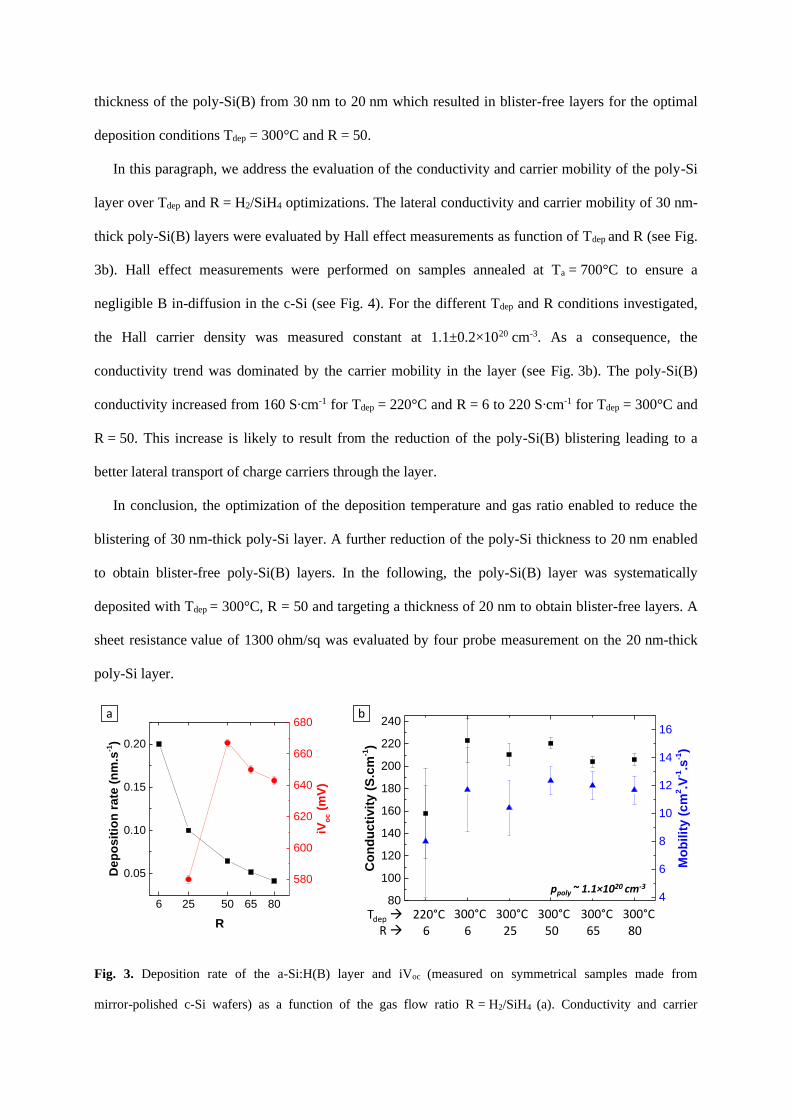
thickness of the poly-Si(B) from 30 nm to 20 nm which resulted in blister-free layers for the optimal
deposition conditions Tdep = 300°C and R = 50.
In this paragraph, we address the evaluation of the conductivity and carrier mobility of the poly-Si
layer over Tdep and R = H2/SiH4 optimizations. The lateral conductivity and carrier mobility of 30 nm-
thick poly-Si(B) layers were evaluated by Hall effect measurements as function of Tdep and R (see Fig.
3b). Hall effect measurements were performed on samples annealed at Ta = 700°C to ensure a
negligible B in-diffusion in the c-Si (see Fig. 4). For the different Tdep and R conditions investigated,
the Hall carrier density was measured constant at 1.1±0.2×1020 cm-3. As a consequence, the
conductivity trend was dominated by the carrier mobility in the layer (see Fig. 3b). The poly-Si(B)
conductivity increased from 160 S∙cm-1 for Tdep = 220°C and R = 6 to 220 S∙cm-1 for Tdep = 300°C and
R = 50. This increase is likely to result from the reduction of the poly-Si(B) blistering leading to a
better lateral transport of charge carriers through the layer.
In conclusion, the optimization of the deposition temperature and gas ratio enabled to reduce the
blistering of 30 nm-thick poly-Si layer. A further reduction of the poly-Si thickness to 20 nm enabled
to obtain blister-free poly-Si(B) layers. In the following, the poly-Si(B) layer was systematically
deposited with Tdep = 300°C, R = 50 and targeting a thickness of 20 nm to obtain blister-free layers. A
sheet resistance value of 1300 ohm/sq was evaluated by four probe measurement on the 20 nm-thick
poly-Si layer.
Fig. 3. Deposition rate of the a-Si:H(B) layer and iVoc (measured on symmetrical samples made from
mirror-polished c-Si wafers) as a function of the gas flow ratio R = H2/SiH4 (a). Conductivity and carrier
6 25 50 65 80
0.05
0.10
0.15
0.20
R
Dep
osit
ion
rate
(n
m.s
-1)
580
600
620
640
660
680
iVo
c (
mV
)
80
100
120
140
160
180
200
220
240
Co
nd
ucti
vit
y (
S.c
m-1)
4
6
8
10
12
14
16
Mo
bilit
y (
cm
2.V
-1.s
-1)
220°C 300°C6 6 25 50 65 80
Tdep →
R →
ppoly ~ 1.1×1020 cm-3
300°C 300°C 300°C 300°C
ba

mobility of 30 nm-thick poly-Si(B) layers measured by Hall effect technique as function of the deposition
temperature (Tdep) and gas ratio (R) optimizations (b). Samples were annealed at Ta = 700°C. The carrier density
of poly-Si(B) layers (ppoly) was evaluated by Hall effect measurement and was constant with an average value of
1.1±0.2×1020 cm-3.
3.1.2 Impact of annealing temperature on surface passivation properties
In this part we address the impact of the annealing temperature (Ta) on the resulting poly-
Si(B)/SiOx surface passivation properties. Several studies evidenced an optimal Ta to maximize the
surface passivation provided by the poly-Si(B)/SiOx structure. This optimum corresponds to a trade-
off between two T-activated phenomena:
• The shallow in-diffusion of dopants from the poly-Si layer to the c-Si substrate, which
enhances the field-effect passivation at the c-Si surface[44,45]
• The degradation of the interfacial SiOx layer which decreases the chemical passivation
properties (interface state density (Dit) increase)[17,46,47]
The poly-Si(B)/SiOx samples were first fabricated on mirror polished c-Si wafers. The a-Si:H(B)
layer was deposited with optimized deposition conditions (Tdep = 300°C and R = 50). Samples were
then annealed at Ta = 700°C, 800°C or 900°C. The crystalline nature of the poly-Si layer after
annealing was verified by SE. A poly-Si(B) thickness of 20 nm was targeted, resulting in blister-free
layers after annealing. For each Ta, the active B concentration profile of the poly-Si(B) layer was
measured by ECV, the resulting profiles are depicted in Fig. 4.
For Ta = 700°C, the Hall effect measurement resulted in a Hall carrier density of 1.3±0.2×1020 cm-3.
From the B concentration profile obtained by ECV in the poly-Si(B) layer, a carrier density of
1.7±0.1×1020 cm-3 was evaluated which is in good agreement with the Hall carrier density. The
increase of Ta to 800°C and 900°C resulted in a significant B in-diffusion in the c-Si substrate (30 nm
and 160 nm-deep, respectively). As a consequence, the evaluation of the poly-Si(B) electrical
properties via Hall effect measurement was not possible due to the current flowing in the p+-doped part
of the c-Si.

For each Ta, surface passivation properties were evaluated, the resulting iVoc values are indicated in
Fig. 4, with their associated B concentration profiles. An optimal Ta of 800°C was found to maximize
the iVoc value to 690 mV and minimize the J0 value to 30 fA/cm2. When increasing Ta up to 900°C a
decrease of iVoc to 630 mV was observed as well as an increase of J0 to 260 fA/cm2, attributed to the
combination of the deep B in-diffusion in the c-Si and the degradation of the SiOx interfacial layer.
Fig. 4. Hole concentration (approximated as the active boron) profiles measured by electrochemical
capacitance-voltage (ECV) on samples annealed at different temperatures (Ta).
Using the same deposition conditions we studied the impact of Ta on surface passivation of 156 psq
KOH-polished c-Si wafers, which corresponds to the area and topography targeted for device
integration of the poly-Si(B)/SiOx passivating structure. Fig. 5 depicts the average iVoc and J0 values
measured after annealing as function of Ta in the range 700 – 850°C (on five samples per Ta value
investigated). A similar trend as in the case of mirror-polished samples was observed: from
Ta = 700°C to 800°C the iVoc value increased from 661 mV to 689 mV respectively. For Ta = 850°C,
the iVoc value dropped to 664 mV. An optimal Ta value of 800°C was found to maximize iVoc and
minimize J0 after annealing. The PCD technique was performed on 5 points per sample to evaluate the
spatial homogeneity of the surface passivation properties after annealing. A spatial dispersion of 3 mV
and 2.5 fA∙cm-2 was evaluated for iVoc and J0 respectively, showing the good homogeneity of the
poly-Si(B)/SiOx fabrication process on large area wafers.
0 30 60 90 120 150 180
1015
1016
1017
1018
1019
1020
Ho
le c
on
cen
trati
on
(cm
-3)
Etch depth (nm)
Ta = 700°C
Ta = 800°C
Ta = 900°C
iVoc = 660 mV
iVoc = 690 mV
iVoc = 630 mV

Fig. 5. Surface passivation properties (iVoc (a) and J0 (b)) provided by the poly-Si(B)/SiOx structure as function
of the annealing temperature Ta, evaluated on symmetrical samples (made from KOH-polished 156psq c-Si
wafers) after annealing, SiN:H deposition and firing (dpoly = 20 nm).
3.1.3 Impact of the hydrogenation step
The surface passivation properties provided by the poly-Si(B)/SiOx structure fabricated on
KOH-polished c-Si wafers were further improved by depositing a hydrogenated silicon nitride (SiN:H)
layer on top of the poly-Si(B) (both sides), followed by a firing step. The resulting iVoc and J0 values
measured after SiN:H deposition and after a subsequent firing step are plotted in Fig. 5. The SiN:H
deposition did not impact significantly the iVoc value over the entire Ta range although slightly
decreasing the J0 values. For every sample annealed at Ta ≤ 800°C, performing a subsequent firing step
resulted in an increase of iVoc above 700 mV as well as a decrease of J0 below 10 fA∙cm-2. A
maximum iVoc of 721 mV was reached for Ta = 750°C, corresponding to a J0 value of 5.3 fA∙cm-2.
After firing, one can note that the lower the Ta the greater the absolute gain in iVoc and J0.
By fabricating similar samples using better quality KOH-polished 156psq n-type Cz c-Si wafers, an
average iVoc of 731 mV was obtained after annealing at Ta = 700°C with a best value of 734 mV
(corresponding to a J0 of 7 fA∙cm-2). This is among the best values obtained so far with p+-poly-Si

symmetrical samples on planar surface (in the range 732-735 mV for iVoc and 1-10 fA∙cm-2 for
J0)[14,20,21,23]. Values of 720 mV and 10 fA∙cm-2 were also demonstrated on textured surface[22].
As mentioned in the introduction, we aim to integrate the poly-Si(B)/SiOx structure at the rear side
of a p-type solar cell with a full area rear metallization[14] (see Fig. 1), which implies the removal of
the SiN:H layer prior to metal deposition. After chemical etching of the SiN:H layer, the surface
passivation properties remained good on all the Ta range investigated (iVoc average loss < 4 mV).
3.2 Investigation of transport mechanisms within the interfacial oxide
The transport mechanism of charge carriers through the poly-Si/SiOx structure has recently been
actively investigated[27–31]. It has been found to be process dependent and two hypothetical transport
regimes have been identified: a regime of charge carriers tunneling through thin SiOx layer (< 2 nm)
exposed to moderate temperature annealing (Ta < 800°C)[32], and a regime of direct transport through
pinholes formed in the SiOx layer upon annealing, generally achieved by growing a thicker SiOx layer
(> 2 nm) and exposed to high temperature annealing (Ta > 1000°C)[33]. C-AFM measurements on
poly-Si/SiOx structures have been reported in the literature with the aim of detecting the presence of
pinholes in the SiOx layer[34,35]. Localized regions of higher current intensity (conductive spots)
were observed on the resulting C-AFM current maps. However, a clear link between these conductive
spots and the presence of pinholes within the SiOx layer has not been established yet.
In the present study, we first evaluated the impact of an oxide present at the poly-Si top surface on
the current levels detected by C-AFM. Then, we investigated the link between conductive spots
observed on C-AFM current maps and the presence of pinholes in the interfacial SiOx layer by
performing measurements in different configurations (transversal or lateral), with and without SiOx
layer at the poly-Si/c-Si interface.
3.2.1 Impact of the surface oxide on the C-AFM measurement
Despite the inert atmosphere imposed during the annealing step, an oxide layer of approximately
3 nm was measured by SE at the surface of our samples (i.e. at the poly-Si(B) top surface) probably
due to the tube furnace used during annealing which is not being sealed (no load lock). A preliminary
study consisted in evaluating the impact of this oxide on the current levels detected by C-AFM.
A first C-AFM measurement was performed in transversal configuration (i.e. the voltage was
applied between the AFM tip and a contact located at the back side of the c-Si) on a sample featuring a
20 nm-thick poly-Si(B) layer annealed at 700°C (deposited on n-type mirror-polished c-Si wafer). The
oxide at the poly-Si(B) top surface was then removed through a HF-cleaning step and followed by
several transversal C-AFM measurements performed from 30 min to 5h after HF-cleaning, the
samples being stored under air in the meantime. The resulting current maps measured after annealing
and at different times after HF-cleaning are depicted in Fig. 6. From the current maps, the surface
distribution of the detected current was extracted (Fig. 7). After annealing, the current distribution
curve features a peak at 3.9 pA corresponding to the mean current intensity (Imean) and a maximum
current intensity (Imax) detected at 5.8 nA. The C-AFM measurement performed 30 min after
HF-cleaning showed an increase of Imean and Imax up to 0.25 nA and 114.7 nA respectively. The C-AFM
measurement performed 2h after the HF-cleaning step showed then a decrease of Imean and Imax (down
to 4.9×10⁻² nA and 88.7 nA respectively) due to the re-growth of an oxide layer at the sample’s
surface. The measurement performed 5h after cleaning showed similar values of Imean and Imax than
after 2h, indicating that the surface oxide layer did not evolve significantly in between these two
measurements.
These results emphasized the impact of the oxide at the surface of the samples after annealing that
decreased the current levels detected by C-AFM. To avoid any misinterpretation due to a different
surface state, C-AFM measurements presented in the following part were performed with a constant
delay between the HF-cleaning and the measurement.

Fig. 6. Current maps obtained by C-AFM measurement in transversal configuration on a 20 nm-thick poly-Si(B)
layer annealed at 700°C (a) and at different times after HF-cleaning the poly-Si(B) surface (30 min (b) and 5h
(c)).
Fig. 7. Surface distribution of the detected currents extracted from C-AFM current maps measured at the
poly-Si(B) surface in transversal configuration after annealing at 700°C and at different times after HF-cleaning
the poly-Si(B) surface (from 30min to 5h).
3.2.2 C-AFM investigation of the pinholes formation within the SiOx layer

C-AFM measurements performed on poly-Si/SiOx structures result in the detection of localized
regions of higher current intensity (conductive spots). Moreover, Lancaster et al. detected higher
current levels when performing C-AFM on poly-Si/SiOx structures annealed at 950°C than on
structures annealed at 800°C[34]. They proposed that this observation could result from a lower
resistance of the SiOx layer as the density of pinholes in the SiOx layer has been observed to increase
with increasing Ta[48]. To investigate the possible link between these conductive spots and pinholes in
the interfacial SiOx layer, C-AFM measurements were performed on samples annealed at different
temperatures. 20 nm-thick poly-Si(B) layers were deposited with optimized conditions (Tdep = 300°C
and R = 50) on n-type mirror-polished c-Si wafers. The annealing temperature was varied in the range
700°C to 900°C. C-AFM measurements were performed with a constant delay of 2h after HF-cleaning
the samples’ surface. Fig. 8a and Fig. 8b depict current maps obtained in transversal configuration on
poly-Si layers annealed at 700°C and 900°C. The density of conductive spots (> 1 nA) was found to
increase from 55 μm-2 to 215.4 μm-2 respectively. The current levels were found to increase with
increasing Ta from 700°C to 900°C which is in good agreement with observations of Lancaster et
al.[34], and could result from a lower electrical resistance of the SiOx layer due to conductive pinholes
forming in the layer upon annealing at higher Ta. Moreover, the increase of the conductive spots
density with increasing Ta is consistent with the increase of pinhole density with increasing Ta[48] and
could lead to the hypothesis that the conductive spots detected by C-AFM are mirroring pinholes
within the interfacial SiOx layer.

Fig. 8. Current maps obtained by C-AFM measurement in transversal configuration at the surface of samples
with an intentionally grown SiOx layer at the poly-Si(B)/c-Si interface after annealing at 700°C (a) and at 900°C
(b). The same measurement was performed on a sample without interfacial SiOx layer (annealed at 700°C) (c).
C-AFM measurements were systematically performed 2h after HF-cleaning the samples’ surface to ensure a
similar surface state during the measurement.
To further investigate the correlation between conductive spots and pinholes in the SiOx layer, we
performed C-AFM measurements on a sample featuring a similar poly-Si(B) layer without interfacial
SiOx layer. This sample was fabricated by dipping the c-Si wafer in HF prior to the a-Si deposition
step in order to remove the interfacial SiOx layer, leading to a poly-Si/c-Si stack (Ta = 700°C). The C-
AFM measurement was performed 2h after HF-cleaning the sample’s surface. The pattern of the
resulting current map was similar to the one obtained in the case of an intentionally grown interfacial
SiOx layer (Fig. 8a), with a density of conductive spots in the same range (50.8 μm-2, Fig. 8c).

However, lower current levels were detected, although the resistance of the poly-Si/c-Si stack was
expected to be lower due to the absence of interfacial SiOx layer. The slightly lower current levels
obtained could result from a larger resistance of the poly-Si layer as the crystalline structure of the
poly-Si layer is expected to depend on the surface state of the c-Si wafer (oxidized or HF-cleaned)
before deposition. Despite the lower current levels, the detection of conductive spots when performing
C-AFM measurements on a sample without interfacial SiOx layer is disproving the hypothesis that
conductive spots could mirror pinholes in the SiOx layer.
To further investigate on the conductive spots observed on current maps, additional C-AFM
measurements were performed on similar samples in lateral configuration (i.e. the voltage was applied
between the AFM tip and a silver contact localized at the poly-Si(B) surface), with and without SiOx
layer at the poly-Si/c-Si interface (Ta = 700°C). C-AFM measurements were performed with a delay of
5h after HF-cleaning the samples’ surface. Resulting current maps are depicted in Fig. 9. The current
maps showed conductive spots (> 1 nA) with a density of 24.9 μm-2 and 11.2 μm-2 with and without
SiOx respectively. The current levels detected on the sample with interfacial SiOx (Fig. 9a) were
slightly higher than the ones detected without SiOx layer (Fig. 9b) which is consistent with the
transversal C-AFM measurements on similar samples (Fig. 8a and 8c respectively) and supports the
hypothesis that it is related to change in the conduction properties of the poly-Si layer. The lower
current levels and lower conductive spots densities detected in lateral configuration (Fig. 9) compared
to measurements in transversal configuration (Fig. 8) are resulting from the longer delay between the
samples HF-cleaning and the lateral measurements (measured 3h later). A qualitative comparison of
the lateral and transversal current maps is nevertheless possible. One can notice a similar current
pattern in both configurations although in lateral configuration, the current is expected to flow
principally in the poly-Si layer. These observations suggest that the conductive spots observed on C-
AFM current maps are linked to the poly-Si microstructure rather than mirroring pinholes in the SiOx
layer. Conductive spots could be the result of a different local conduction in the poly-Si layer, e.g. the
crystalline grains would conduct differently than the grain boundaries (or remaining amorphous
phases), as it was observed in ref. [49].

Fig. 9. Current maps obtained by C-AFM measurement in lateral configuration on 20 nm-thick poly-Si(B) layers
(Ta = 700°C) with (a) and without (b) SiOx layer at the poly-Si(B)/(n)c-Si interface. C-AFM measurements were
performed 5h after HF-cleaning the samples’ surface to ensure a similar surface state during both measurements.
4. Conclusion
In conclusion, we presented highly passivating and blister-free poly-Si(B)/SiOx structures
fabricated by PECVD with the aim of passivating c-Si solar cell contacts. First, the blistering issue
appearing because of the high H content of the a-Si:H deposited layer was overcome by optimizing the
deposition temperature and gas ratio. For poly-Si(B)/SiOx structures made on KOH-polished 156 psq
c-Si wafers, the surface passivation properties were further improved by addition of a hydrogenation
step leading to a maximum iVoc value of 734 mV.
The poly-Si(B)/SiOx samples were then studied by means of C-AFM with the aim of investigating
the formation of conductive pinholes in the SiOx layer. We showed that the growth of an oxide at the
poly-Si top surface affects the current levels detected by C-AFM. We observed similar C-AFM current
patterns in transversal configuration on samples with and without interfacial SiOx layer as well as in
lateral configuration where the current is expected to flow principally in the poly-Si layer. These
observations disprove the hypothesis that conductive spots detected by C-AFM would mirror pinholes
within the SiOx layer but rather suggest that the conductive spots would relate to the poly-Si
microstructure.

Funding
This work was supported by the French National Research Agency (Programs “Investment for the
Future” ANR-IEED-002-01, ANR-10-ITE-0003 and “Oxygen” ANR-17-CE05-0035) and has also
received funding from the European Union’s Horizon 2020 research and innovation program under
grant agreement No 727529.
References
[1] T. Dullweber, J. Schmidt, Industrial Silicon Solar Cells Applying the Passivated Emitter and
Rear Cell (PERC) Concept—A Review, IEEE J. Photovolt. 6 (2016) 1366–1381.
doi:10.1109/JPHOTOV.2016.2571627.
[2] S.W. Glunz, F. Feldmann, A. Richter, M. Bivour, C. Reichel, H. Steinkemper, J. Benick, M.
Hermle, The irresistible charm of a simple current flow pattern - 25% with a solar cell featuring
a full-area back contact, Proc. 31st Eur. Photovolt. Sol. Energy Conf. Exhib. (2015) Hamburg,
Germany.
[3] D. Adachi, J.L. Hernández, K. Yamamoto, Impact of carrier recombination on fill factor for
large area heterojunction crystalline silicon solar cell with 25.1% efficiency, Appl. Phys. Lett.
107 (2015) 233506. doi:10.1063/1.4937224.
[4] S. De Wolf, A. Descoeudres, Z.C. Holman, C. Ballif, High-efficiency Silicon Heterojunction
Solar Cells: A Review, Green. 2 (2012). doi:10.1515/green-2011-0018.
[5] U. Römer, R. Peibst, T. Ohrdes, B. Lim, J. Krügener, E. Bugiel, T. Wietler, R. Brendel,
Recombination behavior and contact resistance of n+ and p+ poly-crystalline Si/mono-
crystalline Si junctions, Sol. Energy Mater. Sol. Cells. 131 (2014) 85–91.
doi:10.1016/j.solmat.2014.06.003.
[6] F. Feldmann, C. Reichel, R. Müller, M. Hermle, The application of poly-Si/SiO x contacts as
passivated top/rear contacts in Si solar cells, Sol. Energy Mater. Sol. Cells. 159 (2017) 265–271.
doi:10.1016/j.solmat.2016.09.015.
[7] M.K. Stodolny, J. Anker, B. Geerligs, G.J.M. Janssen, B.W.H. van de Loo, J. Melskens, R.
Santbergen, O. Isabella, J. Schmitz, M. Lenes, J.-M. Luchies, W.M.M. Kessels, I. Romijn,
Material properties of LPCVD processed n-type polysilicon passivating contacts and its
application in PERPoly industrial bifacial solar cells, Energy Procedia. (2017) 635–642.
[8] F. Feldmann, M. Bivour, C. Reichel, M. Hermle, S.W. Glunz, Passivated rear contacts for high-
efficiency n-type Si solar cells providing high interface passivation quality and excellent
transport characteristics, Sol. Energy Mater. Sol. Cells. 120 (2014) 270–274.
doi:10.1016/j.solmat.2013.09.017.
[9] Y. Larionova, M. Turcu, S. Reiter, R. Brendel, D. Tetzlaff, J. Krügener, T. Wietler, U. Höhne,
J.-D. Kähler, R. Peibst, On the recombination behavior of p + -type polysilicon on oxide
junctions deposited by different methods on textured and planar surfaces: On the recombination
behavior of p + -type polysilicon on oxide junctions, Phys. Status Solidi A. 214 (2017) 1700058.
doi:10.1002/pssa.201700058.
[10] Y. Tao, V. Upadhyaya, Y.-Y. Huang, C.-W. Chen, K. Jones, A. Rohatgi, Carrier selective tunnel
oxide passivated contact enabling 21.4% efficient large-area n-type silicon solar cells, in:
Photovolt. Spec. Conf. PVSC 2016 IEEE 43rd, IEEE, 2016: pp. 2531–2535.
[11] B. Nemeth, D.L. Young, M.R. Page, V. LaSalvia, S. Johnston, R. Reedy, P. Stradins,
Polycrystalline silicon passivated tunneling contacts for high efficiency silicon solar cells, J.
Mater. Res. 31 (2016) 671–681. doi:10.1557/jmr.2016.77.
[12] G. Nogay, J. Stuckelberger, P. Wyss, E. Rucavado, C. Allebé, T. Koida, M. Morales-Masis, M.
Despeisse, F.-J. Haug, P. Löper, C. Ballif, Interplay of annealing temperature and doping in hole

selective rear contacts based on silicon-rich silicon-carbide thin films, Sol. Energy Mater. Sol.
Cells. 173 (2017) 18–24. doi:10.1016/j.solmat.2017.06.039.
[13] N. Nandakumar, J. Rodriguez, T. Kluge, T. Groβe, L. Fondop, P. Padhamnath, N. Balaji, M.
König, S. Duttagupta, Approaching 23% with large‐area monoPoly cells using screen‐printed
and fired rear passivating contacts fabricated by inline PECVD, Prog. Photovolt. Res. Appl.
(2018). doi:10.1002/pip.3097.
[14] D. Yan, A. Cuevas, S.P. Phang, Y. Wan, D. Macdonald, 23% efficient p-type crystalline silicon
solar cells with hole-selective passivating contacts based on physical vapor deposition of doped
silicon films, Appl. Phys. Lett. 113 (2018) 61603. doi:10.1063/1.5037610.
[15] U. Romer, R. Peibst, T. Ohrdes, B. Lim, J. Krugener, T. Wietler, R. Brendel, Ion Implantation
for Poly-Si Passivated Back-Junction Back-Contacted Solar Cells, IEEE J. Photovolt. 5 (2015)
507–514. doi:10.1109/JPHOTOV.2014.2382975.
[16] D.L. Young, W. Nemeth, V. LaSalvia, M.R. Page, S. Theingi, J. Aguiar, B.G. Lee, P. Stradins,
Low-cost plasma immersion ion implantation doping for Interdigitated back passivated contact
(IBPC) solar cells, Sol. Energy Mater. Sol. Cells. 158 (2016) 68–76.
doi:10.1016/j.solmat.2016.05.044.
[17] F. Feldmann, M. Simon, M. Bivour, C. Reichel, M. Hermle, S.W. Glunz, Efficient carrier-
selective p- and n-contacts for Si solar cells, Sol. Energy Mater. Sol. Cells. 131 (2014) 100–104.
doi:10.1016/j.solmat.2014.05.039.
[18] A. Richter, J. Benick, F. Feldmann, A. Fell, M. Hermle, S.W. Glunz, n-Type Si solar cells with
passivating electron contact: Identifying sources for efficiency limitations by wafer thickness
and resistivity variation, Sol. Energy Mater. Sol. Cells. 173 (2017) 96–105.
doi:10.1016/j.solmat.2017.05.042.
[19] F. Haase, C. Klamt, S. Schäfer, A. Merkle, M. Rienäcker, J. Krügener, R. Brendel, R. Peibst,
Laser contact openings for local poly-Si-metal contacts, Silicon PV 2018. (2018) Lausanne,
Switzerland.
[20] G. Nogay, A. Ingenito, E. Rucavado, Q. Jeangros, J. Stuckelberger, P. Wyss, M. Morales-Masis,
F.-J. Haug, P. Loper, C. Ballif, Crystalline Silicon Solar Cells With Coannealed Electron- and
Hole-Selective SiC $_\textx$ Passivating Contacts, IEEE J. Photovolt. (2018) 1–8.
doi:10.1109/JPHOTOV.2018.2866189.
[21] S. Mack, J. Schube, T. Fellmeth, F. Feldmann, M. Lenes, J.-M. Luchies, Metallisation of Boron-
Doped Polysilicon Layers by Screen Printed Silver Pastes, Phys. Status Solidi RRL - Rapid Res.
Lett. 11 (2017) 1700334. doi:10.1002/pssr.201700334.
[22] A. Mewe, M. Stodolny, J. Anker, M. Lenes, X. Pagès, Y. Wu, K. Tool, B. Geerligs, I. Romijn,
Full wafer size IBC cell with polysilicon passivating contacts, in: Lausanne, Switzerland, 2018:
p. 40014. doi:10.1063/1.5049277.
[23] D.L. Young, B.G. Lee, D. Fogel, W. Nemeth, V. LaSalvia, S. Theingi, M. Page, M. Young, C.
Perkins, P. Stradins, Gallium-Doped Poly-Si:Ga/SiO2 Passivated Emitters to n-Cz Wafers With
iV oc >730 mV, IEEE J. Photovolt. 7 (2017) 1640–1645. doi:10.1109/JPHOTOV.2017.2748422.
[24] T. Yamamoto, K. ’ichi Uwasawa, T. Mogami, Bias temperature instability in scaled
p/sup+/polysilicon gate p-MOSFET’s, IEEE Trans. Electron Devices. 46 (1999) 921–926.
[25] R.B. Fair, Physical models of boron diffusion in ultrathin gate oxides, J. Electrochem. Soc. 144
(1997) 708–717.
[26] I. Mack, J. Stuckelberger, P. Wyss, G. Nogay, Q. Jeangros, J. Horzel, C. Allebé, M. Despeisse,
F.-J. Haug, A. Ingenito, P. Löper, C. Ballif, Properties of mixed phase silicon-oxide-based
passivating contacts for silicon solar cells, Sol. Energy Mater. Sol. Cells. 181 (2018) 9–14.
doi:10.1016/j.solmat.2017.12.030.
[27] F. Feldmann, G. Nogay, P. Löper, D.L. Young, B.G. Lee, P. Stradins, M. Hermle, S.W. Glunz,
Charge carrier transport mechanisms of passivating contacts studied by temperature-dependent J-
V measurements, Sol. Energy Mater. Sol. Cells. 178 (2018) 15–19.
doi:10.1016/j.solmat.2018.01.008.
[28] N. Folchert, M. Rienäcker, A.A. Yeo, B. Min, R. Peibst, R. Brendel, Temperature-dependent
contact resistance of carrier selective Poly-Si on oxide junctions, Sol. Energy Mater. Sol. Cells.
185 (2018) 425–430. doi:10.1016/j.solmat.2018.05.046.

[29] F. Feldmann, G. Nogay, J.-I. Polzin, B. Steinhauser, A. Richter, A. Fell, C. Schmiga, M. Hermle,
S.W. Glunz, A Study on the Charge Carrier Transport of Passivating Contacts, IEEE J.
Photovolt. (2018) 1–7. doi:10.1109/JPHOTOV.2018.2870735.
[30] S.W. Glunz, F. Feldmann, SiO2 surface passivation layers – a key technology for silicon solar
cells, Sol. Energy Mater. Sol. Cells. 185 (2018) 260–269. doi:10.1016/j.solmat.2018.04.029.
[31] A.S. Kale, W. Nemeth, H. Guthrey, E. Kennedy, A.G. Norman, M. Page, M. Al-Jassim, D.L.
Young, S. Agarwal, P. Stradins, Understanding the charge transport mechanisms through
ultrathin SiO x layers in passivated contacts for high-efficiency silicon solar cells, Appl. Phys.
Lett. 114 (2019) 83902. doi:10.1063/1.5081832.
[32] H. Steinkemper, F. Feldmann, M. Bivour, M. Hermle, Numerical Simulation of Carrier-Selective
Electron Contacts Featuring Tunnel Oxides, IEEE J. Photovolt. 5 (2015) 1348–1356.
doi:10.1109/JPHOTOV.2015.2455346.
[33] R. Peibst, U. Römer, Y. Larionova, M. Rienäcker, A. Merkle, N. Folchert, S. Reiter, M. Turcu,
B. Min, J. Krügener, D. Tetzlaff, E. Bugiel, T. Wietler, R. Brendel, Working principle of carrier
selective poly-Si/c-Si junctions: Is tunnelling the whole story?, Sol. Energy Mater. Sol. Cells.
158 (2016) 60–67. doi:10.1016/j.solmat.2016.05.045.
[34] K. Lancaster, S. Großer, F. Feldmann, V. Naumann, C. Hagendorf, Study of Pinhole
Conductivity at Passivated Carrier-selected Contacts of Silicon Solar Cells, Energy Procedia. 92
(2016) 116–121. doi:10.1016/j.egypro.2016.07.040.
[35] Z. Zhang, Y. Zeng, C.-S. Jiang, Y. Huang, M. Liao, H. Tong, M. Al-Jassim, P. Gao, C. Shou, X.
Zhou, B. Yan, J. Ye, Carrier transport through the ultrathin silicon-oxide layer in tunnel oxide
passivated contact (TOPCon) c-Si solar cells, Sol. Energy Mater. Sol. Cells. 187 (2018) 113–
122. doi:10.1016/j.solmat.2018.07.025.
[36] G.E. Jellison, M.F. Chisholm, S.M. Gorbatkin, Optical functions of chemical vapor deposited
thin‐film silicon determined by spectroscopic ellipsometry, Appl. Phys. Lett. 62 (1993) 3348–
3350. doi:10.1063/1.109067.
[37] D.E. Kane, R.M. Swanson, Measurement of the emitter saturation current by a contactless
photoconductivity decay method (silicon solar cells), Conf. Rec. IEEE Photovolt. Spec. Conf.
(1985) 578–583.
[38] J.A. Aguiar, D. Young, B. Lee, W. Nemeth, S. Harvey, T. Aoki, M. Al-Jassim, P. Stradins,
Atomic scale understanding of poly-Si/SiO 2/c-Si passivated contacts: Passivation degradation
due to metallization, in: Photovolt. Spec. Conf. PVSC 2016 IEEE 43rd, IEEE, 2016: pp. 3667–
3670.
[39] S. De Wolf, M. Kondo, Nature of doped a-Si:H/c-Si interface recombination, J. Appl. Phys. 105
(2009) 103707. doi:10.1063/1.3129578.
[40] R.A. Street, Hydrogenated amorphous silicon, Cambridge University Press, Cambridge,
England, 1991.
[41] C. Voz, D. Peiro, J. Bertomeu, D. Soler, M. Fonrodona, J. Andreu, Optimisation of doped
microcrystalline silicon films deposited at very low temperatures by hot-wire CVD, Mater. Sci.
Eng. B. 69–70 (2000) 278–283.
[42] F. Lebreton, S.N. Abolmasov, F. Silva, P. Roca i Cabarrocas, In situ photoluminescence study of
plasma-induced damage at the a -Si:H/c-Si interface, Appl. Phys. Lett. 108 (2016) 51603.
doi:10.1063/1.4941298.
[43] B.E. Deal, The current understanding of charges in the thermally oxidized silicon structure, J.
Electrochem. Soc. 121 (1974) 198C–205C.
[44] R. Brendel, R. Peibst, Contact selectivity and efficiency in crystalline silicon photovoltaics,
IEEE J. Photovolt. 6 (2016) 1413–1420.
[45] A.S. Kale, W. Nemeth, S.P. Harvey, M. Page, D.L. Young, S. Agarwal, P. Stradins, Effect of
silicon oxide thickness on polysilicon based passivated contacts for high-efficiency crystalline
silicon solar cells, Sol. Energy Mater. Sol. Cells. 185 (2018) 270–276.
doi:10.1016/j.solmat.2018.05.011.
[46] G.R. Wolstenholme, N. Jorgensen, P. Ashburn, G.R. Booker, An investigation of the thermal
stability of the interfacial oxide in polycrystalline silicon emitter bipolar transistors by
comparing device results with high‐resolution electron microscopy observations, J. Appl. Phys.
61 (1987) 225–233. doi:10.1063/1.338861.

[47] S. Choi, K.H. Min, M.S. Jeong, J.I. Lee, M.G. Kang, H.-E. Song, Y. Kang, H.-S. Lee, D. Kim,
K.-H. Kim, Structural evolution of tunneling oxide passivating contact upon thermal annealing,
Sci. Rep. 7 (2017). doi:10.1038/s41598-017-13180-y.
[48] D. Tetzlaff, J. Krügener, Y. Larionova, S. Reiter, M. Turcu, F. Haase, R. Brendel, R. Peibst, U.
Höhne, J.-D. Kähler, T.F. Wietler, A simple method for pinhole detection in carrier selective
POLO-junctions for high efficiency silicon solar cells, Sol. Energy Mater. Sol. Cells. 173 (2017)
106–110. doi:10.1016/j.solmat.2017.05.041.
[49] O. Shamiryan, I. Maidanchuk, N. Ahn, I. Choi, C.H. Kyoon, Electrical characterization of thin
silicon films produced by metal-induced crystallization on insulating substrates by conductive
AFM, J. Surf. Anal. 17 (2011) 260–263.