lancero: pci expresstarget bridge and scatter-gather dma ... · pci expresstarget bridge and...
TRANSCRIPT

9-1510 Woodcock St. London, ON Canada N5H 5S1 www.microtronix.com
Lancero: PCI ExpressTarget Bridge and
Scatter-Gather DMA Engine for Linux Systems and
Altera FPGA Devices with PCIe
User Manual V1.11

Page 2 of 42
This user guide provides basic information about using the Microtronix Lancero: PCI Express Scatter-Gather DAM Engine (PN: 6274-XX-XX) for Linux systems. A detailed revision history of this document is provided in section 12.
Date Description
April 2010 Initial Release – Version 1.0
November 2011 Version 1.11
E-mail Sales Information: [email protected] Support Information: [email protected]
Website General Website: http://www.microtronix.com FTP Upload Site: http://microtronix.leapfile.com
Phone Numbers General: (001) 519-690-0091 Fax: (001) 519-690-0092
Path/Filename A path/filename
[SOPC Builder]$ <cmd>
A command that should be run from within the Cygwin Environment.
Code Sample code.
! Indicates that there is no break between the current line and the next line.
Document Information
How to Contact Microtronix
Typographic Conventions
Lancero Manual 1.11 page 3
Contents1 1 Introduction ..........................................................52 Features .................................................................6
2.1 Features ................................................................................ 62.2 Supported Altera Devices ..................................................... 62.3 Supported Linux Systems ...................................................... 62.4 Supported Windows Systems ................................................ 6
3 Terminology ..........................................................73.1 PCI Express terminology ...................................................... 73.2 Lancero terminology ............................................................. 7
4 Overview ...............................................................94.1 Introduction ......................................................................... 94.2 Application ........................................................................... 94.3 Lancero ................................................................................ 94.4 Interfaces .............................................................................. 94.5 PCI Express ........................................................................ 104.6 Transparent Connection ..................................................... 10
5 Lancero IP core ...................................................115.1 SOPC module..................................................................... 115.2 Resources ............................................................................ 115.3 SOPC Block diagram ......................................................... 125.4 PCIe Bridge ........................................................................ 125.5 Target Bridge ...................................................................... 125.6 Scatter Gather Direct Memory Access Engines ................... 125.7 Descriptor Lists ................................................................... 135.8 Descriptor Processor ........................................................... 135.9 Interrupt Controller ............................................................ 14
6 Linux device driver ..............................................156.1 Overview ............................................................................ 156.2 Scather/Gather DMA to user bu!ers .................................. 156.3 Character devices ................................................................ 156.4 First time setup ................................................................... 166.5 Interfacing with the device driver ........................................ 176.6 Interfacing with the target bus ............................................ 186.7 Interfacing with the event bus ............................................. 186.8 Interfacing with the SGDMA bus ....................................... 18...

page 4 Lancero Manual 1.11
7 Target Module.....................................................197.1 Overview............................................................................. 197.2 SOPC component ............................................................... 197.3 PCIe Bridge ........................................................................ 197.4 Target Bridge ...................................................................... 207.5 BAR0 Address Map............................................................. 207.6 User Character Device ........................................................ 207.7 BAR1 Address Map ............................................................ 207.8 Control Character Device ................................................... 217.9 Con"guration Inspector ...................................................... 217.10 Interrupt Controller ........................................................... 237.11 Interrupt Event Character Device ...................................... 25
8 SGDMA Module ................................................268.1 Overview ............................................................................ 268.2 SOPC component............................................................... 268.3 BAR1 Address Map ............................................................ 278.4 SGDMA Read and Write Engine........................................ 288.5 SGDMA Character Device ................................................. 288.6 SGDMA Engine Register Map ........................................... 298.7 SGDMA Descriptor............................................................ 33
9 Quick Start Reference Designs ............................359.1 Deliverables ......................................................................... 359.2 Reference Designs ............................................................... 359.3 User Components ............................................................... 369.4 On-chip memory attached to target bus .............................. 369.5 Write tester attached to SGDMA write bus ......................... 369.6 Read tester attached to SGDMA read bus ........................... 37
10 Simulation .........................................................4010.1 Testbench .......................................................................... 4010.2 OpenCorePlus License ...................................................... 40
11 Revision histories ...............................................4111.1 Lancero IP Core revision ................................................... 4111.2 Manual revisions ............................................................... 41
12 Support .............................................................4212.1 Support ............................................................................. 42

Lancero Manual 1.11 page 5
Introduction2 Lancero o!ers a feature-complete solution for data exchange over PCI Express between Linux CPU systems and Altera FPGA devices. #ese features are summa-rized in chapter 2. Short explanations of common terminology are in chapter 3.
When using Lancero the user does not need knowledge of the complexities of PCI Express nor Linux device driver details. #e interfaces of Lancero are simple and standard. Chapter 4 gives an overview of Lancero and its interfaces. #e Lancero IP core is explained in chapter 5 and the Lancero Linux device driver is explained in chapter 6.
Lancero scales from low resource systems to high bandwidth systems due to a modular and high-performant IP core implementation. Two default modules are available that suit most systems. Chapter 7 describes the low resource Lancero Tar-get module. Chapter 8 describes the high-performance Lancero SGDMA module.
A reference design is included with Lancero. Chapter 9 lists the Lancero deliverables and a step-by-step guide for getting started with the reference design.
Chapter 10 describes how to simulate the Lancero IP core using a driver for the Altera bus functional model of the PCI Express root port.
Chapter 11 describes the history of changes to both Lancero and this manual.
Refer to chapter 12 for support and contact information.

page 6 Lancero Manual 1.11
Features3 Features3.1
Easily connect your logic to PCI Express.You do not have to deal with PCI Express protocol details.You do not have to deal with Linux device driver details.Support for all Altera devices with hard IP PCI Express core(s).Avalon Memory Mapped bus(es) for connecting your custom logic.Con"gurable width for the SGDMA buses; 32-bit, 64-bit or 128-bit.PCIe x1 Gen 1 up to x8 Gen 2 scaling from low-cost to high-performance.Avalon burst mode support for SGDMA buses.32-bit Avalon Memory Mapped bus for control applications.Simply use open, read and write functions in Linux to perform SGDMA. No complex custom, proprietary or ioctl() interfaces.Driver supports mmap for direct, memory mapped access from your application to the target bus peripheral to remove the overhead of system calls. Scatter Gather DMA (SGDMA) transfers directly from and to user applica-tions. No need to allocate a physically contiguous range inside or outside the kernel. A virtual memory bu!er of Linux user applications, simply allocated with malloc, su$ces.Zero-copy CPU overhead for transfers. No in-kernel data bu!ers or copies.Optimized for minimal CPU overhead for descriptor management.Supports asynchronous and multi-threaded I/O to completely remove inter-transfer latencies.
Supported Altera Devices3.2 Altera Cyclone IV GXAltera Stratix IV GT & GXAltera Arria II GXAltera Hardcopy IV GX
Supported Linux Systems3.3 Embedded, PC and server Linux systems. Support for all architectures. #e follow-ing architectures were speci"cly tested:
ARM (Marvell Kirkwood)PowerPC (Freescale MPC8315E, 8536E, P1020, AMCC PPC460EX) x86 (Intel i5, i7, Core 2 Duo, Atom).
Most (recent) host distributions are supported. #e device driver can be compiled or made available as a binary against any recent (2009 or later) Linux kernel.
Supported Windows Systems3.4 Windows 7, Vista, XP for 32-bit and 64-bit is available in an upcoming update.

Lancero Manual 1.11 page 7
Terminology4 #is manual introduces a few terms that are speci"c to Lancero and which are explained below. A number of terms are used from the PCI Express speci"cations. #ese are listed "rst.
PCI Express terminology4.1 downstream, upstream completion, initiator, root complex, end point, BAR, TLPRefer to PCI Express documentation.
Lancero terminology4.2 PCIeshort for PCI Express
APIApplication Programming Interface.
AvalonAn on-chip local bus speci"cation from Altera.
Avalon Memory-Mapped (Avalon-MM)An on-chip address/data based bus for memory-mapped masters and slaves imple-menting host or peripheral functions.
Avalon streaming interface (Avalon-ST)An on-chip FPGA interface that supports an unidirectional %ow of data, including multiplexed streams and packets.
SGDMAScatter Gather Direct Memory Access; where an end-point device autonomously initiates data transfers to/from memory on other devices. #e transfer may be scat-tered/gathered to/from physically disjunct memory addresses.
FPGA addressAn address on one of the local Avalon memory-mapped buses on the local device, such as the Avalon target bus or an SGDMA-attached Avalon data bus.
PCIe addressAn address in a memory address space that is outside the FPGA, on the PCIe bus. For example, the PCIe bus address that corresponds with memory in the Root Complex is a remote address.
target bridgeA transparent bridge that translates PCIe memory accesses to the device, into cor-responding accesses on the Avalon target bus

page 8 Lancero Manual 1.11
target busAn Avalon memory mapped 32-bit bus that is the cental target bus for controlling Lancero and user logic through the PCIe bus.
data busAn Avalon memory-mapped 64-bit bus that is a data bus for high performance SGDMA data transfers.
read engine#e logic that performs the SGDMA transfer from the PCIe addresses to the on-chip Avalon data bus. #e naming ‘read’ is in the context of the SGDMA engine, meaning the engine present in the endpoint reads from the host memory over PCIe.
write engine#e logic that performs the SGDMA transfer to the PCIe addresses from the on-chip Avalon data bus. #e naming ‘write’ is in the context of the SGDMA engine, meaning the engine present in the endpoint writes to the host memory over PCIe.
shared data busEach SGDMA engine o!ers one bus master interface.
#e masters can share one bus or have dedicated seperate buses. #e default Lancero con"guration has one read engine and one write engine that have a seperate bus interface.
Lancero Manual 1.11 page 9
Overview5 Introduction5.1
#is chapter gives a high-level overview of Lancero and how it can be used into your applications. Further chapters explain the Lancero components in more detail.
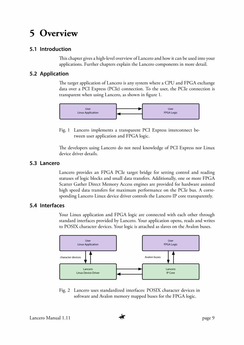
Application5.2 #e target application of Lancero is any system where a CPU and FPGA exchange data over a PCI Express (PCIe) connection. To the user, the PCIe connection is transparent when using Lancero, as shown in "gure 1.
UserLinux Application
UserFPGA Logic
Lancero implements a transparent PCI Express interconnect be-Fig. 1 tween user application and FPGA logic.
#e developers using Lancero do not need knowledge of PCI Express nor Linux device driver details.
Lancero5.3 Lancero provides an FPGA PCIe target bridge for setting control and reading statuses of logic blocks and small data transfers. Additionally, one or more FPGA Scatter Gather Direct Memory Access engines are provided for hardware assisted high speed data transfers for maximum performance on the PCIe bus. A corre-sponding Lancero Linux device driver controls the Lancero IP core transparently.
Interfaces5.4 Your Linux application and FPGA logic are connected with each other through standard interfaces provided by Lancero. Your application opens, reads and writes to POSIX character devices. Your logic is attached as slaves on the Avalon buses.
LanceroLinux Device Driver
LanceroIP Core
UserLinux Application
UserFPGA Logic
Avalon busescharacter devices
Lancero uses standardized interfaces: POSIX character devices in Fig. 2 software and Avalon memory mapped buses for the FPGA logic.
page 10 Lancero Manual 1.11
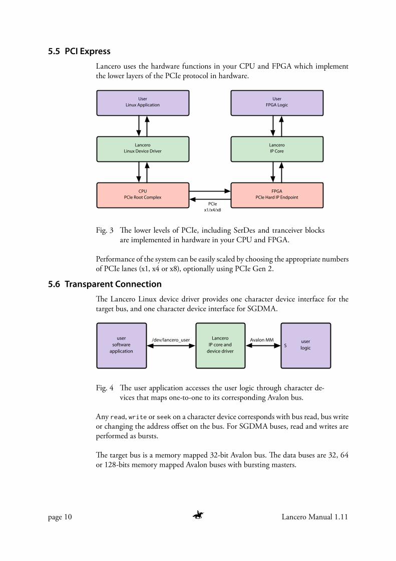
PCI Express5.5 Lancero uses the hardware functions in your CPU and FPGA which implement the lower layers of the PCIe protocol in hardware.
LanceroLinux Device Driver
CPUPCIe Root Complex
FPGAPCIe Hard IP Endpoint
LanceroIP Core
PCIex1/x4/x8
UserLinux Application
UserFPGA Logic
#e lower levels of PCIe, including SerDes and tranceiver blocks Fig. 3 are implemented in hardware in your CPU and FPGA.
Performance of the system can be easily scaled by choosing the appropriate numbers of PCIe lanes (x1, x4 or x8), optionally using PCIe Gen 2.
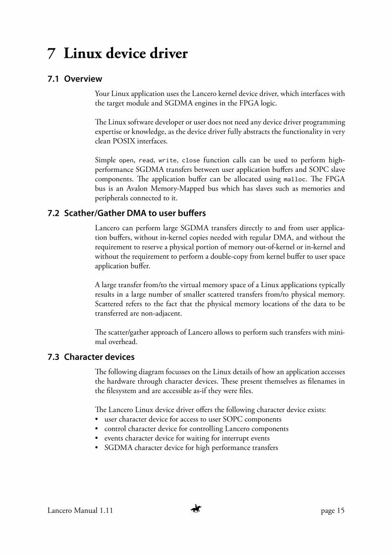
Transparent Connection5.6 #e Lancero Linux device driver provides one character device interface for the target bus, and one character device interface for SGDMA.
LanceroIP core and
device driver
usersoftware
application
userlogicS
/dev/lancero_user Avalon MM
#e user application accesses the user logic through character de-Fig. 4 vices that maps one-to-one to its corresponding Avalon bus.
Any read, write or seek on a character device corresponds with bus read, bus write or changing the address o!set on the bus. For SGDMA buses, read and writes are performed as bursts.
#e target bus is a memory mapped 32-bit Avalon bus. #e data buses are 32, 64 or 128-bits memory mapped Avalon buses with bursting masters.

Lancero Manual 1.11 page 11
Lancero IP core6 SOPC module6.1
#e Lancero IP core is delivered as a ready-to-use module for SOPC Builder. Two modules con"gurations are available; Target and SGDMA.
Target Module6.1.1
#e Target Module con"guration is ideal for small PCIe end points which just re-quire simple register access and where cost and resources are limited. #is includes an interrupt controller.
SGDMA Module Read/Write6.1.2
#e SGDMA Module con"guration additionally provides Scatter-Gather Direct Memory Access engines for applications where high data rates are required. #is also includes the target bridge and interrupt controller.
SGDMA Module Read6.1.3
For applications where the data %ow is towards the FPGA endpoint only. #is also includes the target bridge and interrupt controller.
SGDMA Module Write Only6.1.4
For applications where the data %ow is towards the CPU host only. #is also in-cludes the target bridge and interrupt controller.
Resources6.2 Table 1 shows the performance and resource utilization of Lancero:
Device Con!guration Logic Memory(M9K)
fmax (MHz)
Cyclone IV GX(x1/x4)
Lancero Bridge 1352 LEs 11 >125Lancero SGDMA write 3388 LEs 18Lancero SGDMA read 3927 LEs 21Lancero SGDMA both 5905 LEs 28
Arria II GX orStratix IV GX (x1/x4)
Lancero Bridge 592 ALMs 9 >125Lancero SGDMA write 1491 ALMs 18Lancero SGDMA read 1722 ALMs 20Lancero Scatter Gather 2594 ALMs 27
Arria II GX orStratix IV GX (x8)
Lancero Bridge 680 ALMs 17 >250Lancero SGDMA write 1649 ALMs 32Lancero SGDMA read 1942 ALMs 32Lancero Scatter Gather 2834 ALMs 43
Lancero supports a full speed interconnect with the PCIe IP core at 125 MHz even on the slowest speed grade Cyclone IV.

page 12 Lancero Manual 1.11
SOPC Block diagram6.3
PCIEBridge
PCIE
UD
Mux
PCIE
DU
Mux
PCIETargetBridge
PCIEDesc
Bridge
PCIESGDMAwrite
PCIESGDMAread
PCIECFG
PCIEIRQ
Lancero SGDMA
Avalon ST
Avalon MM, 32-bit
Avalon burst MM, 64-bit
0x0000
(BAR1)
DSCUDMux
DSCDUMux
0x0100
(BAR1)
0x0200
(BAR1)
0x0400
(BAR1)
PCIESGDMAreadperf
0x0500
(BAR1)
PCIESGDMAwrite perf
0x0300
(BAR1)
BAR0
IRQ 0-15
amm_tar
amm_wdma
amm_rdma
Lancero block diagram showing the internal SOPC components of Fig. 5 the Lancero Scatter-Gather con"guration.
Lancero is a modular system which can be used with the system-on-programmable-chip (SOPC) Builder to construct your application logic.
PCIe Bridge6.4 #e PCIe bridge is the interface between the Lancero modules and the PCIe sub-system. It connects directly to the Altera PCI Express Hard IP core using the 64-bit wide Avalon streaming interface (Avalon ST).
Target Bridge6.5 Single read and write requests from the PCIe host are translated to Avalon memory mapped bus transactions by the target bridge. #e target bridge is master on the 32-bit memory-mapped Avalon bus. It supports byte, half-word and word transac-tions with natural alignment.
Additional Lancero components and/or user custom logic are connected to the target bus as Avalon slaves for purposes of control and status.
#is o!ers full compatibility with the extending range of Avalon and SOPC build-ing blocks.
Scatter Gather Direct Memory Access Engines6.6 #e SGDMA engines perform all the work to achieve high-speed direct memory access to the host (or other remote devices if a PCIe switch is used). #e engines are slaves on the target bus. #ey can be instructed to perform one or more transfers by setting a few control registers. After the engine starts it works autonomously until completion.

Lancero Manual 1.11 page 13
Data is transfered between the PCIe host and a slave component on a 32, 64 or 128-bit Avalon Memory-Mapped bus connected to the engine. Each engine is an Avalon master on its bus and has burst support.
Each data bus has its own address space.
#e amm_rdma and amm_wdma data buses can be interconnected to form a single bus if this suits the application.
Features6.6.1
Avalon 32, 64, or 128-bit memory mapped bus for data transfers.Burst support on the Avalon bus.Unlimited number of transfers in the descriptor list.Each transfer can be from 8 bytes up to ~2 GB (231 – 8 bytes).New transfers can be added in-%ight.Transfer descriptors are prefetched resulting in no idle latency.
Descriptor Lists6.7 #e transfer work performed by the SGDMA engines is described in a list of transfers called a descriptor list. Each entry in this list describes a memory content transfer between consecutive addresses in both the local and remote address space.
Descriptor lists are created by the initiator of a SGDMA transfer in the initiator memory, which is remote to the FPGA.
Features6.7.1
Unlimited descriptor list size.Read-only speci"cation for a clear separation of work and result. No write over-head is involved during descriptor processing other than the interrupt message on completion.
Descriptor Processor6.8 #e descriptor processor assists the SGDMA engine. It is internal to Lancero and has no accessible interfaces. It is described here for completeness.
#e descriptor processor fetches the descriptor list items from remote memory.
It is controlled by its associated SGDMA engine using a memory mapped Avalon interconnect where the engine is the master and the list processor is the slave.
Features6.8.1
Prefetches descriptors so that the SGDMA engine is never idle during process-ing the transfers in the list.Supports prefetching of up to sixteen descriptors in a single request.

page 14 Lancero Manual 1.11
Interrupt Controller6.9 #e interrupt controller signals the root complex about events by meaning of a PCIe Message Signaled Interrupt (MSI) or a Legacy Interrupt.
#e interrupt controller accepts up to sixteen interrupt sources. Each of the Lancero SGDMA engines is a source. Additional custom user logic (either SOPC or exter-nal) interrupt sources can be connected to the controller.
Features6.9.1
Enable maskEvent MaskRequest maskSixteen interrupt sources from user SOPC components.
Lancero Manual 1.11 page 15
Linux device driver7 Overview7.1
Your Linux application uses the Lancero kernel device driver, which interfaces with the target module and SGDMA engines in the FPGA logic.
#e Linux software developer or user does not need any device driver programming expertise or knowledge, as the device driver fully abstracts the functionality in very clean POSIX interfaces.
Simple open, read, write, close function calls can be used to perform high-performance SGDMA transfers between user application bu!ers and SOPC slave components. #e application bu!er can be allocated using malloc. #e FPGA bus is an Avalon Memory-Mapped bus which has slaves such as memories and peripherals connected to it.
Scather/Gather DMA to user bu"ers7.2 Lancero can perform large SGDMA transfers directly to and from user applica-tion bu!ers, without in-kernel copies needed with regular DMA, and without the requirement to reserve a physical portion of memory out-of-kernel or in-kernel and without the requirement to perform a double-copy from kernel bu!er to user space application bu!er.
A large transfer from/to the virtual memory space of a Linux applications typically results in a large number of smaller scattered transfers from/to physical memory. Scattered refers to the fact that the physical memory locations of the data to be transferred are non-adjacent.
#e scatter/gather approach of Lancero allows to perform such transfers with mini-mal overhead.
Character devices7.3 #e following diagram focusses on the Linux details of how an application accesses the hardware through character devices. #ese present themselves as "lenames in the "lesystem and are accessible as-if they were "les.
#e Lancero Linux device driver o!ers the following character device exists:user character device for access to user SOPC componentscontrol character device for controlling Lancero componentsevents character device for waiting for interrupt eventsSGDMA character device for high performance transfers

page 16 Lancero Manual 1.11
Lancerodevicedriver
usersoftwareapplication
LanceroSGDMA
userSOPClogic
M
M
S
S
S
/dev/lancero_events
/dev/lancero_sgdma
250:0
251:0
LanceroTarget
M
IRQ IRQ
249:0
/dev/lancero_user
/dev/lancero_control
248:0
#e relationship between character devices, major and minor device Fig. 6 numbers and Avalon Memory-Mapped buses and interrupts.
Each character device appears in the "lesystem as a named device node; the name can be chosen by the user or a user application such as ‘udev’.
In turn, the device node refers to a device major and minor number, chosen by the operating system, the device driver or the user through a device driver option.
First time setup7.4 Make sure the FPGA is con"gured before the bootloader and/or Linux runs.
From the Linux command line shell, use the lspci command from the pcitools package to verify that your Linux system has recognized the PCIe end point. You should see the vendor and product ID you have chosen in the Altera PCIe Compiler MegaWizard. By default these are 0x1172 resp. 0x0004.
You may need to reset the system if the FPGA was con"gured after booting Linux and does not show up in the list of PCI devices.
Load the device driver7.4.1
#e lancero.ko "le is the Linux device driver (‘ko’ is for kernel object).
sudo insmod ./lancero.ko
Use the dmesg command to see the output of the device driver and note the major minor numbers for the character devices if this is your "rst setup. For example:
lancero_user = 251:0lancero_control = 250:0lancero_events = 249:0lancero_sgdma = 248:0
Lancero Manual 1.11 page 17
Create the !lesystem device nodes7.4.2
#e device nodes allows your applications to access the character devices as if it were "les. On a persistent storage device for the root "lesystem this needs to be done once. Using the example above:
sudo mknod -m 0666 /dev/lancero_user c 251 0sudo mknod -m 0666 /dev/lancero_control c 250 0sudo mknod -m 0666 /dev/lancero_events c 249 0sudo mknod -m 0666 /dev/lancero_sgdma c 248 0
248-251 are the major number and 0 is the minor number assigned to the device driver, which can be seen from the output of dmesg after loading the driver module (see above).
Static device node7.4.3
In a typical system you want control over the major and minor device node num-bers. #is can be achieved by adding the major= parameter to the driver, with the matching creation of device nodes is (verify with the dmesg command):
sudo insmod ./lancero.ko major=130
sudo mknod -m 0666 /dev/lancero_user c 130 0sudo mknod -m 0666 /dev/lancero_control c 130 1sudo mknod -m 0666 /dev/lancero_events c 130 2sudo mknod -m 0666 /dev/lancero_sgdma c 130 3
Managed dynamic device node7.4.4
As an alternative, most Linux system allow managed on-demand creation of device nodes through a user daemon such as udev.
Interfacing with the device driver7.5 #e Lancero device driver uses a standard POSIX compliant interface using the open, read, write, seek and close calls, which act on the Lancero character de-vices.
Additionally, the target bus character devices supports mmap.
For advanced use, the SGDMA bus characters device support the asynchronous variants of read, write. Currently, this requires the use of the libaio library.
Function call summary7.5.1 ssize_t read(int fildes, void *buf, size_t nbyte);ssize_t write(int fildes, const void *buf, size_t nbyte);off_t lseek(int fildes, off_t offset, int whence);
Variant function calls:
ssize_t pread(int fildes, void *buf, size_t nbyte, off_t offset);ssize_t pwrite(int fildes, const void *buf, size_t nbyte, off_t offset);

page 18 Lancero Manual 1.11
ssize_t readv(int fildes, const struct iovec *iov, int iovcnt);ssize_t writev(int fildes, const struct iovec *iov, int iovcnt);
Advanced use:
void *mmap(void *addr, size_t len, int prot, int flags,
int fildes, off_t off);
Interfacing with the target bus7.6
Read / write size7.6.1
One, two and four byte (nbytes) read and write access is supported.
Alignment7.6.2
All accesses must be naturally aligned. When using read and write calls the "le o!set (offset) must be a multiple of the size (nbytes).
When using mmap() the user application can directly access the target bus using memory access. #e developer and user application are responsible for checking correct alignment.
Return codes7.6.3
-EPROTO indicates misaligned access or invalid length.
Interfacing with the event bus7.7
Read only7.7.1
#e event (virtual) bus is read-only. Only four byte (32-bit) reads are supported (nbytes=4). A read blocks until the interrupt events register has changed since the last read.
Interfacing with the SGDMA bus7.8
Read / write size7.8.1
#e smallest read / write size is equal to the DMA Avalon bus data width, , which is con"gured in the Lancero IP core and can be found by inquiring the Lancero Con"guration Inspector.
Alignment7.8.2
All read/write accesses must be naturally aligned to the DMA Avalon bus data width, thus the "le o!set (offset) and bu!er address (buf) and size (nbytes) both must be a multiple of the data bus width.
Return codes7.8.3
-EPROTO indicates misaligned access or invalid length.-EIOCBQUEUED indicates succesful queueing of the asynchronous request.
Lancero Manual 1.11 page 19
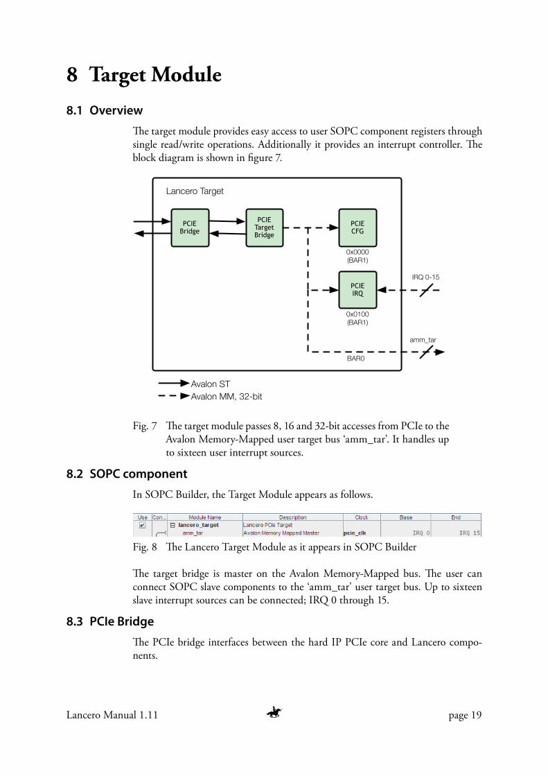
Target Module8 Overview8.1
#e target module provides easy access to user SOPC component registers through single read/write operations. Additionally it provides an interrupt controller. #e block diagram is shown in "gure 7.
PCIEBridge
PCIETargetBridge
PCIECFG
PCIEIRQ
Lancero Target
Avalon ST
Avalon MM, 32-bit
0x0000
(BAR1)
0x0100
(BAR1)
BAR0
amm_tar
IRQ 0-15
#e target module passes 8, 16 and 32-bit accesses from PCIe to the Fig. 7 Avalon Memory-Mapped user target bus ‘amm_tar’. It handles up to sixteen user interrupt sources.
SOPC component8.2 In SOPC Builder, the Target Module appears as follows.
#e Lancero Target Module as it appears in SOPC BuilderFig. 8
#e target bridge is master on the Avalon Memory-Mapped bus. #e user can connect SOPC slave components to the ‘amm_tar’ user target bus. Up to sixteen slave interrupt sources can be connected; IRQ 0 through 15.
PCIe Bridge8.3 #e PCIe bridge interfaces between the hard IP PCIe core and Lancero compo-nents.
page 20 Lancero Manual 1.11
Target Bridge8.4 #e target bridge transparently maps read and write accesses from the PCIe host into corresponding accesses on the local Avalon Memory-Mapped target bus.
#e target bridge has two BAR regions. Lancero components are mapped in BAR1 and user SOPC components are mapped in BAR0.
BAR0 Address Map8.5 #e BAR0 address map fully depends on the user SOPC components.
User Character Device8.6 #e user character device is used to access the user SOPC components in the BAR0 address space connected on the ‘amm_tar’ bus.
#e target control character device accepts 1, 2 or 4-byte read and write calls on 1,2 or 4-byte aligned positions respectively.
Application example; write to a user SOPC component register8.6.1
uint32_t value = 0x00084321;uint32_t register_address = 0x8000;int fd = open(”/dev/lancero_user”, O_RDWR);int rc = pwrite(fd, &value, 4, register_address);close(fd);
Two variables are initialized with the value and register address to be set. In the open call, the user character device that corresponds with the target user bus on the FPGA is opened. A "le descriptor is returned. You can now access this device like a "le. With the pwrite call, a positional write of the 4-byte value 0x00084321 is performed to address 0x00008000 on the Avalon target bus.
Mapping the user bus in memory8.6.2
Additionally, the user character device supports mmap, through which the target bus can be mapped into the application virtual memory area. #e application can then use memory access to read and write through the target bus. #is method has less system overhead than the read/write() approach. However, the user is responsible for proper accesses regarding address range, size and alignment.
BAR1 Address Map8.7 #e base addresses for the Lancero components in BAR1 are as follows.
Description Target Bus Base Address (–End Address)Con"guration 0x000 (–0x0FF)Interrupt Controller 0x100 (–0x1FF)
Single byte (8 bit), half-word (16 bit) and word (32 bit) memory read and write ac-cesses are supported. #ese are transparently translated into similar accesses on the

Lancero Manual 1.11 page 21
target bus. #e accesses must use natural alignment. For example: a 16-bit access must be on an even byte address.
Control Character Device8.8 #e control character device is used to acces the Lancero components on BAR1.#e same access restrictions apply as with the user character device (see above).
Con!guration Inspector8.9 #e con"guration inspector is used to query the Lancero module con"guration.
Register Map8.9.1
#e con"guration inspector is located at base address 0x0 and has the following registers for identi"cation and control:
Byte O"set Name RC access EP access Description0x00 identi"er R R Identi"er and Version0x04 bus_dev_fn R W Bus, device and function0x08 payload R W Payload0x0C maxread R W Maximum read request (bytes)0x10 lancero_id R W Lancero System Identi"er0x14 msi R W MSI0x18 pcie_width R W PCIe Hard IP Avalon ST width0x1c wdma width R W Write DMA Avalon MM width0x20 rdma width R W Read DMA Avalon MM width
All registers support 32-bit (PCI DWORD) access only.
Identi!er and Version Register8.9.2
#is read-only "xed-value register allows the device driver to verify that the con-"guration inspector component is available, and which version it is.
Identi!er and Version Register31:24 23:8 7:0Reserved Identi"er Version
Identi!er Value Description0xB200 Con"guration Inspector Identi"erother values Reserved
#e version value indicates the con"guration inspector module version. Some reg-isters are only available since a speci"c version.
Version Value Description0x01 Con"guration Inspector version 10x02 Con"guration Inspector version 2other values Reserved

page 22 Lancero Manual 1.11
Bus Device Function register8.9.3
Bit Name RC access Description
31:16 Reserved R Reserved15:8 bus R Bus number7:3 device R Device number2:0 function RW Function number
Payload register8.9.4
#e maximum PCI Express payload is con"gurable in both the PCI Express Meg-awizard and the Lancero SOPC component. #e actual payload used is determined by the host system and it can be read by this register.
Bit Name RC access Description
31:13 Reserved R Reserved12:0 payload R PCIe TLP payload size in bytes
Maximum Read Request register8.9.5
Bit Name RC access Description
31:13 Reserved R Reserved12:0 maxread R PCIe Maximum Read Request in bytes
Lancero System Identi!er register8.9.6
Indicates the Lancero system in use:Bit Name RC access Description
31:16 Reserved R Reserved15:0 lancero_id R Lancero System Identi"er
Lancero System Identi!er Value Description0xFF01 Lancero Target0xFF02 Lancero SGDMA0xFF03 Lancero SGDMA Write Onlyother values Reserved
Message Signaled Interrupt (MSI) register8.9.7
#is register appeared in version 2 of the Lancero IP Speci"cation.Bit Name RC access Description
31:1 Reserved R Reserved0 msien R 1 = MSI Enabled, 0= Legacy Interrupting Enabled

Lancero Manual 1.11 page 23
#e use of Message Signaled Interrupts is con"gured using PCI Express con"gura-tion registers.
PCIe IP Avalon Width register8.9.8
#is register appeared in version 2 of the Lancero IP Speci"cation.Bit Name RC access Description
31:2 Reserved R Reserved1 pcie_128 R 128 bits PCIe Avalon width0 pcie_64 R 64 bits PCIe Avalon width
Indicates the data bus width between Lancero and the PCIe IPs.
Write DMA Avalon Width register8.9.9
#is register appeared in version 2 of the Lancero IP Speci"cation.Bit Name RC access Description
31:5 Reserved R Reserved4 wdma_256 R 256 bits write DMA Avalon bus data width3 wdma_128 R 128 bits write DMA Avalon bus data width2 wdma_64 R 64 bits write DMA Avalon bus data width1 wdma_32 R 32 bits write DMA Avalon bus data width0 wdma_en R write DMA is enabled and available
Indicates the data bus width available to the user from the Lancero IP core.
Read DMA Avalon Width register8.9.10
#is register appeared in version 2 of the Lancero IP Speci"cation.Bit Name RC access Description
31:5 Reserved R Reserved4 rdma_256 R 256 bits read DMA Avalon bus data width3 rdma_128 R 128 bits read DMA Avalon bus data width2 rdma_64 R 64 bits read DMA Avalon bus data width1 rdma_32 R 32 bits read DMA Avalon bus data width0 rdma_en R read DMA is enabled and available
Indicates the data bus width available to the user from the Lancero IP core.
Interrupt Controller8.10 Whenever the hardware needs to signal the software it will raise an interrupt re-quest. Software then needs to determine the cause of the interrupt and determine which action to take and when.
#e interrupt controller has 24 interrupt sources. #e upper eight (23-16) are internal to Lancero. #e others interrupts (15-0) are available for user SOPC com-
page 24 Lancero Manual 1.11
ponents. Whenever an interrupt occurs and is enabled in the enable register, a PCIe interrupt is sent.
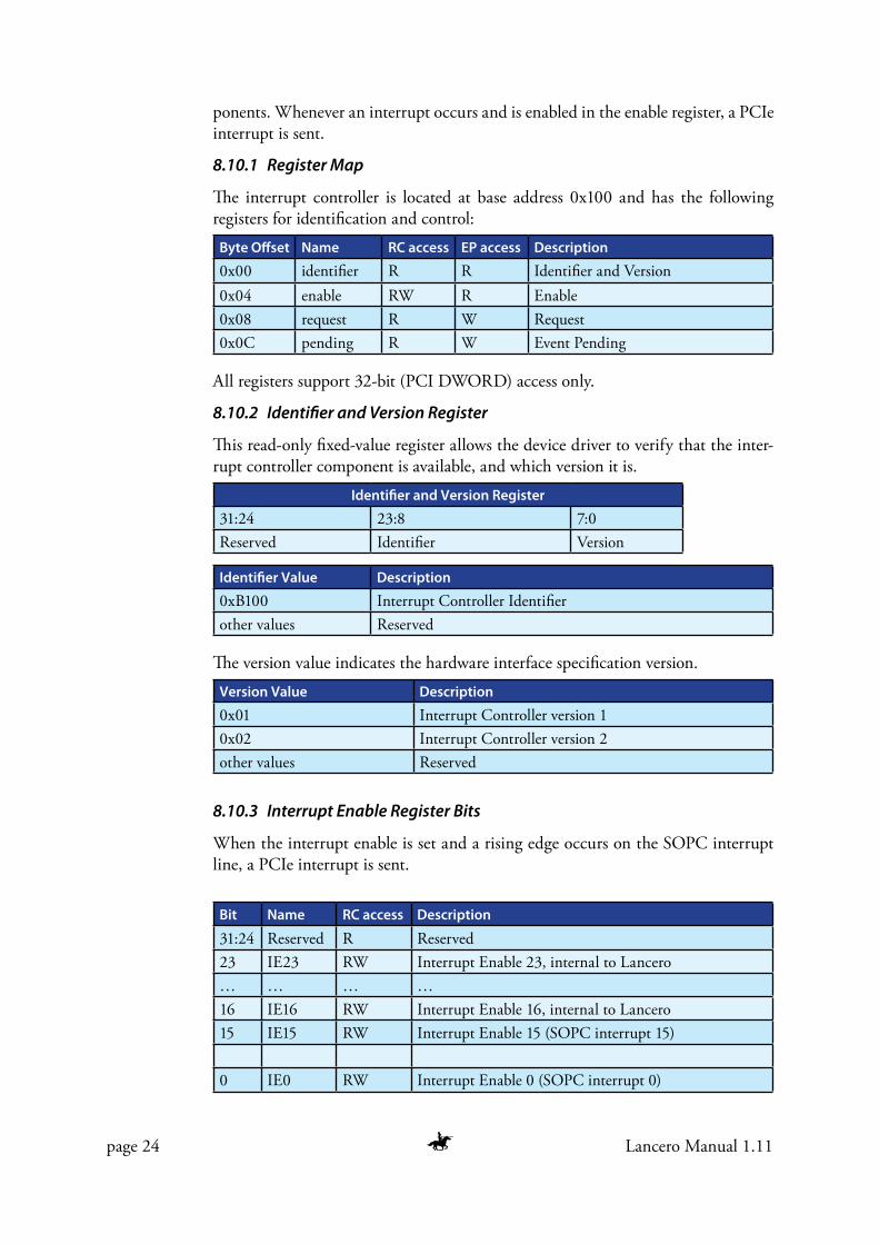
Register Map8.10.1
#e interrupt controller is located at base address 0x100 and has the following registers for identi"cation and control:
Byte O"set Name RC access EP access Description0x00 identi"er R R Identi"er and Version0x04 enable RW R Enable0x08 request R W Request0x0C pending R W Event Pending
All registers support 32-bit (PCI DWORD) access only.
Identi!er and Version Register8.10.2
#is read-only "xed-value register allows the device driver to verify that the inter-rupt controller component is available, and which version it is.
Identi!er and Version Register31:24 23:8 7:0Reserved Identi"er Version
Identi!er Value Description0xB100 Interrupt Controller Identi"erother values Reserved
#e version value indicates the hardware interface speci"cation version.Version Value Description0x01 Interrupt Controller version 10x02 Interrupt Controller version 2other values Reserved
Interrupt Enable Register Bits8.10.3
When the interrupt enable is set and a rising edge occurs on the SOPC interrupt line, a PCIe interrupt is sent.
Bit Name RC access Description
31:24 Reserved R Reserved23 IE23 RW Interrupt Enable 23, internal to Lancero… … … …16 IE16 RW Interrupt Enable 16, internal to Lancero15 IE15 RW Interrupt Enable 15 (SOPC interrupt 15)
0 IE0 RW Interrupt Enable 0 (SOPC interrupt 0)

Lancero Manual 1.11 page 25
Interrupt Request Register Bits8.10.4
IR0 through IR23 indicate the current interrupt source lines ANDed with the enable mask. #e interrupts must be cleared by deasserting the source.
Bit Name RC access Description
31:24 Reserved R Reserved23 IE23 RW Interrupt Request 23, internal to Lancero… … … …16 IE16 RW Interrupt Request 16, internal to Lancero15 IE15 RW Interrupt Request 15 (SOPC interrupt 15)
0 IE0 RW Interrupt Enable 0 (SOPC interrupt 0)
Interrupt Event Pending Register Bits8.10.5
EP0 through EP23 indicate the current interrupt source lines indicating pending events. #e events must be cleared by removing the event cause condition in the source component.
Bit Name RC access Description
31:24 Reserved R Reserved23 EP23 R Interrupt Event Pending 23, internal to Lancero… … … …16 EP16 R Interrupt Event Pending 16, internal to Lancero15 EP15 R Interrupt Event Pending 15 (SOPC interrupt 15)
0 EP0 R Interrupt Event Pending 0 (SOPC interrupt 0)
#e interrupt events pending register "rst appeared in version 2 of the interrupt controller.
Interrupt Event Character Device8.11 #e event character device is a convenience interface; it allows the application to perform a blocking read waiting for an interrupt event to occur, without polling the interrupt request register of the interrupt controller. #e character device accepts only 4-byte read calls.
Whenever the character device is read, the read blocks until the interrupt request bit vector was changed since the last read.
#e user application is responsible for clearing the pending interrupts by removing the interrupt cause condition in the respective Avalon slaves.
page 26 Lancero Manual 1.11
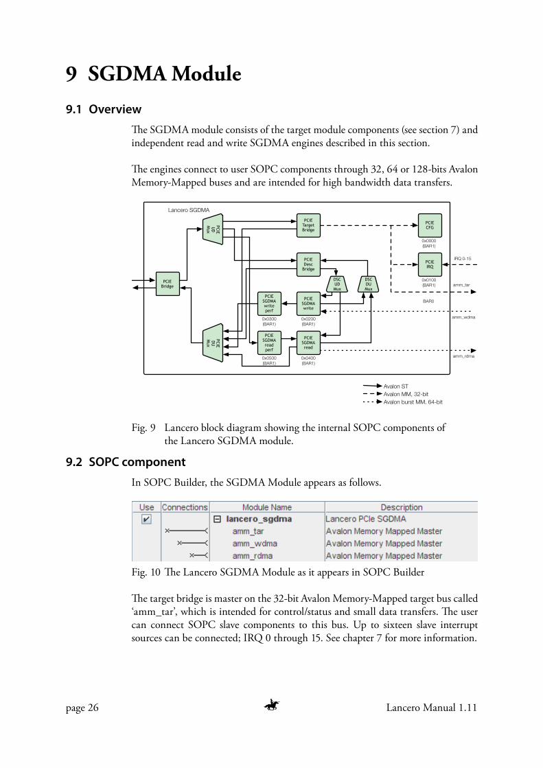
SGDMA Module9 Overview9.1
#e SGDMA module consists of the target module components (see section 7) and independent read and write SGDMA engines described in this section.
#e engines connect to user SOPC components through 32, 64 or 128-bits Avalon Memory-Mapped buses and are intended for high bandwidth data transfers.
PCIEBridge
PCIE
UD
Mux
PCIE
DU
Mux
PCIETargetBridge
PCIEDesc
Bridge
PCIESGDMAwrite
PCIESGDMAread
PCIECFG
PCIEIRQ
Lancero SGDMA
Avalon ST
Avalon MM, 32-bit
Avalon burst MM, 64-bit
0x0000
(BAR1)
DSCUDMux
DSCDUMux
0x0100
(BAR1)
0x0200
(BAR1)
0x0400
(BAR1)
PCIESGDMAreadperf
0x0500
(BAR1)
PCIESGDMAwrite perf
0x0300
(BAR1)
BAR0
IRQ 0-15
amm_tar
amm_wdma
amm_rdma
Lancero block diagram showing the internal SOPC components of Fig. 9 the Lancero SGDMA module.
SOPC component9.2 In SOPC Builder, the SGDMA Module appears as follows.
#e Lancero SGDMA Module as it appears in SOPC BuilderFig. 10
#e target bridge is master on the 32-bit Avalon Memory-Mapped target bus called ‘amm_tar’, which is intended for control/status and small data transfers. #e user can connect SOPC slave components to this bus. Up to sixteen slave interrupt sources can be connected; IRQ 0 through 15. See chapter 7 for more information.

Lancero Manual 1.11 page 27
#e SOPC component can be con"gured by double-clicking it. #e con"guration GUI will appear as shown in "gure 11. #e PCIe Data Width, Maximum Payload and Maxium Read Request must match the PCIe Hard IP Megawizard settings.
#e SGDMA (Avalon Bus) Data Widths are user con"gurable.
#e Lancero con"guration GUI in SOPC BuilderFig. 11
#e SGDMA write engine has a 32, 64 or 128-bits Avalon Memory-Mapped bus called ‘amm_wdma’ which performs writes to the PCIe host. #e user can connect SOPC slave components to this bus for high performance data transfers. #e bus supports burst tranfers. #e write engine is controlled through the Target Bridge.
#e SGDMA read engine has a 64-bit Avalon Memory-Mapped bus called ‘amm_rdma’ which performs reads from the PCIe host. #e user can connect SOPC slave components to this bus for high performance data transfers. #e bus supports burst tranfers. #e read engine is controlled through the Target Bridge.
BAR1 Address Map9.3 #e Lancero components, including the SGDMA engines, are controlled through the target bus using BAR1. #e base addresses for the Lancero components are:

page 28 Lancero Manual 1.11
Description Target Bus Base Address (–End Address)Con"guration 0x000 (–0x0FF)Interrupt Controller 0x100 (–0x1FF)SGDMA Write Engine 0x200 (–0x2FF)SGDMA Read Engine 0x400 (–0x4FF)
For the register map of the con"guration controller and the interrupt controller see section 7.
SGDMA Read and Write Engine9.4 An SGDMA engine transfers data between the local Avalon Memory-Mapped bus and the remote memory in the PCIe host.
#e transfers are speci"ed in a transfer descriptor list which are constructed by (driver) software in PCIe host memory. After this list is available, the PCIe host address of this list is set in an engine control register. #e engine is then started.
#e engine will autonomously prefetch the descriptors and perform the speci"ed transfers. During its operation new transfers can be added to the list.
Write Engine9.4.1
#e write engine transfers data from the user SOPC component(s) on its Avalon Memory-Mapped bus to the PCIe host.
#e write engine performs burst reads on the Avalon bus and performs (posted) memory writes on the PCIe bus. It
Read Engine9.4.2
#e read engine transfers data from the PCIe host to the user SOPC component(s) on the 64-bit Avalon Memory-Mapped bus.
#e read engine is an initiator of (non-posted) memory reads on the PCIe bus. It performs burst writes on the Avalon data bus.
SGDMA Character Device9.5 #e SGDMA character device is used to perform high-speed SGDMA transfers between the PCIe host and the user SOPC components on the amm_rdma and amm_wdma buses.
Standard I/O9.5.1
#e SGDMA character device accepts read and write requests for any size which is a multiple of its data bus width, and to/from addresses that are aligned with its data bus width. Each I/O request results in one or more SGDMA transfers. After

Lancero Manual 1.11 page 29
the transfer completes, the read and write returns the number of bytes transferred, or a negative error code in case of errors.
#e read and write engines work independently; read requests are handled in order of submission and write request are handled in order of submission.
When using the normal (blocking, synchronous) I/O request the SGDMA engines will be idle during setup and completion of the transfers. In order to achieve maxi-mum performance, see the advanced I/O topic below.
Example: Transfer data from FPGA to application bu"er using SGDMA9.5.2
#define BUF_SIZE (1024 * 1024)char *buffer = (char *)malloc(BUF_SIZE);int fd = open(”/dev/lancero_sgdma”, O_RDWR);int rc = read(fd, buffer, BUF_SIZE);close(fd);
Using malloc a bu!er of one Megabyte is allocated. Note that this bu!er appears as one contiguous block in the application virtual address space but very likely lies scattered throughout the physical memory attached to the processor.
In the open call, the character device that corresponds with the SGDMA data bus on the FPGA is opened. A "le descriptor is returned. You can now access this device like a "le.
With the read call, one Megabyte is requested to be transferred from the device to the application bu!er. During this call, the device driver will prepare and then initiate the transfer in hardware. #e processor will be freed to run other tasks on your Linux system, while the driver waits for the hardware to "nish. After the hardware "nishes the transfer, the application continues and “transfer completed.” is printed.
Advanced I/O9.5.3
Multiple threads or applications can submit I/O requests simultaneously and trans-parently.
Additionally, the character device supports asynchronous read and write requests, which requires using the Linux libaio library.
When performing overlapping I/O by using multiple threads or asynchronous I/O requests, the transfers are handled back-to-back by the Lancero Linux driver and IP core, achieving maximum performance.
SGDMA Engine Register Map9.6 Each SGDMA engine is controlled through its Avalon slave interface on the target bus.

page 30 Lancero Manual 1.11
Note: #e Lancero Linux device driver hides the control from the user. #e infor-mation below is needed only if the user is developing custom drivers or software to control the SGDMA engines.
#e SGDMA engine control interface consists of seven 32-bit registers:Byte O"set Name RC access EP access Description0x00 identi"er R R Identi"er and Version0x04 status R W Status0x08 control R/W R Control0x0C "rst_desc R/W R First descriptor bus address0x10 "rst_desc_
adjacentR/W R Number of descriptors in memory
adjacent after the "rst descriptor.0x14 completed_
desc_countR W Number of completed descriptors,
updated by the engine after comple-tion of each descriptor in the list.
0x18 completed_ desc_bytes
R W Number of bytes transferred of the transfer related with the descriptor the engine is processing, updated by the engine during the transfer.
0x1c Reserved R/W R Must be set to zero (0).
All registers support 32-bit (PCI DWORD) access only.
#e "rst_desc and "rst_desc_adjacent registers must be written before starting the engine.
Identi!er and Version Register9.6.1
#is read-only "xed-value register allows the device driver to verify that the SGDMA engine component is available, and which version it is.
Identi!er and Version Register31:24 23:8 7:0Reserved Identi"er Version
#e identi"er value indicates the variant of SGDMA engine, read or write.Identi!er Value Description0xC200 SGDMA Read Engine with Avalon Memory Master Bus0xC100 SGDMA Write Engine with Avalon Memory Master Busothers Reserved
#e version value indicates the hardware interface speci"cation versionVersion Value Description0x01 SGDMA Engine version 10x02 SGDMA Engine version 2others Reserved

Lancero Manual 1.11 page 31
Status Register9.6.2
#e status register indicates the current state of the SGDMA engine. #e bits are set and reset by the SGDMA engine and are read-only.
Bit Name RC access Description
0 BUSY R One (1) if the SGDMA engine is busy, zero (0) when it is idle.
1 DESCRIPTOR_ STOPPED
R Reset (0) on setting RUN_STOP (1). Set (1) after the engine completed a descriptor with the STOP bit set.
2 DESCRIPTOR_COMPLETED
R Reset (0) on setting RUN_STOP (1). Set (1) after the engine completed a descriptor.
3 RESERVED R Reserved4 MAGIC_
STOPPEDR Reset (0) on setting RUN_STOP (1). Set (1)
when the engine encountered a descriptor with invalid magic and stopped. #is indicates memory corruption and/or a software bug.
5 FETCH_STOPPED
R Reset (0) on setting RUN_STOP (1). Set (1) when the engine could not fetch a descriptor due to a PCI Express completion timeout. #is indicates a hardware problem or software miscon"guration.
6 IDLE_STOPPED R Reset (0) on setting RUN_STOP (1). Set (1) when the engine stopped after resetting RUN_STOP (0).
7 PAYLOAD_ MISMATCH
R (Re)set during PCIe con"guration. Set (1) when the system payload is larger than Lancero was con"gured for in SOPC Builder. #is might decrease write engine performance.
8 MAXREAD_ MISMATCH
R (Re)set during PCIe con"guration. Set (1) when the system maxread is larger than Lancero was con"gured for in SOPC Builder. #is might result in read engine data corruption.
9 NONALIGNED_STOPPED
R Reset (0) on setting RUN_STOP (1). Set (1) when the transfer is not aligned properly.
10-31
Reserved R Reserved
Bits 7 through 9 was introduced in version 2 of the SGDMA engine. #ey are zero in older versions.
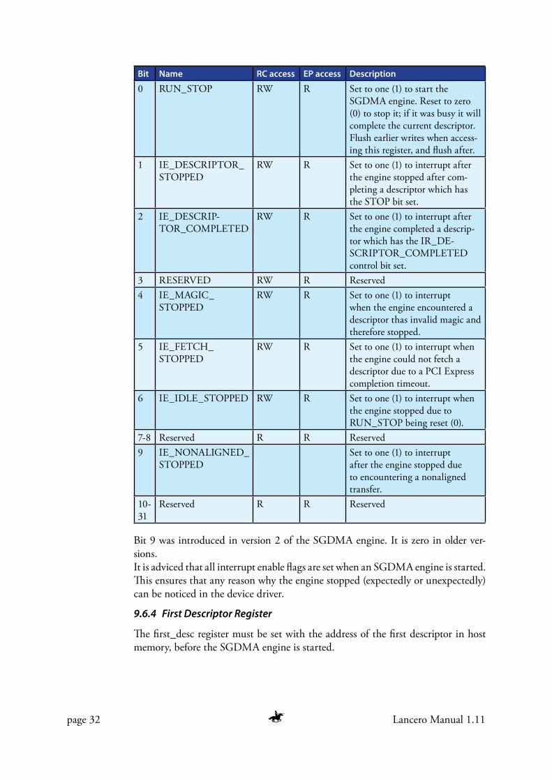
Control Register9.6.3
#e status register indicates the current state of the SGDMA engine. #e bits are set and reset by the SGDMA engine and are read-only.
page 32 Lancero Manual 1.11
Bit Name RC access EP access Description
0 RUN_STOP RW R Set to one (1) to start the SGDMA engine. Reset to zero (0) to stop it; if it was busy it will complete the current descriptor. Flush earlier writes when access-ing this register, and %ush after.
1 IE_DESCRIPTOR_ STOPPED
RW R Set to one (1) to interrupt after the engine stopped after com-pleting a descriptor which has the STOP bit set.
2 IE_DESCRIP-TOR_COMPLETED
RW R Set to one (1) to interrupt after the engine completed a descrip-tor which has the IR_DE-SCRIPTOR_COMPLETED control bit set.
3 RESERVED RW R Reserved4 IE_MAGIC_
STOPPEDRW R Set to one (1) to interrupt
when the engine encountered a descriptor thas invalid magic and therefore stopped.
5 IE_FETCH_STOPPED
RW R Set to one (1) to interrupt when the engine could not fetch a descriptor due to a PCI Express completion timeout.
6 IE_IDLE_STOPPED RW R Set to one (1) to interrupt when the engine stopped due to RUN_STOP being reset (0).
7-8 Reserved R R Reserved9 IE_NONALIGNED_
STOPPEDSet to one (1) to interrupt after the engine stopped due to encountering a nonaligned transfer.
10-31
Reserved R R Reserved
Bit 9 was introduced in version 2 of the SGDMA engine. It is zero in older ver-sions.It is adviced that all interrupt enable %ags are set when an SGDMA engine is started. #is ensures that any reason why the engine stopped (expectedly or unexpectedly) can be noticed in the device driver.
First Descriptor Register9.6.4
#e "rst_desc register must be set with the address of the "rst descriptor in host memory, before the SGDMA engine is started.

Lancero Manual 1.11 page 33
First Descriptor Adjacent Register9.6.5
#e "rst_desc_adj register must be set to 0. (In future releases, this allows prefetch-ing multiple descriptors which are contiguous in memory.)
Descriptor Completed Register9.6.6
#e desc_completed register is read-only and holds the number of descriptors that have been completed by the engine. It is set to zero on the engine BUSY rising edge,and is incremented after each descriptor that was completed. #e value re-mains stable after the engine BUSY %ag falling edge.
SGDMA Descriptor9.7 Each descriptor contains the information for a transfer of a memory area that is contiguous in both the Avalon bus and remote PCIe memory address spaces.
A descriptor has the address of the next descriptor so that a linked list of descriptors can be processed by the SGDMA engine. Each descriptor has %ags to control the engine when it completes processing the descriptor.
Byte O"set
Fields31:16 15:12 11:8 7:0
0x00 magic 0xAD4B reserved(4 bits)
extra_adjacent
control
0x04 length [31:3]0x08 fpga_addr [31:3]0x0C fpga_addr_pad0x10 pcie_addr [31:3]0x14 pcie_addr_pad0x18 next_addr [31:2]0x1C next_addr_pad
Descriptor Fields9.7.1
#e length and address "elds describe a single memory transfer. #e control "eld controls per-transfer actions the engine should take.
A wrong value in the magic "eld protects against software bugs or memory corrup-tion. #e engine will stop with the status MAGIC_STOPPED %ag set.
#e next_addr "eld indicates where the next descriptor is and the extra_adjacent helps to prefetch multiple descriptors in one request.
Byte O"set Name RC access EP access Description0x00 control R/W R Descriptor control %ags.0x01 extra_adjacent R/W R Number of descriptors (0-15)
that are adjacent in memory after the descriptor at next_addr.
0x02 reserved R/W R Reserved. Must be set to zero.
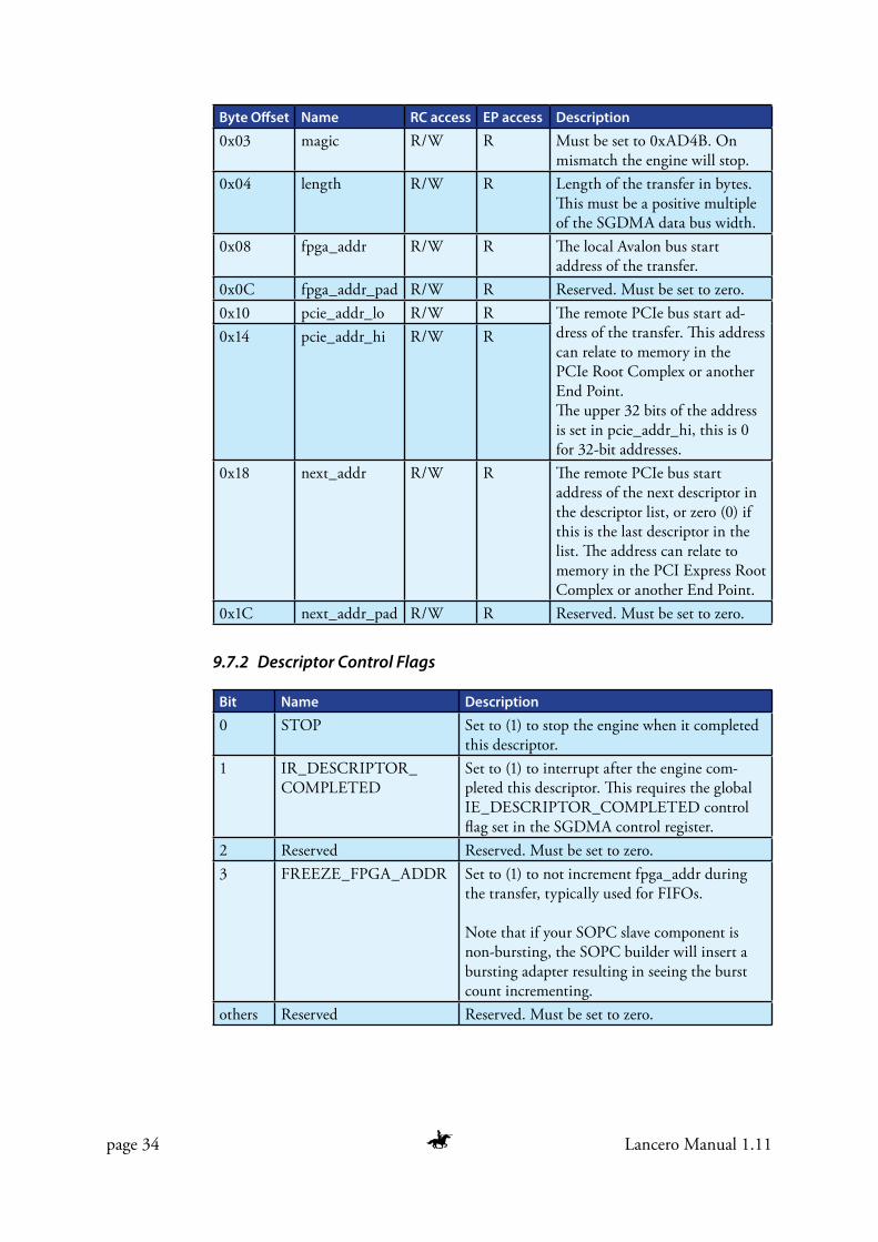
page 34 Lancero Manual 1.11
Byte O"set Name RC access EP access Description0x03 magic R/W R Must be set to 0xAD4B. On
mismatch the engine will stop.0x04 length R/W R Length of the transfer in bytes.
#is must be a positive multiple of the SGDMA data bus width.
0x08 fpga_addr R/W R #e local Avalon bus start address of the transfer.
0x0C fpga_addr_pad R/W R Reserved. Must be set to zero.0x10 pcie_addr_lo R/W R #e remote PCIe bus start ad-
dress of the transfer. #is address can relate to memory in the PCIe Root Complex or another End Point.#e upper 32 bits of the address is set in pcie_addr_hi, this is 0 for 32-bit addresses.
0x14 pcie_addr_hi R/W R
0x18 next_addr R/W R #e remote PCIe bus start address of the next descriptor in the descriptor list, or zero (0) if this is the last descriptor in the list. #e address can relate to memory in the PCI Express Root Complex or another End Point.
0x1C next_addr_pad R/W R Reserved. Must be set to zero.
Descriptor Control Flags9.7.2
Bit Name Description0 STOP Set to (1) to stop the engine when it completed
this descriptor.1 IR_DESCRIPTOR_
COMPLETEDSet to (1) to interrupt after the engine com-pleted this descriptor. #is requires the global IE_DESCRIPTOR_COMPLETED control %ag set in the SGDMA control register.
2 Reserved Reserved. Must be set to zero.3 FREEZE_FPGA_ADDR Set to (1) to not increment fpga_addr during
the transfer, typically used for FIFOs.
Note that if your SOPC slave component is non-bursting, the SOPC builder will insert a bursting adapter resulting in seeing the burst count incrementing.
others Reserved Reserved. Must be set to zero.

Lancero Manual 1.11 page 35
Quick Start Reference Designs10 Deliverables10.1
Lancero is delivered as a "le archive that must be extracted to your workstation. It contains the following:
IPContains the Lancero SOPC Modules.
SynthesisContains the Quartus reference design.
SimulationContains the simulation testbench.
Lancero
DocumentationContains the documentation.
DriverContains the Linux device driver.
Reference Designs10.2 #e reference designs are located in the synthesis directory. #e reference designs have the following hierarchical design structure:
Lancero SOPC
PCI ExpressHard IP
Lancero
Lancero Top
Avalon ST
Top level design of the Lancero reference design.Fig. 12

page 36 Lancero Manual 1.11
#e following designs are readily available:Name Description
alt_a2gx_dex_x1 Altera Arria II GX development board single lanealt_a2gx_dex_x4 Altera Arria II GX development board four lanesalt_a2gx_dex_x4 Altera Arria II GX development board eight lanesalt_c4gx_str_x1 Altera Cyclone IV GX starters kit single laneterasic_de4 Terasic DE4 board eight lanes
Following these step-by-step instructions helps you generate a Lancero reference project:
Add the Lancero OpenCore license to the Quartus license "le.Start Quartus.Open a Lancero project from the ‘synthesis’ directory. Multiple projects are available. For the Arria II GX development board x4 reference design open the lancero_alt_a2gx_dev_x4.qpf "le in the alt_a2gx_dev_x4 directory. For the Cyclone IV GX development kit open the lancero_alt_c4gx_str_x1.qpf "le in the alt_c4gx_str_x1 directory.
#e "rst step is to generate the PCI Express Hard IP core:Open the MegaWizard (Tools —› MegaWizard).Select the option ‘Edit an existing megafunction variation’ and click ‘Next’.Select the "le ‘pcie_hip.v’ and click ‘Next’.Click ‘Finish’ to generate the core.After the PCI Express compiler has "nished, click ‘Exit’ to leave the Wizard.
#e second step is to generate the SOPC Builder system:Start the SOPC Builder (Tools —› SOPC Builder).Initially the Lancero library must be added to the IP search path, this can be found in Tools —› Options. Add the directory ‘IP’.Click on ‘Finish’ to leave the options menu.Click on ‘Generate’ to create the SOPC system.After the system was succesfully generated, click on ‘Exit’ to leave the SOPC Builder.
#e project can now be built.Compile the project (Processing —› Start Compilation).Optionally program the board (Tools —› Programmer).
User Components10.3 #e reference design has some user SOPC components attached to the target bus and SGDMA buses.
On-chip memory attached to target bus10.4 A small on-chip RAM slave is or can be attached to the target bus amm_tar.

Lancero Manual 1.11 page 37
Write tester attached to SGDMA write bus10.5 #e SGDMA amm_wdma bus has a write tester attached to it. #is is an SOPC Avalon Memory-Mapped slave component. When reading from any location in its address space, the write tester returns incremental 32-bit sequence numbers, starting at zero. An internal counter keeps state.
#e purpose of the write tester is to provide the write SGDMA engine with deter-ministic data which can then be tested by the PCIe host after DMA has "nished.
Register Map10.5.1
#e write tester is located at base address 0x1000 and has the following registers for identi"cation and control:
Byte O"set Name RC access EP access Description0x00 identi"er R R Identi"er and Version0x04 control RW R Control
All registers support 32-bit (PCI DWORD) access only.
Identi!er and Version Register10.5.2
#is read-only "xed-value register allows the software to inquire the write tester component.
Identi!er and Version Register31:24 23:8 7:0Reserved Identi"er Version
Identi!er Value Description0xD100 Write Tester Identi"erother values Reserved
#e version value indicates the hardware interface speci"cation version.Version Value Description0x01 Write Tester version 1other values Reserved
Control Register10.5.3
Bit Name RC access Description
0 CLR R/W Write one (1) to clear the 32-bit data generator counter. #e bit is cleared by the tester when the command has been accepted.
Read tester attached to SGDMA read bus10.6 #e SGDMA amm_rdma bus has a read tester attached to it. #is is an SOPC Avalon Memory-Mapped slave component. When writing to any location in its

page 38 Lancero Manual 1.11
address space, the read tester will compare the written data against an incremental 32-bit data counter, starting at zero and incrementing with each 32-bit write. On mismatch a status bit is set and an interrupt is raised.
#e purpose of the read tester is to verify deterministic data is correctly transferred through the read SGDMA engine. #e PCIe host is responsible for resetting the read tester and preparing the data that is transferred to contain incremental 32-bit numbers.
Register Map10.6.1
#e read tester is located at base address 0x2000 and has the following registers for identi"cation and control:
Byte O"set Name RC access EP access Description0x00 identi"er R R Identi"er and Version0x04 control RW R Control0x08 status R W Status
All registers support 32-bit (PCI DWORD) access only.
Identi!er and Version Register10.6.2
#is read-only "xed-value register allows the software to inquire the read tester component.
Identi!er and Version Register31:24 23:8 7:0Reserved Identi"er Version
Identi!er Value Description0xD200 Read Tester Identi"erother values Reserved
#e version value indicates the hardware interface speci"cation version.Version Value Description0x01 Read Tester version 1other values Reserved
Control Register10.6.3
Bit Name RC access Description
0 CLR R/W Write one (1) to clear the 32-bit data receptor counter and ERROR status. #e bit is cleared by the tester when the command has been accepted.
1 IE R/W When this bit is set, an interrupt is generated when a data mismatch occurs.

Lancero Manual 1.11 page 39
Status Register10.6.4
Bit Name RC access Description
0 ERROR R One (1) when written data does not match the 32-bit data receptor counter. #e bit can be cleared through the control register.
#e status register indicates the current state of the read tester.

page 40 Lancero Manual 1.11
Simulation11 Testbench11.1
#e ModelSim simulation testbench is provided in the directory simulation. Figure 10 shows the testbench top level module. #e testbench is derived from the Altera PCI Express testbench, generated by the Altera PCI Express compiler. For more information about the testbench and root port bus functional model (BFM) please refer to chapter 7 of the Altera PCI Express compiler user guide.
Lancero SOPC
PCI ExpressHard IP
Lancero
Lancero Testbench
Root PortBFM
PIPEAvalon ST
Overview of the testbench used for simulation.Fig. 13
#e module altpcie_bfm_driver generates transactions to the root port BFM in order to test the Lancero system. #e driver performs a single read, single write, SGDMA read and SGDMA write test.
To perform a simulation using Modelsim execute the run.do script (vsim -do run.do). #e wave script (wave.do) adds the Lancero signals of interest to the ModelSim wave viewer.
#e Lancero modules and testbench are written in (System)Verilog. To simulate the testbench a ModelSim Verilog license is required. A mixed language license is re-quired, when other custom VHDL modules are added to the Lancero testbench.
OpenCorePlus License11.2 #e Altera OpenCorePlus evaluation method allows to validate and evaluate Lancero in real hardware before purchasing a full license. OpenCorePlus hardware evaluation supports the tethered operation mode for which a connection between the board and the Quartus programmer is required. #e OpenCorePlus "les are located in the OpenCore directory. Please contact Logic & More about the OpenCorePlus possibilities.
Lancero Manual 1.11 page 41
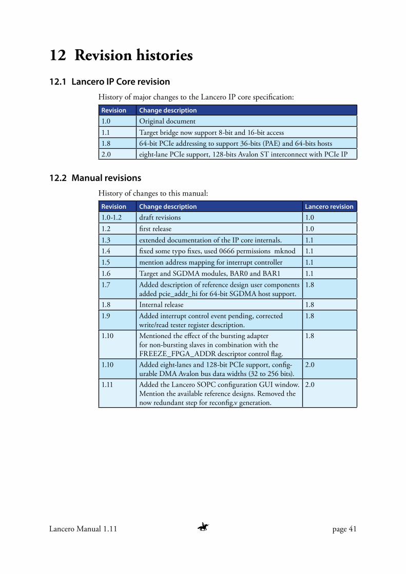
Revision histories12 Lancero IP Core revision12.1
History of major changes to the Lancero IP core speci"cation:Revision Change description1.0 Original document1.1 Target bridge now support 8-bit and 16-bit access1.8 64-bit PCIe addressing to support 36-bits (PAE) and 64-bits hosts2.0 eight-lane PCIe support, 128-bits Avalon ST interconnect with PCIe IP
Manual revisions12.2 History of changes to this manual:
Revision Change description Lancero revision1.0-1.2 draft revisions 1.01.2 "rst release 1.01.3 extended documentation of the IP core internals. 1.11.4 "xed some typo "xes, used 0666 permissions mknod 1.11.5 mention address mapping for interrupt controller 1.11.6 Target and SGDMA modules, BAR0 and BAR1 1.11.7 Added description of reference design user components
added pcie_addr_hi for 64-bit SGDMA host support.1.8
1.8 Internal release 1.81.9 Added interrupt control event pending, corrected
write/read tester register description.1.8
1.10 Mentioned the e!ect of the bursting adapter for non-bursting slaves in combination with the FREEZE_FPGA_ADDR descriptor control %ag.
1.8
1.10 Added eight-lanes and 128-bit PCIe support, con"g-urable DMA Avalon bus data widths (32 to 256 bits).
2.0
1.11 Added the Lancero SOPC con"guration GUI window.Mention the available reference designs. Removed the now redundant step for recon"g.v generation.
2.0

page 42 Lancero Manual 1.11
Support13 Support13.1
For technical support, information requests and updates surf to: http://www.logicandmore.com/
or send an e-mail to [email protected].