last lecture today’s lecture reading (ch 6)
TRANSCRIPT
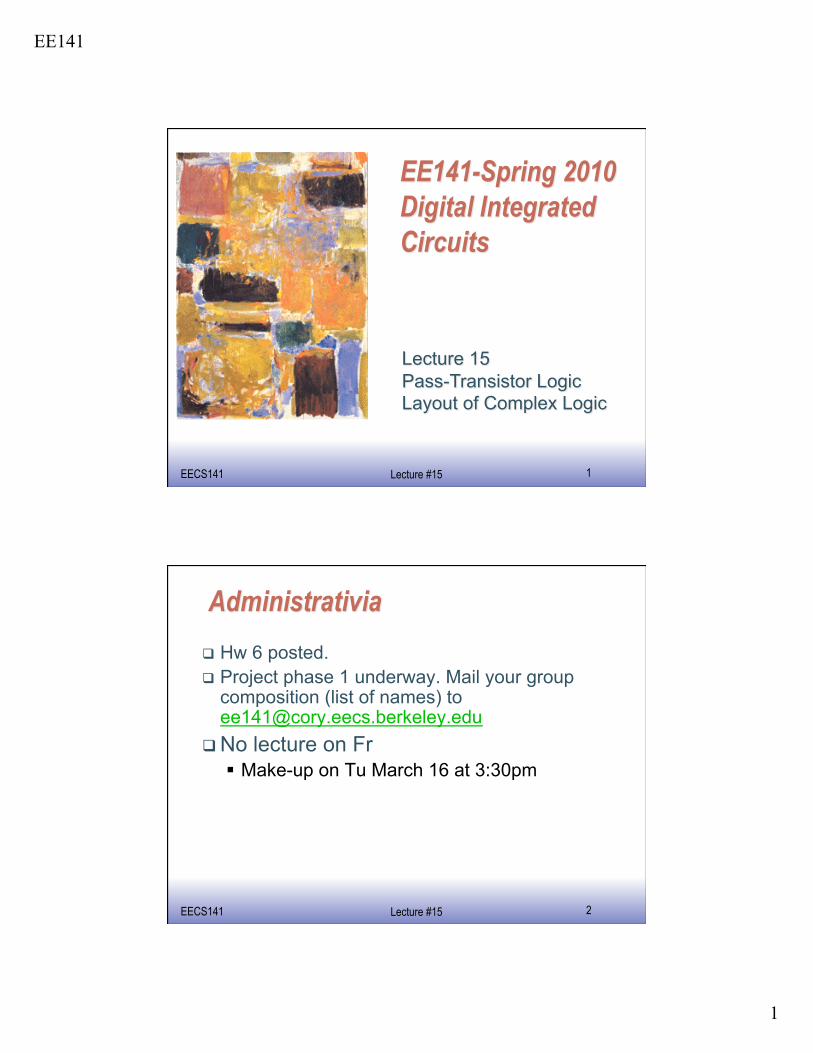
EE141
1
EE141 EECS141 1 Lecture #15
EE141 EECS141 2 Lecture #15
Hw 6 posted. Project phase 1 underway. Mail your group
composition (list of names) to [email protected]
No lecture on Fr Make-up on Tu March 16 at 3:30pm
EE141
2
EE141 EECS141 3 Lecture #15
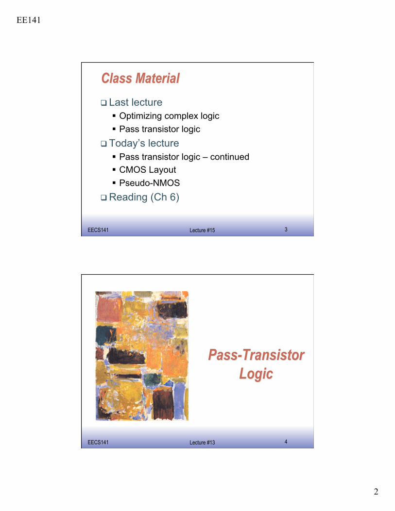
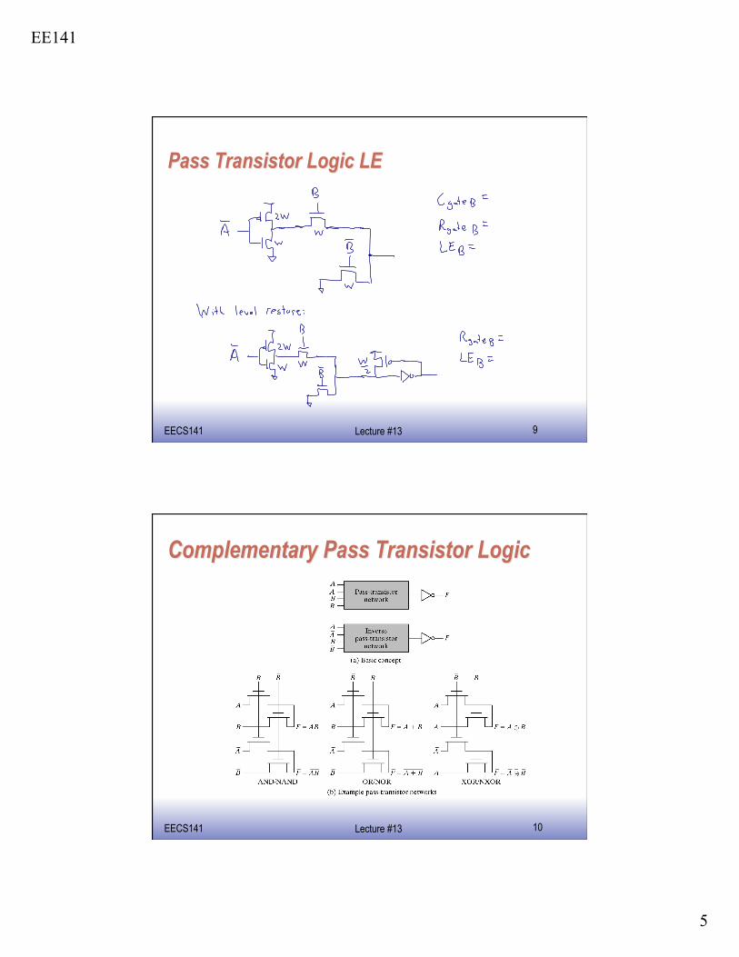
Last lecture Optimizing complex logic Pass transistor logic
Today’s lecture Pass transistor logic – continued CMOS Layout Pseudo-NMOS
Reading (Ch 6)
EE141 EECS141 4 Lecture #13
EE141
3
EE141 EECS141 5 Lecture #13
EE141 EECS141 6 Lecture #13
EE141
4
EE141 EECS141 7 Lecture #13
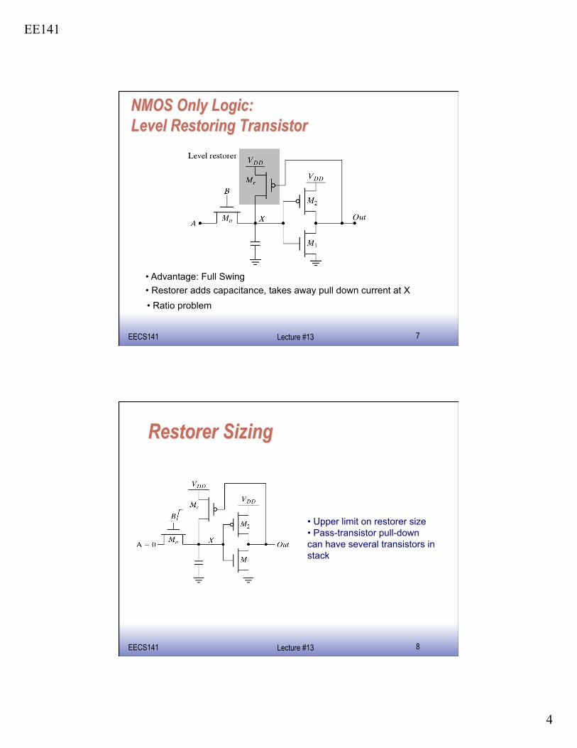
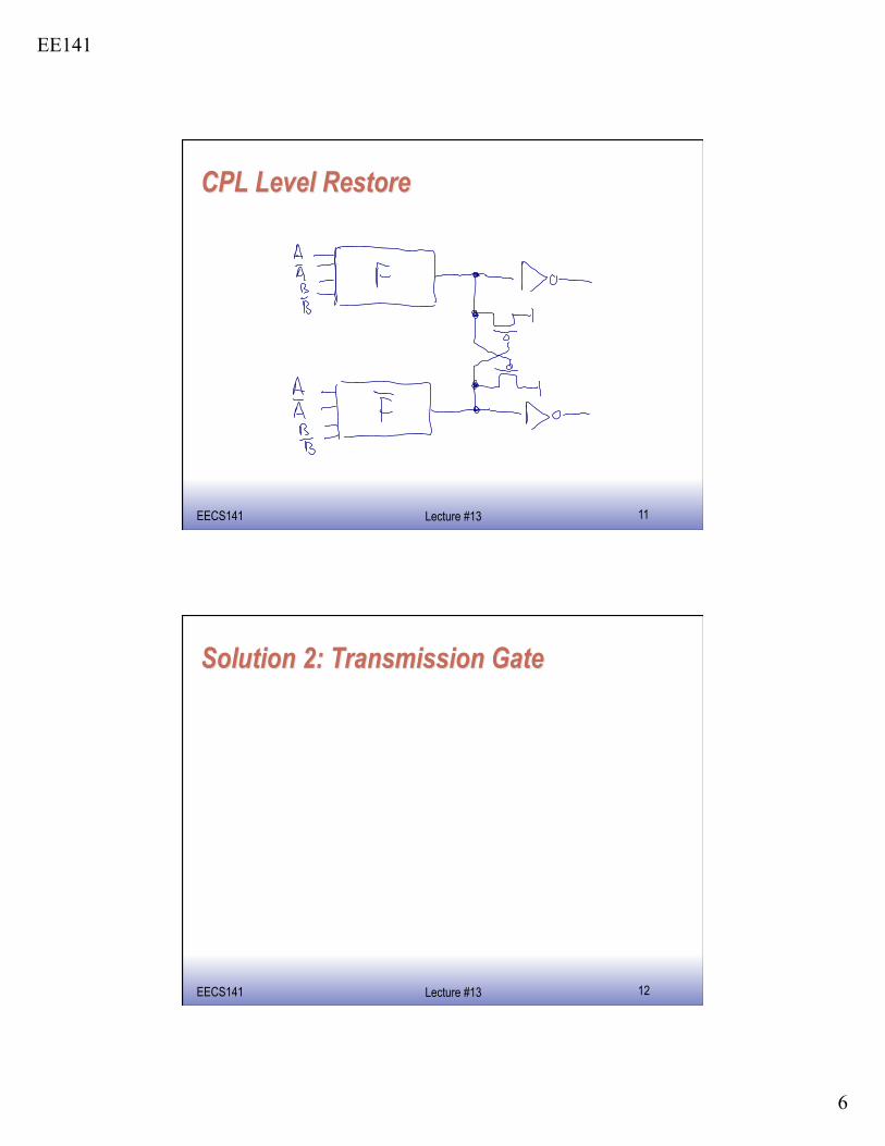
• Advantage: Full Swing • Restorer adds capacitance, takes away pull down current at X • Ratio problem
EE141 EECS141 8 Lecture #13
• Upper limit on restorer size • Pass-transistor pull-down can have several transistors in stack
EE141
5
EE141 EECS141 9 Lecture #13
EE141 EECS141 10 Lecture #13
EE141
6
EE141 EECS141 11 Lecture #13
EE141 EECS141 12 Lecture #13
EE141
7
EE141 EECS141 13 Lecture #13
EE141 EECS141 14 Lecture #13
EE141
8
EE141 EECS141 15 Lecture #13
EE141 EECS141 16 Lecture #13
EE141
9
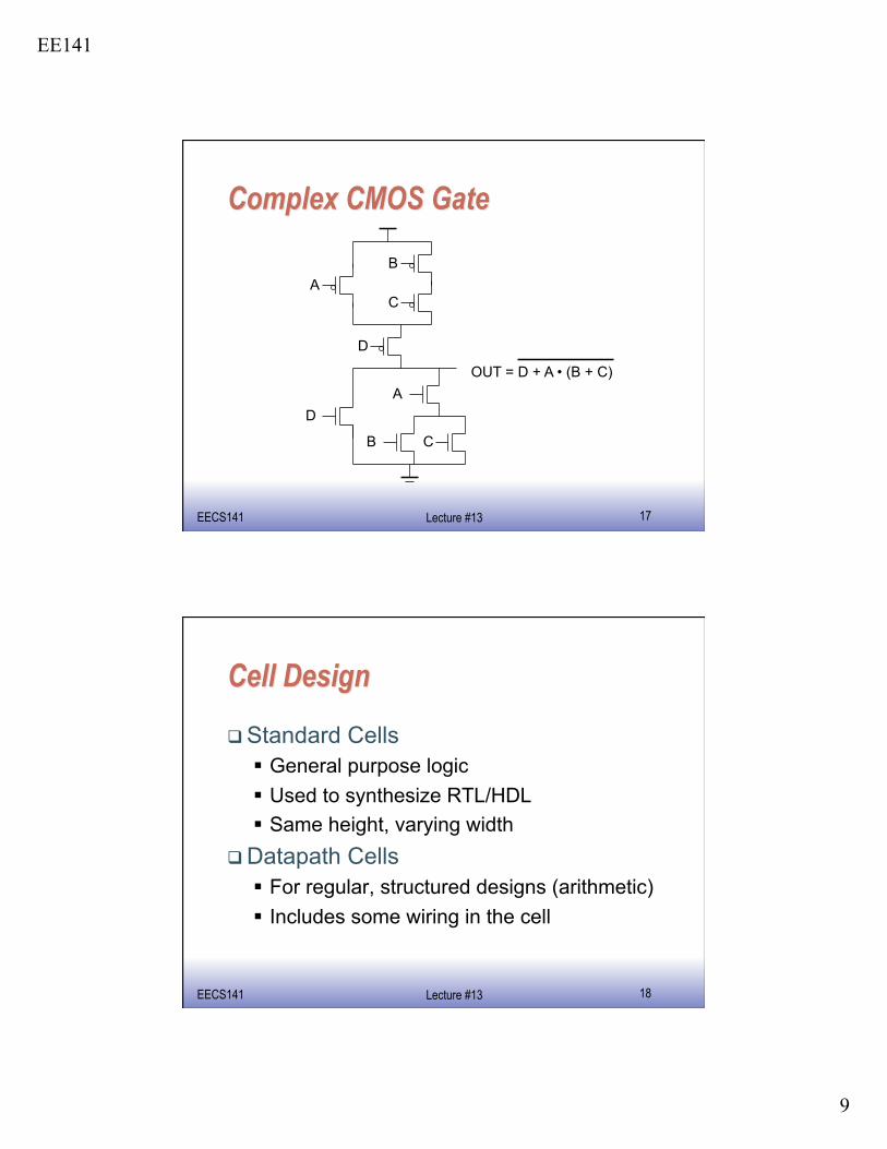
EE141 EECS141 17 Lecture #13
OUT = D + A • (B + C)
D A
B C
D
A B
C
EE141 EECS141 18 Lecture #13
Standard Cells General purpose logic Used to synthesize RTL/HDL Same height, varying width
Datapath Cells For regular, structured designs (arithmetic) Includes some wiring in the cell

EE141
10
EE141 EECS141 19 Lecture #13
EE141 EECS141 20 Lecture #13
EE141
11
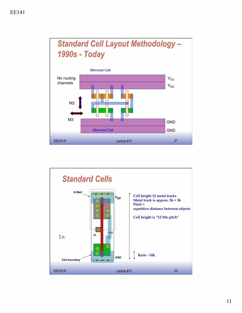
EE141 EECS141 21 Lecture #13
M2
No routing channels VDD
GND M3
VDD
GND
Mirrored Cell
Mirrored Cell
EE141 EECS141 22 Lecture #13
Cell boundary
N Well Cell height 12 metal tracks Metal track is approx. 3λ + 3λ Pitch = repetitive distance between objects
Cell height is “12 Mn pitch”
2λ
Rails ~10λ
In Out
V DD
GND
EE141
12
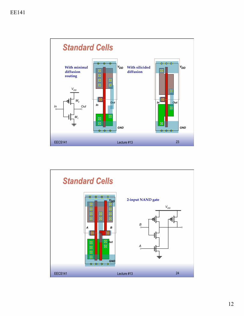
EE141 EECS141 23 Lecture #13
In Out
V DD
GND
In Out
V DD
GND
With silicided diffusion
With minimal diffusion routing
EE141 EECS141 24 Lecture #13
A
Out
V DD
GND
B
2-input NAND gate
EE141
13
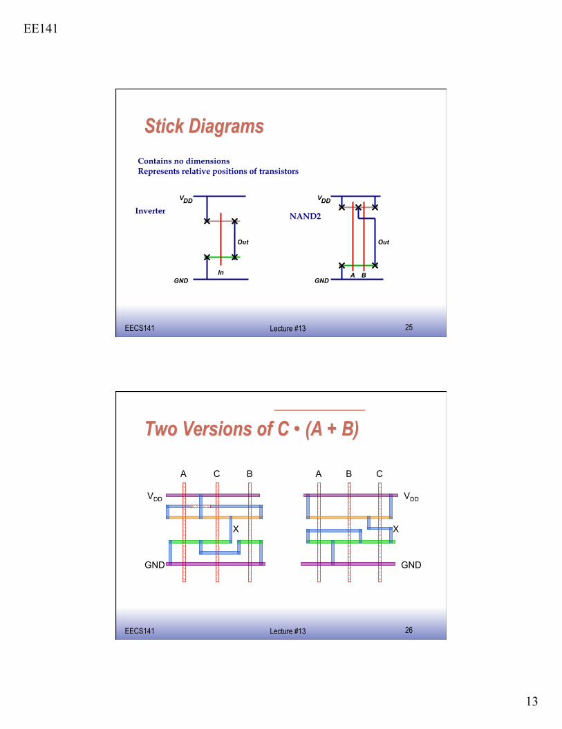
EE141 EECS141 25 Lecture #13
Contains no dimensions Represents relative positions of transistors
In
Out
V DD
GND
Inverter
A
Out
V DD
GND B
NAND2
EE141 EECS141 26 Lecture #13
X
C A B A B C
X
VDD
GND
VDD
GND
EE141
14
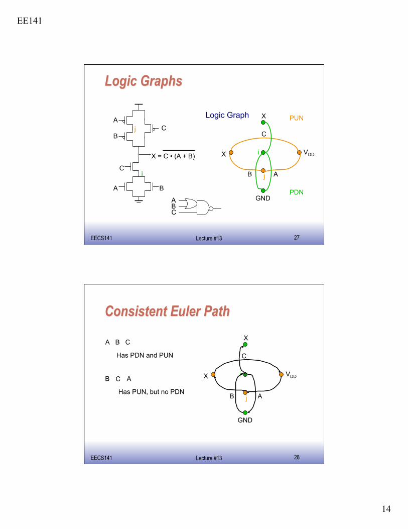
EE141 EECS141 27 Lecture #13
C
A B
X = C • (A + B)
B
A C
i j
VDD X
X
i
GND
A B
C
PUN
PDN A B C
Logic Graph j
EE141 EECS141 28 Lecture #13
j
VDD X
X
i
GND
A B
C
A B C
Has PDN and PUN
A B C
Has PUN, but no PDN
EE141
15
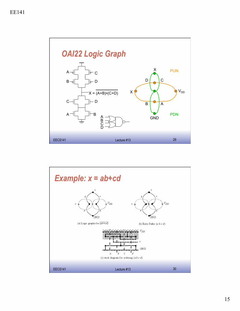
EE141 EECS141 29 Lecture #13
C
A B
X = (A+B)•(C+D)
B
A
D
VDD X
X
GND
A B
C
PUN
PDN
C
D
D
A B C D
EE141 EECS141 30 Lecture #13
EE141
16
EE141 EECS141 31 Lecture #13
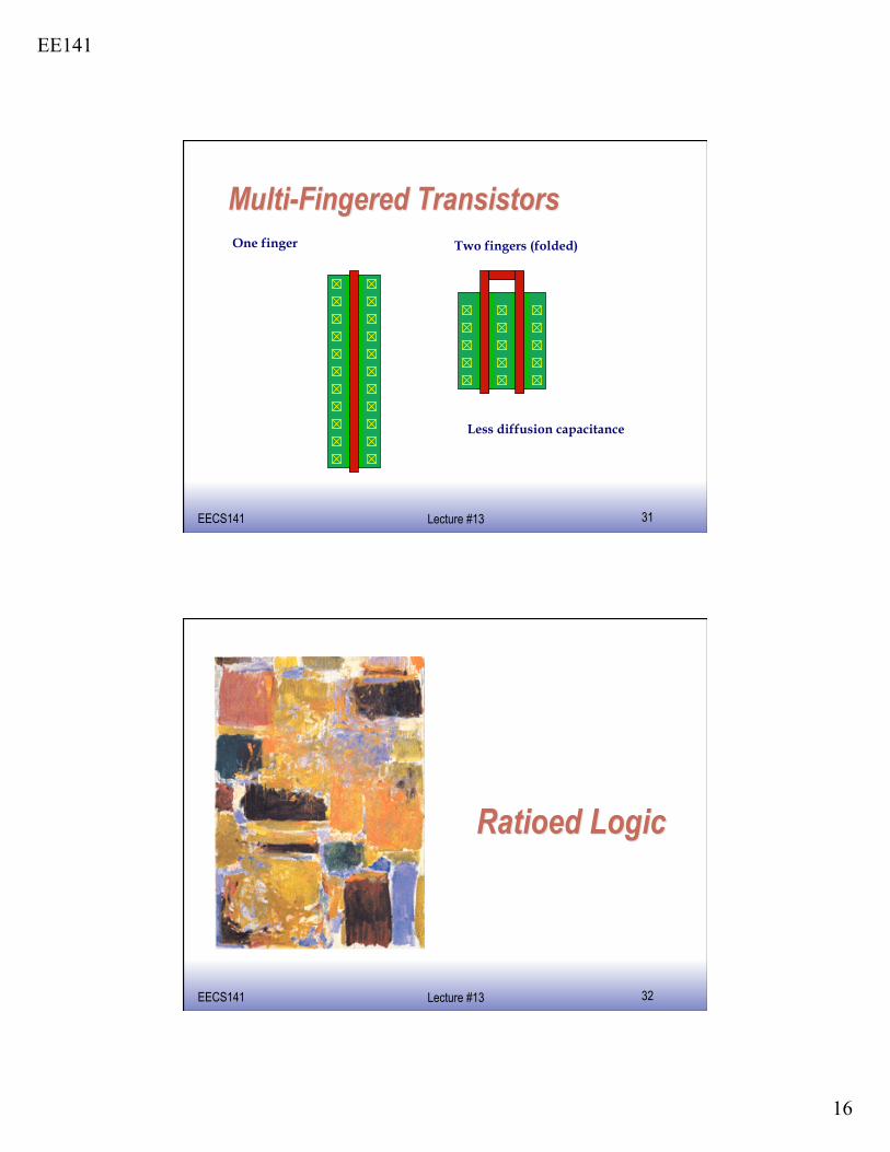
One finger Two fingers (folded)
Less diffusion capacitance
EE141 EECS141 32 Lecture #13
EE141
17
EE141 EECS141 33 Lecture #13
Goal: build gates faster/smaller than static complementary CMOS
EE141 EECS141 34 Lecture #13
Rising and falling delays aren’t the same Calculate LE for the two edges separately
For tpLH: Cgate = WCG Cinv = (3/2)WCG LELH =
EE141
18
EE141 EECS141 35 Lecture #13
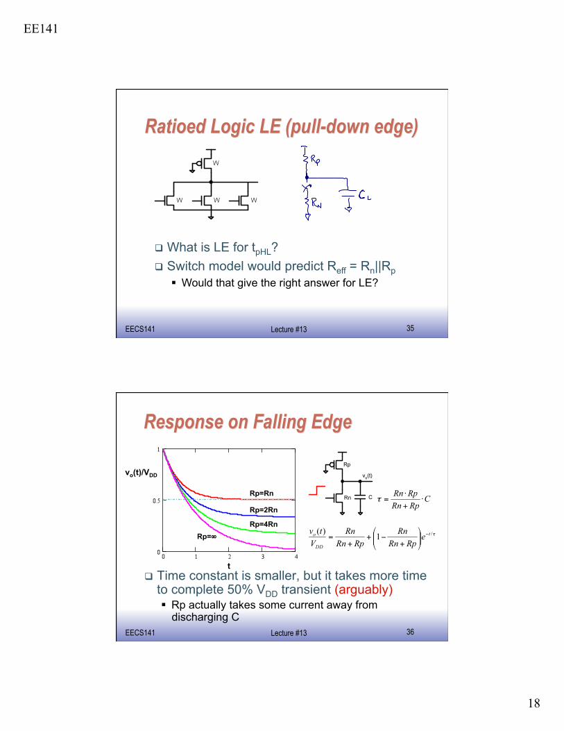
What is LE for tpHL? Switch model would predict Reff = Rn||Rp
Would that give the right answer for LE?
EE141 EECS141 36 Lecture #13
Time constant is smaller, but it takes more time to complete 50% VDD transient (arguably) Rp actually takes some current away from
discharging C
vo(t)/VDD
t
Rp=Rn
Rp=2Rn
Rp=4Rn
Rp=∞
EE141
19
EE141 EECS141 37 Lecture #13
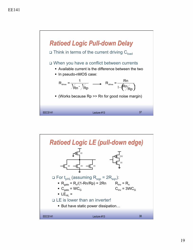
Think in terms of the current driving Cload
When you have a conflict between currents Available current is the difference between the two
In pseudo-nMOS case:
(Works because Rp >> Rn for good noise margin)
EE141 EECS141 38 Lecture #13
For tpHL (assuming Rsqp = 2Rsqn): Rgate = Rn/(1-Rn/Rp) = 2Rn Rinv = Rn
Cgate = WCG Cinv = 3WCG
LEHL = LE is lower than an inverter!
But have static power dissipation…
EE141
20
EE141 EECS141 39 Lecture #13
EE141 EECS141 40 Lecture #13
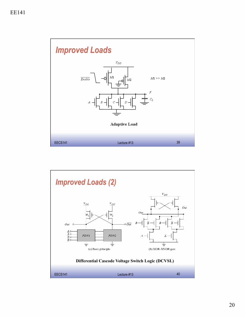
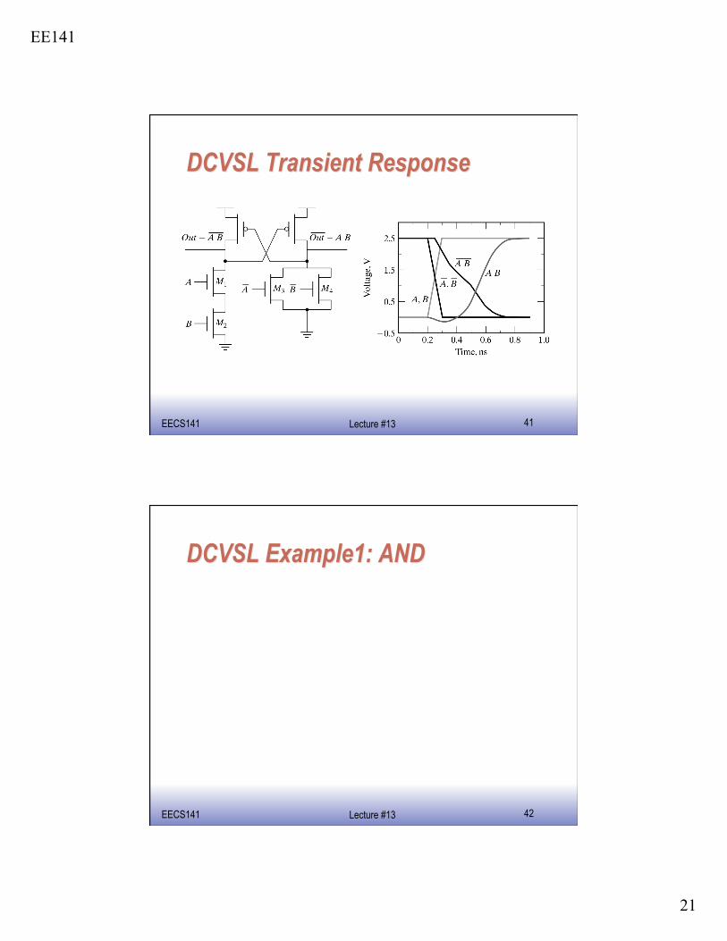
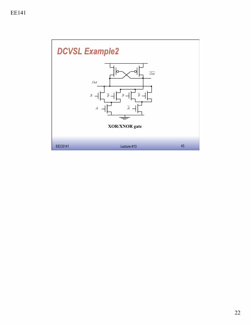
Differential Cascode Voltage Switch Logic (DCVSL)
EE141
21
EE141 EECS141 41 Lecture #13
EE141 EECS141 42 Lecture #13
EE141
22
EE141 EECS141 43 Lecture #13
XOR/XNOR gate