lecture 03 two port networks
DESCRIPTION
Two Port NetworksTRANSCRIPT
EEE 51: Second Semester 2014 -‐ 2015 Lecture 3
Two-‐Port Networks Single-‐Stage Amplifiers
EEEI -‐ University of the Philippines Diliman

Today
• Two-‐Port Networks • Single-‐Stage Amplifiers
EEEI -‐ University of the Philippines Diliman

Two-‐Port Network ReducEon
• Can reduce any linear circuit into 4 parameters
EEEI -‐ University of the Philippines Diliman
Linear à R, L, C, dependent sources
V1+−
+−V2
I1 I2
V1+−
I1
+−V2
I2
2-‐Port Network
Given 2 terminal parameters (V or I), we can get the other 2 (V or I)
I1I2
!
"##
$
%&&=
y11 y12y21 y22
!
"##
$
%&&
V1V2
!
"##
$
%&&
V1V2
!
"##
$
%&&=
z11 z12z21 z22
!
"##
$
%&&
I1I2
!
"##
$
%&&
V1I1
!
"##
$
%&&= A B
C D
!
"#
$
%&
V2−I2
!
"##
$
%&&
V1I2
!
"##
$
%&&=
h11 h12h21 h22
!
"##
$
%&&
I1V2
!
"##
$
%&&How convenient are
these representaEons for EEE 51?
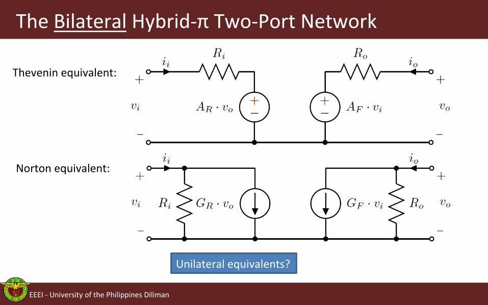
The Bilateral Hybrid-‐π Two-‐Port Network
EEEI -‐ University of the Philippines Diliman
Thevenin equivalent:
Norton equivalent:
Unilateral equivalents?
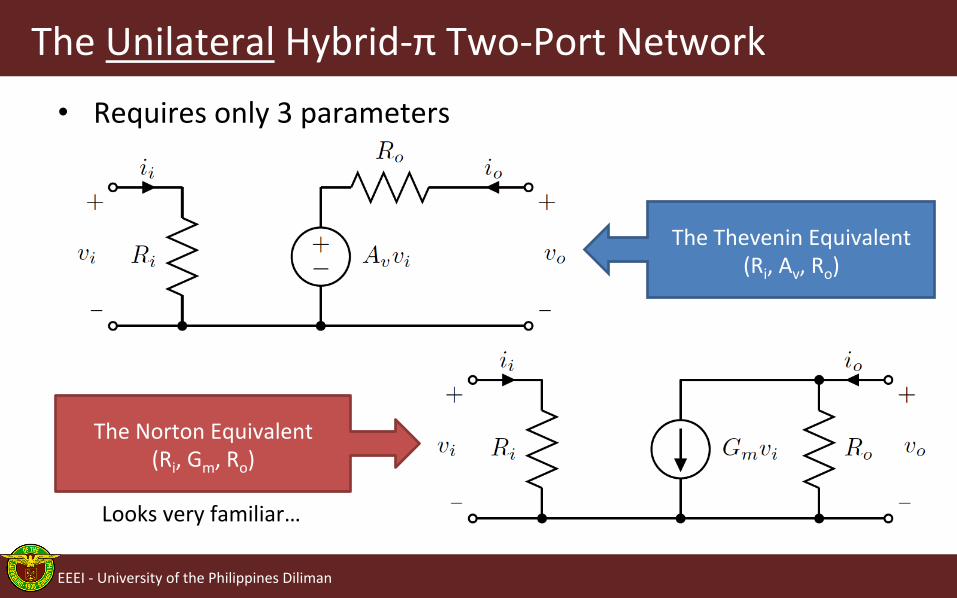
The Unilateral Hybrid-‐π Two-‐Port Network
• Requires only 3 parameters
EEEI -‐ University of the Philippines Diliman
The Thevenin Equivalent (Ri, Av, Ro)
The Norton Equivalent (Ri, Gm, Ro)
Looks very familiar…

OperaEng CondiEons (1)
• No-‐Load à No power draw at the output
EEEI -‐ University of the Philippines Diliman
Open circuit
Short circuit vo = 0
io = 0
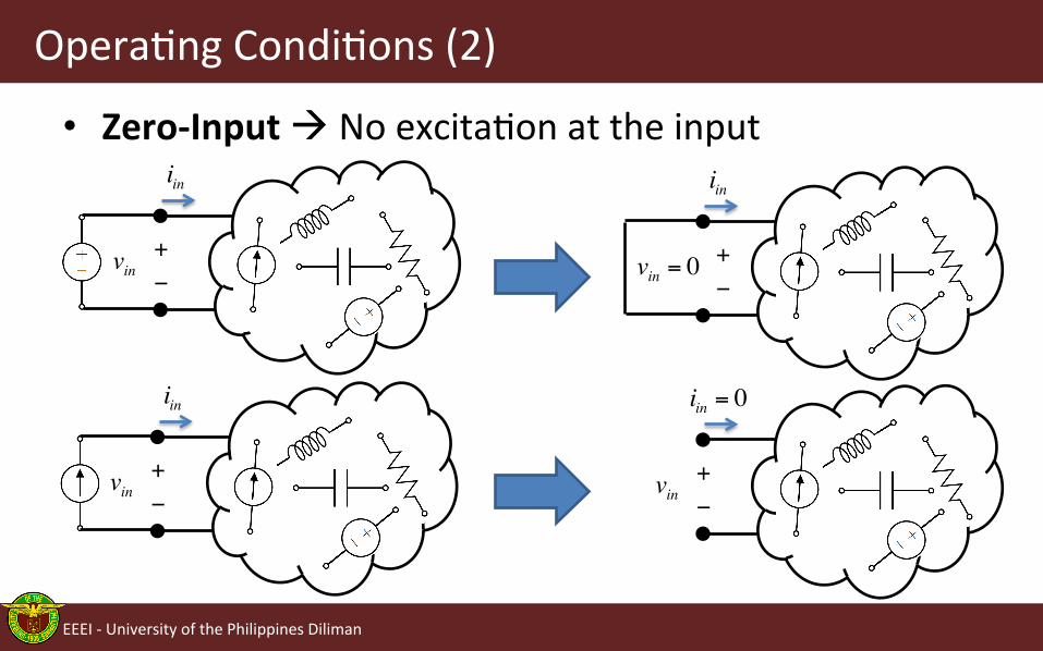
OperaEng CondiEons (2)
• Zero-‐Input à No excitaEon at the input
EEEI -‐ University of the Philippines Diliman
vin+−
iin
vin = 0+−
iin
vin+−
iin = 0
vin+−
iin
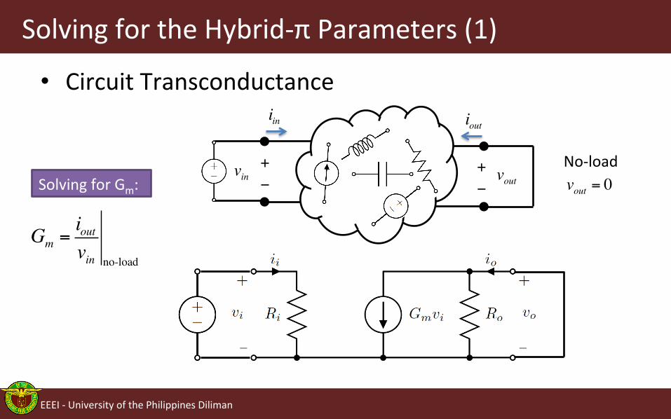
Solving for the Hybrid-‐π Parameters (1)
• Circuit Transconductance
EEEI -‐ University of the Philippines Diliman
Solving for Gm: vin
+−
+−vout
iin iout
No-‐load vout = 0
Gm =ioutvin no-load

Solving for the Hybrid-‐π Parameters (2)
• Circuit Voltage Gain
EEEI -‐ University of the Philippines Diliman
Solving for Av: vin
+−
+−vout
iin iout
No-‐load iout = 0
Av =voutvin no-load
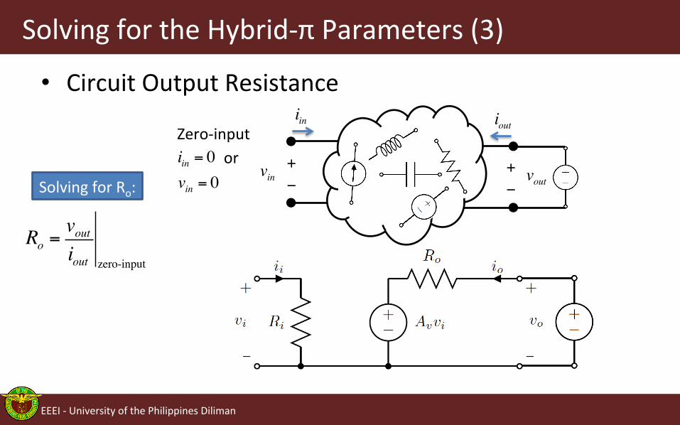
Solving for the Hybrid-‐π Parameters (3)
• Circuit Output Resistance
EEEI -‐ University of the Philippines Diliman
Solving for Ro: vin
+−
+−vout
iin ioutZero-‐input iin = 0vin = 0
Ro =voutiout zero-input
or
Solving for the Hybrid-‐π Parameters (4)
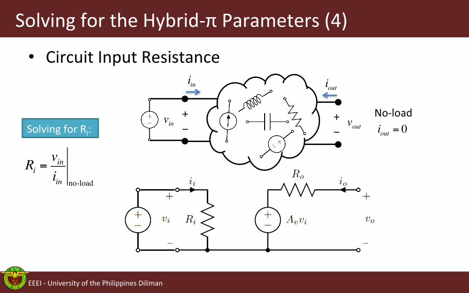
• Circuit Input Resistance
EEEI -‐ University of the Philippines Diliman
Solving for Ri: vin
+−
+−vout
iin iout
No-‐load iout = 0
Ri =viniin no-load
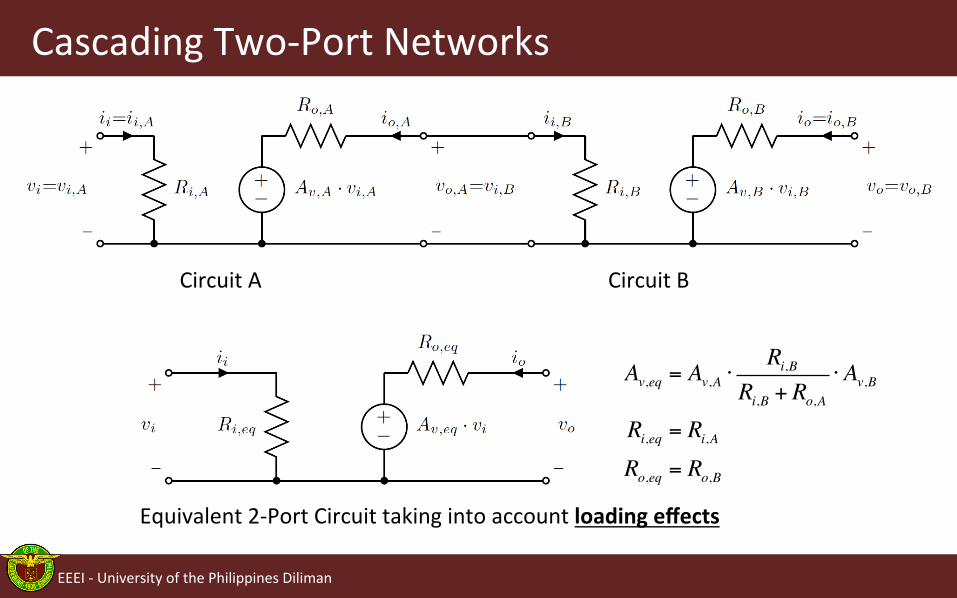
Cascading Two-‐Port Networks
EEEI -‐ University of the Philippines Diliman
Circuit A Circuit B
Equivalent 2-‐Port Circuit taking into account loading effects
Av,eq = Av,A ⋅Ri,B
Ri,B + Ro,A⋅Av,B
Ri,eq = Ri,ARo,eq = Ro,B

So Far… • We can analyze small signals
separately from large signals
• We can use 2-‐port networks to reduce/combine small signal circuits
• Let’s look at the small signal behavior of our basic electronic circuit building blocks: – Single-‐stage amplifiers
EEEI -‐ University of the Philippines Diliman
C
E
B D
S
G
Where do we put in the input?
Where do we get the output?
Choices:
Where do we start?
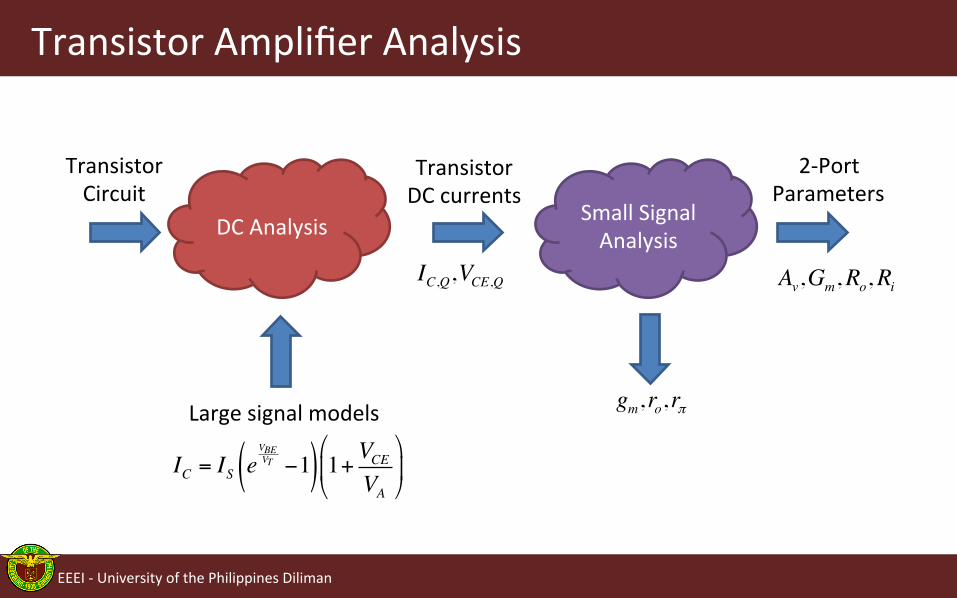
Transistor Amplifier Analysis
EEEI -‐ University of the Philippines Diliman
DC Analysis
Transistor Circuit
Small Signal Analysis
Transistor DC currents
Large signal models
2-‐Port Parameters
IC = IS eVBEVT −1( ) 1+VCEVA
"
#$
%
&'
IC,Q,VCE,Q
gm, ro, rπ
Av,Gm,Ro,Ri
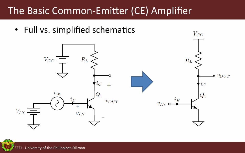
The Basic Common-‐Emi`er (CE) Amplifier
• Full vs. simplified schemaEcs
EEEI -‐ University of the Philippines Diliman
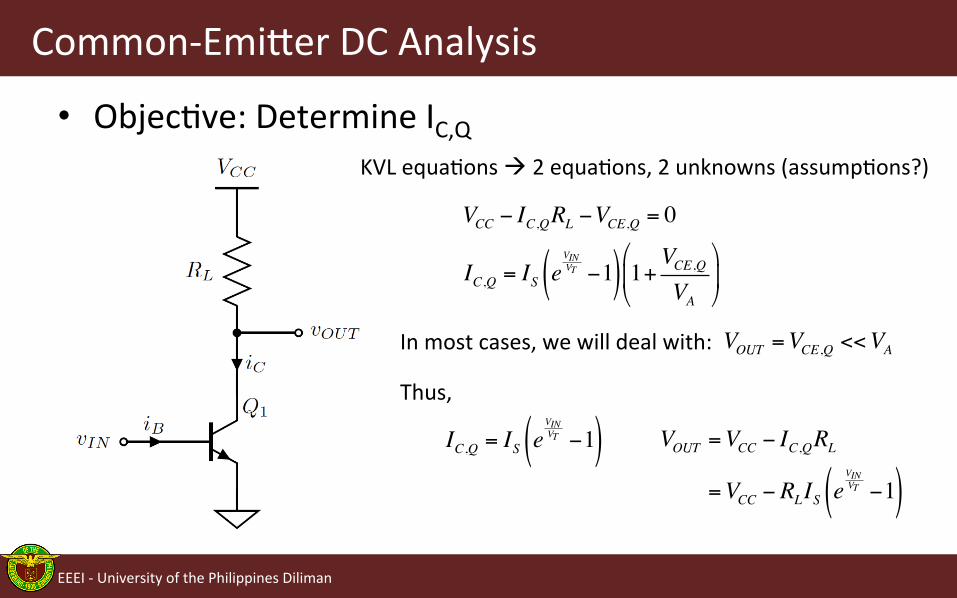
Common-‐Emi`er DC Analysis
• ObjecEve: Determine IC,Q
EEEI -‐ University of the Philippines Diliman
VCC − IC,QRL −VCE,Q = 0
IC,Q = IS eVINVT −1( ) 1+VCE,QVA
"
#$
%
&'
KVL equaEons à 2 equaEons, 2 unknowns (assumpEons?)
In most cases, we will deal with: VOUT =VCE,Q <<VA
IC,Q = IS eVINVT −1( )
Thus,
VOUT =VCC − IC,QRL
=VCC − RLIS eVINVT −1( )
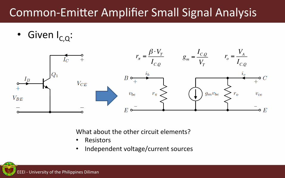
Common-‐Emi`er Amplifier Small Signal Analysis
• Given IC,Q:
EEEI -‐ University of the Philippines Diliman
ro =VAIC,Q
gm =IC,QVT
rπ =β ⋅VTIC,Q
What about the other circuit elements? • Resistors • Independent voltage/current sources

Linear Two-‐Terminal Devices
• Small signal conductance / resistance:
EEEI -‐ University of the Philippines Diliman
R VDC IDC
Rsmall signal =∂V∂I
V
I
IDC
V VDC
V
I I
Slope=1/R
Rsmall signal = R Rsmall signal = 0 Rsmall signal →∞
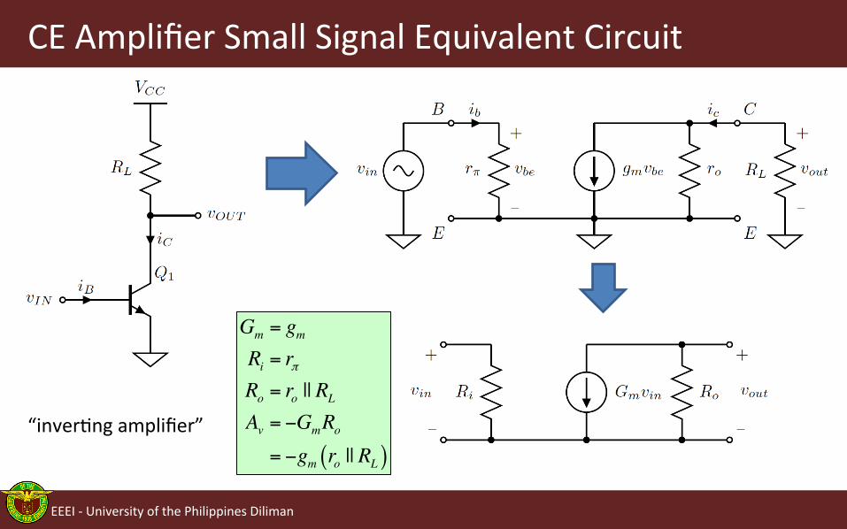
CE Amplifier Small Signal Equivalent Circuit
EEEI -‐ University of the Philippines Diliman
Gm = gmRi = rπRo = ro || RLAv = −GmRo= −gm ro || RL( )
“inverEng amplifier”
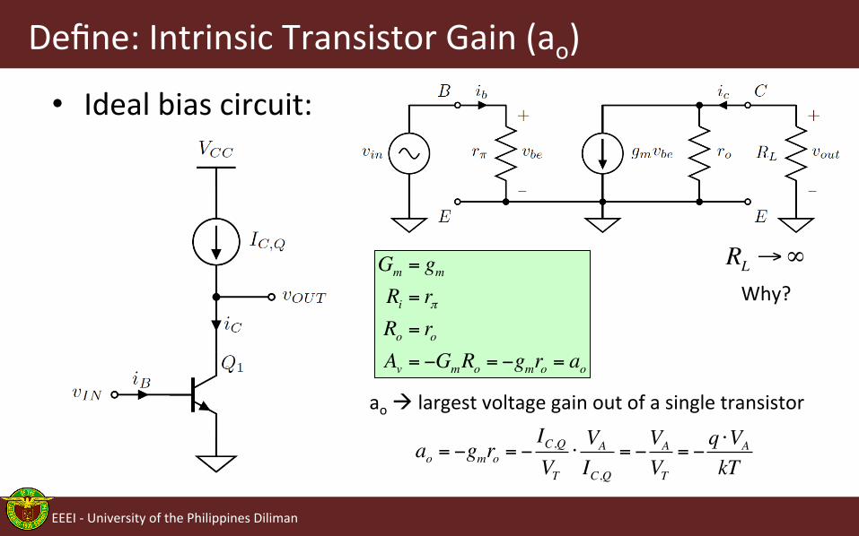
Define: Intrinsic Transistor Gain (ao)
• Ideal bias circuit:
EEEI -‐ University of the Philippines Diliman
Gm = gmRi = rπRo = roAv = −GmRo = −gmro = ao
ao à largest voltage gain out of a single transistor
RL →∞Why?
ao = −gmro = −IC,QVT
⋅VAIC,Q
= −VAVT
= −q ⋅VAkT
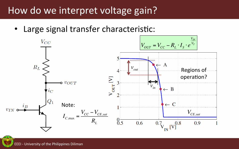
How do we interpret voltage gain?
• Large signal transfer characterisEc:
EEEI -‐ University of the Philippines Diliman
VOUT =VCC − RL ⋅ IS ⋅eVINVT
VCE,satNote:
IC,max =VCC −VCE,sat
RL
Regions of operaEon?
vin
vout
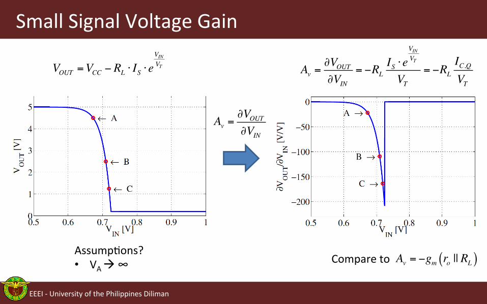
Small Signal Voltage Gain
EEEI -‐ University of the Philippines Diliman
Av =∂VOUT∂VIN
VOUT =VCC − RL ⋅ IS ⋅eVINVT Av =
∂VOUT∂VIN
= −RLIS ⋅e
VINVT
VT= −RL
IC,QVT
AssumpEons? • VA à ∞
Compare to Av = −gm ro || RL( )

Choosing the Bias Point?
• Largest gain? à Point C
EEEI -‐ University of the Philippines Diliman
VCC = 5VRL = 500Ω
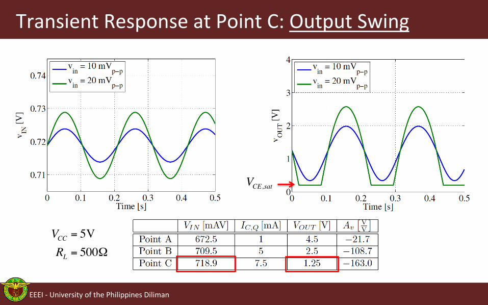
Transient Response at Point C: Output Swing
EEEI -‐ University of the Philippines Diliman
VCC = 5VRL = 500Ω
VCE,sat
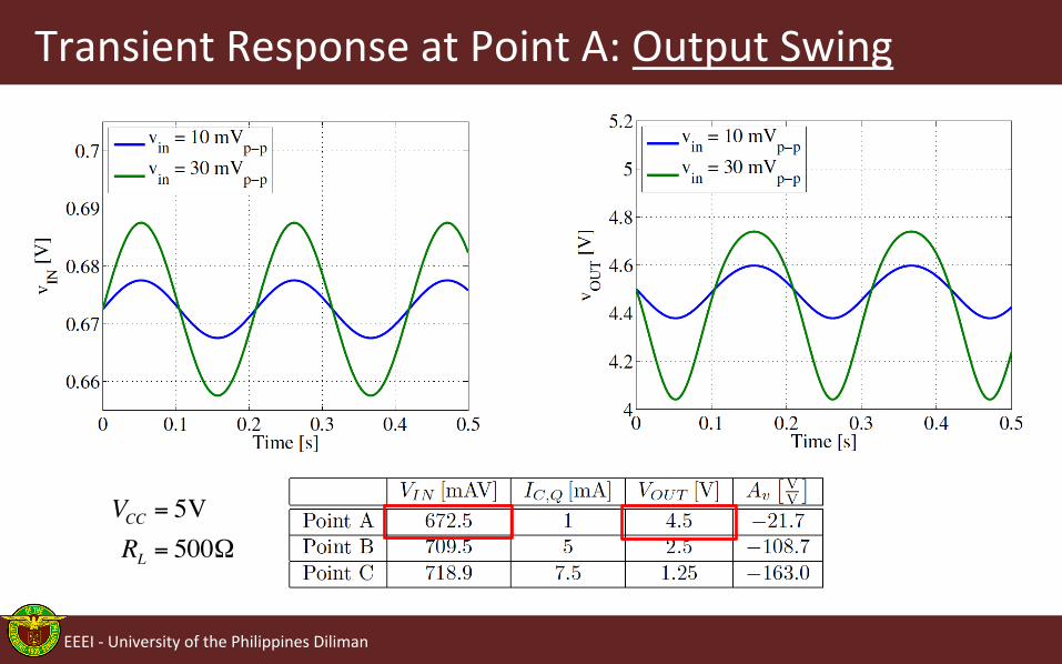
Transient Response at Point A: Output Swing
EEEI -‐ University of the Philippines Diliman
VCC = 5VRL = 500Ω
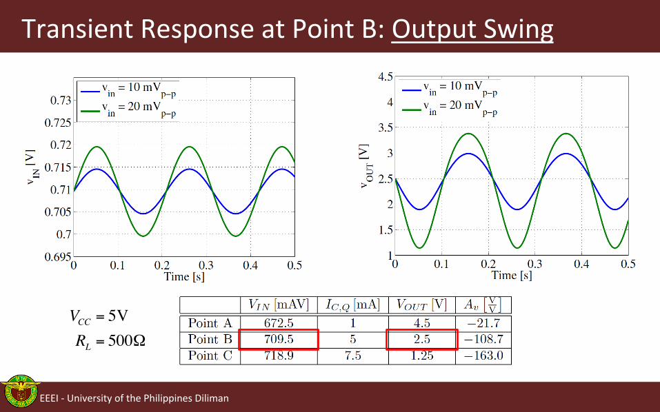
Transient Response at Point B: Output Swing
EEEI -‐ University of the Philippines Diliman
VCC = 5VRL = 500Ω
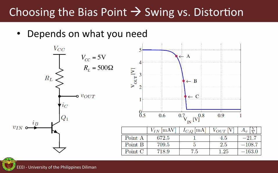
Choosing the Bias Point à Swing vs. DistorEon
• Depends on what you need
EEEI -‐ University of the Philippines Diliman
VCC = 5VRL = 500Ω
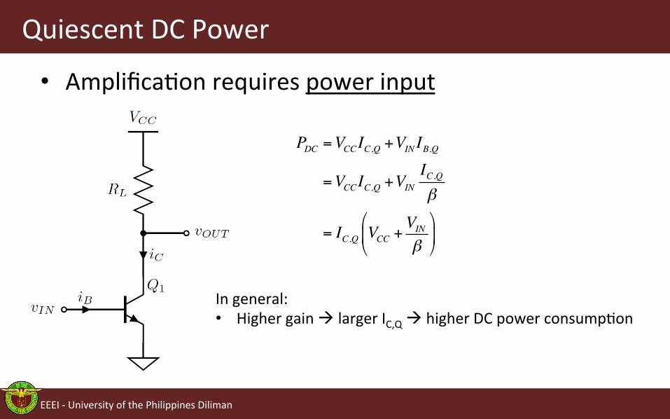
Quiescent DC Power
• AmplificaEon requires power input
EEEI -‐ University of the Philippines Diliman
PDC =VCCIC,Q +VIN IB,Q
=VCCIC,Q +VINIC,Qβ
= IC,Q VCC +VINβ
!
"#
$
%&
In general: • Higher gain à larger IC,Q à higher DC power consumpEon
Next MeeEng
• Single-‐Stage Amplifiers – Common-‐Emi`er Biasing – Common-‐Source Amplifier
– Common-‐Base / Common-‐Gate Amplifier
– Common-‐Collector / Common-‐Drain Amplifier
EEEI -‐ University of the Philippines Diliman