lecture 4: fundamentals of nucleation and growth;...
TRANSCRIPT
Lecture 4:
Fundamentals of Nucleation and Growth; Control of microstructure
evolution
A. Neugebauer, “Condensation, Nucleation, and Growth of Thin Films,” in Handbook of Thin Film Technology, edited by L.I. Maissel and R. Glang, McGraw-Hill, New York 1970.
J.E. Greene, “Physics of Film Growth from the Vapor Phase,” in Multicomponent and Multilayered Thin Films for Advanced Technologies: Techniques, Fundamentals, and Devices, ed. by O. Auciello, NATO Advanced Study Institute, KluwerAcademic Publishers, Boston 1993, p. 39.
J.A. Venables, Introduction to Surface and Thin Film Processes, Cambridge University Press, Cambridge, UK 2000.
K.H. Müller, Journal of Applied Physics. 58, 2573 (1985).
B. Mutaftschiev, The Atomistic Nature of Crystal Growth (Springer Press, New York, 2001).
J.L. Vossen and J.J. Cuomo, “Glow Discharge Sputter Deposition, “ in Thin Film Processes, edited by J.L. Vossen and W. Kern, Academic Press, NY 1978.
J.A. Thornton and A.S. Penfold, “Cylindrical Magnetron Sputtering,” in Thin Film Processes, edited by J.L. Vossen and W. Kern, Academic Press, NY 1978.
R.K. Waits, “Planar Magnetron Sputtering,” in Thin Film Processes, edited by J.L. Vossen and W. Kern, Academic Press, New York 1978.
B. Chapman, Glow Discharge Processes, Wiley Interscience, New York 1980.
J.A. Thornton and J.E. Greene, “Plasmas in Deposition Processes,” in Deposition Technologies for Films and Coatings, edited by R.F. Bunshah, Noayes Publications, Park Ridge, New Jersey 1994, p. 29.
S.M. Rossnagel, “Magnetron Plasma Deposition Processes,” in Handbook of Plasma Processing Technology, edited by S.M. Rossnagel, J.J. Cuomo, and W.D. Westwood Noyes Publications, Park Ridge, New Jersey 1990.
K.H. Müller, “Film Growth Modification by Concurrent Ion Bombardment: Theory and Simulation,” in Handbook of Ion-Beam Processing Technology, edited by J.J. Coumo, S.M. Rossnagel, and H.R. Kaufman, Noyes Publications, Park Ridge, New Jersey 1989, p. 241.
Bibliography
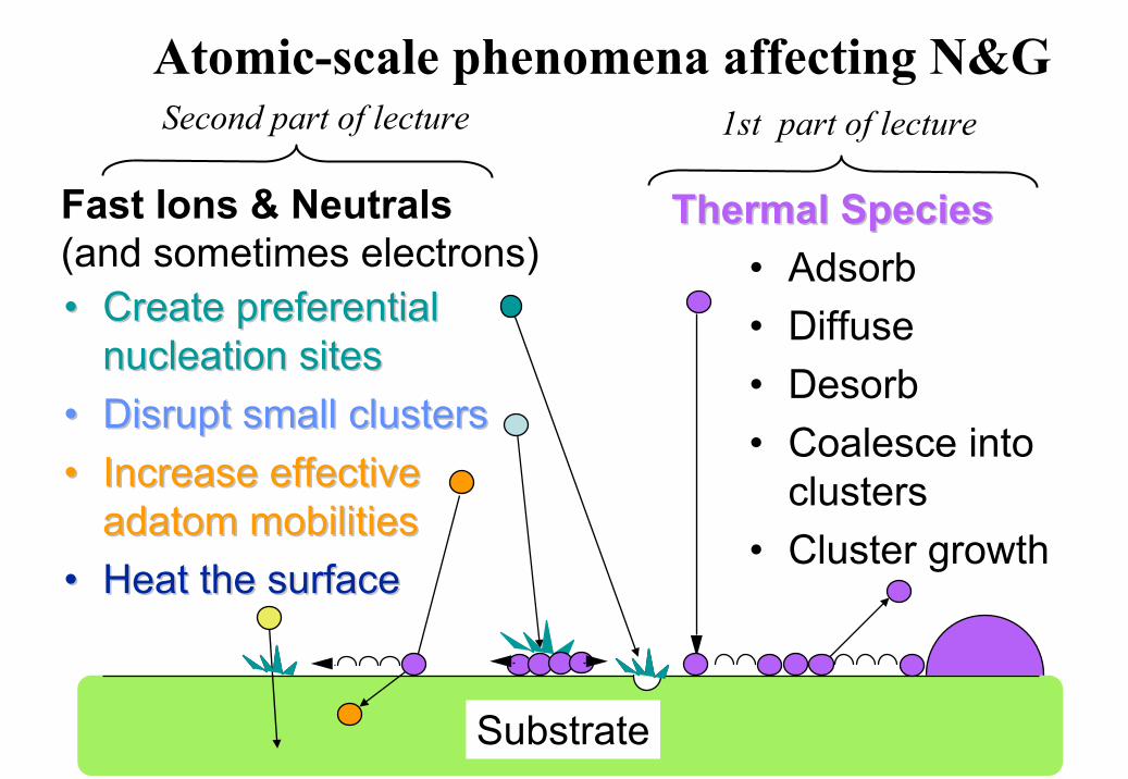
•• Create preferential Create preferential nucleation sitesnucleation sites
•• Disrupt small clustersDisrupt small clusters•• Increase effective Increase effective
adatom mobilitiesadatom mobilities•• Heat the surfaceHeat the surface
Substrate
Thermal SpeciesThermal SpeciesFast Ions & Neutrals (and sometimes electrons) • Adsorb
• Diffuse• Desorb• Coalesce into
clusters• Cluster growth
Atomic-scale phenomena affecting N&GSecond part of lecture 1st part of lecture
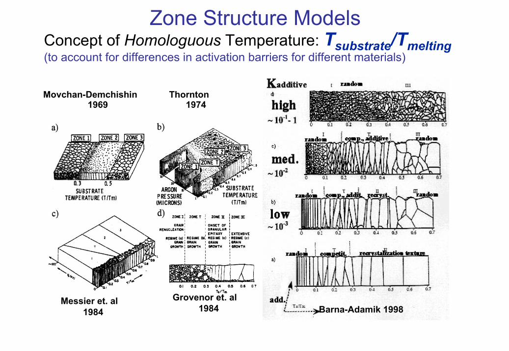
Movchan-Demchishin1969
Thornton1974
Messier et. al1984
Grovenor et. al1984 Barna-Adamik 1998
Zone Structure ModelsConcept of Homologuous Temperature: Tsubstrate/Tmelting(to account for differences in activation barriers for different materials)
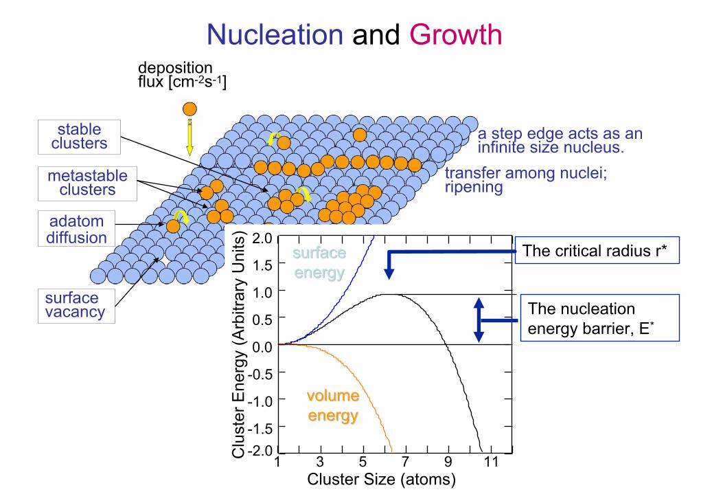
transfer among nuclei; ripening
deposition flux [cm-2s-1]
a step edge acts as an infinite size nucleus.
metastableclusters
surface vacancy
adatom diffusion
Nucleation and Growth
stableclusters
Cluster Size (atoms)
The critical radius r*
The nucleation energy barrier, E*
-2.0-1.5
-1.0
-0.5
0.0
0.5
1.0
1.5
2.0C
lust
er E
nerg
y (A
rbitr
ary
Uni
ts)
1 3 5 7 9 11
volume volume energyenergy
surface surface energyenergy
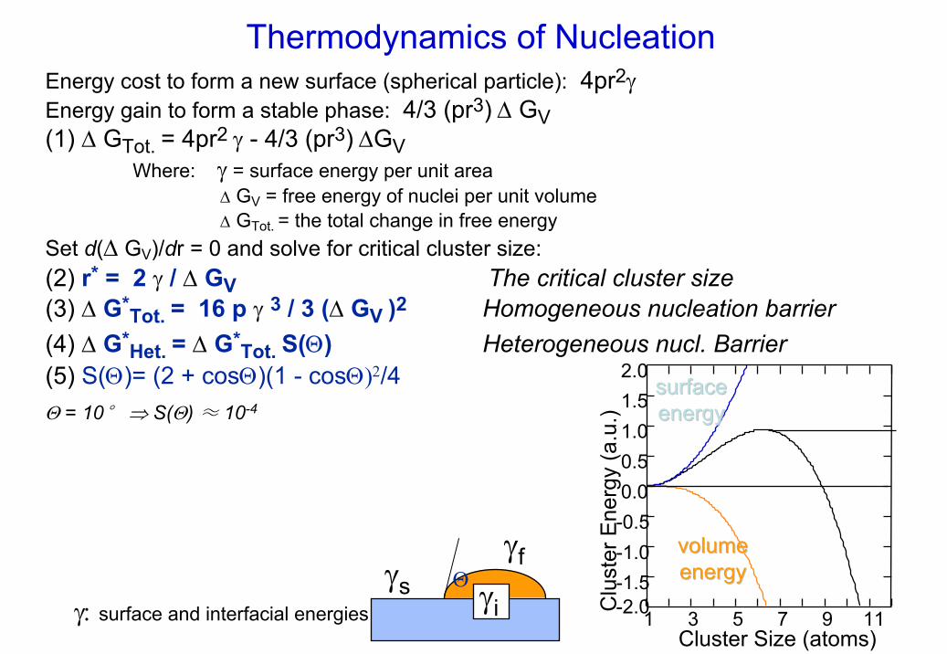
Thermodynamics of Nucleation
Cluster Size (atoms)-2.0-1.5-1.0-0.50.00.51.01.52.0
Clu
ster
Ene
rgy
(a.u
.)1 3 5 7 9 11
volume volume energyenergy
surface surface energyenergy
Energy cost to form a new surface (spherical particle): 4pr2γEnergy gain to form a stable phase: 4/3 (pr3) ∆ GV(1) ∆ GTot. = 4pr2 γ - 4/3 (pr3) ∆GV
Where: γ = surface energy per unit area∆ GV = free energy of nuclei per unit volume∆ GTot. = the total change in free energy
Set d(∆ GV)/dr = 0 and solve for critical cluster size:(2) r* = 2 γ / ∆ GV The critical cluster size(3) ∆ G*Tot. = 16 p γ 3 / 3 (∆ GV )2 Homogeneous nucleation barrier(4) ∆ G*Het. = ∆ G*Tot. S(Θ) Heterogeneous nucl. Barrier(5) S(Θ)= (2 + cosΘ)(1 - cosΘ)2/4Θ = 10° ⇒ S(Θ) ≈ 10-4
surface and interfacial energies
γs γi
γf
γ:Θ
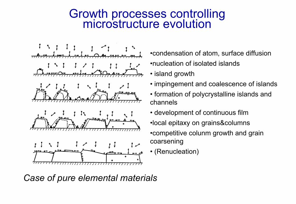
Growth processes controllingmicrostructure evolution
•condensation of atom, surface diffusion •nucleation of isolated islands• island growth• impingement and coalescence of islands• formation of polycrystalline islands and channels• development of continuous film•local epitaxy on grains&columns•competitive colunm growth and grain coarsening• (Renucleation)
Case of pure elemental materials
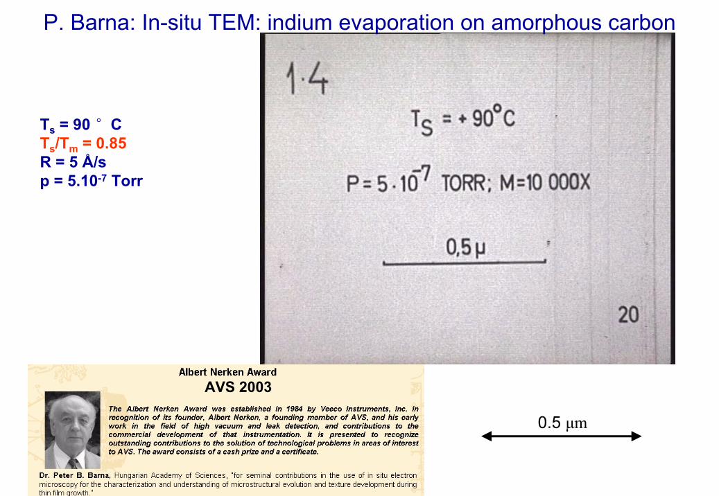
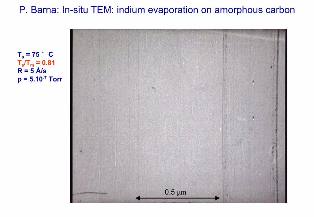
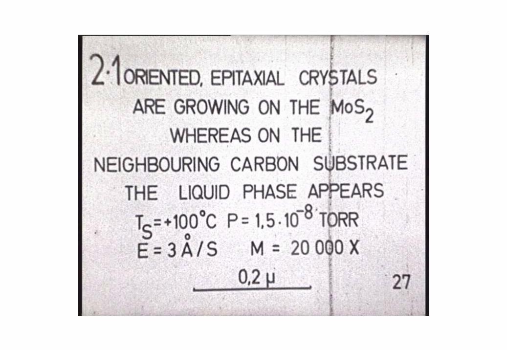
Ts = 90 °CTs/Tm = 0.85R = 5 Å/sp = 5.10-7 Torr
P. Barna: In-situ TEM: indium evaporation on amorphous carbon
0.5 µm
AVS 2003
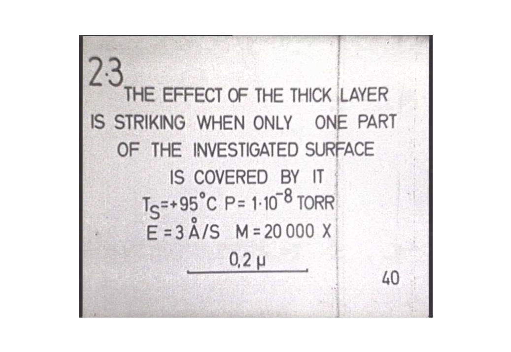
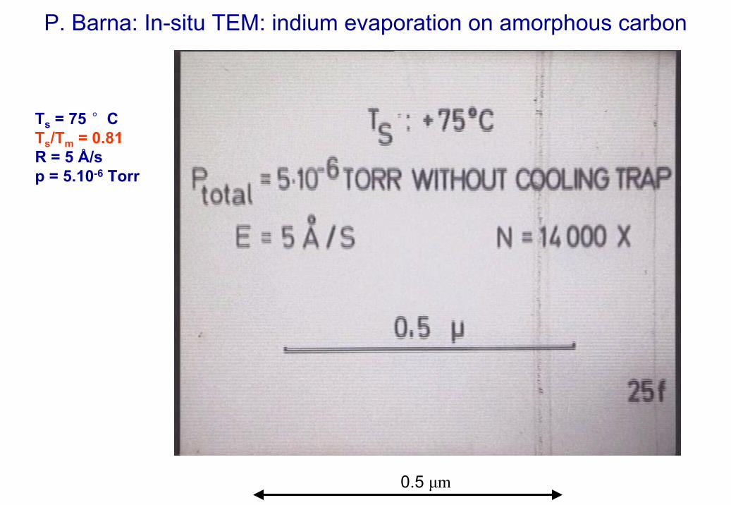
Ts = 75 °CTs/Tm = 0.81R = 5 Å/sp = 5.10-7 Torr
0.5 µm
P. Barna: In-situ TEM: indium evaporation on amorphous carbon
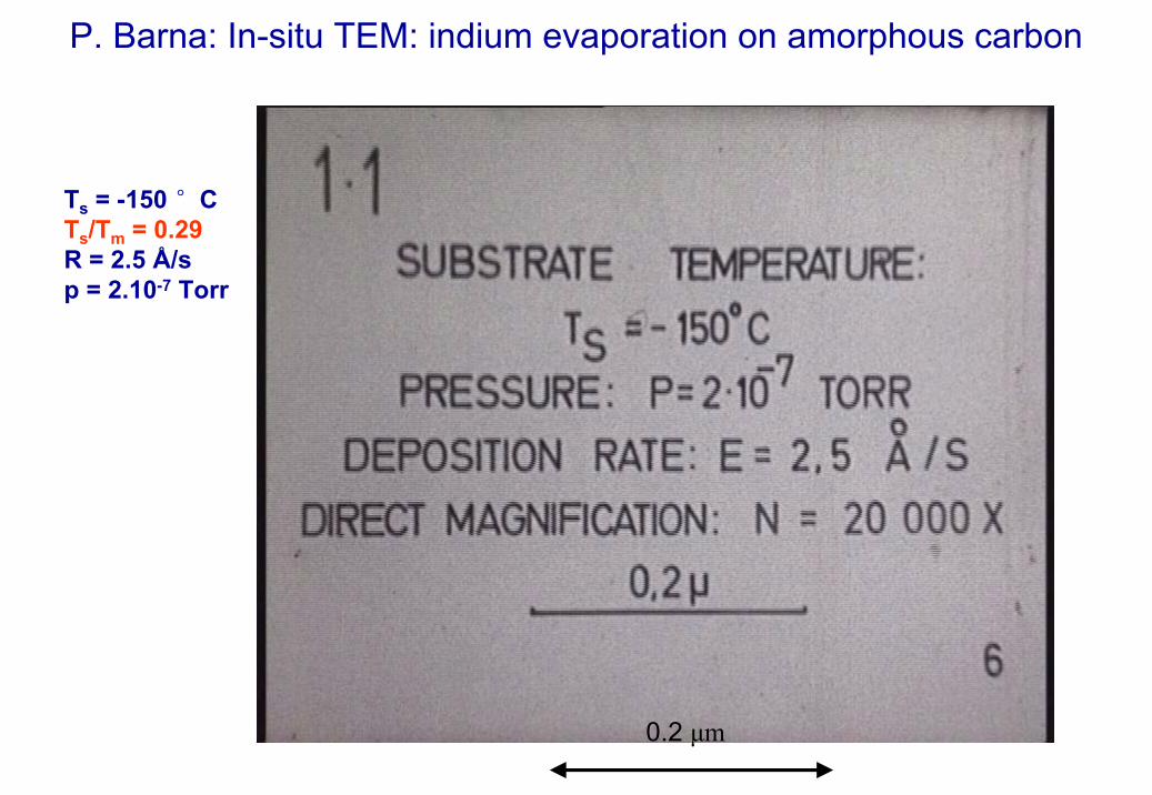
Ts = -150 °CTs/Tm = 0.29R = 2.5 Å/sp = 2.10-7 Torr
0.2 µm
P. Barna: In-situ TEM: indium evaporation on amorphous carbon
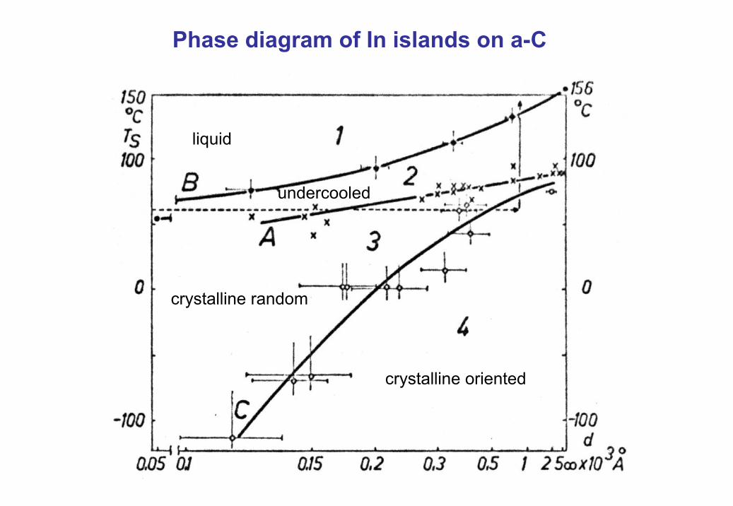
Phase diagram of In islands on a-C
liquid
crystalline random
crystalline oriented
undercooled

Growth processes controllingmicrostructure evolution
•condensation of atom, surface diffusion •nucleation of isolated islands• island growth• impingement and coalescence of islands• formation of polycrystalline islands and channels• development of continuous film•local epitaxy on grains&columns•competitive colunm growth and grain coarsening• (Renucleation)
Case of pure elemental materials
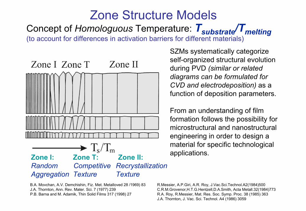
Zone I: Zone T: Zone II:Random Competitive RecrystallizationAggregation Texture TextureB.A. Movchan, A.V. Demchishin, Fiz. Met. Metalloved 28 /1969) 83J.A. Thornton, Ann. Rev. Mater. Sci. 7 (1977) 239P.B. Barna and M. Adamik, Thin Solid Films 317 (1998) 27
SZMs systematically categorize self-organized structural evolution during PVD (similar or related diagrams can be formulated for CVD and electrodeposition) as a function of deposition parameters.
From an understanding of film formation follows the possibility for microstructural and nanostructural engineering in order to design a material for specific technological applications.
R.Messier, A.P.Giri, A.R. Roy, J.Vac.Sci.Technol.A2(1984)500C.R.M.Grovenor,H.T.G.Hentzell,D.A.Smith, Acta Metall.32(1984)773R.A. Roy, R.Messier, Mat. Res. Soc. Symp. Proc. 38 (1985) 363J.A. Thornton, J. Vac. Sci. Technol. A4 (1986) 3059
Zone Structure ModelsConcept of Homologuous Temperature: Tsubstrate/Tmelting(to account for differences in activation barriers for different materials)
Ts = 75 °CTs/Tm = 0.81R = 5 Å/sp = 5.10-6 Torr
0.5 µm
P. Barna: In-situ TEM: indium evaporation on amorphous carbon
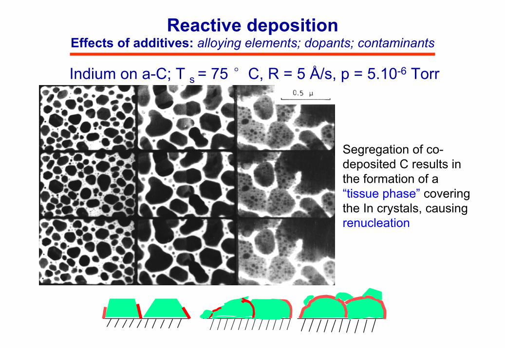
Segregation of co-deposited C results in the formation of a “tissue phase” covering the In crystals, causing renucleation
Reactive depositionEffects of additives: alloying elements; dopants; contaminants
Indium on a-C; T s = 75 °C, R = 5 Å/s, p = 5.10-6 Torr
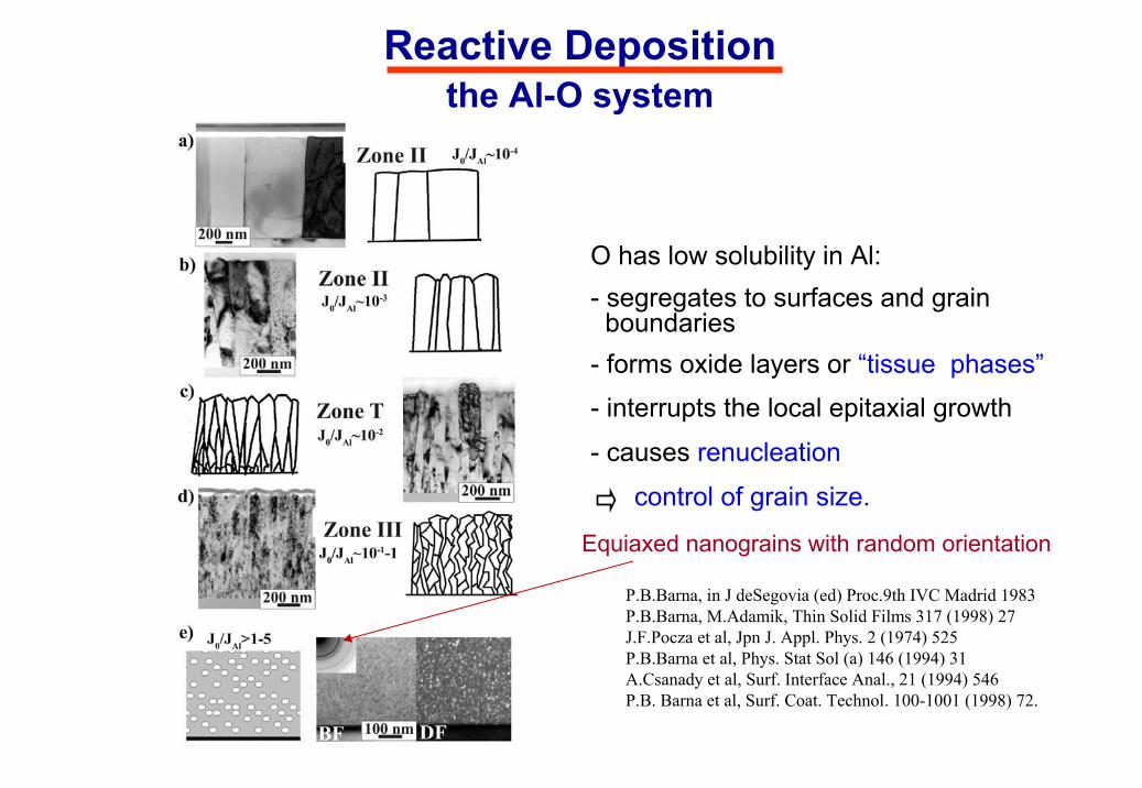
Reactive Depositionthe Al-O system
Equiaxed nanograins with random orientation
P.B.Barna, in J deSegovia (ed) Proc.9th IVC Madrid 1983P.B.Barna, M.Adamik, Thin Solid Films 317 (1998) 27J.F.Pocza et al, Jpn J. Appl. Phys. 2 (1974) 525P.B.Barna et al, Phys. Stat Sol (a) 146 (1994) 31A.Csanady et al, Surf. Interface Anal., 21 (1994) 546P.B. Barna et al, Surf. Coat. Technol. 100-1001 (1998) 72.
O has low solubility in Al:- segregates to surfaces and grainboundaries
- forms oxide layers or “tissue phases”- interrupts the local epitaxial growth
- causes renucleation
control of grain size.
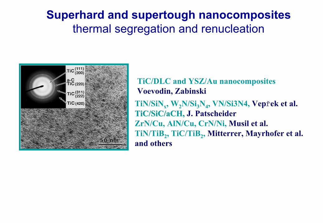
TiC/DLC and YSZ/Au nanocomposites Voevodin, Zabinski
Superhard and supertough nanocompositesthermal segregation and renucleation
TiN/SiNx, W2N/Si3N4, VN/Si3N4, Vepřek et al.TiC/SiC/aCH,TiC/SiC/aCH, J. PatscheiderZrN/Cu, AlN/Cu, CrN/Ni, Musil et al.TiN/TiB2, TiC/TiB2, Mitterrer, Mayrhofer et al.and others
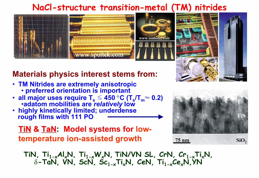
75 nm SiO2
TiN
NaCl-structure transition-metal (TM) nitrides
Materials physics interest stems from:• TM Nitrides are extremely anisotropic
• preferred orientation is important• all major uses require Ts ≤ 450 °C (Ts/Tm≈ 0.2)
•adatom mobilities are relatively low• highly kinetically limited; underdense
rough films with 111 PO
TiNTiN & & TaNTaN: Model systems for low-temperature ion-assisted growth
TiN, Ti1-xAlxN, Ti1-xWxN, TiN/VN SL, CrN, Cr1-xTixN, δ-TaN, VN, ScN, Sc1-xTixN, CeN, Ti1-xCexN,YN
www.provmet.comwww.provmet.com
www.sputtek.comwww.sputtek.com
www.ionbond.comwww.ionbond.com
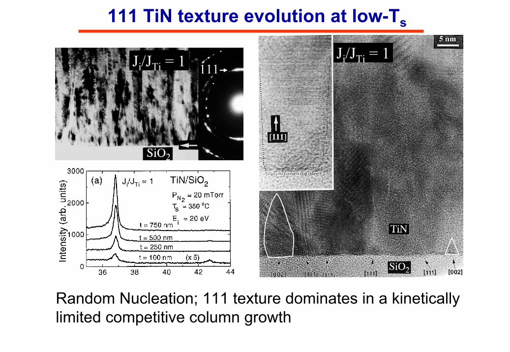
111 TiN texture evolution at low-Ts
Random Nucleation; 111 texture dominates in a kinetically limited competitive column growth
Ji/JTi = 1 Ji/JTi = 1111
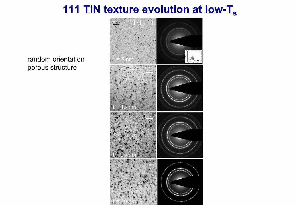
111 TiN texture evolution at low-Ts
random orientationporous structure
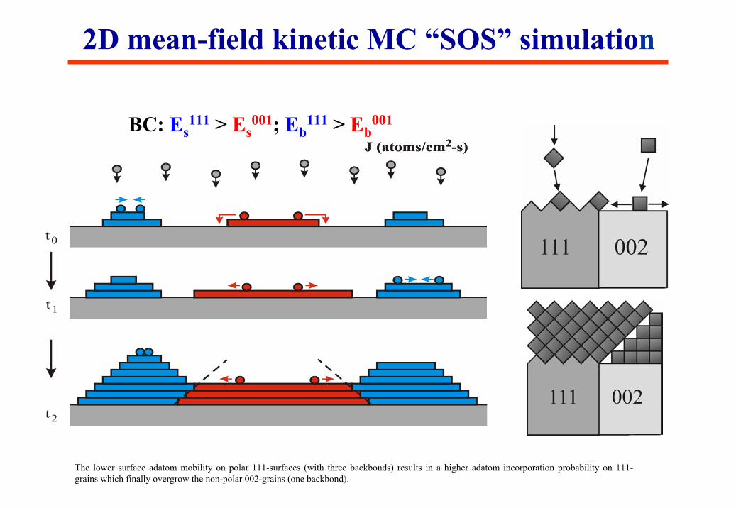
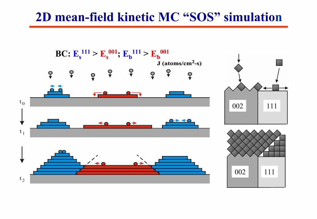
BC: Es111 > Es
001; Eb111 > Eb
001
2D mean-field kinetic MC “SOS” simulation
The lower surface adatom mobility on polar 111-surfaces (with three backbonds) results in a higher adatom incorporation probability on 111-grains which finally overgrow the non-polar 002-grains (one backbond).
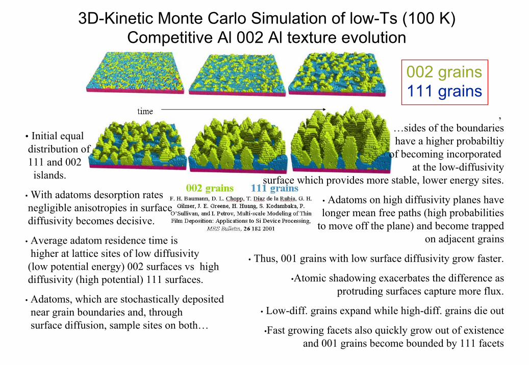
3D-Kinetic Monte Carlo Simulation of low-Ts (100 K)Competitive Al 002 Al texture evolution
002 grains111 grains
• Initial equaldistribution of111 and 002
islands.
• With adatoms desorption ratesnegligible anisotropies in surfacediffusivity becomes decisive.
• Average adatom residence time ishigher at lattice sites of low diffusivity
(low potential energy) 002 surfaces vs highdiffusivity (high potential) 111 surfaces.
• Adatoms, which are stochastically depositednear grain boundaries and, throughsurface diffusion, sample sites on both…
, …sides of the boundarieshave a higher probabiltiy
of becoming incorporated at the low-diffusivity
surface which provides more stable, lower energy sites.
• Adatoms on high diffusivity planes havelonger mean free paths (high probabilities
to move off the plane) and become trappedon adjacent grains
• Thus, 001 grains with low surface diffusivity grow faster.
•Atomic shadowing exacerbates the difference asprotruding surfaces capture more flux.
• Low-diff. grains expand while high-diff. grains die out
•Fast growing facets also quickly grow out of existenceand 001 grains become bounded by 111 facets
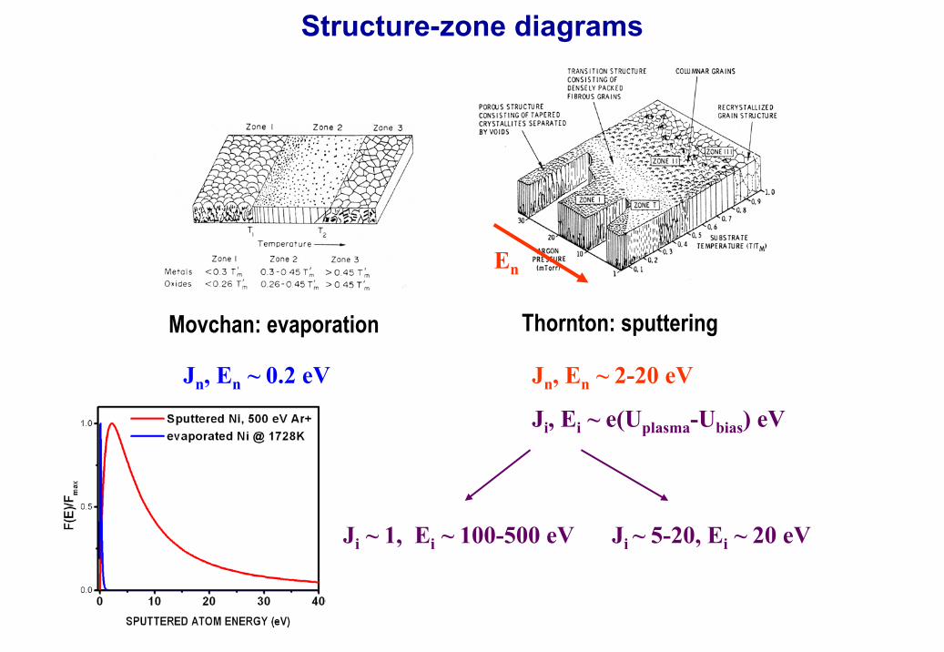
Structure-zone diagrams
Movchan: evaporation Thornton: sputtering
En
Jn, En ~ 0.2 eV Jn, En ~ 2-20 eV
Ji, Ei ~ e(Uplasma-Ubias) eV
Ji ~ 5-20, Ei ~ 20 eVJi ~ 1, Ei ~ 100-500 eV
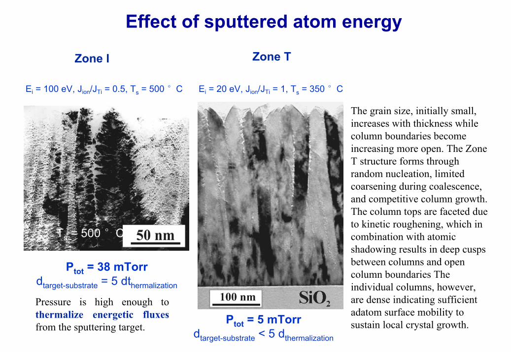
Pressure is high enough to thermalize energetic fluxesfrom the sputtering target.
Ei = 100 eV, Jion/JTi = 0.5, Ts = 500 °C
The grain size, initially small, increases with thickness while column boundaries become increasing more open. The Zone T structure forms through random nucleation, limited coarsening during coalescence, and competitive column growth. The column tops are faceted due to kinetic roughening, which in combination with atomic shadowing results in deep cusps between columns and open column boundaries The individual columns, however, are dense indicating sufficient adatom surface mobility to sustain local crystal growth.
Effect of sputtered atom energy
Ts = 500 °C
Ptot = 38 mTorrdtarget-substrate = 5 dthermalization
Ptot = 5 mTorrdtarget-substrate < 5 dthermalization
Zone I Zone T
Ei = 20 eV, Jion/JTi = 1, Ts = 350 °C
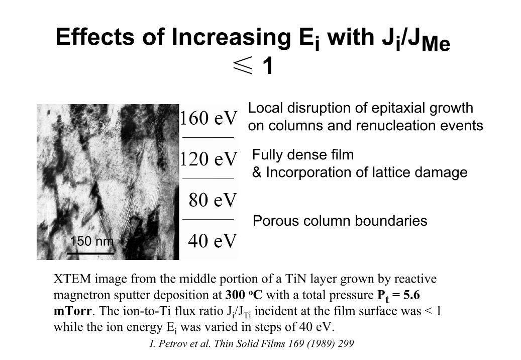
Effects of Increasing Ei with Ji/JMe≤ 1
XTEM image from the middle portion of a TiN layer grown by reactive magnetron sputter deposition at 300 oC with a total pressure Pt = 5.6 mTorr. The ion-to-Ti flux ratio Ji/JTi incident at the film surface was < 1 while the ion energy Ei was varied in steps of 40 eV.
I. Petrov et al. Thin Solid Films 169 (1989) 299
150 nmPorous column boundaries
Fully dense film& Incorporation of lattice damage
Local disruption of epitaxial growthon columns and renucleation events
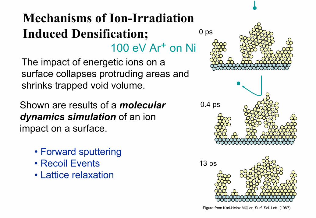
The impact of energetic ions on a surface collapses protruding areas and shrinks trapped void volume.
Shown are results of a molecular dynamics simulation of an ion impact on a surface.
• Forward sputtering• Recoil Events• Lattice relaxation
黮Figure from Karl-Heinz M ler, Surf. Sci. Lett. (1987)
Mechanisms of Ion-IrradiationInduced Densification;
100 eV Ar+ on Ni0 ps
0.4 ps
13 ps
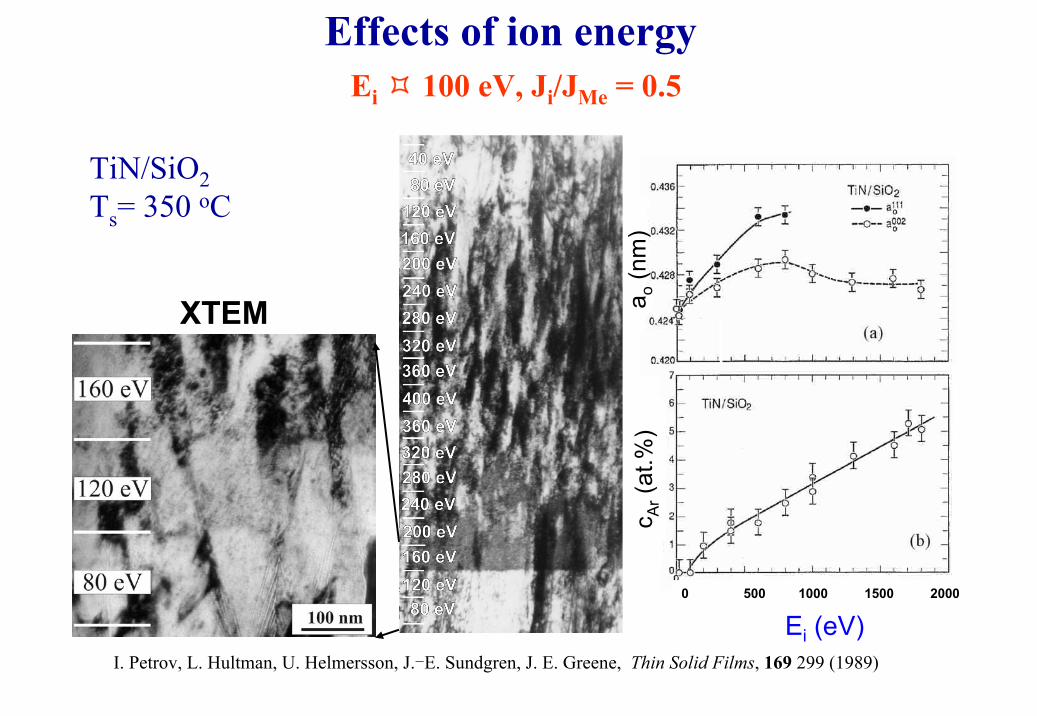
Effects of ion energyEi 100 eV, Ji/JMe = 0.5
TiN/SiO2Ts= 350 oC
XTEM
0 500 1000 1500 2000
Ei (eV)c A
r(a
t.%)
a o(n
m)
I. Petrov, L. Hultman, U. Helmersson, J.-E. Sundgren, J. E. Greene, Thin Solid Films, 169 299 (1989)
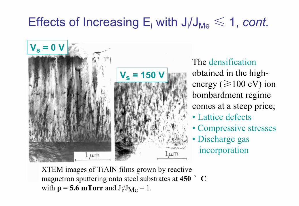
Effects of Increasing Ei with Ji/JMe ≤ 1, cont.
XTEM images of TiAlN films grown by reactive magnetron sputtering onto steel substrates at 450 °Cwith p = 5.6 mTorr and Ji/JMe = 1.
The densificationobtained in the high-energy (≥100 eV) ion bombardment regime comes at a steep price;• Lattice defects • Compressive stresses• Discharge gas
incorporation
Vs = 0 V
Vs = 150 V
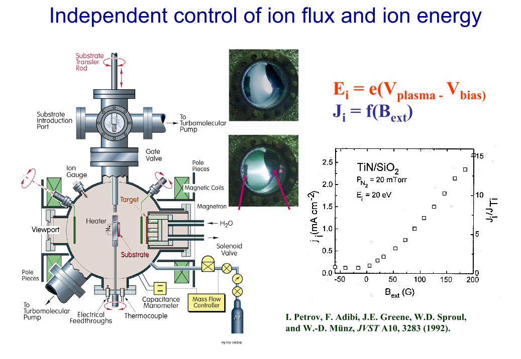
Independent control of ion flux and ion energy
Ei = e(Vplasma - Vbias)Ji = f(Bext)
I. Petrov, F. Adibi, J.E. Greene, W.D. Sproul, and W.-D. Münz, JVST A10, 3283 (1992).
0 50 100
0.415
0.416
0.417
0.418
0.419 (c)
a o (nm
)
<Ed> (eV/Metal atom)
1.0
1.1
1.2(b)
N/(T
i + A
l)
0.0
0.2
0.4
0.6
0.8
1.0(a)
I 002/
(I 111 +
I 002)
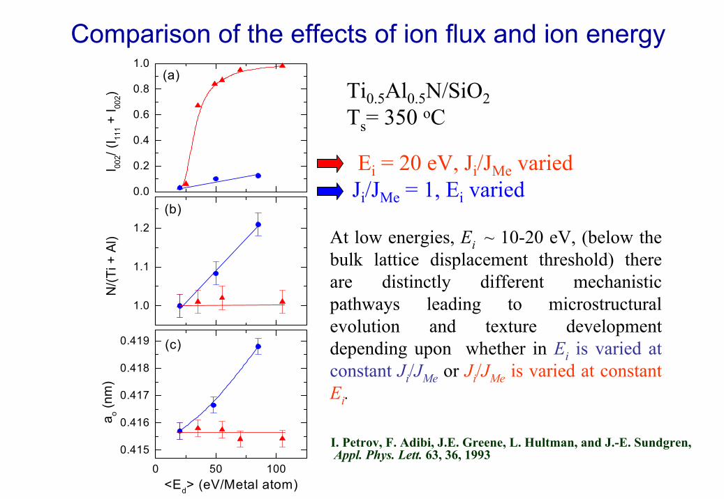
Ei = 20 eV, Ji/JMe variedJi/JMe = 1, Ei varied
Ti0.5Al0.5N/SiO2Ts= 350 oC
At low energies, Ei ~ 10-20 eV, (below the bulk lattice displacement threshold) there are distinctly different mechanistic pathways leading to microstructural evolution and texture development depending upon whether in Ei is varied at constant Ji/JMe or Ji/JMe is varied at constant Ei.
Comparison of the effects of ion flux and ion energy
I. Petrov, F. Adibi, J.E. Greene, L. Hultman, and J.-E. Sundgren,Appl. Phys. Lett. 63, 36, 1993
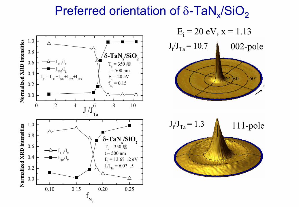
Preferred orientation of δ-TaNx/SiO2
0.10 0.15 0.20 0.25
0.0
0.2
0.4
0.6
0.8
1.0
Ts 癈 = 350 t = 500 nmEi = 13.6? .2 eVJi/JTa = 6.0? .5
δ-TaNx/SiO2
I111/IΣ I002/IΣ
Nor
mal
ized
XR
D in
tens
ities
fN2
0 2 4 6 8 10
0.0
0.2
0.4
0.6
0.8
1.0
Ts癈 = 350
t = 500 nmEi = 20 eVfN
2
= 0.15
δ-TaNx/SiO2
IΣ = I111+I002+I022+I113
I111/IΣ I002/IΣ
Nor
mal
ized
XR
D in
tens
ities
Ji/JTa
002-pole
111-pole
Ji/JTa = 10.7
Ji/JTa = 1.3
Ψ=30°
60°φ
Ei = 20 eV, x = 1.13
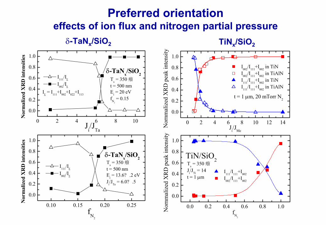
Preferred orientation effects of ion flux and nitrogen partial pressure
0.10 0.15 0.20 0.25
0.0
0.2
0.4
0.6
0.8
1.0
Ts癈 = 350
t = 500 nmEi = 13.6? .2 eVJi/JTa = 6.0? .5
δ-TaNx/SiO2
I111/IΣ I002/IΣ
Nor
mal
ized
XR
D in
tens
ities
fN2
0 2 4 6 8 10
0.0
0.2
0.4
0.6
0.8
1.0
Ts 癈 = 350 t = 500 nmEi = 20 eVfN
2
= 0.15
δ-TaNx/SiO2
IΣ = I111+I002+I022+I113
I111/IΣ I002/IΣ
Nor
mal
ized
XR
D in
tens
ities
Ji/JTa0 2 4 6 8 10 12 14
0.0
0.2
0.4
0.6
0.8
1.0
t = 1 µm, 20 mTorr N2
I002/I111+I002 in TiN I002/I111+I002 in TiAlN I111/I111+I002 in TiN I111/I111+I002 in TiAlN
Nor
nmal
ized
XR
D p
eak
inte
nsity
Ji/JMe
0.0 0.2 0.4 0.6 0.8 1.0
0.0
0.2
0.4
0.6
0.8
1.0
I111/I111+I002 I002/I111+I002
TiN/SiO2Ts
癈 = 350 Ji/JTi = 14t = 1 µm
Nor
nmal
ized
XR
D p
eak
inte
nsity
fN2
δ-TaNx/SiO2 TiNx/SiO2
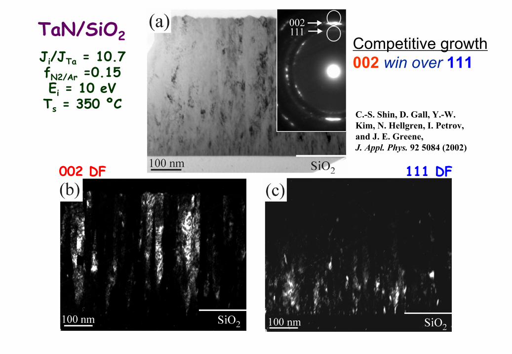
002 DF 111 DF
TaN/SiO2Ji/JTa = 10.7fN2/Ar =0.15Ei = 10 eVTs = 350 ºC
Competitive growth002 win over 111
C.-S. Shin, D. Gall, Y.-W. Kim, N. Hellgren, I. Petrov, and J. E. Greene,J. Appl. Phys. 92 5084 (2002)
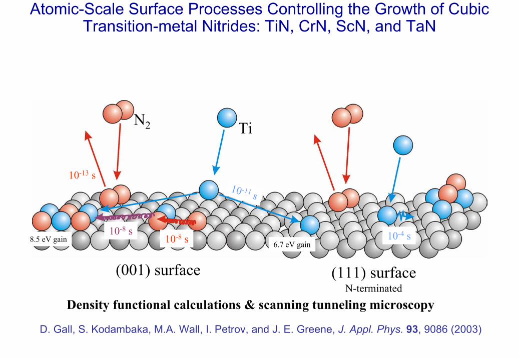
Atomic-Scale Surface Processes Controlling the Growth of Cubic Transition-metal Nitrides: TiN, CrN, ScN, and TaN
(001) surface (111) surfaceN-terminated
6.7 eV gain
10-13 s
10-8 s10-8 s
10-11 s
10-4 s
N2 Ti
8.5 eV gain
Density functional calculations & scanning tunneling microscopy
D. Gall, S. Kodambaka, M.A. Wall, I. Petrov, and J. E. Greene, J. Appl. Phys. 93, 9086 (2003)
- Momentum transfer to surface .- θN on (002) due to
collisionally-induced dissociative chemisorptionof N2
+.
(111)
(002)
Ta
N
NTa
N
NTaTa
Ji,
fN2
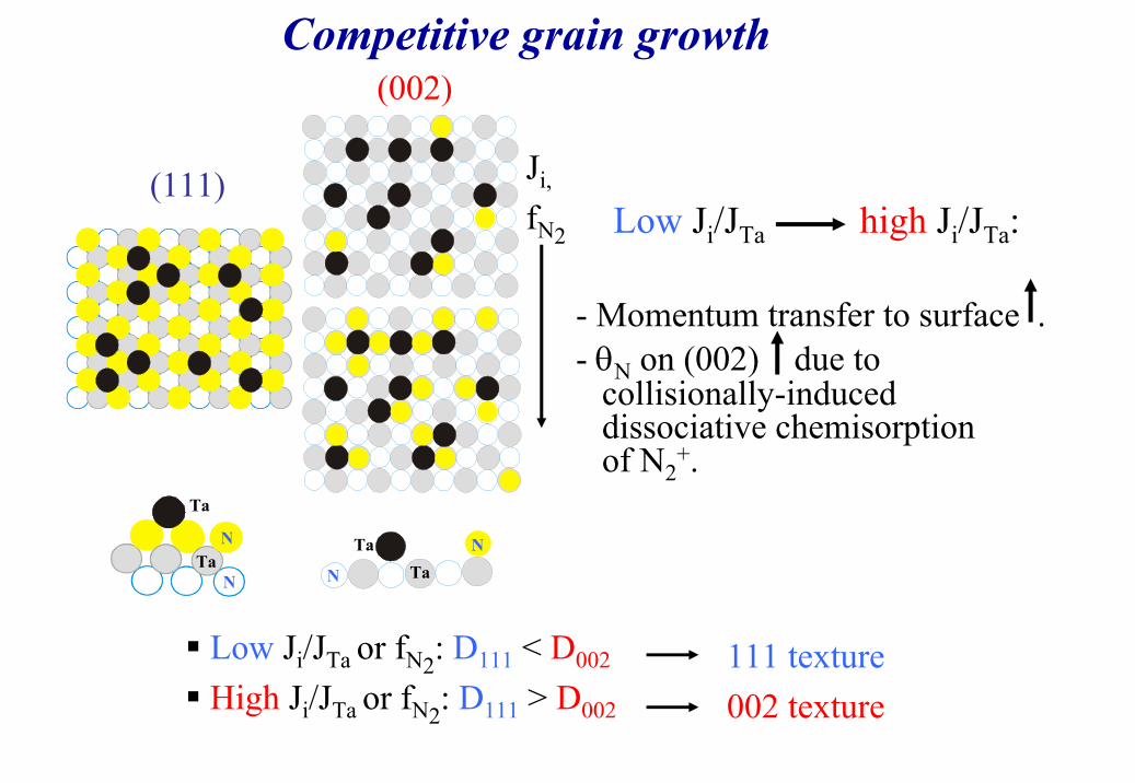
Competitive grain growth
Low Ji/JTa high Ji/JTa:
Low Ji/JTa or fN2: D111 < D002
High Ji/JTa or fN2: D111 > D002
111 texture002 texture
BC: Es111 > Es
001; Eb111 > Eb
001
2D mean-field kinetic MC “SOS” simulation
002
002
111
111
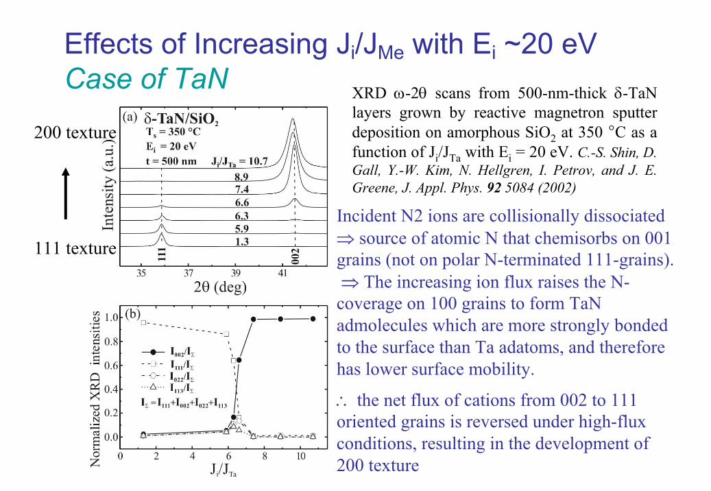
Effects of Increasing Ji/JMe with Ei ~20 eVCase of TaN XRD ω-2θ scans from 500-nm-thick δ-TaN
layers grown by reactive magnetron sputter deposition on amorphous SiO2 at 350 °C as a function of Ji/JTa with Ei = 20 eV. C.-S. Shin, D. Gall, Y.-W. Kim, N. Hellgren, I. Petrov, and J. E. Greene, J. Appl. Phys. 92 5084 (2002)
200 texture
111 texture
Incident N2 ions are collisionally dissociated ⇒ source of atomic N that chemisorbs on 001 grains (not on polar N-terminated 111-grains).⇒ The increasing ion flux raises the N-coverage on 100 grains to form TaN admolecules which are more strongly bonded to the surface than Ta adatoms, and therefore has lower surface mobility.
∴ the net flux of cations from 002 to 111 oriented grains is reversed under high-flux conditions, resulting in the development of 200 texture
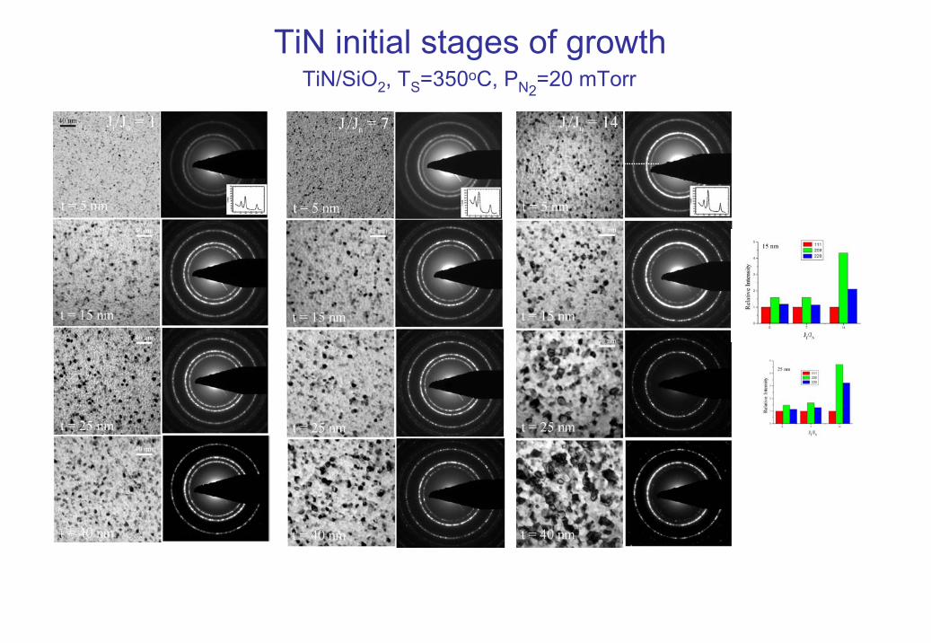
TiN initial stages of growthTiN/SiO2, TS=350oC, PN2=20 mTorr
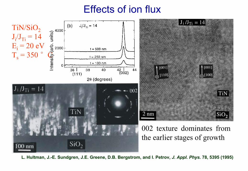
Effects of ion flux
TiN/SiO2Ji/JTi = 14Ei = 20 eVTs = 350 °C
002 texture dominates from the earlier stages of growth
L. Hultman, J.-E. Sundgren, J.E. Greene, D.B. Bergstrom, and I. Petrov, J. Appl. Phys. 78, 5395 (1995)
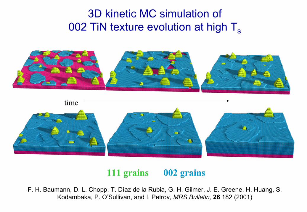
3D kinetic MC simulation of 002 TiN texture evolution at high Ts
time
111 grains 002 grains
F. H. Baumann, D. L. Chopp, T. Díaz de la Rubia, G. H. Gilmer, J. E. Greene, H. Huang, S. Kodambaka, P. O’Sullivan, and I. Petrov, MRS Bulletin, 26 182 (2001)
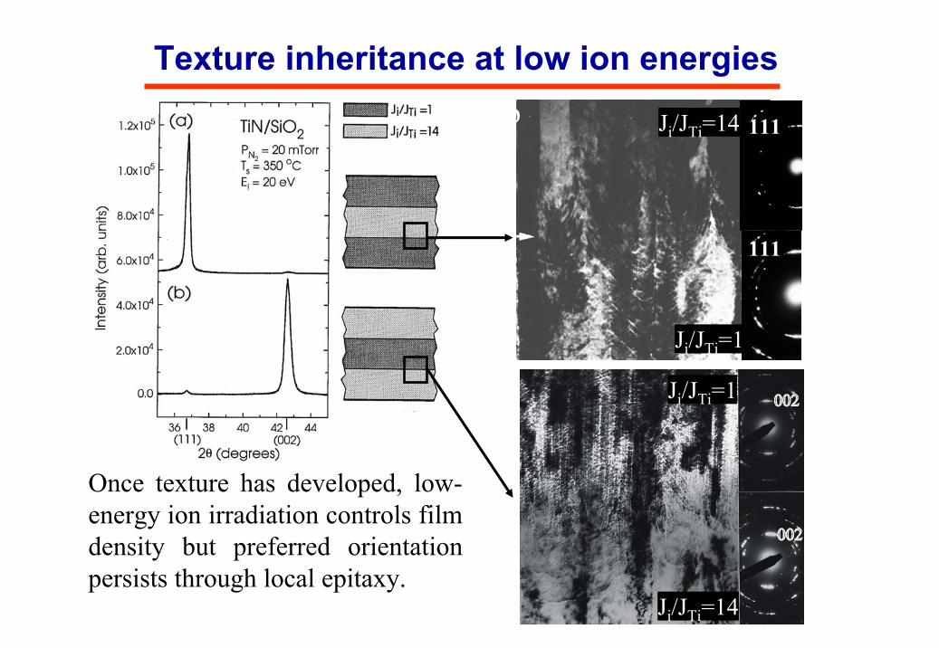
Texture inheritance at low ion energies
Once texture has developed, low-energy ion irradiation controls film density but preferred orientation persists through local epitaxy.
111
111
Ji/JTi=14
Ji/JTi=14
Ji/JTi=1
Ji/JTi=1
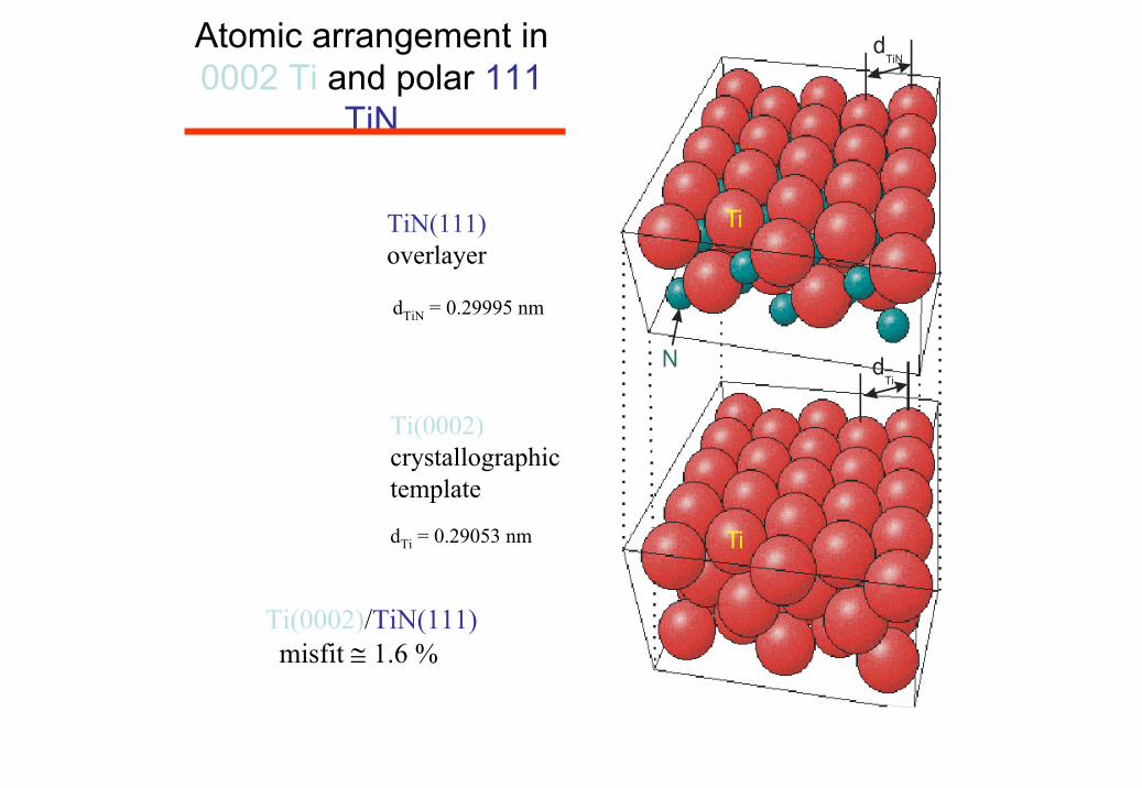
Ti
N
dTiN
dTi
Ti
TiN(111)overlayer
dTiN = 0.29995 nm
Ti(0002)crystallographictemplate
dTi = 0.29053 nm
Ti(0002)/TiN(111)misfit ≅ 1.6 %
Atomic arrangement in0002 Ti and polar 111
TiN
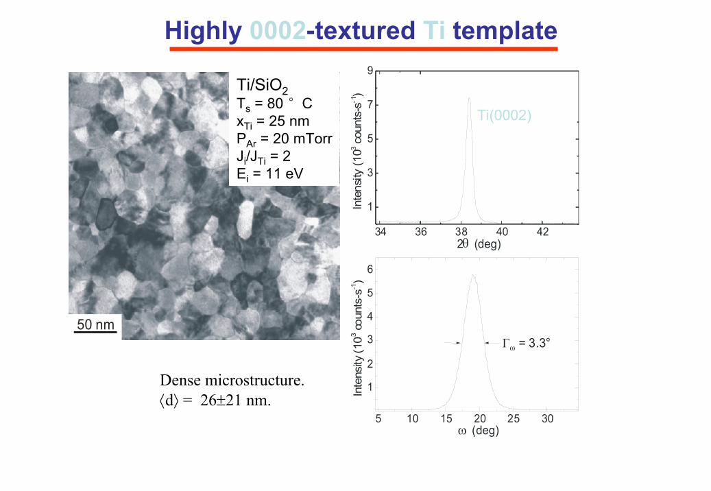
50 nm
Ti/SiO2Ts = 80 °CxTi = 25 nmPAr = 20 mTorrJi/JTi = 2Ei = 11 eV
Highly 0002-textured Ti template
34 36 38 40 42
1
3
5
7
9
Inte
nsity
(103
coun
ts-s
-1)
2θ (deg)
Ti(0002)
Dense microstructure.⟨d⟩ = 26±21 nm.
Γω = 3.3°
5 10 15 20 25 30
1
2
3
4
5
6
Inte
nsity
(103
coun
ts-s
-1)
ω (deg)
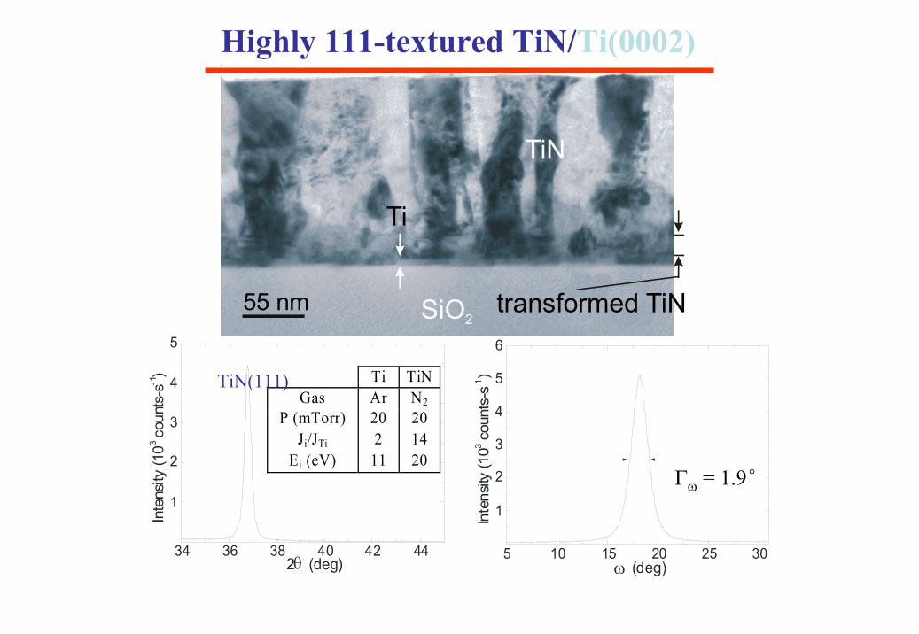
55 nm
Ti
TiN
transformed TiNSiO2
34 36 38 40 42 44
1
2
3
4
5
Inte
nsity
(103
coun
ts-s
-1)
2θ (deg)
Ti TiNGas Ar N2
P (mTorr) 20 20Ji/JTi 2 14
Ei (eV) 11 20
TiN(111)
5 10 15 20 25 30
1
2
3
4
5
6
Inte
nsity
(103
coun
ts-s
-1)
ω (deg)
Γω = 1.9°
Highly 111-textured TiN/Ti(0002)
002
022
50 nm 50 nm50 nm
022
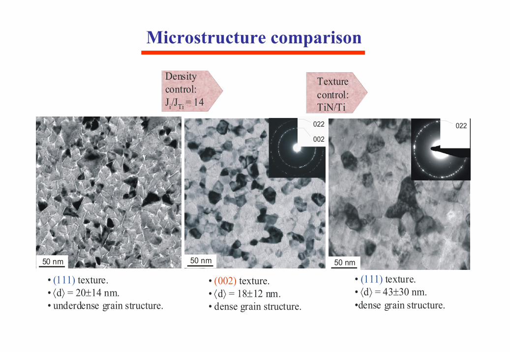
Densitycontrol:Ji/JTi = 14
Texturecontrol:TiN/Ti
• (111) texture.• ⟨d⟩ = 20±14 nm.• underdense grain structure.
• (002) texture.• ⟨d⟩ = 18±12 nm.• dense grain structure.
• (111) texture.• ⟨d⟩ = 43±30 nm.•dense grain structure.
Microstructure comparison
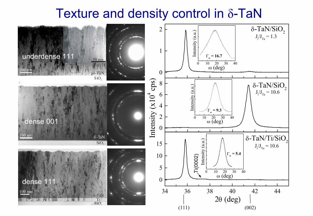
Texture and density control in δ-TaN
SiO2
100 nm δ-TaN
100 nm
SiO2
δ-TaN
50 nm
SiO2
Tiδ-TaN
100 nm
0
1
2
(002)(111)
δ-TaN/SiO2Ji/JTa = 1.3
0
2
4
6
8Ji/JTa = 10.6δ-TaN/SiO2
34 36 38 40 42 44
0
5
10
15
2θ (deg)
Inte
nsity
(x10
4 cps
)Ji/JTa = 10.6
δ-TaN/Ti/SiO2
Ti(0
002)
0 10 20 30 40
Inte
nsity
(a.u
.)
Γω = 16.7
ω (deg)
0 10 20 30 40
Inte
nsity
(a.u
.)
Γω = 9.3
ω (deg)
0 10 20 30 40
Inte
nsity
(a.u
.)
Γω = 5.4
ω (deg)
underdense 111
dense 111
dense 001