lm3263 high-current step-down dc-dc converter for … · · 2017-05-17lm3263 high-current...
TRANSCRIPT

1.8 VRFFE
Master LM3263
VIO
BGND PGND
VBATT2.7 V to 5.5 V
FB
ACB
SW
PACB SVDDPVIN
PA(s)
PA
2GVCC_PA
3G/4GVCC_PA
Output Voltage0.4 V to 3.6 VSCLK
SDATA
GPO1
SGND
Copyright © 2016, Texas Instruments Incorporated
Product
Folder
Sample &Buy
Technical
Documents
Tools &
Software
Support &Community
An IMPORTANT NOTICE at the end of this data sheet addresses availability, warranty, changes, use in safety-critical applications,intellectual property matters and other important disclaimers. PRODUCTION DATA.
LM3263SNVS837B –JUNE 2013–REVISED APRIL 2016
LM3263 High-Current Step-Down DC-DC Converter With MIPI® RF Front-EndControl Interface for RF Power Amplifiers
1
1 Features1• MIPI® RFFE Digital Control Interface• Operates from a Single Li-Ion Cell: 2.7 V to 5.5 V• Dynamically Adjustable Output Voltage: 0.4 V to
3.6 V (Typical) in PFM and PWM Modes• High-Efficiency PFM and PWM Modes With
Internal Seamless Transition• 2.5-A Maximum Load Current in PWM Mode• 2.7 MHz (Typical) Switching Frequency• ACB (Reduces Inductor Requirements and Size)• Internal Compensation• Current and Thermal Overload Protection• Very Small Solution Size: Approximately 9.1 mm2
2 Applications• Smartphones• RF PC Cards• Tablets, eBook Readers• Handheld Radios• Battery-Powered RF Devices
3 DescriptionThe LM3263 is a DC-DC converter optimized forpowering multi-mode multi-band RF power amplifiers(PAs) from a single lithium-ion cell. The LM3263steps down an input voltage from 2.7 V to 5.5 V to adynamically adjustable output voltage of 0.4 V to3.6 V. The output voltage is externally programmedthrough the RFFE Digital Control Interface and is setto ensure efficient operation at all power levels of theRF PA.
When operating in pulse width modulated (PWM)mode, the LM3263 produces a small and predictableamount of output voltage ripple thus meeting thepower and stringent spectral-compliance needs of RFPAs with minimal filtering and minimal excessheadroom. When operating in PFM mode, theLM3263 enables the lowest current consumptionacross PA output power level settings and thereforemaximizes system efficiency.
The LM3263 has a unique Active Current assist andanalog Bypass (ACB) feature to minimize inductorsize without any loss of output regulation for theentire battery voltage and RF output power range,until dropout. ACB provides a parallel current path,when needed, to limit the maximum inductor currentto 1.45 A (typical) while still driving a 2.5-A load. TheACB feature also enables operation with minimaldropout voltage.
Device Information(1)
PART NUMBER PACKAGE BODY SIZE (MAX)LM3263 DSBGA (16) 2.049 mm × 2.049 mm
(1) For all available packages, see the orderable addendum atthe end of the data sheet.
Typical Application

2
LM3263SNVS837B –JUNE 2013–REVISED APRIL 2016 www.ti.com
Product Folder Links: LM3263
Submit Documentation Feedback Copyright © 2013–2016, Texas Instruments Incorporated
Table of Contents1 Features .................................................................. 12 Applications ........................................................... 13 Description ............................................................. 14 Revision History..................................................... 25 Pin Configuration and Functions ......................... 36 Specifications......................................................... 4
6.1 Absolute Maximum Ratings ...................................... 46.2 ESD Ratings.............................................................. 46.3 Recommended Operating Conditions....................... 46.4 Thermal Information .................................................. 46.5 Electrical Characteristics........................................... 56.6 System Characteristics ............................................ 66.7 Typical Characteristics .............................................. 9
7 Detailed Description ............................................ 127.1 Overview ................................................................. 127.2 Functional Block Diagram ....................................... 137.3 Feature Description................................................. 137.4 Device Functional Modes........................................ 17
7.5 Programming........................................................... 197.6 Register Map........................................................... 22
8 Application Information....................................... 248.1 Application Information............................................ 248.2 Typical Application ................................................. 24
9 Power Supply Recommendations ...................... 2610 Layout Considerations ....................................... 27
10.1 Layout Guidelines ................................................. 2710.2 4. Layout Examples .............................................. 2810.3 DSBGA Package Assembly and Use ................... 36
11 Device and Documentation Support ................. 3711.1 Device Support...................................................... 3711.2 Documentation Support ........................................ 3711.3 Community Resources.......................................... 3711.4 Trademarks ........................................................... 3711.5 Electrostatic Discharge Caution............................ 3711.6 Glossary ................................................................ 37
12 Mechanical, Packaging, and OrderableInformation ........................................................... 37
4 Revision HistoryNOTE: Page numbers for previous revisions may differ from page numbers in the current version.
Changes from Revision A (August 2013) to Revision B Page
• Added Device Information and Pin Configuration and Functions sections, ESD Ratings and Feature Description,Device Functional Modes, Application and Implementation, Power Supply Recommendations, Layout, Device andDocumentation Support, and Mechanical, Packaging, and Orderable Information sections ................................................. 1
• Added Thermal Information table with revised RθJA value (from 50°C/W to 77.1°C/W) and additional thermal values. ....... 4
Changes from Original (June 2013) to Revision A Page
• Added new inductor to recommended table......................................................................................................................... 36

4 3 2 1
A
B
C
D
PVIN
PVIN
VIO
SCLK
SW
SW
SDATA
GPO1
FB
PGND
SGND
BGND
ACB
ACB
PACB
SVDD
4321
A
B
C
D
ACB
ACBFB
SW
SW
PGND
SGND
BGND PACB
VIO SDATA
SCLK GPO1 SVDD
PVIN
PVIN
3
LM3263www.ti.com SNVS837B –JUNE 2013–REVISED APRIL 2016
Product Folder Links: LM3263
Submit Documentation FeedbackCopyright © 2013–2016, Texas Instruments Incorporated
5 Pin Configuration and Functions
YFQ Package16-Pin DSBGA
Top View
YFQ Package16-Pin DSBGABottom View
Pin FunctionsPIN
TYPE DESCRIPTIONNAME NUMBER
ACBA4
Output ACB and analog bypass output. Connect to the output at the output filter capacitor.C4
BGND B3 Ground ACB, analog bypass ground, and digital ground.FB C3 Input Feedback analog input. Connect to the output at the output filter capacitor.GPO1 D2 Output General purpose output. Also used to reconfigure USID.PACB B4 Power ACB power supply inputPGND A3 Ground Power ground to the internal NFET switch
PVINA1
Power Power supply voltage input to the internal PFET switchB1
SCLK D1 Digital/Input Digital control interface RFFE Bus clock input. Typically connected to RFFE master onRF or baseband IC. SCLK must be held low when VIO is not applied.
SDATA C2 DigitalInput/Output
Digital control interface RFFE bus data input/output. Typically connected to RFFEmaster on RF or baseband IC. SDATA must be held low when VIO is not applied.
SGND D3 Ground Signal analog ground (low current)SVDD D4 Power Analog power supply voltage
SWA2
Analog Switching node connection to the internal PFET switch and NFET synchronousrectifier.B2
VIO C1 InputVIO functions as the RFFE interface reference voltage. VIO also functions as reset andenable input to the LM3263. Typically connected to voltage regulator controlled by RFor baseband IC.

4
LM3263SNVS837B –JUNE 2013–REVISED APRIL 2016 www.ti.com
Product Folder Links: LM3263
Submit Documentation Feedback Copyright © 2013–2016, Texas Instruments Incorporated
(1) Stresses beyond those listed under Absolute Maximum Ratings may cause permanent damage to the device. These are stress ratingsonly, which do not imply functional operation of the device at these or any other conditions beyond those indicated under RecommendedOperating Conditions. Exposure to absolute-maximum-rated conditions for extended periods may affect device reliability.
(2) All voltages are with respect to the potential at the GND pins.(3) Abs Max for FB, SW, GPO1, ACB, VIO, SDATA, SCLK is the lessor of VIN + 0.2 V, or 6 V.(4) Internal thermal shutdown circuitry protects the device from permanent damage. Thermal shutdown engages at TJ = 150°C (typical) and
disengages at TJ = 125°C (typical).
6 Specifications
6.1 Absolute Maximum Ratingsover operating free-air temperature range (unless otherwise noted) (1) (2)
MIN MAX UNITVBATT pins to GND (PVIN, SVDD, PACB to PGND, SGND, BGND) –0.2 6 VFB, SW, GPO1, ACB, VIO, SDATA, SCLK GND – 0.2 V See (3) VContinuous power dissipation (4) Internally limitedMaximum operating junction temperature, TJ-MAX 150 °CMaximum lead temperature (soldering 10 seconds) 260 °CStorage temperature, Tstg −65 150 °C
(1) JEDEC document JEP155 states that 500-V HBM allows safe manufacturing with a standard ESD control process.(2) JEDEC document JEP157 states that 250-V CDM allows safe manufacturing with a standard ESD control process.
6.2 ESD RatingsVALUE UNIT
V(ESD) Electrostatic dischargeHuman-body model (HBM), per ANSI/ESDA/JEDEC JS-001 (1) ±1000
VCharged-device model (CDM), per JEDEC specification JESD22-C101 (2) ±250
(1) In applications where high power dissipation and/or poor package thermal resistance is present, the maximum ambient temperature mayhave to be de-rated. Maximum ambient temperature (TA-MAX) is dependent on the maximum operating junction temperature (TJ-MAX-OP =125°C), the maximum power dissipation of the device in the application (PD-MAX), and the junction-to ambient thermal resistance of thepart/package in the application (RθJA), as given by the following equation: TA-MAX = TJ-MAX-OP – (RθJA × PD-MAX). At higher power levelsduty cycle usage is assumed to drop (that is, maximum power 12.5% usage is assumed) for GSM/GPRS mode.
6.3 Recommended Operating Conditionsover operating free-air temperature range (unless otherwise noted)
MIN MAX UNITInput voltage range PVIN, SVDD, PACB 2.7 5.5 VInput voltage range VIO 1.65 1.95 VRecommended current load 0 2.5 AJunction temperature, TJ –30 125 °CAmbient temperature, TA
(1) –30 90 °C
(1) For more information about traditional and new thermal metrics, see the Semiconductor and IC Package Thermal Metrics applicationreport, SPRA953.
6.4 Thermal Information
THERMAL METRIC (1)LM3263
UNITYFQ (DSBGA)16 PINS
RθJA Junction-to-ambient thermal resistance 77.1 °C/WRθJC(top) Junction-to-case (top) thermal resistance 0.4 °C/WRθJB Junction-to-board thermal resistance 15.4 °C/WψJT Junction-to-top characterization parameter 2.0 °C/WψJB Junction-to-board characterization parameter 15.1 °C/W

5
LM3263www.ti.com SNVS837B –JUNE 2013–REVISED APRIL 2016
Product Folder Links: LM3263
Submit Documentation FeedbackCopyright © 2013–2016, Texas Instruments Incorporated
(1) All voltages are with respect to the potential at the GND pins.(2) Minimum and Maximum limits are specified by design, test, or statistical analysis.(3) The parameters in Electrical Characteristics are tested under open loop conditions at PVIN = SVDD = PACB = 3.8 V.(4) Shutdown current includes leakage current of PFET.(5) IQ specified here is when the part is not switching.(6) Current limit is built-in, fixed, and not adjustable.
6.5 Electrical CharacteristicsUnless otherwise noted, all limits apply to the Typical Application with VBATT = 3.8 V (= PVIN = SVDD = PACB), VIO = 1.8 V,TJ = 25°C. (1) (2) (3)
PARAMETER TEST CONDITIONS MIN TYP MAX UNIT
VFB,MINFeedback voltage atminimum setting
VSET[7:0] = 1Bh, SMPS_CFG[5] = 1b 0.4VVSET[7:0] = 1Bh, SMPS_CFG[5] = 1b
−30°C ≤ TJ = TA ≤ 90°C 0.35 0.45
VFB,MAXFeedback voltage atmaximum setting
VSET[7:0] = F0h, VBATT = 3.9 V,SMPS_CFG[5] = 0b 3.6
VVSET[7:0] = F0h, VBATT = 3.9 V,SMPS_CFG[5] = 0b−30°C ≤ TJ = TA ≤ 90°C
3.492 3.708
ISHDN Shutdown supply currentSW = 0 V, VIO = 0 V (4) 0.02
µASW = 0 V, VIO = 0 V (4)
−30°C ≤ TJ = TA ≤ 90°C 4
IL-PWRLow-power mode supplycurrent VSET[7:0] = 00h 0.225 µA
IQ-PFMPFM mode supply currentinto SVDD
No switching (5), SMPS_CFG[5] = 1b 360µANo switching (5), SMPS_CFG[5] = 1b
−30°C ≤ TJ = TA ≤ 90°C 425
IQ PWM PWM mode supply currentNo switching (5), SMPS_CFG[5] = 0b 1240
µANo switching (5), SMPS_CFG[5] = 0b−30°C ≤ TJ = TA ≤ 90°C 1400
ILIM, PFET TransientPositive transient peakcurrent limit
VSET[7:0] = 64h (6) 1.9AVSET[7:0] = 64h (6)
−30°C ≤ TJ = TA ≤ 90°C 2.1
ILIM, PFET Steady-State
Positive steady-state peakcurrent limit
VSET[7:0] = 64h (6) 1.45AVSET[7:0] = 64h (6)
−30°C ≤ TJ = TA ≤ 90°C 1.35 1.65
ILIM, P-ACBPositive active current assistpeak current limit
VSET[7:0] = 64h (6) 1.7AVSET[7:0] = 64h (6)
−30°C ≤ TJ = TA ≤ 90°C 1.4 2
ILIM,NFET NFET current limit VSET[7:0] = A7h (6) −1.5 A
ƒOSCAverage Internal oscillatorfrequency
VSET[7:0] = A7h 2.7MHzVSET[7:0] = A7h
−30°C ≤ TJ = TA ≤ 90°C 2.43 2.97
IVIO-INVIO voltage average inputcurrent Average during a 26-MHz write 1.25 mA
VIORSTRFFE I/O voltage resetvoltage VIO toggled low 0.45 V
IINVIO VIO reset current VIO = 0.45 V −1 1 µAIIN SDATA, SCLK input current VIO = 1.95 V −1 1 µA
VIHInput high-level thresholdSDATA, SCLK 0.4 × VIO 0.7 ×
VIO V
VIL Input low-level thresholdSDATA, SCLK 0.3 × VIO 0.6 ×
VIO V
VIH-GPO Input high-level thresholdGPO1
−30°C ≤ TJ = TA ≤ 90°C 1.35 V
VIL-GPO Input low-level thresholdGPO1 −30°C ≤ TJ = TA ≤ 90°C 0.67 V

6
LM3263SNVS837B –JUNE 2013–REVISED APRIL 2016 www.ti.com
Product Folder Links: LM3263
Submit Documentation Feedback Copyright © 2013–2016, Texas Instruments Incorporated
Electrical Characteristics (continued)Unless otherwise noted, all limits apply to the Typical Application with VBATT = 3.8 V (= PVIN = SVDD = PACB), VIO = 1.8 V,TJ = 25°C.(1)(2)(3)
PARAMETER TEST CONDITIONS MIN TYP MAX UNITVOH Output high-level threshold
SDATAISDATA = 2 mA VIO × 0.8 VIO +
0.01 V
VOLOutput low-level thresholdSDATA ISDATA = –2 mA VIO ×
0.2 V
VOH-GPOOutput high-level thresholdGPO
IOUT = ±200 µAVIO – 0.15 VIO +
0.1 V
VOL-GPOOutput low-level thresholdGPO –0.4 0.3 V
VSET-LSB Output voltage LSB VSET[7:0] = A7h to A8h 15 mV
6.6 System CharacteristicsThe following spec table entries are specified by design and verifications providing the component values in the TypicalApplication are used (L = 1.5 µH, DCR = 120 mΩ, TOKO DFE201610MT-1R5N, CIN = 10 µF, 6.3 V, 0402, SamsungCL05A106MP5NUN, COUT = 10 µF + 4.7 µF + 3 × 1 µF; 10 V, 0402, Samsung CL05A106MP5NUN, CL05A475MPNRN;6.3 V, 0201, TDK, C0603X5R0J105M). These parameters are not verified by production testing. Minimum and maximumvalues are specified over the ambient temperature range TA = –30°C to +90°C. Typical values are specified at VBATT = 3.8 V(= PVIN = SVDD = PACB), VIO = 1.8 V, SMPS_CFG = 20h, and TA = 25°C, unless otherwise stated.
PARAMETER TEST CONDITIONS MIN TYP MAX UNIT
TON
Turnon time (time for output to reach95% of 3.4-V value from the end ofthe SCLK pulse)
VBATT = 4.2 V, VSET[7:0] =00h to E3h,VSET = 3.4 V, IOUT ≤ 1 mA 50 µs
TRESPONSE
Time for VOUT to rise from 0.09 V to3.4 V (3.07 V, 90% of delta VOUTfrom the end of SCLK pulse)
VBATT = 3.8 V, RLOAD = 68 ΩVSET[7:0] = 06h to E3hSMPS_CFG[5] = 0b/1b
15
µs
Time for VOUT to fall from 3.4 V to0.09 V (0.42 V, 10% of delta VOUTfrom the end of SCLK pulse)
VBATT = 3.8 V, RLOAD = 68 ΩVSET[7:0] = E3h to 06hSMPS_CFG[5] = 0b/1b
15
Time for VOUT to rise from 0.8 V to3.3 V (3.05V, 90% of delta VOUT fromthe end of SCLK pulse)
VBATT = 3.8 V, RLOAD = 20 ΩVSET[7:0] =36h to DCh 7.4 12
Time for VOUT to fall from 3.3 V to 0.8V (1.05 V, 10% of delta VOUT fromthe end of SCLK pulse)
VBATT = 3.8 V, RLOAD = 20 ΩVSET[7:0] = DCh to 36h 6.8 12
Time for VOUT to rise from 1.4 V to3.4 V (3.2 V, 90% of delta VOUT fromthe end of SCLK pulse)
VBATT = 3.8 V, RLOAD = 6.8 ΩVSET[7:0] = 5Eh to E3h 10
Time for VOUT to fall from 3.4 V to 1.4V (1.6 V, 10% of delta VOUT from theend of SCLK pulse)
VBATT = 3.8 V, RLOAD = 6.8 ΩVSET[7:0] = E3h to 5Eh 10
Time for VOUT to rise from 1.8 V to2.8 V (2.7 V, 90% of delta VOUT fromthe end of SCLK pulse)
VBATT = 3.8 V, RLOAD = 2.2 ΩVSET[7:0] = 78h to BBhSMPS_CFG[5] = 0b
15
Time for VOUT to fall from 2.8 V to 1.8V (1.9 V, 10% of delta VOUT from theend of SCLK pulse)
VBATT = 3.8 V, RLOAD = 2.2 ΩVSET[7:0] = BBh to 78hSMPS_CFG[5] = 0b
15
TBypassTime for VSET to rise from 0.09V toPVIN after BYPASS transition (90%)
VBATT = 3.6 V, IOUT ≤ 1 mA,VSET[7:0] = 06h to FFh 20 µs
Rtot-dropTotal dropout resistance in bypassmode
VSET[7:0] = FAh, Max value at VBATT= 3.1 V, Inductor DCR ≤ 151 mΩ 45 55 mΩ

7
LM3263www.ti.com SNVS837B –JUNE 2013–REVISED APRIL 2016
Product Folder Links: LM3263
Submit Documentation FeedbackCopyright © 2013–2016, Texas Instruments Incorporated
System Characteristics (continued)The following spec table entries are specified by design and verifications providing the component values in the TypicalApplication are used (L = 1.5 µH, DCR = 120 mΩ, TOKO DFE201610MT-1R5N, CIN = 10 µF, 6.3 V, 0402, SamsungCL05A106MP5NUN, COUT = 10 µF + 4.7 µF + 3 × 1 µF; 10 V, 0402, Samsung CL05A106MP5NUN, CL05A475MPNRN;6.3 V, 0201, TDK, C0603X5R0J105M). These parameters are not verified by production testing. Minimum and maximumvalues are specified over the ambient temperature range TA = –30°C to +90°C. Typical values are specified at VBATT = 3.8 V(= PVIN = SVDD = PACB), VIO = 1.8 V, SMPS_CFG = 20h, and TA = 25°C, unless otherwise stated.
PARAMETER TEST CONDITIONS MIN TYP MAX UNIT
(1) Current limit is built-in, fixed, and not adjustable.(2) Linearity limits are ±3% or ±50 mV whichever is larger.(3) Ripple voltage must be measured at COUT electrode on a well-designed PC board using suggested inductor and capacitors.
IOUT Maximum load current in PWM mode Switcher + ACB 2.5
AIOUT, PUMaximum output transient pullupcurrent limit Switcher + ACB (1) 3
IOUT, PD,PWM
PWM maximum output transientpulldown current limit Switcher + ACB (1) −3
IOUT,MAX_PFM
Maximum output load current in PFMmode VBATT = 3.8 V, VSET = 3.2 V 60 mA
Linearity Linearity in control range of VSET =0.4 V to 3.6 V
VBATT = 3.9 V (2), Monotonic in nature;VSET[7:0] = 1Bh to F0h,SMPS_CFG[5] = 0b
–3% 3%
–50 50 mV
η Efficiency
VBATT = 3.8 V, VSET= 0.5 V,IOUT = 5mA 52% 56%
VBATT = 3.8 V, VSET= 1.8 V,IOUT = 10 mA 78% 82%
VBATT = 3.8 V, VSET= 1.6 V,IOUT = 130 mA 83% 89%
VBATT = 3.8 V, VSET = 2.5 V,IOUT = 250 mA 90% 94%
VBATT = 3.8 V, VSET = 3.4 V,IOUT = 550 mA 93% 95%
VBATT = 3.8 V, VSET = 1 V,IOUT = 400 mA, SMPS_CFG[5] = 0b 81% 85%
VBATT = 3.8 V, VSET = 3.5 V,IOUT = 1900 mA, SMPS_CFG[5] = 0b 89% 92%
VRIPPLE
2.7-MHz PWM normal operationripple
VBATT = 3.2 V to 4.3 V, VSET = 0.4 Vto 3.6 V, RLOAD = 1.9 Ω (3)
SMPS_CFG[5]= 0b1 3
mVpp
Ripple voltage at pulse skippingcondition
VBATT = 3.2 V, VSET = 3 V,RLOAD = 1.9 Ω (3)
SMPS_CFG[5]= 0b8
PFM ripple voltage
VBATT = 3.2 V, VSET = 3 V,IOUT = 40 mA 50
VBATT = 3.2 V, VSET = 2.5 V,IOUT = 10 mA 50
VBATT = 3.2 V, VSET< 0.5 V,IOUT = 5 mA 50
Line_tr Line transient response
VBATT = 3.6 V to 4.2 V,TR = TF = 10 µs,VSET = 3.2 V,IOUT = 500 mA
50 mVpk
Load_tr Load transient response
VSET = 3 V,TR = TF = 10 µs,IOUT = 0 A to 1.2 A,SMPS_CFG[5] = 0b
60 mVpk
Max DutyCycle Maximum duty cycle 100%

8
LM3263SNVS837B –JUNE 2013–REVISED APRIL 2016 www.ti.com
Product Folder Links: LM3263
Submit Documentation Feedback Copyright © 2013–2016, Texas Instruments Incorporated
System Characteristics (continued)The following spec table entries are specified by design and verifications providing the component values in the TypicalApplication are used (L = 1.5 µH, DCR = 120 mΩ, TOKO DFE201610MT-1R5N, CIN = 10 µF, 6.3 V, 0402, SamsungCL05A106MP5NUN, COUT = 10 µF + 4.7 µF + 3 × 1 µF; 10 V, 0402, Samsung CL05A106MP5NUN, CL05A475MPNRN;6.3 V, 0201, TDK, C0603X5R0J105M). These parameters are not verified by production testing. Minimum and maximumvalues are specified over the ambient temperature range TA = –30°C to +90°C. Typical values are specified at VBATT = 3.8 V(= PVIN = SVDD = PACB), VIO = 1.8 V, SMPS_CFG = 20h, and TA = 25°C, unless otherwise stated.
PARAMETER TEST CONDITIONS MIN TYP MAX UNIT
PFM_Freq Minimum PFM frequency
VBATT = 3.2 V, VSET = 1 V,IOUT = 10 mA 100 160
KHzVBATT = 3.2 V, VSET = 0.5 V,IOUT = 5 mA 34 55
NSET VSET DAC number of bits Monotonic 8 Bits
TSETUPPower-up time (time for RFFE busactive after VIO applied) VIO = Low to 1.65 V 50 ns
TVIO-RST VIO supply reset timing VIO = 0.45 V 10 µs

2.6
2.8
3.0
3.2
3.4
3.6
2.5 3.0 3.5 4.0 4.5 5.0 5.5
OU
TP
UT
VO
LTA
GE
( V
)
INPUT VOLTAGE ( V ) C005
IOUT = 500mA
IOUT = 1.5A
60
65
70
75
80
85
90
95
100
0 25 50 75 100 125 150
EF
FIC
IEN
CY
( %
)
OUTPUT CURRENT ( mA )
VOUT = 0.8VVOUT = 1.0VVOUT = 1.5VVOUT = 1.8VVOUT = 2.0VVOUT = 0.4V
C006
2.50
2.55
2.60
2.65
2.70
2.75
2.80
2.85
2.90
2.95
3.00
2.5 3.0 3.5 4.0 4.5 5.0 5.5
SW
ITC
HIN
G F
RE
QU
EN
CY
( M
Hz
)
INPUT VOLTAGE ( V ) C003
VOUT = 2.0V, IOUT = 500mA
0.0
0.5
1.0
1.5
2.0
2.5
3.0
3.5
4.0
0.0 0.5 1.0 1.5 2.0 2.5 3.0 3.5 4.0
OU
TP
UT
VO
LTA
GE
( V
)
VSET VOLTAGE ( V )
C004
VBATT = 4.2V RLOAD = 6.8
22 43 64 86 A7 C8 EA VSET_CTRL (hex)
2.5 3.0 3.5 4.0 4.5 5.0 5.5
300
325
350
375
400
425
450
INP
UT
CU
RR
EN
T (
µA
)
INPUT VOLTAGE (V) C001
VOUT = 1.0V @ PFM mode
0
2
4
6
8
10
2.5 3.0 3.5 4.0 4.5 5.0 5.5
INP
UT
CU
RR
EN
T (
mA
)
INPUT VOLTAGE ( V ) C002
VOUT = 2.0V @ PWM Mode
9
LM3263www.ti.com SNVS837B –JUNE 2013–REVISED APRIL 2016
Product Folder Links: LM3263
Submit Documentation FeedbackCopyright © 2013–2016, Texas Instruments Incorporated
6.7 Typical CharacteristicsVBATT = 3.8 V, TA = 25°C, unless otherwise noted
No load
Figure 1. Input Current (PFM) vs Input Voltage
No load
Figure 2. Input Current (PWM) vs Input Voltage
Figure 3. Average Switching Frequency vs Input Voltage Figure 4. Output Voltage vs VSET_CTRL Setting
VOUT = 3.4 V
Figure 5. Output Voltage vs Input Voltage
Auto-PFM Mode IOUT = 10 mA to 150 mA
Figure 6. Efficiency vs Load Current

TIME ( 20µs/DIV )
C011
VOUT (2V/DIV)
SDATA (2V/DIV)
IOUT (1A/DIV)
VOUT
IOUT
5mVac/DIV
50mA/DIV
100s/DIV
60
65
70
75
80
85
90
95
100
1.00 1.25 1.50 1.75 2.00 2.25 2.50
EF
FIC
IEN
CY
( %
)
OUTPUT CURRENT ( A )
VOUT = 2.0VVOUT = 2.5VVOUT = 3.0VVOUT = 3.5V
C009
TIME ( 20µs/DIV )
C010
VOUT (2V/DIV)
SDATA (2V/DIV)
IOUT (500mA/DIV)
70
75
80
85
90
95
100
100 200 300 400 500 600 700 800
EF
FIC
IEN
CY
( %
)
OUTPUT CURRENT ( mA )
VOUT = 1.6VVOUT = 2.0VVOUT = 2.5VVOUT = 3.0VVOUT = 3.5V
C007
70
75
80
85
90
95
100
100 200 300 400 500 600 700 800 900 1,000
EF
FIC
IEN
CY
( %
)
OUTPUT CURRENT ( mA )
VOUT = 1.6VVOUT = 2.0VVOUT = 2.5VVOUT = 3.0VVOUT = 3.5V
C008
10
LM3263SNVS837B –JUNE 2013–REVISED APRIL 2016 www.ti.com
Product Folder Links: LM3263
Submit Documentation Feedback Copyright © 2013–2016, Texas Instruments Incorporated
Typical Characteristics (continued)VBATT = 3.8 V, TA = 25°C, unless otherwise noted
Auto-PFM Mode IOUT = 150 mA to 750 mA
Figure 7. Efficiency vs Load Current
Forced PWM Mode IOUT = 100 mA to 1000 mA
Figure 8. Efficiency vs Load Current
Forced PWM Mode IOUT = 1 A to 2.5 A
Figure 9. Efficiency vs Load Current
Auto PFM VOUT = 0.4 V to 3.4 V RLOAD = 6.8 Ω
Figure 10. VOUT Transient
Forced PWM VOUT = 1.4 V to 3.4 V RLOAD = 1.9 Ω
Figure 11. VOUT Transient
PFM Mode VOUT = 1 V IOUT= 0 mA to 60 mA
Figure 12. Load Transient

SW
IIND
VOUT
1A/DIV
2V/DIV
1V/DIV
20s/DIV100s/DIV
VOUT
VBATT
50mVac/DIV
500mV/DIV
VOUT
VBATT
50mVac/DIV
500mV/DIV
100s/DIV
VOUT
IOUT
100mVac/DIV
500mA/DIV
100s/DIV
VOUT
IOUT
50mVac/DIV
200mA/DIV
100s/DIV
VOUT
IOUT
50mVac/DIV
500mA/DIV
100s/DIV
11
LM3263www.ti.com SNVS837B –JUNE 2013–REVISED APRIL 2016
Product Folder Links: LM3263
Submit Documentation FeedbackCopyright © 2013–2016, Texas Instruments Incorporated
Typical Characteristics (continued)VBATT = 3.8 V, TA = 25°C, unless otherwise noted
VOUT = 2.5 V IOUT= 0 mA to 300 mA
Figure 13. Load Transient
VOUT = 3 V IOUT= 0 mA to 700 mA
Figure 14. Load Transient
VBATT = 4.2 V VOUT = 3 V IOUT= 0 mA to 1.2 A
Figure 15. Load Transient
VBATT = 3.6 V to 4.2 V VOUT = 2.5 V RLOAD = 6.8 Ω
Figure 16. Line Transient
VBATT = 3.6 V to 4.2 V VOUT = 1 V RLOAD = 6.8 Ω
Figure 17. Line Transient
VBATT = 4.2 V VOUT = 2.5 V RLOAD = 6.8 Ω to 0 Ω
Figure 18. Timed-Current Limit

12
LM3263SNVS837B –JUNE 2013–REVISED APRIL 2016 www.ti.com
Product Folder Links: LM3263
Submit Documentation Feedback Copyright © 2013–2016, Texas Instruments Incorporated
7 Detailed Description
7.1 OverviewThe LM3263 is a high-efficiency step-down DC-DC converter optimized to power the RF power amplifier (PA) incell phones, portable communication devices, or battery-powered RF devices with a single litium-Ion battery. Itoperates in modulated-frequency pulsed width modulation (PWM) mode for 2G transmissions (with MODE =Forced PWM (PWM only), register 01h SMPS_CFG [5] set to 0b), automatic mode transition between pulsefrequency modulation (PFM) and PWM for 3G/4G RF PA operation (with MODE = Auto-PFM (PFM/PWM),SMPS_CFG bit 5 set to 1b), or forced-bypass mode (with SMPS_CFG [4] set to 1b or REGISTER_0 [6:0] set to7Fh or register 03h VSET_CTRL [7:0] set to FEh-FFh). Power states are also in provided shutdown, low power,standby, and active modes. The DC-DC converter operates at active mode. Please see Figure 21 and RegisterMap.
PWM mode provides high efficiency and very low output-voltage ripple. In PWM-mode operation, the modulatedswitching frequency helps to reduce RF transmit noise. In PFM mode, the converter operates with reducedswitching frequencies and lower supply current to maintain high efficiencies. The forced-bypass mode allows theuser to drive the output directly from the input supply through a bypass FET. The shutdown mode turns theLM3263 off and reduces current consumption to 0.02 µA (typical).
In the PWM and PFM modes of operation, the output voltage of the LM3263 can be dynamically programmedfrom 0.4 V to 3.6 V (typical) by setting the VSET register. Current overload protection and thermal overloadprotection are also provided.
The LM3263 was engineered with Active Current assist and analog Bypass (ACB). This unique feature allowsthe converter to support maximum load currents of 2.5 A (minimum) while keeping a small footprint inductor andmeeting all of the transient behaviors required for operation of a multi-mode RF PA. The ACB circuit provides anadditional current path when the load current exceeds 1.45 A (typical) or as the switcher approaches dropout.Similarly, the ACB circuit allows the converter to respond with faster VSET output voltage transition times byproviding extra output current on rising and falling output edges. The ACB circuit also performs the function ofanalog bypass. Depending upon the input voltage, output voltage, and load current, the ACB circuit automaticallyand seamlessly transitions the converter into analog bypass, while maintaining output voltage regulation and lowoutput voltage ripple. Full bypass (100% duty cycle operation) occurs if the total dropout resistance in bypassmode (Rtot_drop = 45 mΩ) is insufficient to regulate the output voltage.
The device 16-pin DSBGA package is the best solution for space-constrained applications such as cell phonesand other hand-held devices. The high switching frequency, 2.7 MHz (typical) in PWM mode, reduces the size ofinput capacitors, output capacitor, and of the inductor. Use of a DSBGA package is best suited for opaque caseapplications and requires special design considerations for implementation (see Layout Considerations).

Q-MIPI CompliantRFFE
VSET DAC
Active Current Assist and
Analog Bypass (ACB)
SW
FB
BGNDPGND
PACBPVINVIOSCLKGPO1 SDATA
ENABLE
ACB
SGND
+
-
SVDD
Thermal Protection
CLK PWM RAMP
Error Amplifier
Internal Loop Compensation
Gate D
rive Circuits
Control Logic
+
-
SW
1.9 A Current Limit Protection
Copyright © 2016, Texas Instruments Incorporated
13
LM3263www.ti.com SNVS837B –JUNE 2013–REVISED APRIL 2016
Product Folder Links: LM3263
Submit Documentation FeedbackCopyright © 2013–2016, Texas Instruments Incorporated
7.2 Functional Block Diagram
7.3 Feature Description
7.3.1 PWM OperationThe LM3263 operates in PWM mode when forced-PWM mode operation is selected (SMPS_CFG [5] set to 0b).The switching frequency is modulated, and the switcher regulates the output voltage by changing the energy percycle to support the load required. During the first portion of each switching cycle, the control block in theLM3263 turns on the internal PFET switch. This allows current to flow from the input through the inductor and tothe output filter capacitor and load. The inductor limits the current to a ramp with a slope of (VBATT – VSET)/L, bystoring energy in its magnetic field.
During the second portion of each cycle, the control block turns the PFET switch off, blocking current flow fromthe input, and then turns the NFET synchronous rectifier on. The inductor draws current from ground through theNFET and to the output filter capacitor and load, which ramps the inductor current down with a slope of –VSET/L.The output filter capacitor stores charge when the inductor current is greater than the load current and releases itwhen the inductor current is less than the load current, smoothing the voltage across the load.
At the next rising edge of the clock, the cycle repeats. An increase of load pulls the output voltage down,increasing the error signal. As the error signal increases, the peak inductor current becomes higher thereforeincreasing the average inductor current. The output voltage is therefore regulated by modulating the PFET switchon time to control the average current sent to the load. The circuit generates a duty-cycle modulated rectangularsignal that is averaged using a low pass filter formed by the inductor and output capacitor. The output voltage isequal to the average of the duty-cycle modulated rectangular signal.

14
LM3263SNVS837B –JUNE 2013–REVISED APRIL 2016 www.ti.com
Product Folder Links: LM3263
Submit Documentation Feedback Copyright © 2013–2016, Texas Instruments Incorporated
Feature Description (continued)7.3.2 PFM OperationWhen auto-PFM mode operation is selected (SMPS_CFG [5] set to 1b), the LM3263 automatically transitionsfrom PWM operation into PFM operation if the average inductor current is less than 60 mA (minimum) and thedifference between VBATT – VSET ≥ 0.6 V. The switcher regulates the fixed output voltage by transferring a fixedamount of energy during each cycle and modulating the frequency to control the total power delivered to theoutput. The converter switches only as needed to support the demand of the load current, therefore maximizingefficiency. If there is an increase in load current during PFM mode to more than 120 mA (typical), the partautomatically transitions into PWM mode. A 20 mA (typical) hysteresis window exists between PFM and PWMtransitions. After a transient event, the part temporarily operates in PWM mode to quickly charge or discharge theoutput. This is true for start-up conditions or if the mode operation is changed from forced-PWM to auto-PFMmode (SMPS_CFG [5] toggled from 0b to 1b). Once the output reaches its target output voltage, and the load isless than 60 mA (minimum), then the device seamlessly transitions into PFM mode (assuming the device is notin forced-bypass condition).
7.3.3 Active Current Assist and Analog Bypass (ACB)The 3GPP time mask requirement for 2G requires high current to be sourced by the LM3263. These highcurrents are required for a small time during transients or under a heavy load. Overrating the switching inductorfor these higher currents increases the solution size and is not an optimum solution. Thus, to allow an optimalinductor size for such a load, an alternate current path is provided from the input supply through the ACB pin.Once the switcher current limit ILIM,PFET,SteadyState is reached, the ACB circuit starts providing the additional currentrequired to support the load. The ACB circuit also minimizes the dropout voltage by having the analog bypassFET in parallel with VSET. The LM3263 can provide up to 2.5 A (minimum) of current in bypass mode.
7.3.4 Bypass OperationThe bypass circuit provides an analog bypass function with very low dropout resistance (Rtot_drop = 45 mΩtypical). When SMPS_CFG [4] is set to 0b, the part is in automatic bypass mode which automatically determinesthe amount of bypass needed to maintain voltage regulation. When the input supply voltage to the LM3263 islowered to a level where the commanded duty cycle is higher than what the converter is capable of providing, thepart goes into pulse-skipping mode. The switching frequency is reduced to maintain a low and well behavedoutput voltage ripple. The analog bypass circuit allows the converter to stay in regulation until full bypass isreached (100% duty cycle operation). The converter comes out of full bypass and back into analog bypassregulation mode with a similar reverse process.
To operate the device at the Forced-Bypass mode, set REGISTER_0 to 7Fh or VSET_CTRL to FEh-FFh.
7.3.5 Dynamic Adjustment of Output VoltageThe LM3263 can be dynamically programmed to an output voltage from 0.4 V to 3.6 V with 30 mV or 15 mVsteps. REGISTER_0 [6:0] is set to 0Dh to 78h with 30-mV output voltage steps, and VSET_CTRL [7:0] is set to1Bh to F0h with 15-mV steps. Although the output voltage can be programmed lower than 0.4 V and higher than3.6 V by setting the registers, the device might suffer from larger output ripple voltage, higher current limitoperation, and decreased linearity.
7.3.6 DC-DC Operating Mode SelectionProgramming SMPS_CFG [5] changes the state of the converter to one of the two allowed modes of operation.SMPS_CFG [5] default is 0b, and the device operates in forced-PWM mode (PWM only). Setting the register bitto 1b sets the device for automatic transition between PFM/PWM mode operation. In this mode, the converteroperates in PFM mode to maintain the output voltage regulation at very light loads and transitions into PWMmode at loads exceeding 120 mA (typical). Setting the register bit to 0b sets the device for PWM modeoperation. The switching operation is in PWM mode only, and the switching frequency is also 2.7 MHz (typical).The device operates in forced-bypass mode when SMPS_CFG [4] is set to 1b.
For typical operation mode is set to auto-PFM and auto-bypass modes by setting SMPS_CFG = 20h.
Table 1 shows the LM3263 parameters for the given modes.

15
LM3263www.ti.com SNVS837B –JUNE 2013–REVISED APRIL 2016
Product Folder Links: LM3263
Submit Documentation FeedbackCopyright © 2013–2016, Texas Instruments Incorporated
Feature Description (continued)
(1) don't care
Table 1. Parameters Under Different Modes Of OperationSMPS_CFG [5] MODE SMPS_CFG [4] BYPS IOUT CONDITIONS OPERATION MODE
0 0 X Forced PWMX (1) 1 X Forced bypass
1 0 IOUT ≤ 60 mA PFM1 0 60 mA < IOUT ≤ 120 mA PFM or PWM1 0 IOUT > 120 mA PWM
7.3.7 Internal Synchronous RectificationThe LM3263 uses an internal NFET as a synchronous rectifier to reduce rectifier forward voltage drop, thusincreasing efficiency. The reduced forward voltage drop in the internal NFET synchronous rectifier significantlyimproves efficiency for low output voltage operation. The NFET is designed to conduct through its intrinsic bodydiode during the transient intervals, eliminating the need of an external diode.
7.3.8 Current LimitThe LM3263 current limit feature protects the converter during current overload conditions. Both SW and ACBpins have positive and negative current limits. The positive and negative current limits bound the SW and ACBcurrents in both directions. The SW pin has two positive current limits. The ILIM,PFET,SteadyState current limit triggersthe ACB circuit. Once the peak inductor current exceeds ILIM,PFET,SteadyState, the ACB circuit starts assisting theswitcher and provides just enough current to keep the inductor current from exceeding ILIM,PFET,SteadyState allowingthe switcher to operate at maximum efficiency. Transiently a second current limit (ILIM,PFET,Transient) of 1.9 A(typical, 2.1 A maximum) limits the maximum peak inductor current possible. The output voltage falls out ofregulation only after both SW and ACB output pin currents reach their respective current limits of ILIM,PFET,Transientand ILIM,P-ACB.
7.3.9 Timed Current LimitIf the load or output short-circuit pulls the output voltage to 0.3 V or lower, and the peak inductor current sustainsILIM,PFET,SteadyState more than 10 µs, the LM3263 switches to a timed current limit mode. In this mode, the internalPFET switch is turned off. After approximately 30 µs, the device returns to the normal operation.
7.3.10 Thermal Overload ProtectionThe LM3263 device has a thermal overload protection that protects itself from short-term misuse and overloadconditions. If the junction temperature exceeds 150°C, the LM3263 shuts down. Normal operation resumes afterthe temperature drops below 125°C. Prolonged operation in thermal overload condition may damage the deviceand is therefore not recommended.
7.3.11 Start-UpThe waveform in Figure 19 shows the start-up sequence and sample conditions. First, VBATT(=PVIN=SVDD=PACB) must take on a value from 2.7 V to 5.5 V. After VBATT is ensured to be beyond 2.7 V,VIO can be set 1.8 V. Next, setting PM_TRIG [7:6] to 38h enables active mode. Finally, VSET can beprogrammed to a value that corresponds to the desired output voltage. The LM3263 output voltage then goes tothe programmed VSET value. To optimize the start-up time and behavior of the output voltage, the LM3263starts up in PWM mode even when the operating mode selected is auto-PFM mode (SMPS_CFG [5] set to 1b) ifthe output load current is ≤ 60 mA (minimum), the LM3263 then seamlessly transitions into PFM mode.

t0
t3
t2
t1
Trigger is programmed. VSET and SMPS_CFG loaded from shadow registers. LM3263 initializes and powers up internal circuit blocks.
Transmit Slot Boundary. DC-DC output settled (95%).
VBATT applied, VIO = 0V. LM3263 in Shutdown.
t4
VIO
150
ns (
min
)
RFFE write SMPS_CFG= auto PFM
(Reg 01h = 20h)
SDATA
VOUT
3.4V
0V
t0 t4t3t2t1
VIO applied.150ns later LM3263 is in Low Power, and RFFE configuration writes may occur.
DC-DC is active in normal mode.
VBATT
5 Ps (min) 25 Ps max
50 Ps max
RFFE write VSET = DC-DC VOUT
(Reg 03h = E3h)
APT ActiveShutdown Low Power Initialization
SW
RFFE write PM_TRIG
(Reg 1Ch = 02h)
t0
t3
t2
t1
VSET is programmed and takes effect immediately. LM3263 initializes and powers up internal circuit blocks.
Transmit Slot Boundary. DC-DC output settled (95%).
VBATT applied, VIO = 0V. LM3263 in Shutdown.
t4
VIO
150
ns (
min
)
RFFE write SMPS_CFG= auto PFM
(Reg 01h = 20h)
SDATA
VOUT
3.4V
0V
t0 t4t3t2t1
VIO applied.150 ns later LM3263 is in Low Power and RFFE configuration writes may occur. Trigger Mask Bits are set.
DC-DC is active in normal mode.
VBATT
5 Ps (min) 25 Ps max
50 Ps max
RFFE write VSET = DC-DC VOUT
(Reg 03h = E3h)
APT ActiveShutdown Low Power Initialization
SW
RFFE write PM_TRIG
(Reg 1Ch = 38h)
16
LM3263SNVS837B –JUNE 2013–REVISED APRIL 2016 www.ti.com
Product Folder Links: LM3263
Submit Documentation Feedback Copyright © 2013–2016, Texas Instruments Incorporated
Figure 19. Non-Triggered Start-Up Sequence
Figure 20. Triggered Start-Up Sequence
17
LM3263www.ti.com SNVS837B –JUNE 2013–REVISED APRIL 2016
Product Folder Links: LM3263
Submit Documentation FeedbackCopyright © 2013–2016, Texas Instruments Incorporated
7.4 Device Functional Modes
7.4.1 Shutdown ModeShutdown mode is entered whenever the voltage on the VIO pin is 0 V. The communications and the controlsare not powered. In this mode, the current consumption is 0.02 µA (typical).
7.4.2 Low-Power ModeLow-power mode is the initial default state when VIO is applied. In this mode, the DC-DC is disabled, and its SWis tri-state. The current consumption is minimized 0.225 µA (typical). This mode can be entered by programmingany one of three registers below:• Register 00h REGISTER_0 [6:0] to 00h;• Register 03h VSET_CTRL[7:0] to 00h or 01h;• Register 1Ch PM_TRIG [7:6] to 10b.
7.4.3 Standby ModeIn standby mode, switching is stopped, and the output power FETs are placed are tri-state. The standby modecan be entered by setting PM_TRIG [7:6] and REGISTER_0 or VSET_CTRL registers.• Register 00h REGISTER_0 [6:0] to 02h;• Register 03h VSET_CTRL [7:0] to 04h or 05h;• Register 1Ch PM_TRIG [7:6] to 00b.
7.4.4 Active ModeThe active mode is a DC-DC converter operating mode that allows the device to function, process RFFEcommands, and respond to RFFE commands. This mode can be entered by setting register 1Ch PM_TRIG [7:6]to 00b. Once the device is the active Mode, the DC-DC converter operating mode and the output voltage can beprogrammed by using REGISTER_0 [6:0] and VSET_CTRL[7:0] registers.

Shutdown
Low Power
Active
Forced PWM mode Auto-PFM modeForced Bypass
mode
VIO = High
PM_T= 80h or 40hor
VC= 00h or 01h
VIO = Low
SMPS_CFG[5]= 0band
VC= 1Bh to F0h
SMPS_CFG[5]= 1band
VC= 1Bh to F0h
VIO = Low
PM_T= 38hand
VC 06h
PM_T = PM_TRIG [7:0]VC = VSET_CTRL [7:0]
Standby
VIO = Low
PM_T= 40h
SMPS_CFG[4]= 1bor
VC= FEh or FFh
PM_T= 38hand
VC= 04h or 05h
PM_T= 80h or 40hor
VC= 00h or 01h
VC 06h
VC= 04h or 05h
VIO = Low
18
LM3263SNVS837B –JUNE 2013–REVISED APRIL 2016 www.ti.com
Product Folder Links: LM3263
Submit Documentation Feedback Copyright © 2013–2016, Texas Instruments Incorporated
Device Functional Modes (continued)7.4.5 User States
Specified output voltage range is 0.4 V to 3.6 V.Writing to and reading back from REGISTER_0 and VSET_CTRL access the same internal VSET register. Writing toVSET_CTRL programs the full 8 bits VSET value. Writing to REGISTER_0 programs 7 MSB of VSET with LSB set tozero. When REGISTER_0 is written, the internal VSET register LSB bit[0] always takes a value of 0 and subsequentread of VSET_CTRL bit[0] is read back as 0.
Figure 21. LM3263 User State Diagram

SA3 SA2 SA1 SA0 0 1 0 A4 A3 A2 A1 A0 P
Register Write Command Frame
SCLK
SDATA
SCLK
SSC
A
A
Signal driven by Master.
For reference only.
Signal not driven; pull-down only.
D1 D0 PD2D5 D4 D3D6P D7 0
Data Frame
SDATA
BusPark
Signal driven by Master.
For reference only.
Signal not driven; pull-down only.
SA3 SA2 SA1 SA0 1 P
Data
SDATA
SCLK
Slave Address
0D1 D0D2D5 D4 D3D6
SSC BusPark
Parity
19
LM3263www.ti.com SNVS837B –JUNE 2013–REVISED APRIL 2016
Product Folder Links: LM3263
Submit Documentation FeedbackCopyright © 2013–2016, Texas Instruments Incorporated
7.5 Programming
7.5.1 RFFE InterfaceThe digital control serial bus interface provides MIPI RF front-end control Interface compatible access to theprogrammable functions and registers on the device. The LM3263 uses a three-pin digital interface: two forbidirectional communications between the IC’s connected to the bus, along with an interface voltage referenceVIO that also acts as asynchronous enable and reset. When VIO voltage supply is applied to the bus, it enablesthe Slave interface and resets the user-defined Slave registers to the default settings. The LM3263 can be set toshutdown mode via the asynchronous VIO signal or low-power mode by setting the appropriate register via theserial bus interface. The two communication lines are serial data (SDATA), and clock (SCLK). SCLK and SDATAmust be held low until VIO is present. The LM3263 connects as slave on a single-master serial bus interface.
The SDATA signal is bidirectional, driven by the Master or a Slave. Data is written on the rising edge (transitionfrom logical level zero to logical level one) of the SCLK signal by both Master and Slaves. Master and Slave bothread the data on the falling edge (transition from logical level one to logical level zero) of the SCLK signal. Alogic-low level applied to VIO signal powers off the digital interface.
7.5.2 Supported Command Sequences
Figure 22. Register 0 Write
Figure 23. Register Write

SA3 SA2 SA1 SA0 0 1 1 A4 A3 A2 A1 A0 P
SCLK
SDATA
SCLK
A
A
D1 D0 PD2D5 D4 D3D6D7 0SDATA
For reference only.
Signal driven by Slave.
Signal not driven; pulldown only.
Signal driven by Master.
P 0
BusPark
BusPark
SSC Register Read Command Frame
Data Frame (from Slave)
20
LM3263SNVS837B –JUNE 2013–REVISED APRIL 2016 www.ti.com
Product Folder Links: LM3263
Submit Documentation Feedback Copyright © 2013–2016, Texas Instruments Incorporated
Programming (continued)
Figure 24. Register Read
7.5.3 Device EnumerationThe interface component recognizes broadcast Slave Address (SID) of 0000b and is configured, via internalinterface signals, with a unique SID address (USID) and a group SID address (GSID). The USID is set to 0100band GSID set to 0000b. The register-set component typically sets the USID to a fixed value; however, it is alsopossible to select a second pre-set USID if a second LM3263 device is needed on the board. This second UserID can be set by forcing a voltage > 1.36 V at the GPO1 pin for USID = 0101b. Refer to GPO1 for detailed usageand programmability of the USID. The USID can also be re-programmed via the standard protocol forprogramming the RFFE as defined in the RFFE spec. The USID must not be programmed to the reservedbroadcast slave id of 0000b. A value of 0000b is ignored by the device.
7.5.4 GPO1GPO1 has two functions. The first function is an input to select the default USID, and the second function is to bea general purpose output.
The state of the GPO1 pin at start-up determines the default USID. If the GPO1 pin is low or left floating at start-up, the USID is 0100b. If the GPO1 pin is high at start-up, the USID is 0101b. One method to set the GPO1 pinhigh is to place a pullup resistor (39 KΩ) on the GPO1 pin.
When the GPO1 pin is used as the general purpose output, GPO_CTRL [6] must be set to 1b. Once it has beenenabled as the general purpose output, GPO_CTRL [7] determines the state driven to the GPO1 pin. The pullupresistor must be placed either as an external pullup on the board or through an internal pullup on the generalpurpose input which is tied to the GPO1 pin.
The GPO1 pin can be left floating if unused.
7.5.5 Trigger RegistersTrigger registers are indicated in the RFFE register map by the Trigger column. All trigger registers are tied toeach of the TRIG_0-2 register bits. When a trigger register is written directly across the RFFE interface, the newvalue is not loaded into the register until one of the TRIG0-2 register bits is written with a 1 and the associatedTRIG_MSK_x bit for that TRIG_x is not set. (Triggers are ignored when their associated masking bit is set.)When all 3 TRIG_MSK_0-2 bits are set (all triggers are masked) the trigger feature is disabled, and any triggerregisters are loaded directly at the time of the write operation to that register rather than waiting for a triggerevent to update.

VTNmin
VTPmax
VTNmin
VTPmax
TS
SCLK
SDATA
TH TS TH
TSDATAOTR TSDATAOTR
TD TD
VOLmax
VOHmin
SCLK
TSCLKOH TSCLKOL
TSCLKOTR TSCLKOTR
21
LM3263www.ti.com SNVS837B –JUNE 2013–REVISED APRIL 2016
Product Folder Links: LM3263
Submit Documentation FeedbackCopyright © 2013–2016, Texas Instruments Incorporated
Programming (continued)7.5.6 Control Interface Timing Parameters
Figure 25. Clock Timing
Figure 26. Setup and Hold Timing
PARAMETER MIN TYP MAX UNITTCLK Clock time period 38.5 nsTSCLKOH Clock high time 11.25 nsTSCLKOL Clock low time 11.25 nsTS Data setup time 1 nsTH Data hold time 5 nsTD-Forward Time for data output valid from SCLK rising edge 10.25 nsTD-Reverse Time for data output valid from SCLK rising edge 22 nsTSDATAOTR SDATA output transition (rise/fall) time 2.1 6.5 ns

22
LM3263SNVS837B –JUNE 2013–REVISED APRIL 2016 www.ti.com
Product Folder Links: LM3263
Submit Documentation Feedback Copyright © 2013–2016, Texas Instruments Incorporated
7.6 Register Map
Addr Register Contents00h REGISTER _0
Bits Function Default Trigger* R/W Description7 RSVD 0 N/A N/A Reserved
6:0 VSET[7:1] 00h Yes R/W
Register 00h interacts with Register 03h.DC-DC converter mode and output voltage control bits00h : Low-power mode01h : Reserved02h : Standby mode03h to 7Eh : active mode, setting output voltage isenabled. Output voltage can be set 0.4 V to 3.6 V by0Dh to 78h with 30-mV steps7Fh : Forced-bypass modeVSET[7:1] (dec) = Desired VOUT / 0.03 (round updecimals), then converts a decimal number tohexadecimal.
01h SMPS_CFGBits Function Default Trigger* R/W Description7:6 RSVD 0 N/A N/A Reserved
5 MODE 0 Yes R/WSwitching mode select bit0: Forced-PWM mode (PWM only)1: Auto-PFM mode (PFM/PWM)
4 BYPS 0 Yes R/WForced bypass bit0: Auto-bypass mode1: Forced-bypass mode
3:0 RSVD 0h N/A N/A Reserved02h GPO_CTRL
Bits Function Default Trigger* R/W Description
7 GPO1_OUT 0 Yes R/WGPO1 output control0: Low state1: High state
6 GPO1_MODE 0 Yes R/WGPO1 Mode Selection0 : General Purpose Output disabled1 : General Purpose output driven by GPO1_OUT
5:0 RSVD 00h N/A N/A Reserved03h VSET_CTRL
Bits Function Default Trigger* R/W Description
7:0 VSET[7:0] 00h Yes R/W
DC-DC converter mode and output voltage fine controlbits00h-01h : Low-power mode02h-03h : Reserved04h-05h : Standby mode06h to FDh : Active mode, setting output voltage isenabled. Output voltage can be set 0.4 V to 3.6 V by1Bh to F0h with 15-mV stepsFEh-FFh : Forced bypass modeVSET[7:0] (dec) = Desired VOUT / 0.015 (round updecimals), then converts a decimal number tohexadecimal.
1Ah RFFE_STATUSBits Function Default Trigger* R/W Description
7 SWRESET 0 No Software Reset. A write to 1 causes all registers exceptfor USID to be reset. Always reads back 0.
6 CMD_FRAME_PERR 0 No Set if parity error detected in command frame. Clearedon read. Write has no effect on this bit.
5 CMD_LENGTH_ERR 0 No Error when transaction interrupted by new SSC.Cleared on read. Write has no effect on this bit.
4 RSVD 0 No Reserved

23
LM3263www.ti.com SNVS837B –JUNE 2013–REVISED APRIL 2016
Product Folder Links: LM3263
Submit Documentation FeedbackCopyright © 2013–2016, Texas Instruments Incorporated
Register Map (continued)Addr Register Contents
3 DATA_FRAME_PERR 0 No Write data frame parity error. Cleared on read. Writehas no effect on this bit.
2 RD_UNUSED_REG 0 No Read command to an invalid register. Cleared on read.Write has no effect on this bit.
1 WR_UNUSED_REG 0 No Write command to an invalid register. Cleared on read.Write has no effect on this bit.
0 BID_GID_ERR 0 No Read command with a broadcast ID or Group ID.Cleared on read. Write has no effect on this bit.
1Bh GROUP_IDBits Function Default Trigger* R/W Description7:4 RSVD 0h N/A N/A Reserved3:0 GSID 0h No Group slave ID
1Ch PM_TRIGBits Function Default Trigger* R/W Description
7:6 PWR_MODE 10b No R/W
Power Mode Bits.00b = Active mode01b = Restore default settings10b = Low-power mode11b = Reserved
5 TRIG_MSK_2 0 No Mask bit for Trigger 2. Broadcast write to this bit isignored.
4 TRIG_MSK_1 0 No Mask bit for Trigger 1. Broadcast write to this bit isignored.
3 TRIG_MSK_0 0 No Mask bit for Trigger 0. Broadcast write to this bit isignored.
2 TRIG_2 0 No Write to a 1 loads trigger registers with last writtenvalue TRIG_MSK_2 is cleared. Write to 0 has no affect.
1 TRIG_1 0 No Write to a 1 loads trigger registers with last writtenvalue TRIG_MSK_1 is cleared. Write to 0 has no effect.
0 TRIG_0 0 No Write to a 1 loads trigger registers with last writtenvalue TRIG_MSK_0 is cleared. Write to 0 has no effect.
1Dh PRODUCT IDBits Function Default Trigger* R/W Description
7:0 PRODUCT_ID 82h No R Product Identification Bits. Product ID default valuecannot be overwritten.
1Eh MANUFACTURER ID, LSBBits Function Default Trigger* R/W Description
7:0 MANID[7:0] 02h No R Manufacturer Identification, bits 7:0. Manufacturer IDdefault value cannot be overwritten.
1Fh MANUFACTURER ID, MSBBits Function Default Trigger* R/W Description7:6 RSVD 00b N/A N/A Reserved
5:4 MANID[5:4] 01b No R Manufacturer Identification, bits 5:4. Manufacturer IDdefault value cannot be overwritten.
3:0 USID 010xb No
Unique Slave Identifier. Bit 0 (x) of USID is tied to thestate of the GPO1 pin.0100b: GPO1= Low state or floating0101b: GPO1= High state
* Trigger = Yes: When all PM_TRIG.TRIG_MSK_* bits are set 1, REGISTER_0 is written immediately during awrite operation. If any PM_TRIG.TRIG_MSK_* bits are cleared (0), REGISTER_0 is not updated to the newvalue after a write operation only after an unmasked PM_TRIG.TRIG_* bit is subsequently written to a 1.

1.8 VRFFE
Master LM3263
VIO
BGND PGND
1.5 µH
10 µF
4.7 µF
3 x 1 µF
VBATT2.7 V to 5.5 V 10 µF
FB
ACB
SW
PACB SVDD
3.3 nF
PVIN
0.1 µF
PA(s)
PA
2GVCC_PA
3G/4GVCC_PA
Output Voltage0.4 V to 3.6 VSCLK
SDATA
GPO1
SGND
Copyright © 2016, Texas Instruments Incorporated
24
LM3263SNVS837B –JUNE 2013–REVISED APRIL 2016 www.ti.com
Product Folder Links: LM3263
Submit Documentation Feedback Copyright © 2013–2016, Texas Instruments Incorporated
8 Application Information
NOTEInformation in the following applications sections is not part of the TI componentspecification, and TI does not warrant its accuracy or completeness. TI’s customers areresponsible for determining suitability of components for their purposes. Customers shouldvalidate and test their design implementation to confirm system functionality.
8.1 Application InformationThe LM3262 DC-DC converter steps down an input voltage from 2.7 V to 5.5 V to a dynamically adjustableoutput voltage of 0.4 V to 3.6 V.
8.2 Typical Application
Figure 27. LM3263 Typical Application
8.2.1 Design RequirementsFor typical DC-DC converter applications use the parameters listed in Table 2.
Table 2. Design ParametersDESIGN PARAMETER EXAMPLE VALUE
Input voltage range 2.7 V to 5.5 VOutput voltage range 0.4 V to 3.6 V
Output current 1 AMinimum effective output capacitance (including effects of AC bias, DC bias,
temperature) 10 µF

25
LM3263www.ti.com SNVS837B –JUNE 2013–REVISED APRIL 2016
Product Folder Links: LM3263
Submit Documentation FeedbackCopyright © 2013–2016, Texas Instruments Incorporated
8.2.2 Detailed Design Procedure
8.2.2.1 Recommended External Components
8.2.2.1.1 Inductor Selection
A 1.5-µH inductor is needed for optimum performance and functionality of the LM3263. In the case of 2Gtransmission current bursts, the effective overall RMS current requirements are reduced. Therefore, consult withthe inductor manufacturers to determine if some of their smaller components are suitable even if the inductorspecification does not appear to meet the LM3263 RMS current specifications.
The LM3263 automatically manages the inductor peak and RMS current (or steady-state current peak) throughthe SW pin. The SW pin has two positive current limits. The first is the 1.45-A typical (or 1.65-A maximum)overcurrent protection. It sets the upper steady-state inductor peak current (as detailed in ElectricalCharacteristics ILIM,PFET,SteadyState). It is the dominant factor limiting the inductors ISAT requirement. The second isan over-limit current protection. It limits the maximum peak inductor current during large signal transients (forexample, < 20 µs) to 1.9 A typical (or 2.1 A maximum). A minimum inductance of 0.3 µH must be maintained atthe second current limit.
The ACB circuit automatically adjusts its output current to keep the steady-state inductor current below thesteady-state peak current limit. Thus, the inductor RMS current is always effectively than the ILIM,PFET,SteadyStateduring the transmit burst. In addition, as in the case with 2G where the output current comes in bursts, theeffective overall RMS current would be much lower.
For good efficiency, resistance of the inductor must be less than 0.2 Ω; TI recommends low-DCR inductors (< 0.2Ω). Table 3 suggests some inductors and their suppliers.
Table 3. Suggested Inductors And Their Suppliers
MODEL VENDOR DIMENSIONSISAT
(30% DROP ININDUCTANCE)
DCR
DFE201610C1R5N(1285AS-H-1R5M) TOKO 2 mm × 1.6 mm × 1 mm 2.2 A 120 mΩ
LQM2MPN1R5MGH Murata 2 mm × 1.6 mm × 1 mm 2 A 104 mΩMAKK2016T1R5M Taiyo-Yuden 2 mm × 1.6 mm × 1 mm 1.9 A 115 mΩVLS201610MT-1R5N TDK 2 mm × 1.6 mm × 1 mm 1.4 A 151 mΩLQM21PN1R5MGH Murata 2 mm × 1.25 mm × 1 mm 1.2 A 110 mΩ
8.2.2.1.2 Capacitor Selection
The LM3263 is designed to use ceramic capacitors for its input and output filters. Use a 10-µF capacitor for theinput and approximately 10 µF actual total output capacitance. Capacitor types such as X5R, X7R arerecommended for both filters. These provide an optimal balance between small size, cost, reliability, andperformance for cell phones and similar applications. Table 4 lists suggested part numbers and suppliers. DCbias characteristics of the capacitors must be considered while selecting the voltage rating and case size of thecapacitor. Smaller case sizes for the output capacitor mitigate piezo-electric vibrations of the capacitor when theoutput voltage is stepped up and down at fast rates. However, they have a bigger percentage drop in value withdc bias. For even smaller total solution size, 0402 (1005) case size capacitors are recommended for filtering. Useof multiple 2.2-µF or 1-µF capacitors can also be considered. For RF PA applications, split the output capacitorbetween DC-DC converter and RF PAs; TI recomments 10 µF (COUT1) + 4.7 µF (COUT2) + 3 × 1 µF(COUT3)(assuming one 2G PA and three 3G/4G PAs — COUT2 is for 2G PA, and COUT3 is for 3G/4G PA). Theoptimum capacitance split is application dependent, and for stability the actual total capacitance (taking intoaccount effects of capacitor DC bias, temperature de-rating, aging and other capacitor tolerances) must target 10µF with 2.5-V DC bias (measured at 0.5 VRMS). Place all the output capacitors very close to the respectivedevice. TI highly recommends placing a high-frequency capacitor (3300 pF) next to COUT1.

SW
VOUT
SDATA
1V/DIV
2V/DIV
2V/DIV
10µs/DIV 10s/DIV
SW
VOUT
SDATA
1V/DIV
2V/DIV
2V/DIV
26
LM3263SNVS837B –JUNE 2013–REVISED APRIL 2016 www.ti.com
Product Folder Links: LM3263
Submit Documentation Feedback Copyright © 2013–2016, Texas Instruments Incorporated
Table 4. Suggested Capacitors And Their SuppliersCAPACITANCE MODEL SIZE (W × L) VENDOR
10 µF GRM185R60J106M 1.6 mm × 0.8 mm Murata10 µF CL05A106MP5NUN 1 mm × 0.5 mm Samsung4.7 µF CL05A475MP5NRN 1 mm × 0.5 mm Samsung1 µF CL03A105MP3CSN 0.6 mm × 0.3 mm Samsung1 µF C0603X5R0J105M 0.6 mm × 0.3 mm TDK
3300 pF GRM022R60J332K 0.4 mm × 0.2 mm Murata
8.2.3 Application Curves
VBATT = 4.2 V VOUT = 3.4 V No load
Figure 28. Start-up From Low-Power Mode
VBATT = 4.2 V VOUT = 3.4 V No load
Figure 29. Start-Up From Standby Mode
9 Power Supply RecommendationsThe LM3263 device is designed to operate from an input voltage supply range from 2.7 V to 5.5 V. This inputsupply should be well-regulated and able to withstand maximum input current and maintain stable voltagewithout voltage drop even under largest load transition conditions.

27
LM3263www.ti.com SNVS837B –JUNE 2013–REVISED APRIL 2016
Product Folder Links: LM3263
Submit Documentation FeedbackCopyright © 2013–2016, Texas Instruments Incorporated
10 Layout Considerations
10.1 Layout Guidelines
10.1.1 1. OverviewPC board layout is critical to successfully designing a DC-DC converter into a product. A properly planned boardlayout optimizes the performance of a DC-DC converter and minimizes effects on surrounding circuitry while alsoaddressing manufacturing issues that can have adverse impacts on board quality and final product yield.
10.1.2 2. PCBPoor board layout can disrupt the performance of a DC-DC converter and surrounding circuitry by contributing toEMI, ground bounce, and resistive voltage loss in the traces. Erroneous signals could be sent to the DC-DCconverter device, resulting in poor regulation or instability. Poor layout can also result in re-flow problems leadingto poor solder joints between the DSBGA package and board pads. Poor solder joints can result in erratic ordegraded performance of the converter.
10.1.2.1 Energy EfficiencyMinimize resistive losses by using wide traces between the power components and doubling up traces onmultiple layers when possible.
10.1.2.2 EMIBy its very nature, any switching converter generates electrical noise. The circuit board designer’s challenge is tominimize, contain, or attenuate such switcher-generated noise. A high-frequency switching converter, such as theLM3263, switches Ampere level currents within nanoseconds, and the traces interconnecting the associatedcomponents can act as radiating antennas. The following guidelines are offered to help to ensure that EMI ismaintained within tolerable levels.
To help minimize radiated noise:• Place the LM3263 DC-DC converter, its input capacitor, and output filter inductor and capacitor close
together, and make the interconnecting traces as short as possible.• Arrange the components so that the switching current loops curl in the same direction. During the first half of
each cycle, current flows from the input filter capacitor, through the internal PFET of the LM3263 and theinductor, to the output filter capacitor, then back through ground, forming a current loop. In the second half ofeach cycle, current is pulled up from ground, through the internal synchronous NFET of the LM3263 by theinductor, to the output filter capacitor and then back through ground, forming a second current loop. Routingthese loops so the current curls in the same direction prevents magnetic field reversal between the two half-cycles and reduces radiated noise.
• Make the current loop area(s) as small as possible. Interleave doubled traces with ground planes or returnpaths, where possible, to further minimize trace inductances.
• The Active Current Assist and Bypass (ACB) trace must be kept short and routed directly from ACB pads tothe VOUT pad at the inductor.
To help minimize conducted noise in the ground-plane:• Reduce the amount of switching current that circulates through the ground plane — connect PGND bump of
the LM3263 and its input filter capacitor together using generous component-side copper fill as a pseudo-ground plane. Then connect this copper fill to the system ground-plane (if one is used) by multiple viaslocated at the input filter capacitor ground terminal. The multiple vias help to minimize ground bounce at theLM3263 by giving it a low-impedance ground connection. Do not route the PGND pad directly to the RFground plane.
• An additional high frequency capacitor in 01005 (0402 mm) case size is also recommended between PVINand the RF ground plane. Do not connect to PGND directly.
• For optimum RF performance connect the output capacitor ground to the RF ground or system ground plane.Do not connect to PGND directly.

LM3263
1.5 µH
10 µF
4.7 µF
1 µF
VBATT
2.7 V to 5.5 V
10 µF
FB
ACB
SW
PACB SVDD
3.3 nF
PVIN
0.1 µF
PAMMMBVCC_PA
3G/4GVCC_PA
Output Voltage0.4 V to 3.6 V
PA
VBATT_PA
1.8 VRFFE
MasterLM3263
VIO
BGND PGND
SCLK
SDATA
GPO1
SGND
Copyright © 2016, Texas Instruments Incorporated
28
LM3263SNVS837B –JUNE 2013–REVISED APRIL 2016 www.ti.com
Product Folder Links: LM3263
Submit Documentation Feedback Copyright © 2013–2016, Texas Instruments Incorporated
Layout Guidelines (continued)To help minimize coupling to the voltage feedback trace of the DC-DC converter:• Route noise sensitive traces, such as the voltage feedback path (FB), as directly as possible from the DC-DC
converter FB pad to the VOUT pad of the output capacitor, but keep them away from noisy traces betweenthe power components.
To help minimize noise coupled back into power supplies:• Use a star connection to route from the VBATT power input to DC-DC converter PVIN and to VBATT_PA.• Route traces for minimum inductance between PVIN pads and the input capacitor(s).• Route traces to minimize inductance between the input capacitors and the ground plane.• Maximize power supply trace inductance(s) to reduce coupling among function blocks.• Inserting a ferrite bead in line with power supply traces can offer a favorable tradeoff in terms of board area,
by attenuating noise that might otherwise propagate through the supply connections, allowing the use offewer bypass capacitors.
10.1.3 3. Manufacturing ConsiderationsThe LM3263 device is packaged in a 16-pin (4 × 4) array of 0.24-mm solder balls, with a 0.4-mm pad pitch. Afew simple design rules go a long way to ensuring a good layout.• Pad size must be 0.225 ± 0.02 mm. Solder mask opening must be 0.325 ± 0.02 mm.• As a thermal relief, connect to each pad with 9-mil wide, 6-mil long traces and incrementally increase each
trace to its optimal width. Symmetry is important to ensure the solder bumps re-flow evenly. Refer toAN-1112DSBGA Wafer Level Chip Scale Package (SNVA009).
10.2 4. Layout Examples
Figure 30. Simplified LM3263 RF Evaluation Board Schematic

3G/4G PA
LM3263 DC-DC Converter
Multi-Mode Multi-Band PA
29
LM3263www.ti.com SNVS837B –JUNE 2013–REVISED APRIL 2016
Product Folder Links: LM3263
Submit Documentation FeedbackCopyright © 2013–2016, Texas Instruments Incorporated
4. Layout Examples (continued)
Figure 31. Top View of RF Evaluation Board With PAs

Inductance Minimized
RF bypass to RF GND Plane
VBATT Input from board edge
LM3263
Inductor Input Cap (RF)
Output Cap (Main)
Output Cap (RF)
RF bypass to RF GND Plane
Input Cap (Main)
Input Cap ground side is connected to PGND pin. PGND island should be isolated on the top layer and connected to system
ground plane directly with multi vias.
30
LM3263SNVS837B –JUNE 2013–REVISED APRIL 2016 www.ti.com
Product Folder Links: LM3263
Submit Documentation Feedback Copyright © 2013–2016, Texas Instruments Incorporated
4. Layout Examples (continued)10.2.1 DC-DC Converter
Figure 32. Top Layer

LM3263
Inductor Input Cap (RF)
Output Cap (Main)
Output Cap (RF)
PACBConnection
to CINSVDD
Connectionto CIN
PVIN can be connected to CIN with multi-vias if Power plane is in
an innner plane.
Input Cap (Main)
FB trace(low current)
31
LM3263www.ti.com SNVS837B –JUNE 2013–REVISED APRIL 2016
Product Folder Links: LM3263
Submit Documentation FeedbackCopyright © 2013–2016, Texas Instruments Incorporated
4. Layout Examples (continued)
Figure 33. Board Layer 2 – FB, SVDD, PACB, PVIN

SW : Short, 20 mil min width
Control Traces Routed Away From PowerTraces
Output Cap (RF)
Output Cap (Main)
LM3263
Inductor
Input Cap (Main)
Input Cap (RF)
ACB : 20 mil min width.ACB trace can be placed in
other layer if more layers are available.
Same net, but should be kept isolated on this layer
32
LM3263SNVS837B –JUNE 2013–REVISED APRIL 2016 www.ti.com
Product Folder Links: LM3263
Submit Documentation Feedback Copyright © 2013–2016, Texas Instruments Incorporated
4. Layout Examples (continued)
Figure 34. Board Layer 3 – SW, ACB
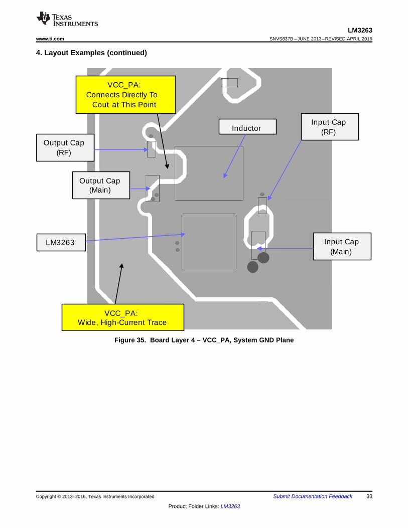
VCC_PA:Connects Directly To
Cout at This Point
Output Cap (RF)
LM3263
Input Cap (RF)Inductor
VCC_PA:Wide, High-Current Trace
Input Cap (Main)
Output Cap (Main)
33
LM3263www.ti.com SNVS837B –JUNE 2013–REVISED APRIL 2016
Product Folder Links: LM3263
Submit Documentation FeedbackCopyright © 2013–2016, Texas Instruments Incorporated
4. Layout Examples (continued)
Figure 35. Board Layer 4 – VCC_PA, System GND Plane

VBATT:Wide,High -Current
Trace
LM3263
Inductor
Output Cap (RF)
Input Cap (RF)
Input Cap (Main)
Output Cap (Main)
34
LM3263SNVS837B –JUNE 2013–REVISED APRIL 2016 www.ti.com
Product Folder Links: LM3263
Submit Documentation Feedback Copyright © 2013–2016, Texas Instruments Incorporated
4. Layout Examples (continued)
Figure 36. Board Layer 5 – VBATT Connection

VBATT Star Connection
VBATT Connection for DC -DC Converter
VBATT BUSConnection for PA(s)
35
LM3263www.ti.com SNVS837B –JUNE 2013–REVISED APRIL 2016
Product Folder Links: LM3263
Submit Documentation FeedbackCopyright © 2013–2016, Texas Instruments Incorporated
4. Layout Examples (continued)
Figure 37. Multiple Board Layers – VBATT Supply Star Connection
10.2.1.1 Star Connection Between VBATT, DC-DC Converter, and PA
10.2.1.1.1 VBATT Star Connection
It is critically important to use a star connection from VBATT supply to the LM3263 PVIN and from VBATT to PAmodules as implementing a daisy-chain supply connection may add noise to the PA output.

PAVBATT
LM3263
PA
VIN DC-DC
VBATT_PA
Star Connection at VBATT
* Proper decoupling on VBATT_PA is strongly recommended.
_
* *
+
VIN
VBATT_PA
Copyright © 2016, Texas Instruments Incorporated
36
LM3263SNVS837B –JUNE 2013–REVISED APRIL 2016 www.ti.com
Product Folder Links: LM3263
Submit Documentation Feedback Copyright © 2013–2016, Texas Instruments Incorporated
4. Layout Examples (continued)
Figure 38. VBATT Star Connection on PCIN and VBATT_PA
10.3 DSBGA Package Assembly and UseUse of the DSBGA package requires specialized board layout, precision mounting, and careful re-flowtechniques, as detailed in AN-1112 DSBGA Wafer Level Chip Scale Package (SNVA009). Refer to the sectionSurface Mount Technology (SMD) Assembly Considerations. For best results in assembly, alignment ordinals onthe PC board must be used to facilitate placement of the device. The pad style used with DSBGA package mustbe the NSMD (non-solder mask defined) type. This means that the solder-mask opening is larger than the padsize. This prevents a lip that otherwise forms if the solder-mask and pad overlap from holding the device off thesurface of the board and interfering with mounting. See SNVA009 for specific instructions how to do this.
The 16-pin package used for the LM3263 has 265 micron (nominal) solder balls and requires 0.225-mm pads formounting the circuit board. The trace to each pad must enter the pad with a 90° entry angle to prevent debrisfrom being caught in deep corners. Initially, the trace to each pad must be about 0.142-mm wide, for a sectionapproximately 0.127-mm long, as a thermal relief. Then each trace must neck up or down to its optimal width.
An important criterion is symmetry to insure the solder bumps on the LM3263 re-flow evenly and that the devicesolders level to the board. In particular, special attention must be paid to the pads for bumps A1, A3, B1, and B3because PGND, PVIN and BGND are typically connected to large copper planes; inadequate thermal relief canresult in inadequate re-flow of these bumps.
The DSBGA package is optimized for the smallest possible size in applications with red-opaque or infrared-opaque cases. Because the DSBGA package lacks the plastic encapsulation characteristic of larger devices, it isvulnerable to light. Backside metallization and/or epoxy coating, along with front-side shading by the printedcircuit board, reduce this sensitivity. However, the package has exposed die edges that are sensitive to light inthe red and infrared range shining on the exposed die edges of the package.

37
LM3263www.ti.com SNVS837B –JUNE 2013–REVISED APRIL 2016
Product Folder Links: LM3263
Submit Documentation FeedbackCopyright © 2013–2016, Texas Instruments Incorporated
11 Device and Documentation Support
11.1 Device Support
11.1.1 Third-Party Products DisclaimerTI'S PUBLICATION OF INFORMATION REGARDING THIRD-PARTY PRODUCTS OR SERVICES DOES NOTCONSTITUTE AN ENDORSEMENT REGARDING THE SUITABILITY OF SUCH PRODUCTS OR SERVICESOR A WARRANTY, REPRESENTATION OR ENDORSEMENT OF SUCH PRODUCTS OR SERVICES, EITHERALONE OR IN COMBINATION WITH ANY TI PRODUCT OR SERVICE.
11.2 Documentation Support
11.2.1 Related DocumentationFor additional information, see the following:
AN-1112 DSBGA Wafer Level Chip Scale Package (SNVA009)
11.3 Community ResourcesThe following links connect to TI community resources. Linked contents are provided "AS IS" by the respectivecontributors. They do not constitute TI specifications and do not necessarily reflect TI's views; see TI's Terms ofUse.
TI E2E™ Online Community TI's Engineer-to-Engineer (E2E) Community. Created to foster collaborationamong engineers. At e2e.ti.com, you can ask questions, share knowledge, explore ideas and helpsolve problems with fellow engineers.
Design Support TI's Design Support Quickly find helpful E2E forums along with design support tools andcontact information for technical support.
11.4 TrademarksE2E is a trademark of Texas Instruments.MIPI is a registered trademark of Mobile Industry Processor Interface Alliance.All other trademarks are the property of their respective owners.
11.5 Electrostatic Discharge CautionThis integrated circuit can be damaged by ESD. Texas Instruments recommends that all integrated circuits be handled withappropriate precautions. Failure to observe proper handling and installation procedures can cause damage.
ESD damage can range from subtle performance degradation to complete device failure. Precision integrated circuits may be moresusceptible to damage because very small parametric changes could cause the device not to meet its published specifications.
11.6 GlossarySLYZ022 — TI Glossary.
This glossary lists and explains terms, acronyms, and definitions.
12 Mechanical, Packaging, and Orderable InformationThe following pages include mechanical, packaging, and orderable information. This information is the mostcurrent data available for the designated devices. This data is subject to change without notice and revision ofthis document. For browser-based versions of this data sheet, refer to the left-hand navigation.

PACKAGE OPTION ADDENDUM
www.ti.com 21-Feb-2016
Addendum-Page 1
PACKAGING INFORMATION
Orderable Device Status(1)
Package Type PackageDrawing
Pins PackageQty
Eco Plan(2)
Lead/Ball Finish(6)
MSL Peak Temp(3)
Op Temp (°C) Device Marking(4/5)
Samples
LM3263TME/NOPB ACTIVE DSBGA YFQ 16 250 Green (RoHS& no Sb/Br)
SNAGCU Level-1-260C-UNLIM -30 to 90 S61
LM3263TMX/NOPB ACTIVE DSBGA YFQ 16 3000 Green (RoHS& no Sb/Br)
SNAGCU Level-1-260C-UNLIM -30 to 90 S61
(1) The marketing status values are defined as follows:ACTIVE: Product device recommended for new designs.LIFEBUY: TI has announced that the device will be discontinued, and a lifetime-buy period is in effect.NRND: Not recommended for new designs. Device is in production to support existing customers, but TI does not recommend using this part in a new design.PREVIEW: Device has been announced but is not in production. Samples may or may not be available.OBSOLETE: TI has discontinued the production of the device.
(2) Eco Plan - The planned eco-friendly classification: Pb-Free (RoHS), Pb-Free (RoHS Exempt), or Green (RoHS & no Sb/Br) - please check http://www.ti.com/productcontent for the latest availabilityinformation and additional product content details.TBD: The Pb-Free/Green conversion plan has not been defined.Pb-Free (RoHS): TI's terms "Lead-Free" or "Pb-Free" mean semiconductor products that are compatible with the current RoHS requirements for all 6 substances, including the requirement thatlead not exceed 0.1% by weight in homogeneous materials. Where designed to be soldered at high temperatures, TI Pb-Free products are suitable for use in specified lead-free processes.Pb-Free (RoHS Exempt): This component has a RoHS exemption for either 1) lead-based flip-chip solder bumps used between the die and package, or 2) lead-based die adhesive used betweenthe die and leadframe. The component is otherwise considered Pb-Free (RoHS compatible) as defined above.Green (RoHS & no Sb/Br): TI defines "Green" to mean Pb-Free (RoHS compatible), and free of Bromine (Br) and Antimony (Sb) based flame retardants (Br or Sb do not exceed 0.1% by weightin homogeneous material)
(3) MSL, Peak Temp. - The Moisture Sensitivity Level rating according to the JEDEC industry standard classifications, and peak solder temperature.
(4) There may be additional marking, which relates to the logo, the lot trace code information, or the environmental category on the device.
(5) Multiple Device Markings will be inside parentheses. Only one Device Marking contained in parentheses and separated by a "~" will appear on a device. If a line is indented then it is a continuationof the previous line and the two combined represent the entire Device Marking for that device.
(6) Lead/Ball Finish - Orderable Devices may have multiple material finish options. Finish options are separated by a vertical ruled line. Lead/Ball Finish values may wrap to two lines if the finishvalue exceeds the maximum column width.
Important Information and Disclaimer:The information provided on this page represents TI's knowledge and belief as of the date that it is provided. TI bases its knowledge and belief on informationprovided by third parties, and makes no representation or warranty as to the accuracy of such information. Efforts are underway to better integrate information from third parties. TI has taken andcontinues to take reasonable steps to provide representative and accurate information but may not have conducted destructive testing or chemical analysis on incoming materials and chemicals.TI and TI suppliers consider certain information to be proprietary, and thus CAS numbers and other limited information may not be available for release.

PACKAGE OPTION ADDENDUM
www.ti.com 21-Feb-2016
Addendum-Page 2
In no event shall TI's liability arising out of such information exceed the total purchase price of the TI part(s) at issue in this document sold by TI to Customer on an annual basis.

TAPE AND REEL INFORMATION
*All dimensions are nominal
Device PackageType
PackageDrawing
Pins SPQ ReelDiameter
(mm)
ReelWidth
W1 (mm)
A0(mm)
B0(mm)
K0(mm)
P1(mm)
W(mm)
Pin1Quadrant
LM3263TME/NOPB DSBGA YFQ 16 250 178.0 8.4 2.08 2.08 0.76 4.0 8.0 Q1
LM3263TMX/NOPB DSBGA YFQ 16 3000 178.0 8.4 2.08 2.08 0.76 4.0 8.0 Q1
PACKAGE MATERIALS INFORMATION
www.ti.com 22-Feb-2016
Pack Materials-Page 1

*All dimensions are nominal
Device Package Type Package Drawing Pins SPQ Length (mm) Width (mm) Height (mm)
LM3263TME/NOPB DSBGA YFQ 16 250 210.0 185.0 35.0
LM3263TMX/NOPB DSBGA YFQ 16 3000 210.0 185.0 35.0
PACKAGE MATERIALS INFORMATION
www.ti.com 22-Feb-2016
Pack Materials-Page 2

MECHANICAL DATA
YFQ0016xxx
www.ti.com
TMD16XXX (Rev A)
E
0.600±0.075
D
A. All linear dimensions are in millimeters. Dimensioning and tolerancing per ASME Y14.5M-1994.B. This drawing is subject to change without notice.
NOTES:
4215081/A 12/12
D: Max =
E: Max =
2.049 mm, Min =
2.049 mm, Min =
1.989 mm
1.989 mm

IMPORTANT NOTICE
Texas Instruments Incorporated (TI) reserves the right to make corrections, enhancements, improvements and other changes to itssemiconductor products and services per JESD46, latest issue, and to discontinue any product or service per JESD48, latest issue. Buyersshould obtain the latest relevant information before placing orders and should verify that such information is current and complete.TI’s published terms of sale for semiconductor products (http://www.ti.com/sc/docs/stdterms.htm) apply to the sale of packaged integratedcircuit products that TI has qualified and released to market. Additional terms may apply to the use or sale of other types of TI products andservices.Reproduction of significant portions of TI information in TI data sheets is permissible only if reproduction is without alteration and isaccompanied by all associated warranties, conditions, limitations, and notices. TI is not responsible or liable for such reproduceddocumentation. Information of third parties may be subject to additional restrictions. Resale of TI products or services with statementsdifferent from or beyond the parameters stated by TI for that product or service voids all express and any implied warranties for theassociated TI product or service and is an unfair and deceptive business practice. TI is not responsible or liable for any such statements.Buyers and others who are developing systems that incorporate TI products (collectively, “Designers”) understand and agree that Designersremain responsible for using their independent analysis, evaluation and judgment in designing their applications and that Designers havefull and exclusive responsibility to assure the safety of Designers' applications and compliance of their applications (and of all TI productsused in or for Designers’ applications) with all applicable regulations, laws and other applicable requirements. Designer represents that, withrespect to their applications, Designer has all the necessary expertise to create and implement safeguards that (1) anticipate dangerousconsequences of failures, (2) monitor failures and their consequences, and (3) lessen the likelihood of failures that might cause harm andtake appropriate actions. Designer agrees that prior to using or distributing any applications that include TI products, Designer willthoroughly test such applications and the functionality of such TI products as used in such applications.TI’s provision of technical, application or other design advice, quality characterization, reliability data or other services or information,including, but not limited to, reference designs and materials relating to evaluation modules, (collectively, “TI Resources”) are intended toassist designers who are developing applications that incorporate TI products; by downloading, accessing or using TI Resources in anyway, Designer (individually or, if Designer is acting on behalf of a company, Designer’s company) agrees to use any particular TI Resourcesolely for this purpose and subject to the terms of this Notice.TI’s provision of TI Resources does not expand or otherwise alter TI’s applicable published warranties or warranty disclaimers for TIproducts, and no additional obligations or liabilities arise from TI providing such TI Resources. TI reserves the right to make corrections,enhancements, improvements and other changes to its TI Resources. TI has not conducted any testing other than that specificallydescribed in the published documentation for a particular TI Resource.Designer is authorized to use, copy and modify any individual TI Resource only in connection with the development of applications thatinclude the TI product(s) identified in such TI Resource. NO OTHER LICENSE, EXPRESS OR IMPLIED, BY ESTOPPEL OR OTHERWISETO ANY OTHER TI INTELLECTUAL PROPERTY RIGHT, AND NO LICENSE TO ANY TECHNOLOGY OR INTELLECTUAL PROPERTYRIGHT OF TI OR ANY THIRD PARTY IS GRANTED HEREIN, including but not limited to any patent right, copyright, mask work right, orother intellectual property right relating to any combination, machine, or process in which TI products or services are used. Informationregarding or referencing third-party products or services does not constitute a license to use such products or services, or a warranty orendorsement thereof. Use of TI Resources may require a license from a third party under the patents or other intellectual property of thethird party, or a license from TI under the patents or other intellectual property of TI.TI RESOURCES ARE PROVIDED “AS IS” AND WITH ALL FAULTS. TI DISCLAIMS ALL OTHER WARRANTIES ORREPRESENTATIONS, EXPRESS OR IMPLIED, REGARDING RESOURCES OR USE THEREOF, INCLUDING BUT NOT LIMITED TOACCURACY OR COMPLETENESS, TITLE, ANY EPIDEMIC FAILURE WARRANTY AND ANY IMPLIED WARRANTIES OFMERCHANTABILITY, FITNESS FOR A PARTICULAR PURPOSE, AND NON-INFRINGEMENT OF ANY THIRD PARTY INTELLECTUALPROPERTY RIGHTS. TI SHALL NOT BE LIABLE FOR AND SHALL NOT DEFEND OR INDEMNIFY DESIGNER AGAINST ANY CLAIM,INCLUDING BUT NOT LIMITED TO ANY INFRINGEMENT CLAIM THAT RELATES TO OR IS BASED ON ANY COMBINATION OFPRODUCTS EVEN IF DESCRIBED IN TI RESOURCES OR OTHERWISE. IN NO EVENT SHALL TI BE LIABLE FOR ANY ACTUAL,DIRECT, SPECIAL, COLLATERAL, INDIRECT, PUNITIVE, INCIDENTAL, CONSEQUENTIAL OR EXEMPLARY DAMAGES INCONNECTION WITH OR ARISING OUT OF TI RESOURCES OR USE THEREOF, AND REGARDLESS OF WHETHER TI HAS BEENADVISED OF THE POSSIBILITY OF SUCH DAMAGES.Unless TI has explicitly designated an individual product as meeting the requirements of a particular industry standard (e.g., ISO/TS 16949and ISO 26262), TI is not responsible for any failure to meet such industry standard requirements.Where TI specifically promotes products as facilitating functional safety or as compliant with industry functional safety standards, suchproducts are intended to help enable customers to design and create their own applications that meet applicable functional safety standardsand requirements. Using products in an application does not by itself establish any safety features in the application. Designers mustensure compliance with safety-related requirements and standards applicable to their applications. Designer may not use any TI products inlife-critical medical equipment unless authorized officers of the parties have executed a special contract specifically governing such use.Life-critical medical equipment is medical equipment where failure of such equipment would cause serious bodily injury or death (e.g., lifesupport, pacemakers, defibrillators, heart pumps, neurostimulators, and implantables). Such equipment includes, without limitation, allmedical devices identified by the U.S. Food and Drug Administration as Class III devices and equivalent classifications outside the U.S.TI may expressly designate certain products as completing a particular qualification (e.g., Q100, Military Grade, or Enhanced Product).Designers agree that it has the necessary expertise to select the product with the appropriate qualification designation for their applicationsand that proper product selection is at Designers’ own risk. Designers are solely responsible for compliance with all legal and regulatoryrequirements in connection with such selection.Designer will fully indemnify TI and its representatives against any damages, costs, losses, and/or liabilities arising out of Designer’s non-compliance with the terms and provisions of this Notice.
Mailing Address: Texas Instruments, Post Office Box 655303, Dallas, Texas 75265Copyright © 2017, Texas Instruments Incorporated