low power design in cmos - university of california,...
TRANSCRIPT

Digital Integrated Circuits © Prentice Hall 1995Low Power DesignLow Power Design
Low Power Design in CMOS
Digital Integrated Circuits © Prentice Hall 1995Low Power DesignLow Power Design
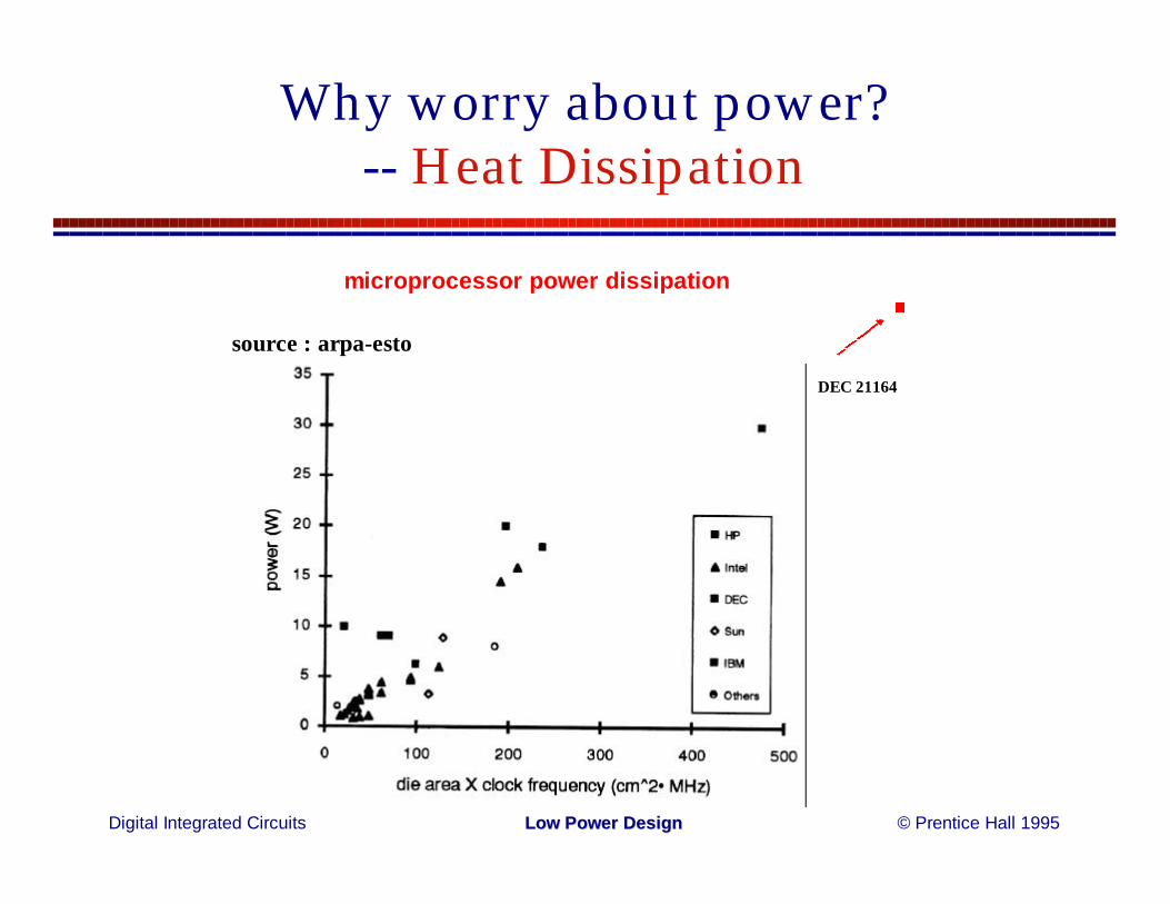
Why worry about power?-- Heat Dissipation
DEC 21164
source : arpa-esto
microprocessor power dissipation

Digital Integrated Circuits © Prentice Hall 1995Low Power DesignLow Power Design
Evolution in Power Dissipation

Digital Integrated Circuits © Prentice Hall 1995Low Power DesignLow Power Design
Why worry about power —Portability
Multimedia Terminals
Laptop Computers
Digital Cellular Telephony
BATTERY(40+ lbs)
Year
Nom
inal
Cap
acity
(Wat
t-hou
rs /
lb)
Nickel-Cadium
Ni-Metal Hydride
65 70 75 80 85 90 95 0
10
20
30
40
50 Rechargable Lithium
Expected Battery Lifetime increaseover next 5 years: 30-40%

Digital Integrated Circuits © Prentice Hall 1995Low Power DesignLow Power Design
Where Does Power Go in CMOS?
• Dynamic Power Consumption
• Short Circuit Currents
• Leakage
Charging and Discharging Capacitors
Short Circuit Path between Supply Rails during Switching
Leaking diodes and transistors

Digital Integrated Circuits © Prentice Hall 1995Low Power DesignLow Power Design
Dynamic Power Consumption
V i n V out
C L
Energy/transit ion = CL * V d d2
Power = Energy/transit ion * f = C L * V dd2 * f
Need to reduce C L , V dd , and f to reduce power.
Vdd
Not a function of transistor sizes!

Digital Integrated Circuits © Prentice Hall 1995Low Power DesignLow Power Design
Dynamic Power Consumption - Revisited
Power = Energy/transition * transition rate
= CL * Vdd2 * f0→ 1
= CL * Vdd2 * P0→ 1* f
= CEFF * Vdd2 * f
Power Dissipation is Data DependentFunction of Switching Activity
CEFF = Effective Capacitance = CL * P0→ 1

Digital Integrated Circuits © Prentice Hall 1995Low Power DesignLow Power Design
Power Consumption is Data Dependent
Example: Static 2 Input NOR Gate
Assume:P(A=1) = 1/2P(B=1) = 1/2
P(Out=1) = 1/4P(0→ 1)
= 3/4 × 1/4 = 3/16
Then:
= P(Out=0).P(Out=1)
CEFF = 3/16 * CL

Digital Integrated Circuits © Prentice Hall 1995Low Power DesignLow Power Design
Transition Probabilities for Basic Gates

Digital Integrated Circuits © Prentice Hall 1995Low Power DesignLow Power Design
Transition Probability of 2-input NOR Gate

Digital Integrated Circuits © Prentice Hall 1995Low Power DesignLow Power Design
Problem: Reconvergent Fanout
A
B
X
Z
Reconvergence
P(Z=1) = P(B=1) . P(X=1 | B=1)
Becomes complex and intractable real fast

Digital Integrated Circuits © Prentice Hall 1995Low Power DesignLow Power Design
How about Dynamic Circuits?
Mp
Me
VDD
PDN
φ
In1In2In3
Out
φ
Power is Only Dissipated when Out=0!
CEFF = P(Out=0).CL

Digital Integrated Circuits © Prentice Hall 1995Low Power DesignLow Power Design
4-input NAND Gate
Example: Dynamic 2 Input NOR Gate
Assume:P(A=1) = 1/2P(B=1) = 1/2
P(Out=0) = 3/4
Then:
CEFF = 3/4 * CL
Switching Activity Is Always Higher in Dynamic Circuits

Digital Integrated Circuits © Prentice Hall 1995Low Power DesignLow Power Design
Transition Probabilities for Dynamic Gates
Switching Activity for Precharged Dynamic Gates
P0→ 1 = P0

Digital Integrated Circuits © Prentice Hall 1995Low Power DesignLow Power Design
Glitching in Static CMOS
A
B
X
CZ
ABC 101 000
X
Z
Unit Delay
also called: dynamic hazards
Observe: No glitching in dynamic circuits
Digital Integrated Circuits © Prentice Hall 1995Low Power DesignLow Power Design
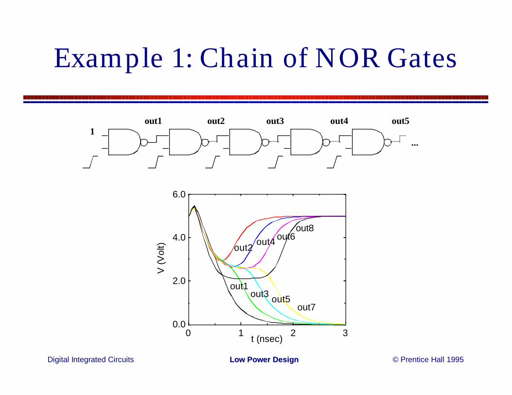
Example 1: Chain of NOR Gates
0 1 2 3t (nsec)0.0
2.0
4.0
6.0
V (V
olt)
out1out3 out5
out7
out2 out4 out6out8
1out1 out2 out3 out4 out5
...
Digital Integrated Circuits © Prentice Hall 1995Low Power DesignLow Power Design
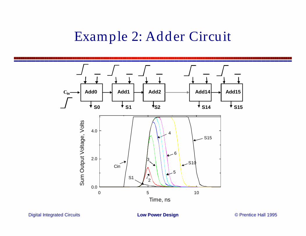
Example 2: Adder Circuit
0 5 100.0
2.0
4.0
Time, ns
Sum
Out
put V
olta
ge, V
olts
Cin
S15
S10
6
5
4
3
2S1
Add0 Add1 Add2 Add14 Add15
S0 S1 S2 S14 S15
Cin
Digital Integrated Circuits © Prentice Hall 1995Low Power DesignLow Power Design
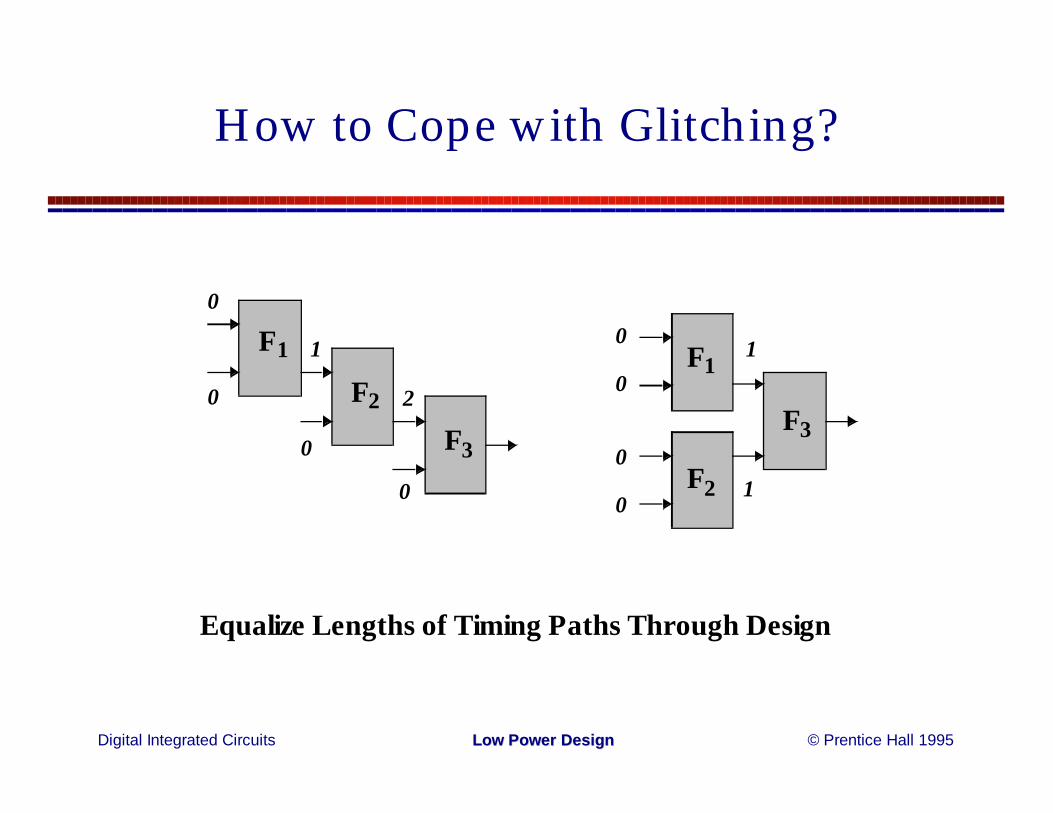
How to Cope with Glitching?
F1
F2
F3
F1
F3
F2
0
0
0
0
1
2
0
0
0
0 1
1
Equalize Lengths of Timing Paths Through Design

Digital Integrated Circuits © Prentice Hall 1995Low Power DesignLow Power Design
Short Circuit Currents
Vin Vout
CL
Vdd
I VD
D (m
A)
0.15
0.10
0.05
Vin (V)5.04.03.02.01.00.0

Digital Integrated Circuits © Prentice Hall 1995Low Power DesignLow Power Design
Impact of rise/fall times on short-circuitcurrents
VDD
Vout
CL
Vin
ISC ≈ 0
VDD
Vout
CL
Vin
ISC ≈ IMAX
Large capacitive load Small capacitive load

Digital Integrated Circuits © Prentice Hall 1995Low Power DesignLow Power Design
Short-circuit energy as a function of sloperatio
0r
876543210
1 2 3 4 5
∆E / E
VDD = 5 V
VDD = 3.3 V
W/L|P = 7.2µm/1.2µm W/L|N = 2.4µm/1.2µm
The power dissipation due to short circuit currents is
rise/fall times of the input and output signals.
minimized by matching the

Digital Integrated Circuits © Prentice Hall 1995Low Power DesignLow Power Design
Static Power Consumption
V in=5V
Vout
CL
Vdd
Istat
Pstat = P(In=1).Vdd . Istat
• Dominates over dynamic consumption
• Not a function of switching frequency
Digital Integrated Circuits © Prentice Hall 1995Low Power DesignLow Power Design
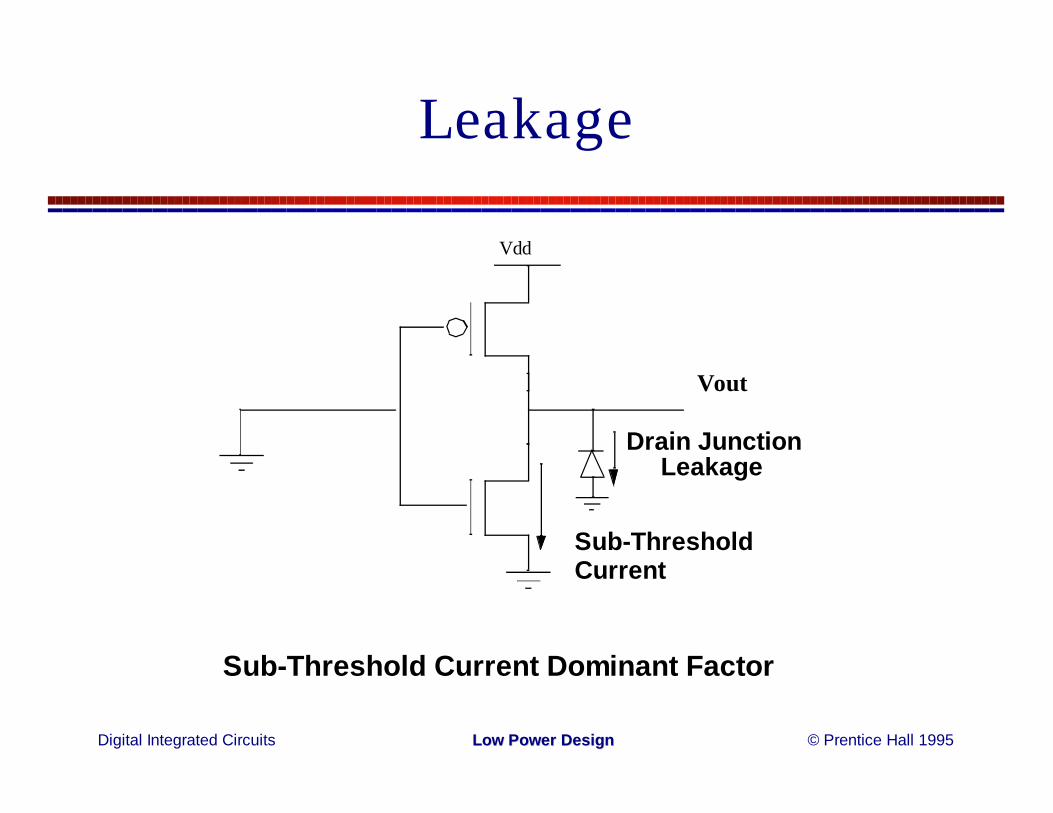
Leakage
Vout
Vdd
Sub-ThresholdCurrent
Drain JunctionLeakage
Sub-Threshold Current Dominant Factor

Digital Integrated Circuits © Prentice Hall 1995Low Power DesignLow Power Design
Sub-Threshold in MOS
VT=0.6VT=0.2
√ID
VGS
Lower Bound on Threshold to Prevent Leakage

Digital Integrated Circuits © Prentice Hall 1995Low Power DesignLow Power Design
Power Analysis in SPICE
RCk iDDCircuit
Under Test
+
-
VDD
iDD
Pav
Equivalent Circuit for Measuring Power in SPICE

Digital Integrated Circuits © Prentice Hall 1995Low Power DesignLow Power Design
Design for Worst Case
VDD
CL
F
A
A B
B
2
2
1 1
VDD
AB
C
D
DA
B C
12
22
2
24
4
F
Here it is assumed that Rp = Rn

Digital Integrated Circuits © Prentice Hall 1995Low Power DesignLow Power Design
Reducing Vdd
P x td = Et = CL * Vdd2
E(Vdd=2)=
(CL) * (2)2
(CL) * (5)2E(Vdd=5)
Strong function of voltage (V2 dependence).
Relatively independent of logic function and style.
E(Vdd=2) ≈ 0.16 E(Vdd =5)
0.03
0.05
0.07
0.1
0.15
0.20
0.30
0.50
0.70
1.00
1.5
1 2 5
51 stage ring oscillator
8-bit adder
Vdd (volts)
quadratic dependence
NO
RM
ALI
ZED
PO
WE
R-D
EL
AY
PR
OD
UC
T
Power Delay Product Improves with lowering VDD.

Digital Integrated Circuits © Prentice Hall 1995Low Power DesignLow Power Design
Lower Vdd Increases Delay
CL * Vdd
I=Td
Td(Vdd=5)
Td(Vdd=2)=
(2) * (5 - 0.7)2
(5) * (2 - 0.7)2
≈ 4
I ~ (Vdd - Vt)2
Relatively independent of logic function and style.
1.001.502.002.503.003.504.004.505.005.506.006.507.007.50
2.00 4.00 6.00Vdd (volts)
NO
RM
AL
IZED
DE
LA
Y
adder (SPICE)
microcoded DSP chip
multiplier
adder
ring oscillator
clock generator2.0µm technology

Digital Integrated Circuits © Prentice Hall 1995Low Power DesignLow Power Design
Lowering the Threshold
DESIGN FOR PLeakage == PDynamic
Vt = 0.2Vt = 0
ID
VGS
Reduces the Speed Loss, But Increases Leakage
Vdd
Delay
2Vt
Interesting Design Approach:

Digital Integrated Circuits © Prentice Hall 1995Low Power DesignLow Power Design
Transistor Sizing for Power Minimization
Minimum sized devices are usually optimal for low-power.
Small W/L’s
Large W/L’s
Higher Voltage
Lower Voltage
Lower Capacitance
Higher Capacitance
Larger sized devices are useful only when interconnect dominated.

Digital Integrated Circuits © Prentice Hall 1995Low Power DesignLow Power Design
Transistor Sizing for Fixed Throughput
α = 0
adder
0.5
0.7
1.0
1.52
345
7
10
1 3 10
α = 0.5
α = 1
α = 1.5
α = 2
W/L
NO
RM
ALI
ZE
D E
NE
RG
Y
CP = Cwiring + CDF
Cg = W/L CMIN I ∝ W/L CMIN
CMIN = Minimum sized gate (W/L=1) W /L after sizing
HIGH PERFORMANCE
W/L >> CP / (K CMIN)
LOW POWER
W/L = 2 CP / (K CMIN) (if CP ≥ K CMIN)
W/L = 1 ELSE
α = CP / (K CMIN)

Digital Integrated Circuits © Prentice Hall 1995Low Power DesignLow Power Design
Reducing Effective Capacitance
Global bus architecture Local bus architecture
Shared Resources incur Switching Overhead
Digital Integrated Circuits © Prentice Hall 1995Low Power DesignLow Power Design
Summary
• Power Dissipation is becoming Prime DesignConstraint
• Low Power Design requires Optimization at all Levels
• Sources of Power Dissipation are well characterized
• Low Power Design requires operation at lowest possible voltage and clock speed