low-voltage cmos temperature sensor …cmosedu.com/jbaker/students/theses/low-voltage cmos...
TRANSCRIPT
LOW-VOLTAGE CMOS TEMPERATURE SENSOR DESIGN
USING SCHOTTKY DIODE-BASED REFERENCES
By
Curtis Wayne Cahoon
A thesis
submitted in partial fulfillment
of the requirements for the degree of
Master of Science in Electrical Engineering
Boise State University
June, 2008

ii
APPROVAL TO SUBMIT THESIS
The thesis presented by Curtis Wayne Cahoon entitled LOW-VOLTAGE CMOS
TEMPERATURE SENSOR DESIGN USING SCHOTTKY DIODE-BASED
REFERENCES is hereby approved:
R. Jacob Baker Date
Advisor
Wan Kuang Date
Committee Member
Scott Smith Date
Committee Member
John R. (Jack) Pelton Date
Dean of the Graduate College

iii
DEDICATION
This thesis is dedicated to my wonderful family, especially my wife Sara, my
parents, and my brother and sister. Without their constant encouragement and patience
with me throughout the duration of this project, its completion would not have been
possible.

iv
ACKNOWLEDGEMENTS
I would like to take this opportunity to express my heartfelt gratitude to Dr. Jake
Baker for his guidance, and instruction that he has given me from the time I took my first
class from him as an undergraduate through the completion of my Master’s degree. The
skills I have been able to learn from him have already benefitted me immensely and will
continue to be a great benefit to me throughout my future endeavors, both academically
and professionally. I have definitely been challenged in my education and have grown
from it both as a person and as an engineer. I also would like to thank him for the
friendship he has offered through my entire time at Boise State University.
I also would like to thank Micron Technology for providing me with a job that
has enabled me to learn many new skills that will be a great benefit to me throughout my
career. I also would like to thank them for funding nearly my entire graduate education.
Thanks go out to Frank Ross (my first engineering manager at Micron), Sugato
Mukherjee, Ben Millemon, Aaron Erbe, and Dave Butler for enduring my constant
questions and offering valuable feedback through the phases of this project.
Finally, I would like to thank my wonderful wife Sara. She has been an
inspiration in the way she overcomes every challenge in her life, even though they may
seem impossible at times. I would not have accomplished much without her love,
friendship, and constant encouragement. Thank you for all of your love and patience.
v
AUTOBIOGRAPHICAL SKETCH
Curtis Wayne Cahoon was born in Glenwood Springs, Colorado, on June 23,
1978. He received a B.S. in electrical engineering from Boise State University in May,
2002 and is currently completing the final requirements for an M.S.E.E. degree from
Boise State University.
As an undergraduate, he was a math tutor and teaching assistant for the Electrical
Engineering department at Boise State University. He also performed research exploring
the effects of high frequency noise on integrated circuits, exploring the use of sigma-delta
modulation in conjunction with RF power detectors for noise measurement in CMOS
integrated circuits.
Upon graduation from Boise State in 2002, Curtis started work for Micron
Technology where he is currently a Database Design Engineer, aiding in the debug and
design verification of various DRAM memory products. His work with Micron has
included working on the design and product development of embedded DRAM,
Reduced-Latency DRAM (RLDRAM), mobile DRAM, and DDR3 memory products.
vi
ABSTRACT
Thermal management circuits have been used for many years in systems such as
air conditioners, ovens, and engines. Today temperature sensors are often integrated onto
the same chip as microprocessors, memory circuits, and other ICs to help control system
temperature. In most commonly-used integrated CMOS temperature sensors, bias circuits
that utilize a PN junction diode (or diode-connected PNP bipolar transistor) are used.
This is due to the well-defined I-V temperature characteristics of the semiconductor PN
junction. The forward bias voltage of this junction is approximately 0.7 V.
As CMOS device geometries continue to shrink, so does the supply voltage. As
the supply voltage decreases, this 0.7 V drop can be a limiting factor. The need for a
device with a similar well-defined temperature characteristic and a lower forward-bias
voltage becomes obvious. The design of a temperature sensor using the Schottky metal-
semiconductor (MS) junction diode as a replacement for the tradition PN junction diode
is presented in this work. The voltage required to forward-bias a Schottky diode is
approximately half that of a PN junction diode, which allows for lower voltage operation.
This research explores various temperature sensor topologies used for low-voltage
temperature sensing. The topology used for the finished product is that of a fully
differential sigma-delta temperature sensor. This topology was chosen for its excellent
noise performance and good low-voltage operation. This sensor was designed and
fabricated using the AMI 0.5um process through the MOSIS fabrication organization.
The chip performance has been evaluated and compared to the simulated results to verify
vii
accurate low voltage operation over a wide temperature range. The final design achieves
an effective resolution of 0.7 ˚C and consumes an average current of less than 1 µA at a
rate of 20 temperature readings per second. Silicon results also confirmed that the fully
differential sigma-delta sensor also shows better noise performance than a similar single-
ended sigma-delta sensor. The Schottky-based current references used in the sensor
achieve over 300 mV of additional low-voltage margin when compared to PN junction
diode-based current references.

viii
TABLE OF CONTENTS
APPROVAL TO SUBMIT THESIS .................................................................................. ii
DEDICATION ................................................................................................................... iii
ACKNOWLEDGEMENTS ............................................................................................... iv
AUTOBIOGRAPHICAL SKETCH ................................................................................... v
ABSTRACT ....................................................................................................................... vi
TABLE OF CONTENTS ................................................................................................. viii
FIGURES AND TABLES .................................................................................................. x
LIST OF ABBREVIATIONS .......................................................................................... xvi
CHAPTER 1 – INTRODUCTION ..................................................................................... 1
1.1 Motivation ................................................................................................................. 1
1.2 Temperature Sensing Basics ..................................................................................... 3
1.3 Thesis Organization ................................................................................................... 8
CHAPTER 2 – TEMPERATURE SENSOR TOPOLOGIES ............................................ 9
2.1 Flash and Successive Approximation ADCs ............................................................ 9
2.2 A Novel Approach – Time-to-Digital Conversion .................................................. 12
2.3 Sigma-Delta ADC-based Temperature Sensing ...................................................... 22
CHAPTER 3 – SCHOTTKY DIODES ............................................................................ 29
3.1 Standard PN Junction Diode Review ..................................................................... 29
3.2 Semiconductor Diode SPICE Model ....................................................................... 30
3.3 Schottky Diode Theory ........................................................................................... 34
CHAPTER 4 – CURRENT REFERENCES AND CURRENT MIRRORING ............... 39
4.1 Introduction ............................................................................................................. 39
ix
4.2 Review of CMOS Current Reference Design ......................................................... 40
4.3 Accuracy Issues in Current Reference Design ........................................................ 46
4.4 Accurate Current Mirroring..................................................................................... 51
CHAPTER 5 – FULLY DIFFERENTIAL SIGMA-DELTA TEMPERATURE SENSOR
............................................................................................................................... 54
5.1 Introduction ............................................................................................................. 54
5.2 Temperature Sensitive Current References ............................................................. 54
5.3 Data Converter Design ............................................................................................ 57
5.4 Mixed-Signal Design Issues .................................................................................... 70
5.5 Simulation Results ................................................................................................... 73
5.6 Summary ................................................................................................................. 77
CHAPTER 6 – TEST CHIP RESULTS ........................................................................... 78
6.1 Diode Characterization ............................................................................................ 78
6.2 Current Source Characterization ............................................................................. 81
6.3 Temperature Sensor characterization ...................................................................... 82
CHAPTER 7 – CONCLUSIONS AND FUTURE WORK .............................................. 92
7.1 Conclusions ............................................................................................................. 92
7.2 Future Work ............................................................................................................ 93
WORKS CITED ............................................................................................................... 95
APPENDIX A ................................................................................................................... 97
Diode I-V Curves Measured from Diode Test Structures ............................................. 97
APPENDIX B ................................................................................................................. 100
Key Temperature Sensor Schematics .......................................................................... 100

x
FIGURES AND TABLES
Figure 1.1 Topdown view of a parasitic diode-connected PNP transistor in a typical
CMOS process. ....................................................................................................... 4
Figure 1.2 Cross-sectional view of the parasitic diode-connected PNP transistor in a
typical CMOS process. ........................................................................................... 4
Figure 1.3 An example of a PTAT current source in a CMOS process (startup circuit not
shown). .................................................................................................................... 6
Figure 1.4 Block diagram illustrating the conversion process in a CMOS smart
temperature sensor. ................................................................................................. 7
Figure 2.1 Voltage vs. Temperature curves illustrating operation of a 2-bit Flash-type
temperature sensor. ............................................................................................... 10
Figure 2.2 Diagram of a Flash ADC-based temperature sensor having temperature curves
illustrated in Fig. 2.1. ............................................................................................ 10
Figure 2.3 Operation of a Time-to-Digital Converter-Based Temperature Sensor. ......... 14
Figure 2.4 Schematic diagram of PTAT pulse generator used in TDC-based temperature
sensor. Temperature-insensitive delay line added for DC offset removal. ........... 14
Figure 2.5 Graphs illustrating the removal of DC offset from PTAT pulse generator. .... 15
Figure 2.6 Current-starved inverter-based delay element for use in a TDC-based
temperature sensor ................................................................................................ 16
Figure 2.7 Schematic of a TDC-based temperature sensor designed in [5]...................... 17
Figure 2.8 Current-starved inverter with biasing for better temperature insensitivity. .... 18
xi
Figure 2.9 PTAT (left) and CTAT current references used for biasing voltage-controlled
delay lines in a TDC-based temperature sensor. Schottky diodes are used to
improve low-voltage operation of the references. ................................................ 19
Figure 2.10 Simulation results of a 68-stage inverter-based delay line using the AMI
0.5um process showing .. approximately linear operation across temperature range
of -55˚C to 125˚C. ................................................................................................. 20
Figure 2.11 Fully differential voltage-controlled delay element for use in the delay lines
of the TDC-based temperature sensor. Biasing voltages generated with biasing
circuits derived from Fig. 2.9, but not shown here (for simplicity). ..................... 21
Figure 2.12 Block diagram of a first-order sigma-delta modulator (ADC). ..................... 23
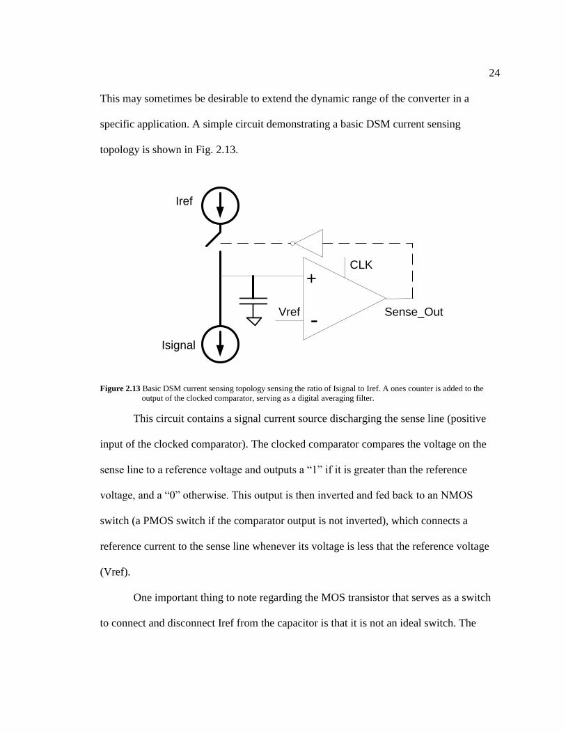
Figure 2.13 Basic DSM current sensing topology sensing the ratio of Isignal to Iref. A
ones counter is added to the output of the clocked comparator, serving as a digital
averaging filter. ..................................................................................................... 24
Figure 3.1 Diode-Connected PNP transistor (Schematic View). ...................................... 29
Figure 3.2 Band diagram illustrating a PN junction and how it forms a built-in potential at
the junction............................................................................................................ 31
Table 3.1 Model parameters and their default values for the Berkeley semiconductor
diode SPICE model. .............................................................................................. 33
Figure 3.3 Band diagram of a metal-semiconductor junction showing the formation of a
Schottky barrier at the junction. ............................................................................ 35
Figure 3.4 Layout view of a Schottky diode in a typical CMOS process. ........................ 37
xii
Figure 3.5 Cross-sectional diagram and Schottky diode symbol used in a CMOS process.
............................................................................................................................... 37
Figure 4.1 Beta Multiplier Reference Circuit used in a short-channel CMOS process. ... 40
Figure 4.2 CTAT current reference using a Schottky diode. ............................................ 42
Figure 4.3 Schematic of a CMOS PTAT current reference using Schottky diodes. ........ 44
Figure 4.4 Graph of PTAT current across an unreasonably wide temperature range to see
effect of non-linear temperature slope. ................................................................. 46
Table 4.1 Values for three different diode SPICE models showing very similar forward
bias characteristics. ............................................................................................... 47
Table 4.2 Simulation results for PTAT current source with 3 different diode models. .... 48
Figure 4.5 PTAT Current vs. temperature showing effect of diff amp offset. ................. 49
Figure 4.6 CTAT current vs. temperature showing effect of diff amp offset. .................. 50
Figure 4.7 General cascode current biasing circuit for sourcing and sinking reference
currents. ................................................................................................................. 52
Figure 4.8 Regulated drain NMOS current mirror............................................................ 53
Figure 5.1 PTAT currents vs. supply voltage for PN diode and Schottky diode-based
references. ............................................................................................................. 55
Figure 5.2 CTAT currents vs. supply voltage for PN and Schottky diode-based
references. ............................................................................................................. 55
Figure 5.3 Modified DSM topology to eliminate current design restrictions. .................. 58
Figure 5.4 Graph of DSM output code vs. temperature in conventional current sensing
configuration. ........................................................................................................ 60
xiii
Figure 5.5 Modified DSM temperature sensing topology that increases temperature
sensor resolution (dynamic range). ....................................................................... 61
Figure 5.6 Temperature graph showing 3X increase in temperature resolution with
modified DSM topology. ...................................................................................... 63
Figure 5.7 Comparator input waveforms in a single-ended DSM topology. .................... 64
Figure 5.8 Fully differential version of the Kelvin-to-Celsius (extended range) topology.
............................................................................................................................... 65
Figure 5.9 Common-mode drift caused by current source/sink mismatch. ...................... 66
Figure 5.10 Common-mode feedback (CMFB) amplifier used to keep Vcm at VREF. .. 66
Figure 5.11 Comparator inputs in differential DSM topology with addition of CMFB
amplifier. ............................................................................................................... 67
Figure 5.12 Common-mode voltage after the addition of the CMFB amplifier. .............. 68
Figure 5.13 Full-chip layout of the temperature sensor test chip. .................................... 71
Table 5.1 Power supply domains used to improve noise performance. ............................ 72
Figure 5.14 Diagram showing the common centroid concept for improved element
matching. ............................................................................................................... 73
Figure 5.15 Transfer curve with no mismatch and an example of how calibration works
by simply subtracting the count at the -40˚C calibration point (setting -40˚C equal
to a count of zero). ................................................................................................ 74
Figure 5.16 Simulation results with perfectly matched currents and a simulation with a
mismatch of ~2% in both ICTAT and IPTAT. ..................................................... 74
xiv
Figure 5.17 Graph showing gain variation of up to 5.5% with variation in offset voltage
of differential amplifiers. ...................................................................................... 75
Figure 6.1 Photo of chip (inside packaging). .................................................................... 78
Figure 6.2 Zoomed in view of Schottky test structures (with anode and cathode labeled).
............................................................................................................................... 79
Figure 6.3 HP 4156C Semiconductor Parametric Analyzer used for Schottky diode
characterization. .................................................................................................... 80
Figure 6.4 Pinout diagram for the temperature sensor test chip. ...................................... 83
Table 6.1 Pin list for Temp Sensor test chip. .................................................................... 84
Figure 6.5 Test board for characterizing the DSM temperature sensor. ........................... 86
Figure 6.6 Test setup for DSM sensor validation. ............................................................ 87
Figure 6.7 Temperature chamber used for testing DSM temperature sensors. ................. 88
Figure 6.8 Temperature data for differential and single-ended DSM temperature sensors.
............................................................................................................................... 89
Figure A.1 I-V curves for a single diode test structure on all five chips. ......................... 98
Figure A.2 I-V curves for parallel 2-diode test structure. ................................................. 98
Figure A.3 I-V curves for 4-diode parallel test structure. ................................................. 99
Figure A.4 I-V curves for 8-diode parallel test structure. ................................................. 99
Figure B.1 Fullchip schematic of differential DSM sensor. ........................................... 101
Figure B.2 Schematic of clocked comparator with PMOS pre-amplifier and reset logic.
............................................................................................................................. 101
Figure B.3 Common mode feedback (CMFB) amplifier schematic. .............................. 102

xv
Figure B.4 Ones counter (digital averaging filter) schematic. Notice CLK is inverted to
prevent setup time violation. ............................................................................... 102
xvi
LIST OF ABBREVIATIONS
ADC Analog-to-Digital Converter
BMR Beta Multiplier Reference
CMOS Complementary Metal-Oxide Semiconductor
CTAT Complementary to Absolute Temperature
DAC Digital-to-Analog Converter
DSM Delta-Sigma (or Sigma-Delta) Modulator
PTAT Proportional to Absolute Temperature
SPA Semiconductor Parametric Analyzer
SPICE Simulation Program with Integrated Circuit Emphasis
TDC Time-to-Digital Converter
VCDL Voltage-Controlled Delay Line
1
CHAPTER 1 – INTRODUCTION
1.1 Motivation
Major advances in microelectronics technology and an explosion in the demand
for portable/mobile electronic systems have driven semiconductor manufacturers to
aggressively scale down CMOS device dimensions. This is necessary to maximize
computing power per square unit of silicon and also to drive manufacturing costs down
by maximizing die-per-wafer for a given product.
As CMOS process geometries shrink, voltage supply levels are also reduced,
which has the benefit of power reduction, especially for digital systems. However, as the
supply voltages are reduced, many challenges arise in the area of analog design. Even in
systems that are considered almost exclusively digital, such as microprocessors and
memory (Flash, DRAM), there are a number of analog and mixed-signal circuits that are
necessary for good system performance. Some problems introduced by the reduction in
CMOS device feature size include decreased transistor gain, lower dynamic range, and
poorer noise margins [1].
An important issue for powerful, high-speed computing systems (containing
microprocessor cores and high speed DRAM) is thermal management. This is of special
concern with laptops, PDAs, and other portable computing devices where the heat sinks
and/or fans can only help dissipate the heat to a limited degree. This makes variations in
clock frequency and/or variation in modes of device operation for DRAM, Flash, and
2
other systems necessary. On-chip smart CMOS temperature sensors have been commonly
used for thermal management in these applications [2].
The motivation for this research is a combination of the two previously mentioned
issues. As operating voltages approach the sub-1V range, it becomes increasingly
difficult (and eventually impossible) to design a good precision voltage or current
reference with well-defined temperature characteristics. This is due to the inherent
voltage drop (approximately 0.65-0.7 V) across the junction of a PN junction diode used
in such a reference (PN junction diodes are compatible with almost any CMOS process).
Since such a reference is very important in a high-resolution temperature sensor, a
solution to significantly lower the minimum operating voltage of the current/voltage
source used in CMOS temperature sensors is needed. This research explores using
Schottky diodes to bias these references and serve as a solution to this problem.
Also in low-voltage systems with analog/mixed-signal components, it becomes a
serious challenge to perform high-resolution data conversion due to the reduced transistor
gains and inherently lower dynamic range. A number of different data converter
architectures have been explored to attempt to overcome the challenges introduced by
lower operating voltages. Some of the methods discussed in this paper include time-to-
digital conversion, sigma-delta noise-shaping data conversion, and fully differential
sensing. The architecture used in the final design is that of a fully differential current
mode sigma-delta modulator.

3
Other important issues in temperature sensor design include manufacturability,
low-voltage operation, power consumption, cost, and testability. A temperature sensor
integrated into a memory system or other such device should have minimal impact on the
power budget and have minimal impact on test time and cost. Special attention was given
to these issues in the design of this sensor. The sensor was designed to draw less than 1
µA average current and to achieve good accuracy with a single-point temperature
calibration. A single-point temperature calibration minimizes the additional test time
required by the temperature sensor (and therefore has a minimal impact on the test cost).
1.2 Temperature Sensing Basics
Integrated CMOS smart temperature sensors are a family of temperature sensors
that are widely used in many different commercial applications today [2]. These sensors
have almost exclusively used the parasitic bipolar transistor that is inherent in CMOS
processes. Normally, the parasitic device is not desirable in the process, but it can be
taken advantage of to make precision voltage and current references, and also to make
integrated smart temperature sensors.
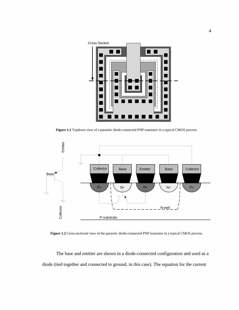
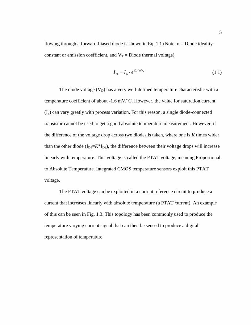
Consider the diagrams below showing top-down and cross-sectional views of the
parasitic bipolar junction transistor:
4
C
C
C
C
C
CC
CC
Cross Section
Figure 1.1 Topdown view of a parasitic diode-connected PNP transistor in a typical CMOS process.
P-substrate
N-well
P+ P+ P+N+ N+
EmitterBase Collector
Em
itte
r
Base
Co
llecto
r
BaseCollector
Figure 1.2 Cross-sectional view of the parasitic diode-connected PNP transistor in a typical CMOS process.
The base and emitter are shown in a diode-connected configuration and used as a
diode (tied together and connected to ground, in this case). The equation for the current
5
flowing through a forward-biased diode is shown in Eq. 1.1 (Note: n = Diode ideality
constant or emission coefficient, and VT = Diode thermal voltage).
TD VnV
SD eII
/ (1.1)
The diode voltage (VD) has a very well-defined temperature characteristic with a
temperature coefficient of about -1.6 mV/˚C. However, the value for saturation current
(IS) can vary greatly with process variation. For this reason, a single diode-connected
transistor cannot be used to get a good absolute temperature measurement. However, if
the difference of the voltage drop across two diodes is taken, where one is K times wider
than the other diode (ID1=K*ID2), the difference between their voltage drops will increase
linearly with temperature. This voltage is called the PTAT voltage, meaning Proportional
to Absolute Temperature. Integrated CMOS temperature sensors exploit this PTAT
voltage.
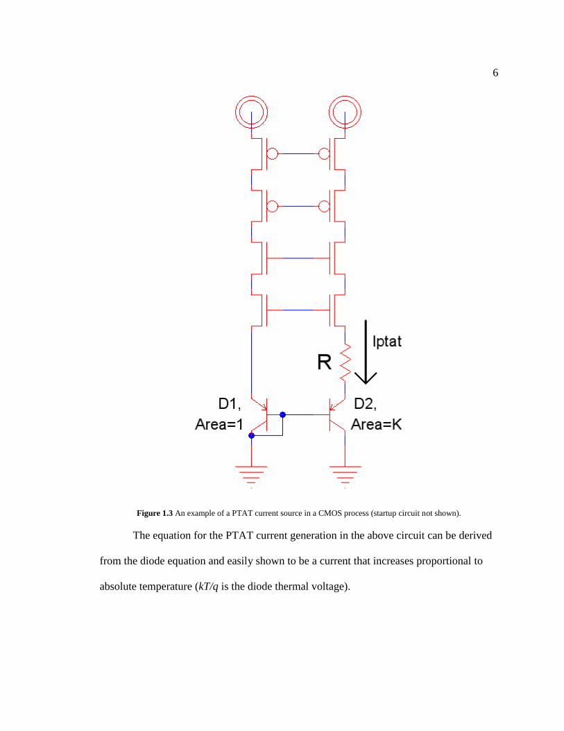
The PTAT voltage can be exploited in a current reference circuit to produce a
current that increases linearly with absolute temperature (a PTAT current). An example
of this can be seen in Fig. 1.3. This topology has been commonly used to produce the
temperature varying current signal that can then be sensed to produce a digital
representation of temperature.
6
Figure 1.3 An example of a PTAT current source in a CMOS process (startup circuit not shown).
The equation for the PTAT current generation in the above circuit can be derived
from the diode equation and easily shown to be a current that increases proportional to
absolute temperature (kT/q is the diode thermal voltage).
7
TqR
KknI PTAT
ln (1.2)
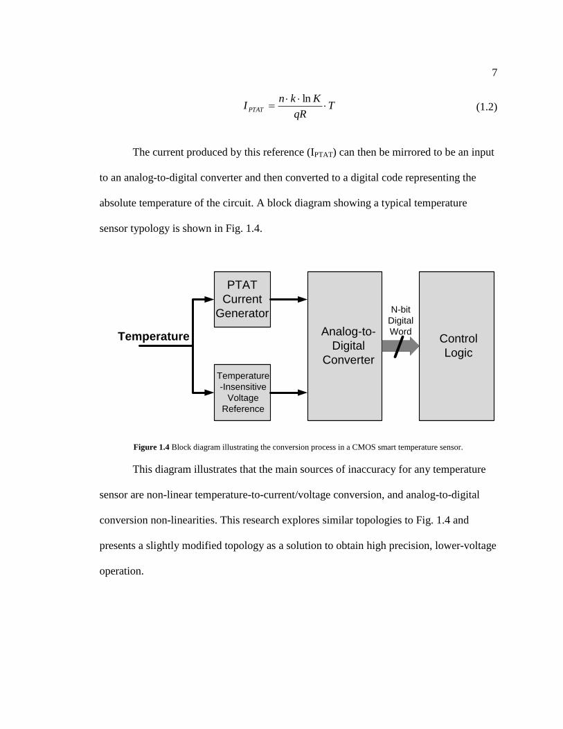
The current produced by this reference (IPTAT) can then be mirrored to be an input
to an analog-to-digital converter and then converted to a digital code representing the
absolute temperature of the circuit. A block diagram showing a typical temperature
sensor typology is shown in Fig. 1.4.
Temperature
N-bit
Digital
WordControl
Logic
Analog-to-
Digital
Converter
PTAT
Current
Generator
Temperature
-Insensitive
Voltage
Reference
Figure 1.4 Block diagram illustrating the conversion process in a CMOS smart temperature sensor.
This diagram illustrates that the main sources of inaccuracy for any temperature
sensor are non-linear temperature-to-current/voltage conversion, and analog-to-digital
conversion non-linearities. This research explores similar topologies to Fig. 1.4 and
presents a slightly modified topology as a solution to obtain high precision, lower-voltage
operation.
8
1.3 Thesis Organization
Chapter 2 is an overview of some of the more popular topologies used in
temperature sensor design. Advantages and disadvantages are listed for each topology.
Some novel architectures are also explored and the reasoning is given for the choice
made to use a fully differential sigma-delta temperature sensor.
An overview of Schottky diodes and the advantages/disadvantages of their use in
temperature sensing applications, as opposed to PN-junction diodes, is given in Chapter
3. The next chapter gives an overview of current and voltage reference design using
Schottky diodes for biasing. Special attention is given to low-voltage reference design
concerns, including accurate current mirroring, device mismatch, and input voltage offset
removal for operational amplifiers.
Chapter 5 gives a detailed explanation of the fully differential sigma-delta
temperature sensing topology used in this design. The design equations are derived and
the design process is discussed in detail. Simulation results are presented to evaluate the
experimental performance of the temperature sensor. Chapter 6 contains a thorough
summary of results obtained from the design, manufactured using the AMI 0.5um CMOS
process through the MOSIS fabrication organization. The final chapter draws conclusions
from this research and gives suggestions for possible future work.
9
CHAPTER 2 – TEMPERATURE SENSOR TOPOLOGIES
2.1 Flash and Successive Approximation ADCs
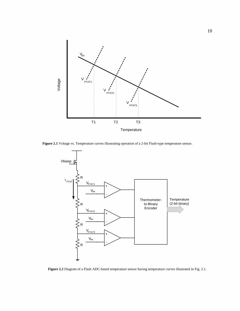
There are a number of different topologies that have been documented in
literature for temperature conversion. One of the simplest and most widely-used performs
conversion using a Flash-type data converter. This type of converter compares a PTAT
voltage to the voltage drop across a forward biased diode-connected PNP transistor
(called hereafter Vbe) using a comparator. Since Vbe has a negative temperature
coefficient (approximately -1.6mV/˚C) and the PTAT voltage has a positive temperature
coefficient, there will be a temperature where the PTAT voltage will be greater than Vbe,
at which point the comparator output will change and indicate the sensor is at the
programmed temperature trip point [3]. Multiple PTAT voltages can be generated using a
current steering DAC (Digital-to-Analog Converter) or a resistor stack with additional
comparators to create multiple programmed temperature trip points. Figures 2.1 and 2.2
illustrate this concept for a simple 2-bit temperature sensor (three temperature trip
points).
10
Temperature
Vo
lta
ge
Vbe
VPTAT1
VPTAT2
VPTAT3
T1 T2 T3
Figure 2.1 Voltage vs. Temperature curves illustrating operation of a 2-bit Flash-type temperature sensor.
Vbiasp
IPTAT
R
R
R
R
+
-
+
-
+
-Vbe
Vbe
Vbe
Temperature
(2-bit binary)
PTAT1
PTAT2
PTAT3
V
V
V
Thermometer-
to-Binary
Encoder
Figure 2.2 Diagram of a Flash ADC-based temperature sensor having temperature curves illustrated in Fig. 2.1.
11
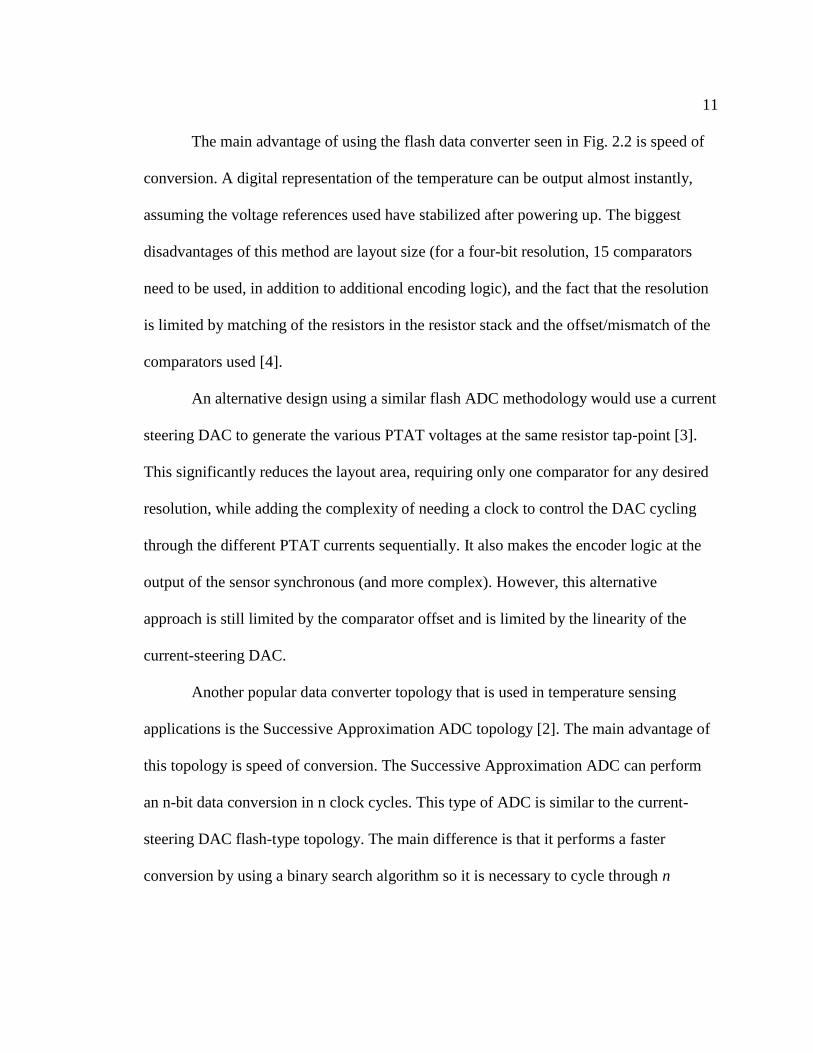
The main advantage of using the flash data converter seen in Fig. 2.2 is speed of
conversion. A digital representation of the temperature can be output almost instantly,
assuming the voltage references used have stabilized after powering up. The biggest
disadvantages of this method are layout size (for a four-bit resolution, 15 comparators
need to be used, in addition to additional encoding logic), and the fact that the resolution
is limited by matching of the resistors in the resistor stack and the offset/mismatch of the
comparators used [4].
An alternative design using a similar flash ADC methodology would use a current
steering DAC to generate the various PTAT voltages at the same resistor tap-point [3].
This significantly reduces the layout area, requiring only one comparator for any desired
resolution, while adding the complexity of needing a clock to control the DAC cycling
through the different PTAT currents sequentially. It also makes the encoder logic at the
output of the sensor synchronous (and more complex). However, this alternative
approach is still limited by the comparator offset and is limited by the linearity of the
current-steering DAC.
Another popular data converter topology that is used in temperature sensing
applications is the Successive Approximation ADC topology [2]. The main advantage of
this topology is speed of conversion. The Successive Approximation ADC can perform
an n-bit data conversion in n clock cycles. This type of ADC is similar to the current-
steering DAC flash-type topology. The main difference is that it performs a faster
conversion by using a binary search algorithm so it is necessary to cycle through n
12
different reference levels instead of 2n different reference levels to perform a complete
digital conversion. This topology is obviously also limited by the offset of the comparator
and the linearity of the DAC.
All of the topologies discussed so far have the main advantage of very fast
temperature-to-digital conversion times, but their resolution is limited by circuit
imperfections such as comparator offset and resistor matching. This means that resistor
trims (and possibly additional trim circuits) are required to obtain desired accuracy,
which requires additional circuit complexity and an additional test step (higher
manufacturing cost). The question should then be asked “Is fast temperature-to-digital
conversion important in a CMOS smart temperature sensor application?”
The maximum rate of temperature change in an integrated temperature sensor
application is determined by a number of factors, including the thermal capacitance of
mass of the object, the heating source and the thermal resistance [2]. For a typical
microprocessor application, the worst case rate would be less than 1 ˚C every 10 ms. This
means that there is plenty of time to make a temperature measurement, so speed of
conversion is not a big concern. For this reason, the focus of this work is on high
resolution temperature conversion, while still keeping power dissipation to a minimum.
2.2 A Novel Approach – Time-to-Digital Conversion
One novel method of doing a temperature-to-digital conversion is presented in
[5]. In this work, a time-to-digital conversion is performed on a pulse whose pulse-width
varies proportionally to absolute temperature (PTAT). This topology seems to be an
13
attractive option for temperature sensing in some applications due to the overall
simplicity of the system. It does not require a system clock, a current or voltage ADC,
complex analog design techniques such as curvature correction and dynamic offset
removal, and can have comparatively small layout area [5]. The authors also
demonstrated very good linearity for their design. The disadvantages of the approach
presented in [5] include reduced noise rejection, large variation in delay due to power
supply variation (since the inverter delay is highly sensitive to power supply variation),
and gain error due to process variation (which can be improved with calibration).
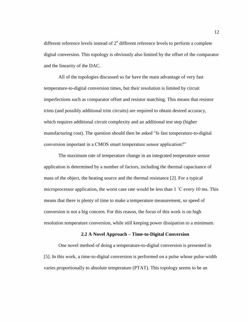
Figure 2.3 shows a diagram of the TDC-based temperature conversion process.
The pulse generator produces the PTAT pulse. That pulse is fed into a time-to-digital
converter (TDC) which then converts the pulse to a digital code proportional to the width
of the input pulse. The resolution of the temperature conversion is then dependent upon
the range of the pulse width over the temperature range of interest and the linear
resolution of the TDC. The TDC also must be thermally insensitive in order to not
introduce distortion into the conversion.
14
Temperature-
to-Pulse
Generator
(PTAT)
SENSE_CMD PTAT Pulse Time-to-
Digital
Converter
0101….
Digital
Output
Figure 2.3 Operation of a Time-to-Digital Converter-based temperature sensor.
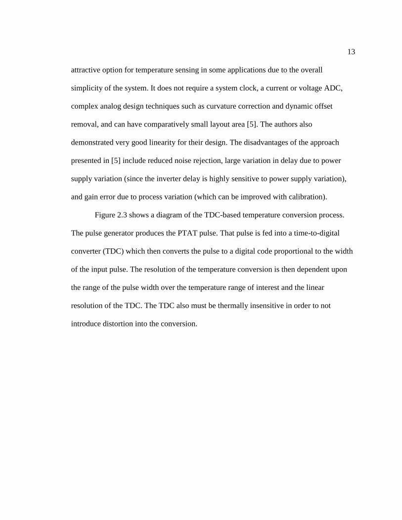
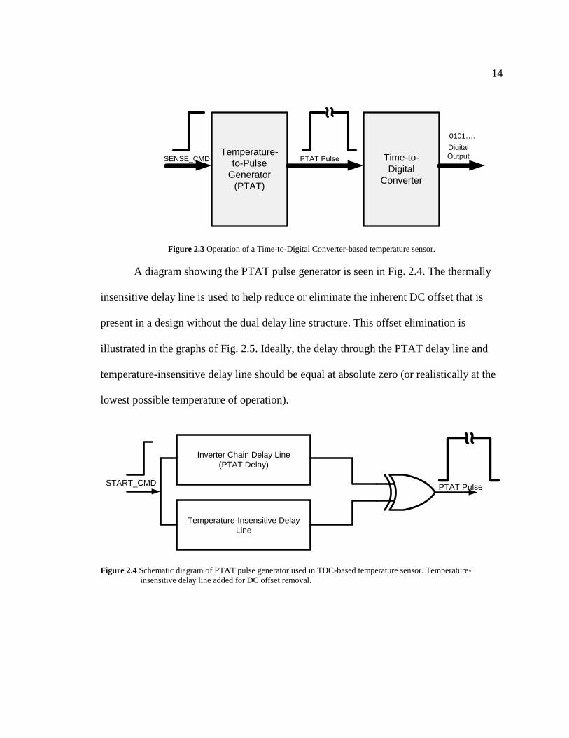
A diagram showing the PTAT pulse generator is seen in Fig. 2.4. The thermally
insensitive delay line is used to help reduce or eliminate the inherent DC offset that is
present in a design without the dual delay line structure. This offset elimination is
illustrated in the graphs of Fig. 2.5. Ideally, the delay through the PTAT delay line and
temperature-insensitive delay line should be equal at absolute zero (or realistically at the
lowest possible temperature of operation).
Inverter Chain Delay Line
(PTAT Delay)
Temperature-Insensitive Delay
Line
START_CMDPTAT Pulse
Figure 2.4 Schematic diagram of PTAT pulse generator used in TDC-based temperature sensor. Temperature-
insensitive delay line added for DC offset removal.
15
Temperature
De
lay
Temperature
De
lay
Temperature-Insensitive Delay
PTAT Delay
PTAT - Temperature-In
sensitive D
elay
Figure 2.5 Graphs illustrating the removal of DC offset from PTAT pulse generator.
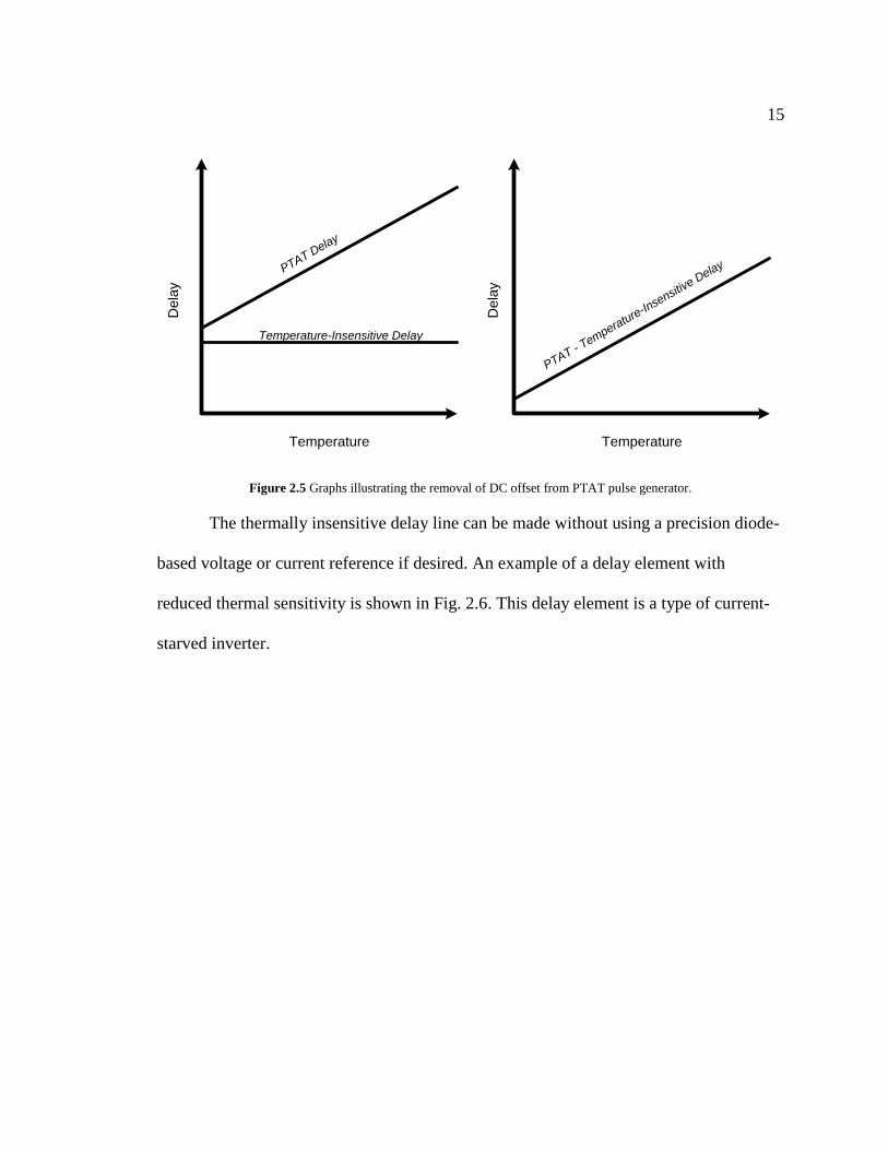
The thermally insensitive delay line can be made without using a precision diode-
based voltage or current reference if desired. An example of a delay element with
reduced thermal sensitivity is shown in Fig. 2.6. This delay element is a type of current-
starved inverter.
16
Figure 2.6 Current-starved inverter-based delay element for use in a TDC-based temperature sensor
The equation for the delay through a voltage controlled delay line (VCDL) made
up of N current-starved inverters is given in [4] as seen in Eq. 2.1, where N is the number
of stages in the VCDL, VDD is the supply voltage, CTOT is the capacitance driven by one
stage of the VCDL, and ID is the biasing current of each stage.
D
TOTD
I
CVDDNt
2 (2.1)
Notice that if the time delay (tD) is differentiated with respect to temperature that
the result is dependent completely on the thermal behavior of ID (assuming CTOT is not
temperature-variant). This means if ID is designed to be more insensitive to temperature,
less distortion will be introduced into the temperature-to-time conversion.
Fig. 2.7 shows the schematic for a cyclic TDC, which is the TDC used in [5].
17
Inverter Chain Delay Line
(PTAT Delay)
Temperature-Insensitive
Delay Line
PTAT Pulse
PTAT Pulse
Temperature-Insensitive
Delay LineCounter
START
Reset
Figure 2.7 Schematic of a TDC-based temperature sensor designed in [5].
Cyclic TDC operation is based on the concept of pulse-shrinking. The logic gates
(OR, AND) provide non-uniform delay elements in the TDC loop, which will shrink the
width of the PTAT input pulse by ΔW, which is dependent on the characteristics of the
logic gates providing different stage delay. The parameter ΔW and the total delay of this
delay line determine the range and resolution of the TDC. One limitation of this type of
TDC is that the PTAT input pulse width must be less than the total delay of the
temperature-insensitive delay line for all operating conditions.
A time-to-digital converter-based temperature sensor was chosen originally
because of its simplicity and small layout size. As was established earlier, the
temperature-sensitivity of a current-starved inverter-based delay line is dependent only on
the temperature behavior of the biasing current. In [5], a delay element with moderately
18
good thermal insensitivity is presented. If a delay element with better (nearly ideal)
thermal insensitivity is used, the overall accuracy of the temperature sense will improve.
Consider the circuit shown in Fig. 2.8 (Note: Vpctat and Vnctat are biasing voltages that
vary complementary to absolute temperature, abbreviated as CTAT).
Figure 2.8 Current-starved inverter with biasing for better temperature insensitivity.
The biasing voltages (Vpptat, Vpctat, Vnptat, and Vnctat) can be generated using
thermal voltage self-biasing techniques using the voltage drop across diode-connected
PNP transitors as a reference [4] (refer back to Fig. 1.3). The disadvantage to this
approach, as opposed to the approach by the authors in [5] is that this type of biasing is
limited by the voltage drop across the diode-connected PNP device (approximately 0.7
V). As CMOS processes and their corresponding supply voltage levels shrink, this
inherent voltage drop can become a serious limiting factor. For this project a Schottky
19
diode, with its inherently lower forward bias voltage drop (approximately 0.3 V), was
used to achieve ultra-low voltage operation. PTAT and CTAT current references that use
Schottky diodes for biasing are show in Fig. 2.9.
VpptatVpctat
Figure 2.9 PTAT (left) and CTAT current references used for biasing voltage-controlled delay lines in a TDC-based
temperature sensor. Schottky diodes are used to improve low-voltage operation of the references.
These currents can then be mirrored to produce Vnptat and Vnctat for biasing the
temperature-insensitive delay line. This design was simulated and proven to work
relatively well under nominal operating conditions. The temperature sensitivity of the
VCDL with the Schottky diode-based biasing circuits was simulated and shown to be
negligible. Figure 2.10 shows simulation results of a 68-stage standard inverter-based
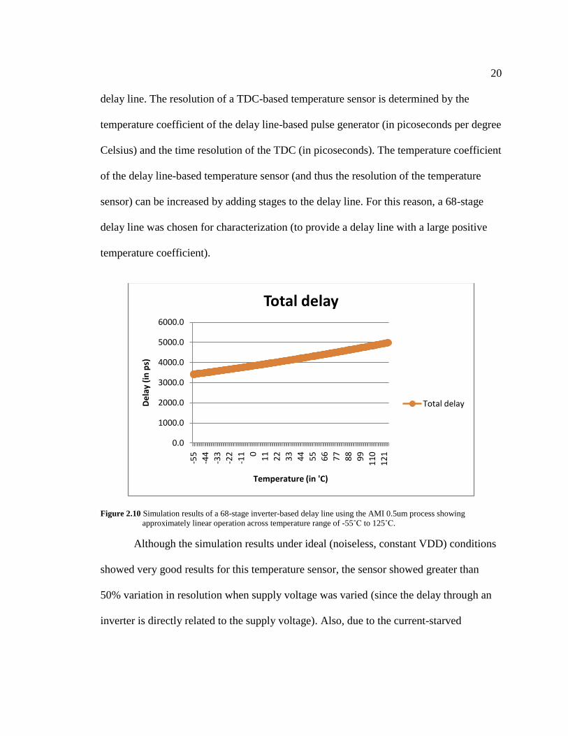
20
delay line. The resolution of a TDC-based temperature sensor is determined by the
temperature coefficient of the delay line-based pulse generator (in picoseconds per degree
Celsius) and the time resolution of the TDC (in picoseconds). The temperature coefficient
of the delay line-based temperature sensor (and thus the resolution of the temperature
sensor) can be increased by adding stages to the delay line. For this reason, a 68-stage
delay line was chosen for characterization (to provide a delay line with a large positive
temperature coefficient).
Figure 2.10 Simulation results of a 68-stage inverter-based delay line using the AMI 0.5um process showing
approximately linear operation across temperature range of -55˚C to 125˚C.
Although the simulation results under ideal (noiseless, constant VDD) conditions
showed very good results for this temperature sensor, the sensor showed greater than
50% variation in resolution when supply voltage was varied (since the delay through an
inverter is directly related to the supply voltage). Also, due to the current-starved
0.0
1000.0
2000.0
3000.0
4000.0
5000.0
6000.0
-55
-44
-33
-22
-11 0
11
22
33
44
55
66
77
88
99
11
0
12
1
De
lay
(in
ps)
Temperature (in 'C)
Total delay
Total delay
21
inverters used in the temperature-insensitive delay line, this sensor is also somewhat
sensitive to circuit noise. The authors in [5] also found this to be the case with their
design. A possible solution to this problem is found in [4] and is presented below.
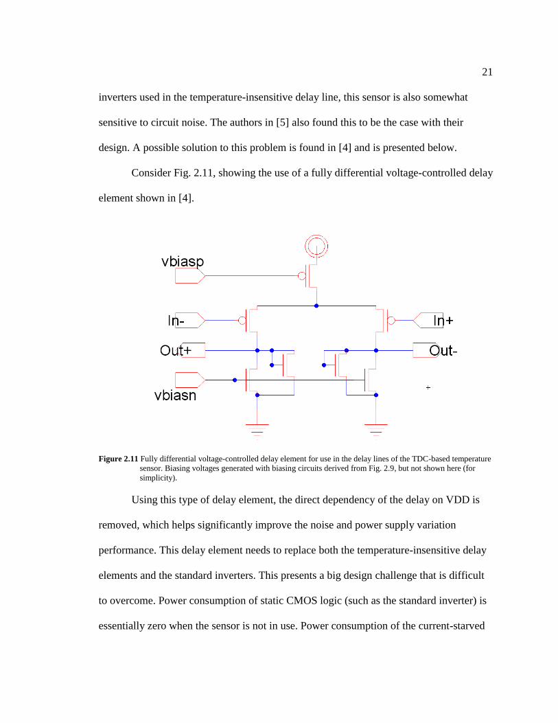
Consider Fig. 2.11, showing the use of a fully differential voltage-controlled delay
element shown in [4].
Figure 2.11 Fully differential voltage-controlled delay element for use in the delay lines of the TDC-based temperature
sensor. Biasing voltages generated with biasing circuits derived from Fig. 2.9, but not shown here (for
simplicity).
Using this type of delay element, the direct dependency of the delay on VDD is
removed, which helps significantly improve the noise and power supply variation
performance. This delay element needs to replace both the temperature-insensitive delay
elements and the standard inverters. This presents a big design challenge that is difficult
to overcome. Power consumption of static CMOS logic (such as the standard inverter) is
essentially zero when the sensor is not in use. Power consumption of the current-starved
22
inverter delay element is also very small, since current only flows through the bias
circuits when the delay line is not in use. With the circuit of Fig. 2.11, current is flowing
through all of the transistors whenever the circuit is powered up. When the delay
elements were designed, satisfactory operation could not be achieved without current
draw of at least 30 µA. Since 50+ delay elements are needed for good temperature range
and resolution for the sensor, this means the circuit will pull more than 1.5 mA whenever
the circuit is powered up, which is generally not acceptable for any mobile or low power
application. For this reason, another topology was used for the final design.
2.3 Sigma-Delta ADC-based Temperature Sensing
Sigma-delta modulators are data converters that trade resolution in time for
resolution in amplitude. This characteristic makes sigma-delta modulation, (sometimes
called delta-sigma modulation or DSM) a very attractive topology for temperature
sensing applications, where the input signal (temperature) changes very slowly, and can
be treated usually as a DC signal for most sensing operations.
Sigma-delta modulation (referred to as DSM hereafter) finds application in many
signal processing circuits, where a high-resolution data conversion is needed. Typically,
lowpass and bandpass modulators are used in communication systems to convert analog
signals into high resolution digital signals to perform signal processing in the digital
domain instead of the analog domain. The use of DSM in signal processing applications
is becoming more prevalent as CMOS process geometries and supply voltages are
23
shrinking, creating significant challenges for accurate signal processing in the analog
domain [6].
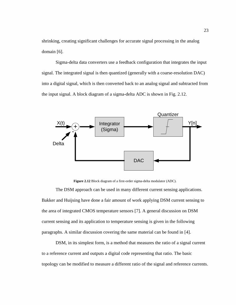
Sigma-delta data converters use a feedback configuration that integrates the input
signal. The integrated signal is then quantized (generally with a coarse-resolution DAC)
into a digital signal, which is then converted back to an analog signal and subtracted from
the input signal. A block diagram of a sigma-delta ADC is shown in Fig. 2.12.
+Integrator
(Sigma)
Quantizer
DAC
Delta
-
X(t) Y[n]
Figure 2.12 Block diagram of a first-order sigma-delta modulator (ADC).
The DSM approach can be used in many different current sensing applications.
Bakker and Huijsing have done a fair amount of work applying DSM current sensing to
the area of integrated CMOS temperature sensors [7]. A general discussion on DSM
current sensing and its application to temperature sensing is given in the following
paragraphs. A similar discussion covering the same material can be found in [4].
DSM, in its simplest form, is a method that measures the ratio of a signal current
to a reference current and outputs a digital code representing that ratio. The basic
topology can be modified to measure a different ratio of the signal and reference currents.
24
This may sometimes be desirable to extend the dynamic range of the converter in a
specific application. A simple circuit demonstrating a basic DSM current sensing
topology is shown in Fig. 2.13.
Vref-
+CLK
Iref
Isignal
Sense_Out
Figure 2.13 Basic DSM current sensing topology sensing the ratio of Isignal to Iref. A ones counter is added to the
output of the clocked comparator, serving as a digital averaging filter.
This circuit contains a signal current source discharging the sense line (positive
input of the clocked comparator). The clocked comparator compares the voltage on the
sense line to a reference voltage and outputs a “1” if it is greater than the reference
voltage, and a “0” otherwise. This output is then inverted and fed back to an NMOS
switch (a PMOS switch if the comparator output is not inverted), which connects a
reference current to the sense line whenever its voltage is less that the reference voltage
(Vref).
One important thing to note regarding the MOS transistor that serves as a switch
to connect and disconnect Iref from the capacitor is that it is not an ideal switch. The
25
PMOS transistor takes a finite amount of time to “turn on” and pass Iref to charge up the
capacitor. If the clock period is short enough such that this “turn on” time is a significant
portion of the clock period (T), the approximate charge added to the capacitor during one
clock period can no longer be approximated accurately as T*Iref. Circuit design
techniques can be used to minimize the effect of the non-ideal switches, but for this
design the clock period is kept large enough such that the T*Iref charge approximation is
accurate.
The reference current Iref serves as a feedback signal. In this topology, the sensor
will not function correctly if Iref is not greater than Isignal under all operating conditions.
Since the average voltage on the sense line (on the capacitor) will be Vref, an equation
can be written to relate the number of ones output from the clocked comparator
(represented by “N”) to the total number of samples (clock cycles, represented by “M”).
This is done by setting the net current charging up the capacitor (when the comparator
output is a “0”) equal to the net current discharging the capacitor (when the comparator
output is a “1”). The equation can be derived in the manner shown below.
IsignalNMIsignalIrefN )()( (2.2)
IsignalMIrefN (2.3)
Iref
Isignal
M
N (2.4)
26
This is a very useful circuit for sensing. Equation 2.4 shows that the resolution of
the sense can be increased simply by increasing the number of samples (M). Since Isignal
is generally a DC current signal (invariant during one sensing operation), the fact that the
current sense will take longer to get higher resolution is not too important for most
applications. Equation 2.5 is derived from Eq. 2.4 to show the minimum resolvable
current that can be sensed with this topology.
M
IrefI ADC min (2.5)
This equation is very useful for determining the number of samples that need to
be performed during a sensing operation for a given reference current. If a resolution of
0.1 µA is needed and the number of samples taken during the sense operation should not
be greater than 512, this equation says that the maximum reference current (feedback
signal) that can be used is 51.2 µA. If a larger reference current is used, a larger number
of samples would be needed to obtain a sensing resolution of 0.1 µA.
The choice for a reference current is also dependent on the range of current that
will be sensed in a given application. For example, current sensed in a Multi-Level Cell
(MLC) resistive memory application may range from 0.1 µA to 10 µA across all values
of resistance being sensed. If resistances can be programmed to obtain 3-bit MLC
operation (eight distinctive levels of resistance), a sensing resolution of 0.05 µA may be
needed. Since Iref must be greater than all possible values for the signal current, Iref
needs to be at least 10.1 µA. A more practical value might be 15 µA. Therefore, in order

27
to obtain the required current resolution, the minimum required number of samples would
be:
30005.0
15
min
uA
uA
I
IrefM
ADC
(2.6)
Another design consideration for this DSM current sensing circuit is the size of
the capacitor used for the sense. Some things to consider when choosing the size of the
capacitor include power consumption (magnitude of Isignal and Iref), layout size of the
capacitor, and clock sampling period (T). In this DSM sensing topology, a range of
voltages should be specified that are allowable on the positive input of the comparator.
This range should be chosen so the voltage on the input does not fall outside the linear
input range of the pre-amplifier clocked comparator’s pre-amplifier. Equation 2.7 shows
how to determine this quantity.
C
TIsignalIref
C
TIsignalMaxV Maxbit ,, (2.7)
Using these equations, the period of the sampling clock (T), size of the sense line
(bitline) capacitor, and magnitude of the currents can be determined for this simple DSM
current sensor. The details of how these quantities are chosen for the integrated
temperature sensing application will be given in chapter 5 of this work.
This sensing topology is a good choice for a high-resolution temperature sensing
application. One of the biggest advantages of this converter is that its resolution can be
improved simply by filtering the output with a digital averaging filter. This topology will

28
be covered in more detail in chapter 5, and the differential topology will also be derived
and examined in depth.
29
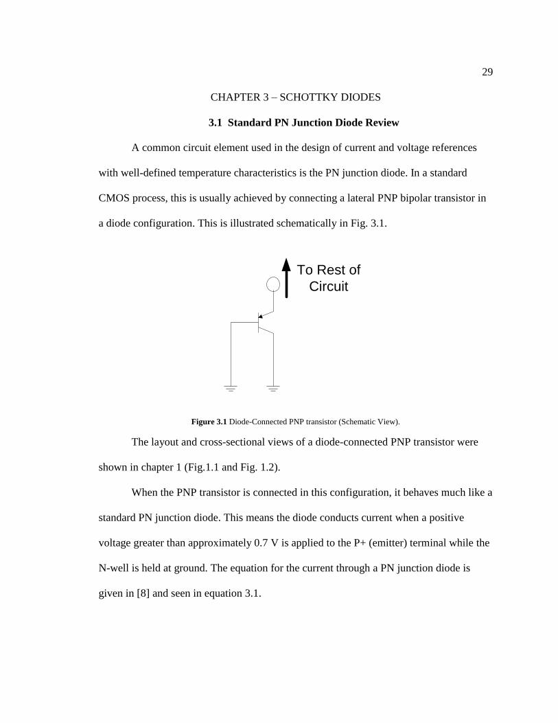
CHAPTER 3 – SCHOTTKY DIODES
3.1 Standard PN Junction Diode Review
A common circuit element used in the design of current and voltage references
with well-defined temperature characteristics is the PN junction diode. In a standard
CMOS process, this is usually achieved by connecting a lateral PNP bipolar transistor in
a diode configuration. This is illustrated schematically in Fig. 3.1.
To Rest of
Circuit
Figure 3.1 Diode-Connected PNP transistor (Schematic View).
The layout and cross-sectional views of a diode-connected PNP transistor were
shown in chapter 1 (Fig.1.1 and Fig. 1.2).
When the PNP transistor is connected in this configuration, it behaves much like a
standard PN junction diode. This means the diode conducts current when a positive
voltage greater than approximately 0.7 V is applied to the P+ (emitter) terminal while the
N-well is held at ground. The equation for the current through a PN junction diode is
given in [8] and seen in equation 3.1.
30
)1('0 nkTqV
eII (3.1)
In this equation k is the Boltzmann Constant (~1.38*10-23
J/K), q is the charge of
an electron (~1.602*10-19
C), n is the emission coefficient (or ideality factor) which
usually lies between 1 and 2. I0’ is called the reverse saturation current, which is the
current flowing through the diode at a strong reverse bias (before breakdown), V is the
potential across the diode junction, and T is the absolute temperature (in Kelvin).
This equation can be used to model the behavior of a PN junction diode with
relative accuracy. A more accurate diode model is used to account for the non-idealities
of the diode in simulation. This model is the Berkeley SPICE semiconductor diode model
[9]. The model was developed at the University of California at Berkeley, for use with
any SPICE simulator. This model accounts for the temperature behavior of the reverse
saturation current (I0’), which is treated simply as a constant in the design equation (3.1).
The Berkeley model also takes into account the bandgap of the diode material, the
junction potential (Vj, a doping dependent parameter), and the series resistance of the
diode (and its dependence on temperature) among other factors. The Berkeley model will
be discussed briefly in the following paragraphs. A more detailed discussion can be found
in [10].
3.2 Semiconductor Diode SPICE Model
The Berkeley Semiconductor Diode SPICE model is a standard model used to
simulate diode performance in integrated circuit design. It uses the equations derived for
current vs. applied voltage for a general device junction. These diode model equations are
31
applicable to any type of semiconductor and/or metal junction, where the materials on
each side of the junction can either be different materials (silicon, germanium, aluminum,
etc.), or the same material with different types of doping (a PN junction).
Equation 3.1 shows the general diode current equation. It is important to note that
I0’ (reverse saturation current) is not a constant term. Instead, the saturation current is
very dependent on temperature and the barrier height or built-in potential at the diode
junction [8]. A band diagram illustrating the built-in (or contact) potential at a PN
junction is shown in Fig. 3.2.
qV0
Evn
Evp
Ecn
Ecp
Eip
EF
EF
Ein
Figure 3.2 Band diagram illustrating a PN junction and how it forms a built-in potential at the junction.
When the P- and N-type semiconductors are brought together, a built-in potential
forms at the junction. This potential (qV0 or qVj) is dependent upon the doping of the two
32
different semiconductor regions (their Fermi levels, EF). In order to forward bias the
diode, a voltage must be applied to the junction to reduce this potential qV0. The junction
potential then changes to q(V0-V), where V is the applied diode voltage [8].
The potential required to forward-bias a PN junction diode is highly dependent on
the bandgap of the semiconductor, and the dopant concentrations at the diode junction.
The bandgap is a parameter that is modeled with the Berkeley model. The equation used
by the model to determine the temperature behavior of the diode saturation current is
shown in Eq. 3.2 [10].
)(
)(exp)(')('
0
0
0
000TTk
TTqE
T
TTITI
g
XTI
(3.2)
In this equation, Eg is the bandgap energy of the semiconductor material, T0 is the
nominal parametric temperature (default value = 27˚C), and XTI is the saturation current
temperature exponent. A list of the parameters that are modeled with the Berkeley model
is shown in Table 3.1 [9].
33
Name Description Units Default
Is saturation current A 1.00E-
14
Rs Ohmic resistance 0
N Emission coefficient - 1
Tt Transit-time Sec 0
Cjo Zero-bias junction cap. F 0
Vj Junction potential V 1
M Grading coefficient - 0.5
Eg Activation energy eV 1.11
Xti Sat.-current temp. exp - 3
Kf Flicker noise coeff. - 0
Af Flicker noise exponent 1 1
Fc Coeff. for forward-bias
depletion capacitance
formula
- 0.5
BV Reverse breakdown
voltage
V Infin.
Ibv Current at breakdown
voltage
A 1.00E-
10
Tnom Parameter measurement
temp.
°C 27
Isr Recombination current
parameter
A 0
Nr Isr emission coeff. - 2
Ikf High-injection knee
current
A Infin.
Tikf Linear Ikf temp coeff. /°C 0
Trs1 linear Rs temp coeff. /°C 0
Trs2 Quadratic Rs temp
coeff.
/°C/°C 0
Table 3.1 Model parameters and their default values for the Berkeley semiconductor diode SPICE model.
34
In a typical CMOS process where diodes can be integrated for use in voltage
references, converters, or temperature sensors, the doping levels are generally limited to
the doping levels required for other devices. Special doping for the diodes in such a
process would add masking levels, making a more complex process which drives up cost
(not desirable). This generally means for a given material (silicon in most cases), the
possible diode forward bias potential is essentially fixed (0.65-0.7 V for silicon, in
general). As operating voltages decrease with more advanced CMOS processes, this
forward bias drop may start to become a limiting factor in a design. If a lower voltage
drop is desired, an alternative device must be found for use in a design.
A Schottky diode is a device that has similar operation to a PN junction diode, but
generally requires a much smaller voltage to achieve forward bias (approximately ½ that
of the PN junction diode). Schottky diode theory will be discussed in detail in the
following section, including a discussion of how the Schottky diode can be modeled with
the Berkeley Semiconductor Diode model.
3.3 Schottky Diode Theory
A Schottky diode is generally formed by a junction of a metal and a lightly-to-
moderately doped semiconductor. Transistor interconnects are generally formed by a
junction of a metal with a heavily-doped semiconductor. Metal-semiconductor junctions
will be discussed in more detail in the following paragraphs.
When a metal with a work function of qΦm comes in contact with a
semiconductor with a work function of qΦs, charge will transfer between the two
35
materials until their Fermi levels align at equilibrium. This is similar to the alignment of
the Fermi levels when a PN semiconductor junction is formed. This forms a potential
barrier at the metal-semiconductor junction called a Schottky barrier [8]. A band diagram
illustrating the formation of the Schottky barrier is shown in Fig. 3.3.
Metal
qΦB
qΦm-ᵡ=
EFm
EFs
Figure 3.3 Band diagram of a metal-semiconductor junction showing the formation of a Schottky barrier at the
junction.
The Schottky barrier height (qΦB) is shown to be dependent on the work function
of the metal and a quantity known as the electron affinity (X). This barrier is similar to
the barrier formed at a PN junction, except the barrier height of a Schottky junction is
generally significantly lower than the barrier at a PN junction (resulting in a forward bias
approximately ½ that of a PN junction diode). The equation for saturation current (3.2)
can be substituted into the diode current equation (3.1) to show how the diode current is
very dependent upon this barrier height.
36
)1(expexp)('
2
0
00
nkT
qV
kT
q
T
TTII DB
D (3.3)
This equation shows that the saturation current increases as the Schottky barrier
height is decreased. The value n is similar to that for a PN junction diode, being a number
that lies between 1 and 2 [10]. Another important thing to notice is that XTI (the
saturation current temperature exponent) is generally 2 for Schottky diodes. PN junction
diodes generally have XTI=3. Remembering these parameters, and the origin of the
increase reverse saturation current for Schottky diodes will be very important in
producing an accurate model of the diode. This will be discussed in more detail in
chapters 4-6.
The Schottky barrier height can vary significantly in a given process due to a
couple of factors. The barrier height is very much dependent upon the doping of the
semiconductor at the diode junction. For most CMOS processes, this is not closely
monitored [4]. Also, the barrier height can vary significantly due to interface states and
image charges that can exist at the junction. To reduce variation in these characteristics, a
very clean metal-semiconductor interface is desirable [8]. In order to help with this, a
very thin interfacial layer can be grown at the junction to make a very clean interface.
Figs. 3.4 and 3.5 show layout and cross-sectional views of a typical Schottky
diode laid out in a CMOS process.
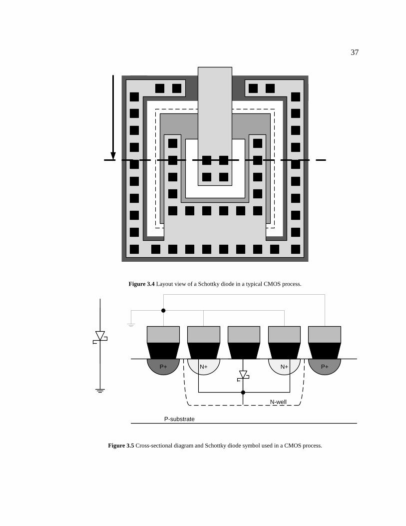
37
C
C
C
C
C
CC
CC
Figure 3.4 Layout view of a Schottky diode in a typical CMOS process.
P-substrate
N-well
P+ P+N+ N+
Figure 3.5 Cross-sectional diagram and Schottky diode symbol used in a CMOS process.
38
Notice the Schottky diode differs from the diode-connected PNP device by the
anode connecting directly to the n-well instead of to an n+-doped region. A Schottky
diode can also be formed with a metal connection to a p-well (without a p+ implant
region), but this requires a triple well process (one that can create separate, electrically
isolated p-well regions). Since the process used for this design is not a triple-well process,
this will not be discussed further.
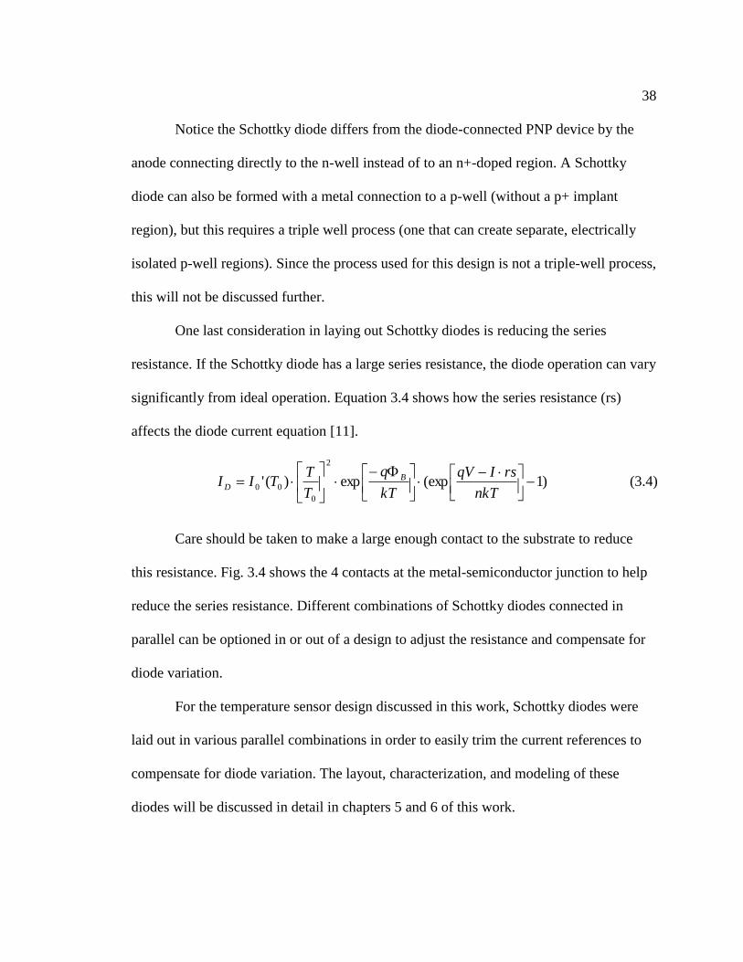
One last consideration in laying out Schottky diodes is reducing the series
resistance. If the Schottky diode has a large series resistance, the diode operation can vary
significantly from ideal operation. Equation 3.4 shows how the series resistance (rs)
affects the diode current equation [11].
)1(expexp)('
2
0
00
nkT
rsIqV
kT
q
T
TTII B
D (3.4)
Care should be taken to make a large enough contact to the substrate to reduce
this resistance. Fig. 3.4 shows the 4 contacts at the metal-semiconductor junction to help
reduce the series resistance. Different combinations of Schottky diodes connected in
parallel can be optioned in or out of a design to adjust the resistance and compensate for
diode variation.
For the temperature sensor design discussed in this work, Schottky diodes were
laid out in various parallel combinations in order to easily trim the current references to
compensate for diode variation. The layout, characterization, and modeling of these
diodes will be discussed in detail in chapters 5 and 6 of this work.
39
CHAPTER 4 – CURRENT REFERENCES AND CURRENT MIRRORING
4.1 Introduction
In analog circuit design, precision current and voltage reference circuits are
required often for circuit biasing. Many applications require references that have minimal
variation across process, temperature, and power supply levels. For applications such as
temperature sensing, voltage and current references are needed that have very well-
defined temperature characteristics in order to measure temperature accurately. The
design of current references with well-defined temperature characteristics will be covered
in this chapter.
The PN junction diode is commonly used together with resistors and MOSFETs
to generate current references that vary either proportionally to absolute temperature
(PTAT), complementary to absolute temperature (CTAT), or are insensitive to variations
in temperature. As discussed in chapter 1, supply voltages continue to decrease as process
dimensions shrink. As this happens, the inherent voltage drop across a PN junction diode
(approximately 0.7 V) will start to become a limiting factor in the design of these
references. For this reason, reference design using a metal-semiconductor junction
(Schottky) diode is also discussed in detail in this chapter.
This chapter will also cover current mirroring. Mirrored currents will vary with
temperature in the same way that its reference current varies. In a fully differential
current sensing application, it is extremely important to accurately match mirrored
currents, which makes this an important topic of discussion.

40
4.2 Review of CMOS Current Reference Design
As an introduction to this topic, consider a common, robust current reference
design that is commonly used in CMOS processes without using a parasitic diode
structure. This reference is commonly referred to as the Beta Multiplier Reference
(BMR). A BMR schematic in a short-channel CMOS process is shown in Fig. 4.1 [4].
For simplicity, the startup circuit is not shown.
Figure 4.1 Beta Multiplier Reference Circuit used in a short-channel CMOS process.
In this circuit, the NMOS transistor widths are sized such that M2 is K times
wider than M1. A resistor is connected to the source M2 to set the current in the
reference. A differential amplifier is connected to the transistor drains to force the same
41
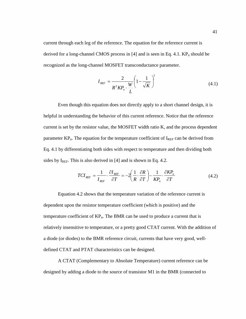
current through each leg of the reference. The equation for the reference current is
derived for a long-channel CMOS process in [4] and is seen in Eq. 4.1. KPn should be
recognized as the long-channel MOSFET transconductance parameter.
2
2
11
2
K
L
WKPR
I
n
REF (4.1)
Even though this equation does not directly apply to a short channel design, it is
helpful in understanding the behavior of this current reference. Notice that the reference
current is set by the resistor value, the MOSFET width ratio K, and the process dependent
parameter KPn. The equation for the temperature coefficient of IREF can be derived from
Eq. 4.1 by differentiating both sides with respect to temperature and then dividing both
sides by IREF. This is also derived in [4] and is shown in Eq. 4.2.
T
KP
KPT
R
RT
I
ITCI n
n
REF
REF
REF
112
1 (4.2)
Equation 4.2 shows that the temperature variation of the reference current is
dependent upon the resistor temperature coefficient (which is positive) and the
temperature coefficient of KPn. The BMR can be used to produce a current that is
relatively insensitive to temperature, or a pretty good CTAT current. With the addition of
a diode (or diodes) to the BMR reference circuit, currents that have very good, well-
defined CTAT and PTAT characteristics can be designed.
A CTAT (Complementary to Absolute Temperature) current reference can be
designed by adding a diode to the source of transistor M1 in the BMR (connected to
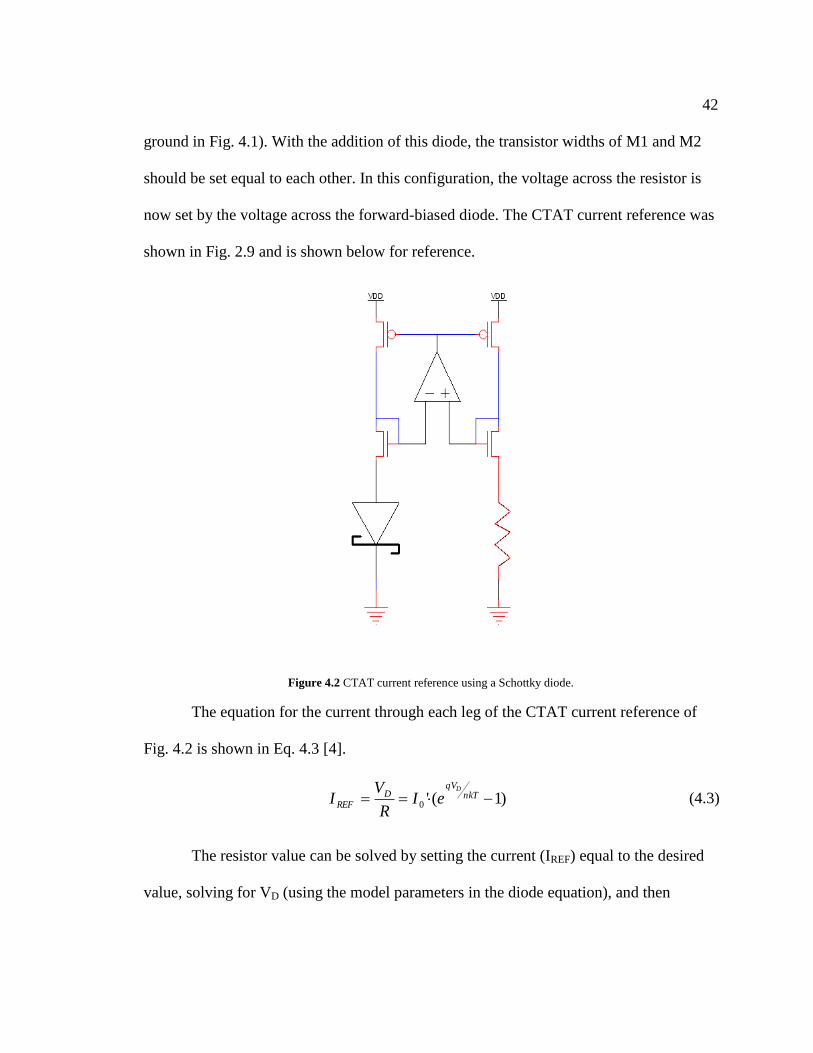
42
ground in Fig. 4.1). With the addition of this diode, the transistor widths of M1 and M2
should be set equal to each other. In this configuration, the voltage across the resistor is
now set by the voltage across the forward-biased diode. The CTAT current reference was
shown in Fig. 2.9 and is shown below for reference.
Figure 4.2 CTAT current reference using a Schottky diode.
The equation for the current through each leg of the CTAT current reference of
Fig. 4.2 is shown in Eq. 4.3 [4].
)1('0 nkTqV
DREF
D
eIR
VI (4.3)
The resistor value can be solved by setting the current (IREF) equal to the desired
value, solving for VD (using the model parameters in the diode equation), and then
43
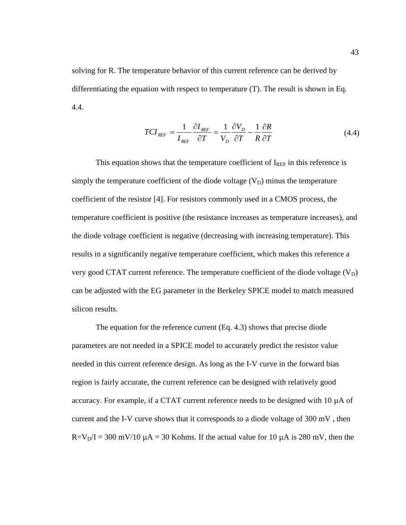
solving for R. The temperature behavior of this current reference can be derived by
differentiating the equation with respect to temperature (T). The result is shown in Eq.
4.4.
T
R
RT
V
VT
I
ITCI D
D
REF
REF
REF
111 (4.4)
This equation shows that the temperature coefficient of IREF in this reference is
simply the temperature coefficient of the diode voltage (VD) minus the temperature
coefficient of the resistor [4]. For resistors commonly used in a CMOS process, the
temperature coefficient is positive (the resistance increases as temperature increases), and
the diode voltage coefficient is negative (decreasing with increasing temperature). This
results in a significantly negative temperature coefficient, which makes this reference a
very good CTAT current reference. The temperature coefficient of the diode voltage (VD)
can be adjusted with the EG parameter in the Berkeley SPICE model to match measured
silicon results.
The equation for the reference current (Eq. 4.3) shows that precise diode
parameters are not needed in a SPICE model to accurately predict the resistor value
needed in this current reference design. As long as the I-V curve in the forward bias
region is fairly accurate, the current reference can be designed with relatively good
accuracy. For example, if a CTAT current reference needs to be designed with 10 µA of
current and the I-V curve shows that it corresponds to a diode voltage of 300 mV , then
R=VD/I = 300 mV/10 µA = 30 Kohms. If the actual value for 10 µA is 280 mV, then the
44
reference current will be within 10% of the desired value. This does not mean that having
accurate diode parameters (n, XTI, I0’, etc.) is not important for an accurate design. When
designing a PTAT current source, the importance of an accurate model will become more
obvious.
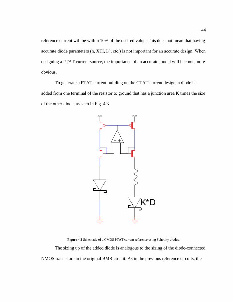
To generate a PTAT current building on the CTAT current design, a diode is
added from one terminal of the resistor to ground that has a junction area K times the size
of the other diode, as seen in Fig. 4.3.
Figure 4.3 Schematic of a CMOS PTAT current reference using Schottky diodes.
The sizing up of the added diode is analogous to the sizing of the diode-connected
NMOS transistors in the original BMR circuit. As in the previous reference circuits, the
45
differential amplifier is added to force the same current (IPTAT) through both legs of the
reference circuit. The equation for the PTAT current is derived in [4] and is shown in Eq.
4.5.
TqR
KnkI PTAT
ln (4.5)
By inspection, it can be seen that the current increases proportionally to
temperature. If the temperature coefficient of the resistor R is zero, this circuit produces a
current that increases linearly with temperature, having a slope of nk*ln(K)/(qR). Since
the resistor increases with temperature (has a positive temperature coefficient), the
temperature coefficient will not be a constant number. As was done in the CTAT current
example, the temperature coefficient for the PTAT current can be derived by
differentiating IPTAT with respect to temperature and dividing by IPTAT. This is seen in Eq.
4.6.
T
R
RTT
I
ITCI PTAT
PTAT
PTAT
111 (4.6)
The temperature coefficient for IPTAT is not a constant number as it was in the case
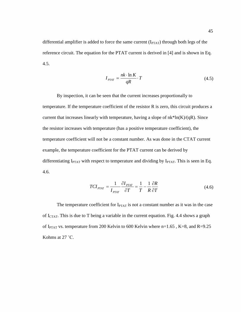
of ICTAT. This is due to T being a variable in the current equation. Fig. 4.4 shows a graph
of IPTAT vs. temperature from 200 Kelvin to 600 Kelvin where n=1.65 , K=8, and R=9.25
Kohms at 27 ˚C.
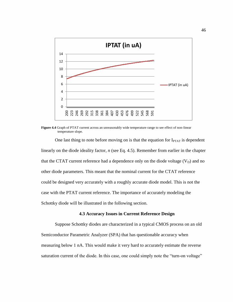
46
Figure 4.4 Graph of PTAT current across an unreasonably wide temperature range to see effect of non-linear
temperature slope.
One last thing to note before moving on is that the equation for IPTAT is dependent
linearly on the diode ideality factor, n (see Eq. 4.5). Remember from earlier in the chapter
that the CTAT current reference had a dependence only on the diode voltage (VD) and no
other diode parameters. This meant that the nominal current for the CTAT reference
could be designed very accurately with a roughly accurate diode model. This is not the
case with the PTAT current reference. The importance of accurately modeling the
Schottky diode will be illustrated in the following section.
4.3 Accuracy Issues in Current Reference Design
Suppose Schottky diodes are characterized in a typical CMOS process on an old
Semiconductor Parametric Analyzer (SPA) that has questionable accuracy when
measuring below 1 nA. This would make it very hard to accurately estimate the reverse
saturation current of the diode. In this case, one could simply note the “turn-on voltage”
0
2
4
6
8
10
12
14
20
0
22
3
24
6
26
9
29
2
31
5
33
8
36
1
38
4
40
7
43
0
45
3
47
6
49
9
52
2
54
5
56
8
59
1
IPTAT (in uA)
IPTAT (in uA)
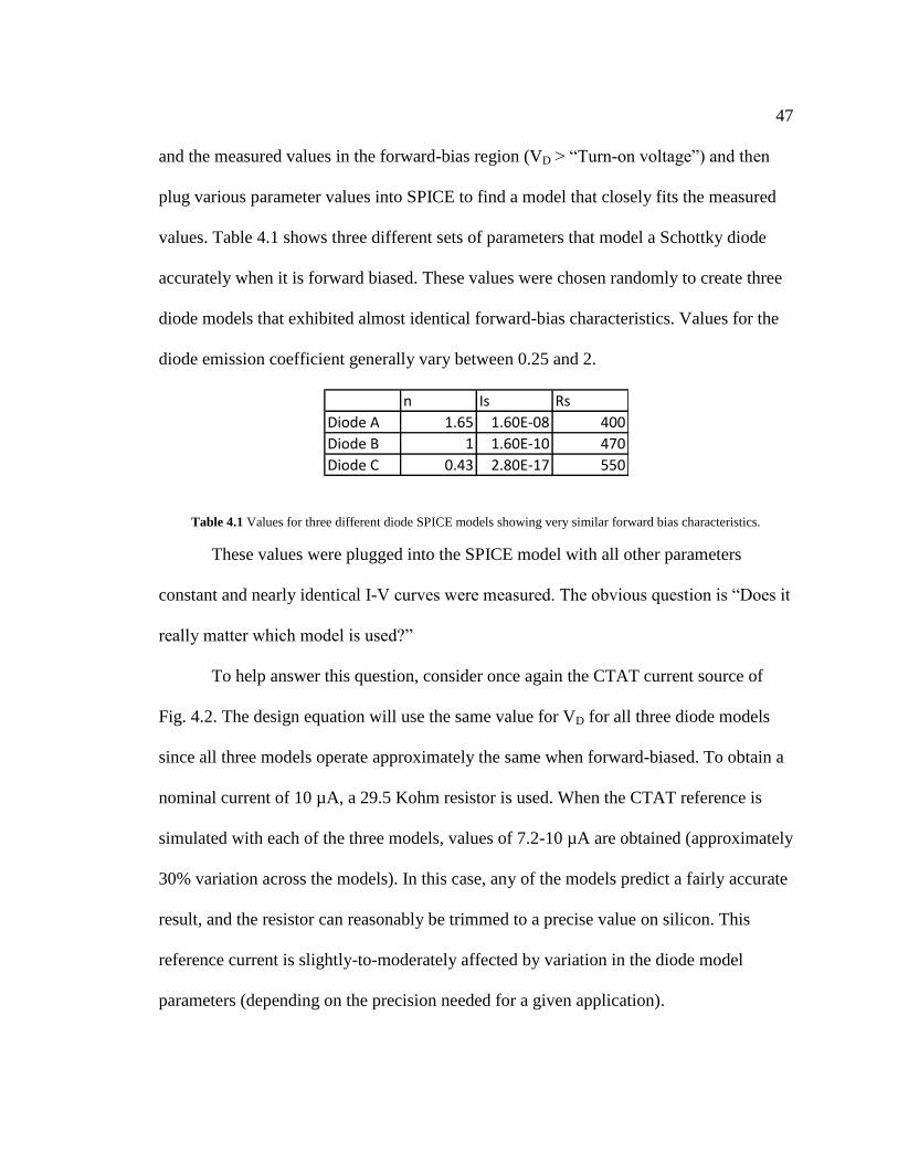
47
and the measured values in the forward-bias region (VD > “Turn-on voltage”) and then
plug various parameter values into SPICE to find a model that closely fits the measured
values. Table 4.1 shows three different sets of parameters that model a Schottky diode
accurately when it is forward biased. These values were chosen randomly to create three
diode models that exhibited almost identical forward-bias characteristics. Values for the
diode emission coefficient generally vary between 0.25 and 2.
Table 4.1 Values for three different diode SPICE models showing very similar forward bias characteristics.
These values were plugged into the SPICE model with all other parameters
constant and nearly identical I-V curves were measured. The obvious question is “Does it
really matter which model is used?”
To help answer this question, consider once again the CTAT current source of
Fig. 4.2. The design equation will use the same value for VD for all three diode models
since all three models operate approximately the same when forward-biased. To obtain a
nominal current of 10 µA, a 29.5 Kohm resistor is used. When the CTAT reference is
simulated with each of the three models, values of 7.2-10 µA are obtained (approximately
30% variation across the models). In this case, any of the models predict a fairly accurate
result, and the resistor can reasonably be trimmed to a precise value on silicon. This
reference current is slightly-to-moderately affected by variation in the diode model
parameters (depending on the precision needed for a given application).
n Is Rs
Diode A 1.65 1.60E-08 400
Diode B 1 1.60E-10 470
Diode C 0.43 2.80E-17 550
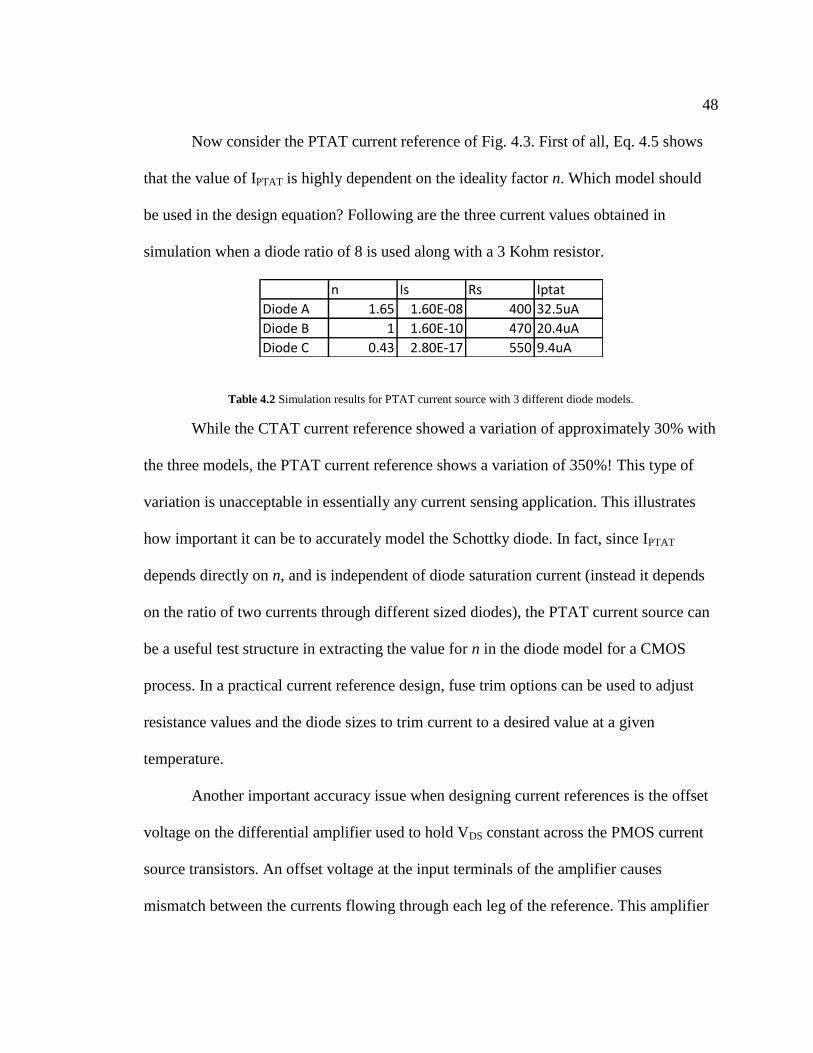
48
Now consider the PTAT current reference of Fig. 4.3. First of all, Eq. 4.5 shows
that the value of IPTAT is highly dependent on the ideality factor n. Which model should
be used in the design equation? Following are the three current values obtained in
simulation when a diode ratio of 8 is used along with a 3 Kohm resistor.
Table 4.2 Simulation results for PTAT current source with 3 different diode models.
While the CTAT current reference showed a variation of approximately 30% with
the three models, the PTAT current reference shows a variation of 350%! This type of
variation is unacceptable in essentially any current sensing application. This illustrates
how important it can be to accurately model the Schottky diode. In fact, since IPTAT
depends directly on n, and is independent of diode saturation current (instead it depends
on the ratio of two currents through different sized diodes), the PTAT current source can
be a useful test structure in extracting the value for n in the diode model for a CMOS
process. In a practical current reference design, fuse trim options can be used to adjust
resistance values and the diode sizes to trim current to a desired value at a given
temperature.
Another important accuracy issue when designing current references is the offset
voltage on the differential amplifier used to hold VDS constant across the PMOS current
source transistors. An offset voltage at the input terminals of the amplifier causes
mismatch between the currents flowing through each leg of the reference. This amplifier
n Is Rs Iptat
Diode A 1.65 1.60E-08 400 32.5uA
Diode B 1 1.60E-10 470 20.4uA
Diode C 0.43 2.80E-17 550 9.4uA
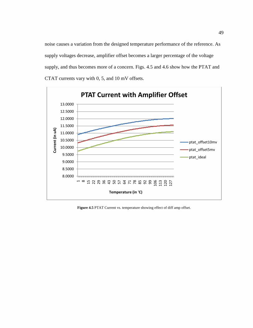
49
noise causes a variation from the designed temperature performance of the reference. As
supply voltages decrease, amplifier offset becomes a larger percentage of the voltage
supply, and thus becomes more of a concern. Figs. 4.5 and 4.6 show how the PTAT and
CTAT currents vary with 0, 5, and 10 mV offsets.
Figure 4.5 PTAT Current vs. temperature showing effect of diff amp offset.
8.0000
8.5000
9.0000
9.5000
10.0000
10.5000
11.0000
11.5000
12.0000
12.5000
13.0000
1 81
52
22
93
64
35
05
76
47
17
88
59
29
91
06
11
31
20
12
7
Cu
rre
nt
(in
uA
)
Temperature (in 'C)
PTAT Current with Amplifier Offset
ptat_offset10mv
ptat_offset5mv
ptat_ideal
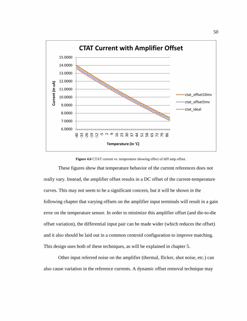
50
Figure 4.6 CTAT current vs. temperature showing effect of diff amp offset.
These figures show that temperature behavior of the current references does not
really vary. Instead, the amplifier offset results in a DC offset of the current-temperature
curves. This may not seem to be a significant concern, but it will be shown in the
following chapter that varying offsets on the amplifier input terminals will result in a gain
error on the temperature sensor. In order to minimize this amplifier offset (and die-to-die
offset variation), the differential input pair can be made wider (which reduces the offset)
and it also should be laid out in a common centroid configuration to improve matching.
This design uses both of these techniques, as will be explained in chapter 5.
Other input referred noise on the amplifier (thermal, flicker, shot noise, etc.) can
also cause variation in the reference currents. A dynamic offset removal technique may
6.0000
7.0000
8.0000
9.0000
10.0000
11.0000
12.0000
13.0000
14.0000
15.0000
-40
-33
-26
-19
-12 -5 2 9
16
23
30
37
44
51
58
65
72
79
86
Cu
rre
nt
(in
uA
)
Temperature (in 'C)
CTAT Current with Amplifier Offset
ctat_offset10mv
ctat_offset5mv
ctat_ideal
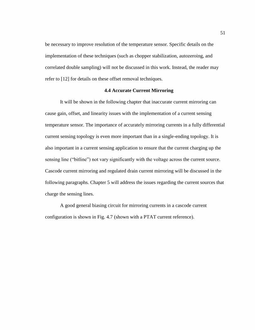
51
be necessary to improve resolution of the temperature sensor. Specific details on the
implementation of these techniques (such as chopper stabilization, autozeroing, and
correlated double sampling) will not be discussed in this work. Instead, the reader may
refer to [12] for details on these offset removal techniques.
4.4 Accurate Current Mirroring
It will be shown in the following chapter that inaccurate current mirroring can
cause gain, offset, and linearity issues with the implementation of a current sensing
temperature sensor. The importance of accurately mirroring currents in a fully differential
current sensing topology is even more important than in a single-ending topology. It is
also important in a current sensing application to ensure that the current charging up the
sensing line (“bitline”) not vary significantly with the voltage across the current source.
Cascode current mirroring and regulated drain current mirroring will be discussed in the
following paragraphs. Chapter 5 will address the issues regarding the current sources that
charge the sensing lines.
A good general biasing circuit for mirroring currents in a cascode current
configuration is shown in Fig. 4.7 (shown with a PTAT current reference).
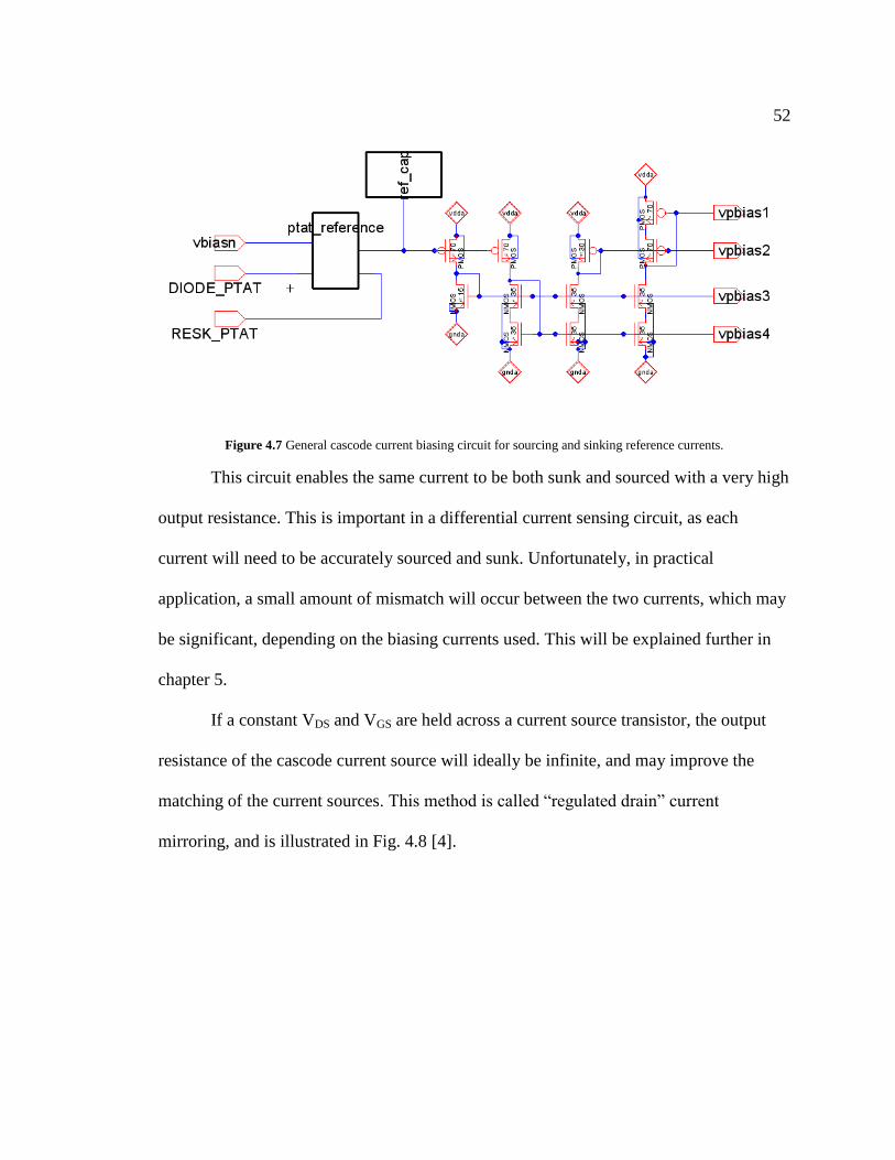
52
Figure 4.7 General cascode current biasing circuit for sourcing and sinking reference currents.
This circuit enables the same current to be both sunk and sourced with a very high
output resistance. This is important in a differential current sensing circuit, as each
current will need to be accurately sourced and sunk. Unfortunately, in practical
application, a small amount of mismatch will occur between the two currents, which may
be significant, depending on the biasing currents used. This will be explained further in
chapter 5.
If a constant VDS and VGS are held across a current source transistor, the output
resistance of the cascode current source will ideally be infinite, and may improve the
matching of the current sources. This method is called “regulated drain” current
mirroring, and is illustrated in Fig. 4.8 [4].
53
Figure 4.8 Regulated drain NMOS current mirror.
In summary, it is important in a current sensing application to accurately match all
of the currents being mirrored in the circuit. Any mismatch in mirrored currents will
directly contribute to gain error and nonlinearity in the temperature sensor. The impact of
these inaccuracies will depend on the application. It is also important to mirror currents
so the sources/sinks will have a very high output resistance, as this will also improve the
accuracy of the current sense. Chapter 5 will discuss the integration of the current sources
designed in this chapter into a fully differential DSM temperature sensor. Further
discussion regarding low voltage performance and impact on the accuracy of the current
sense will also be done in chapter 5.
54
CHAPTER 5 – FULLY DIFFERENTIAL SIGMA-DELTA TEMPERATURE SENSOR
5.1 Introduction
The original objective for this project was to design, manufacture, and test a high
resolution temperature sensor suitable for integration into any an ASIC designed in a
CMOS process. The sensor needed to be designed for use in an advanced CMOS process
(with a supply voltage approaching 1 V) and have sufficient resolution for on-chip
process regulation and continuous temperature readout for system process control. The
previous four chapters have discussed design of the individual components of the sensor.
The following sections will detail the usage of these components to implement a high
resolution temperature sensor for operation at very low voltages.
5.2 Temperature Sensitive Current References
Current references whose currents vary proportional to absolute temperature
(PTAT) and complementary to absolute temperature (CTAT) serve as input to the current
sensing DSM temperature sensor. The design process for these current references was
covered in detail in chapter 4. When the traditional diode-connected PNP bipolar
transistor is replace with a Schottky diode, the operating range of the current references
will be lowered by approximately 300-350 mV. This is due to the lower forward-bias
voltage (due to a much lower potential barrier at the junction) as discussed in chapter 3.
PTAT and CTAT current references were designed to produce 10 µA currents
using PN junction diodes and also using Schottky diodes. These references were then
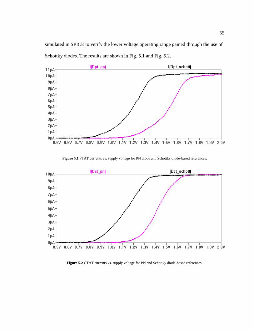
55
simulated in SPICE to verify the lower voltage operating range gained through the use of
Schottky diodes. The results are shown in Fig. 5.1 and Fig. 5.2.
Figure 5.1 PTAT currents vs. supply voltage for PN diode and Schottky diode-based references.
Figure 5.2 CTAT currents vs. supply voltage for PN and Schottky diode-based references.

56
Notice that both Schottky diode-based references (Dct_schott, and Dpt_schott)
start conducting the desired reference currents with supply voltages at least 300 mV
lower than the references designed with PN junction diode-based references. This helps
to achieve the objective of lower voltage operation for the sensor. It is important to note
that this sensor was design using a 5 V, 0.5 µm analog process where the threshold
voltages range from 700 to 950 mV. If these current references were implemented in a
process with lower nominal supply voltages (and thus lower MOSFET threshold
voltages), the 300 mV increase in low voltage margin would be even more significant.
One unfortunate characteristic of a submicron CMOS process is the variation in
implant doping levels (both across wafer and across process runs) that cause variation in
sheet resistance for integrated resistors and also the barrier height of Schottky diodes. For
this reason, it is necessary to design trim options (through fuses or programmable
registers) to trim the references reasonably close to their desired value. This trimming
helps to improve variation of the temperature slope from die to die. The temperature
sensor described in this paper was designed to enable off-chip programming of the
resistors and diodes used in these references.
In order to accurately simulate these references, it is important to have an accurate
model of the diode for the design phase. For the AMI C5N process used to manufacture
this sensor, Schottky diodes had already been characterized thoroughly in the design of a
Schottky diode-based bandgap voltage reference [13]. The design parameters derived in
this paper were used to model the Schottky diodes during the design phase of this project.
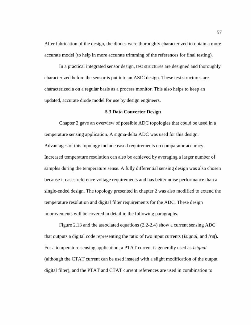
57
After fabrication of the design, the diodes were thoroughly characterized to obtain a more
accurate model (to help in more accurate trimming of the references for final testing).
In a practical integrated sensor design, test structures are designed and thoroughly
characterized before the sensor is put into an ASIC design. These test structures are
characterized a on a regular basis as a process monitor. This also helps to keep an
updated, accurate diode model for use by design engineers.
5.3 Data Converter Design
Chapter 2 gave an overview of possible ADC topologies that could be used in a
temperature sensing application. A sigma-delta ADC was used for this design.
Advantages of this topology include eased requirements on comparator accuracy.
Increased temperature resolution can also be achieved by averaging a larger number of
samples during the temperature sense. A fully differential sensing design was also chosen
because it eases reference voltage requirements and has better noise performance than a
single-ended design. The topology presented in chapter 2 was also modified to extend the
temperature resolution and digital filter requirements for the ADC. These design
improvements will be covered in detail in the following paragraphs.
Figure 2.13 and the associated equations (2.2-2.4) show a current sensing ADC
that outputs a digital code representing the ratio of two input currents (Isignal, and Iref).
For a temperature sensing application, a PTAT current is generally used as Isignal
(although the CTAT current can be used instead with a slight modification of the output
digital filter), and the PTAT and CTAT current references are used in combination to
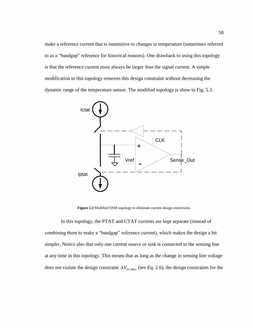
58
make a reference current that is insensitive to changes in temperature (sometimes referred
to as a “bandgap” reference for historical reasons). One drawback to using this topology
is that the reference current must always be larger than the signal current. A simple
modification to this topology removes this design constraint without decreasing the
dynamic range of the temperature sensor. The modified topology is show in Fig. 5.3.
Vref-
+CLK
Ictat
Iptat
Sense_Out
Figure 5.3 Modified DSM topology to eliminate current design restrictions.
In this topology, the PTAT and CTAT currents are kept separate (instead of
combining them to make a “bandgap” reference current), which makes the design a bit
simpler. Notice also that only one current source or sink is connected to the sensing line
at any time in this topology. This means that as long as the change in sensing line voltage
does not violate the design constraint MaxbitV , (see Eq. 2.6), the design constraints for the
59
magnitudes of the signal currents are eliminated. Equations 5.1-5.3 show the derivation
of the equations governing the operation of the circuit.
PTATCTAT INMIN )()( (5.1)
PTATCTATPTAT IMIIN )( (5.2)
CTATPTAT
PTAT
II
I
M
N
(5.3)
Since the reference current in the original topology is simply the sum of PTAT
and CTAT currents, this equation for the output of this modified DSM topology is
identical to that of the original temperature sensor.
One important thing to note in the Eq. 5.3 is that the output code is not directly
affected by the size of the sampling capacitor. The sensing capacitor should be chosen to
satisfy the design constraint for ΔVbit,max (see Eq. 2.7). The period of the sampling clock
should also be a consideration in choosing the size of the capacitor. If the capacitor value
is too small, it will be very susceptible to process variation. If the capacitor is too large, it
will adversely affect the sensor noise performance (since ΔVbit,max will be small compared
to the magnitude of a noise voltage that may couple to the sensing line). For this design,
an 8 pF capacitor was used because it satisfied the design constraints and exhibited good
noise performance at the desired frequency of the sampling clock (10-50 MHz).
To illustrate the performance of a temperature sensor using this configuration,
suppose that a PTAT current source is designed to vary from 9 µA at -40 ˚C to 14 µA at
90 ˚C. A CTAT current is designed to have a matching temperature coefficient (so the
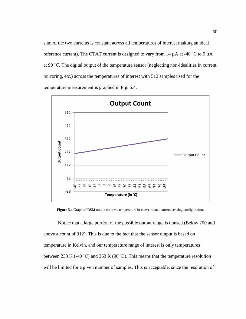
60
sum of the two currents is constant across all temperatures of interest making an ideal
reference current). The CTAT current is designed to vary from 14 µA at -40 ˚C to 9 µA
at 90 ˚C. The digital output of the temperature sensor (neglecting non-idealities in current
mirroring, etc.) across the temperatures of interest with 512 samples used for the
temperature measurement is graphed in Fig. 5.4.
Figure 5.4 Graph of DSM output code vs. temperature in conventional current sensing configuration.
Notice that a large portion of the possible output range is unused (Below 200 and
above a count of 312). This is due to the fact that the sensor output is based on
temperature in Kelvin, and our temperature range of interest is only temperatures
between 233 K (-40 ˚C) and 363 K (90 ˚C). This means that the temperature resolution
will be limited for a given number of samples. This is acceptable, since the resolution of
-88
12
112
212
312
412
512
-40
-33
-26
-19
-12 -5 2 9
16
23
30
37
44
51
58
65
72
79
86
Ou
tpu
t C
ou
nt
Temperature (in 'C)
Output Count
Output Count
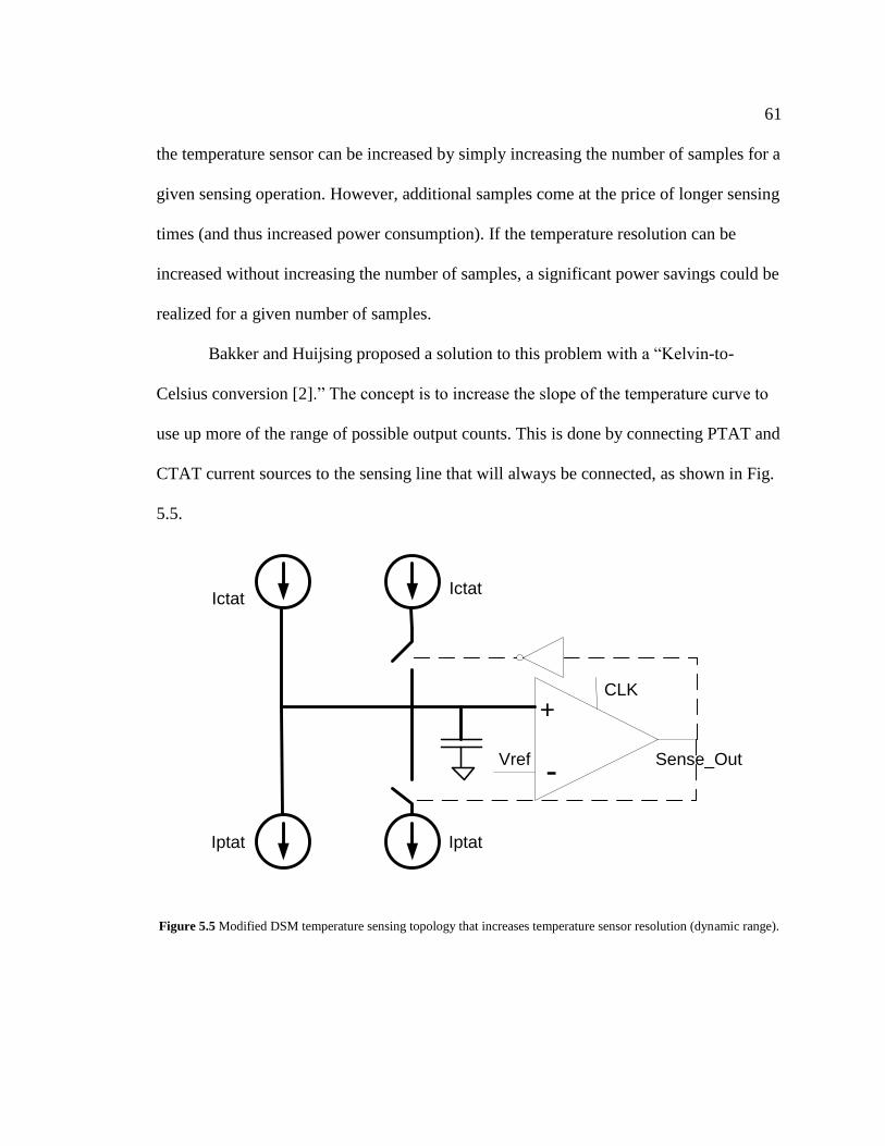
61
the temperature sensor can be increased by simply increasing the number of samples for a
given sensing operation. However, additional samples come at the price of longer sensing
times (and thus increased power consumption). If the temperature resolution can be
increased without increasing the number of samples, a significant power savings could be
realized for a given number of samples.
Bakker and Huijsing proposed a solution to this problem with a “Kelvin-to-
Celsius conversion [2].” The concept is to increase the slope of the temperature curve to
use up more of the range of possible output counts. This is done by connecting PTAT and
CTAT current sources to the sensing line that will always be connected, as shown in Fig.
5.5.
Vref-
+CLK
Ictat
Iptat
Sense_Out
Ictat
Iptat
Figure 5.5 Modified DSM temperature sensing topology that increases temperature sensor resolution (dynamic range).
62
The equation for the output code of the data converter in this configuration can be
derived in a similar fashion to Eqs. 5.1-5.3 by setting the voltage change with PHI0=1
equal to the voltage change when PHI1=1. This is seen in Eqs. 5.4-5.6.
)2()()2( CTATPTATPTATCTAT IINMIIN (5.4)
)2()( CTATPTATCTATPTAT IIMIIN (5.5)
CTATPTAT
CTATPTAT
II
II
M
N
2 (5.6)
The temperature sensor in this new configuration is simulated across temperature
and then compared to the results of the sensor without the Kelvin-to-Celsius conversion
to show a significant increase in temperature resolution for the same number of samples
(512). The results are graphed and compared in Fig. 5.6.
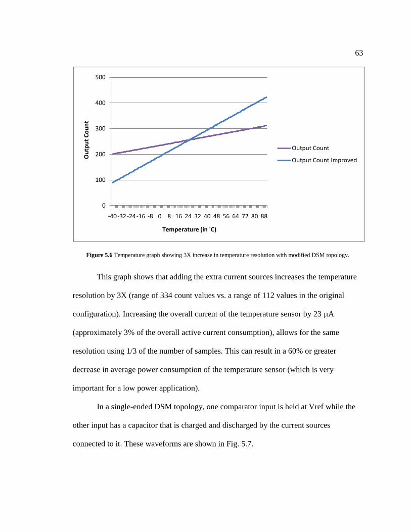
63
Figure 5.6 Temperature graph showing 3X increase in temperature resolution with modified DSM topology.
This graph shows that adding the extra current sources increases the temperature
resolution by 3X (range of 334 count values vs. a range of 112 values in the original
configuration). Increasing the overall current of the temperature sensor by 23 µA
(approximately 3% of the overall active current consumption), allows for the same
resolution using 1/3 of the number of samples. This can result in a 60% or greater
decrease in average power consumption of the temperature sensor (which is very
important for a low power application).
In a single-ended DSM topology, one comparator input is held at Vref while the
other input has a capacitor that is charged and discharged by the current sources
connected to it. These waveforms are shown in Fig. 5.7.
0
100
200
300
400
500
-40-32-24-16 -8 0 8 16 24 32 40 48 56 64 72 80 88
Ou
tpu
t C
ou
nt
Temperature (in 'C)
Output Count
Output Count Improved
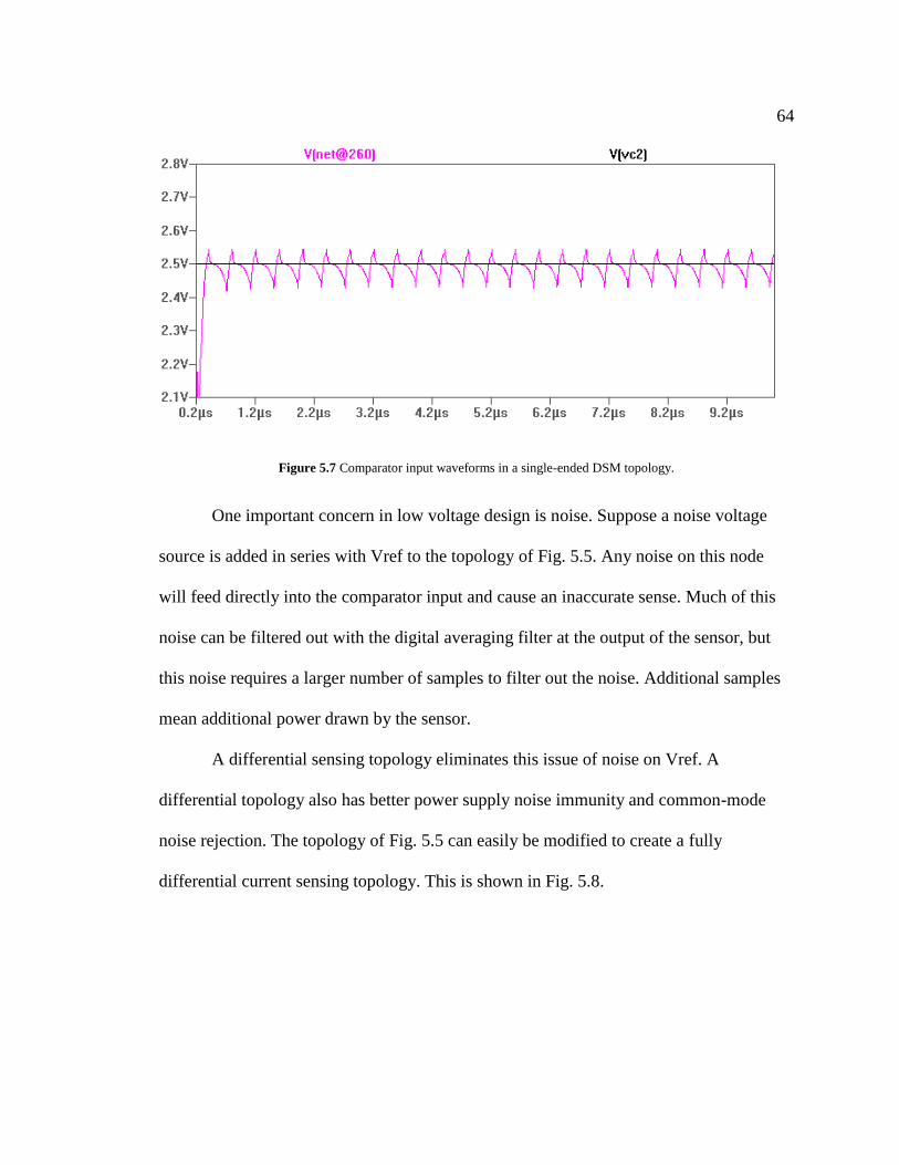
64
Figure 5.7 Comparator input waveforms in a single-ended DSM topology.
One important concern in low voltage design is noise. Suppose a noise voltage
source is added in series with Vref to the topology of Fig. 5.5. Any noise on this node
will feed directly into the comparator input and cause an inaccurate sense. Much of this
noise can be filtered out with the digital averaging filter at the output of the sensor, but
this noise requires a larger number of samples to filter out the noise. Additional samples
mean additional power drawn by the sensor.
A differential sensing topology eliminates this issue of noise on Vref. A
differential topology also has better power supply noise immunity and common-mode
noise rejection. The topology of Fig. 5.5 can easily be modified to create a fully
differential current sensing topology. This is shown in Fig. 5.8.
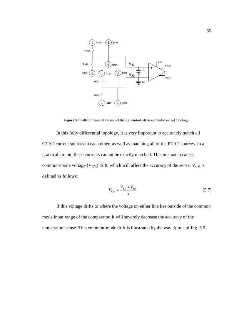
65
Figure 5.8 Fully differential version of the Kelvin-to-Celsius (extended range) topology.
In this fully differential topology, it is very important to accurately match all
CTAT current sources to each other, as well as matching all of the PTAT sources. In a
practical circuit, these currents cannot be exactly matched. This mismatch causes
common-mode voltage (VCM) drift, which will affect the accuracy of the sense. VCM is
defined as follows:
2
10 BB
CM
VVV
(5.7)
If this voltage drifts to where the voltage on either line lies outside of the common
mode input range of the comparator, it will severely decrease the accuracy of the
temperature sense. This common-mode drift is illustrated by the waveforms of Fig. 5.9.
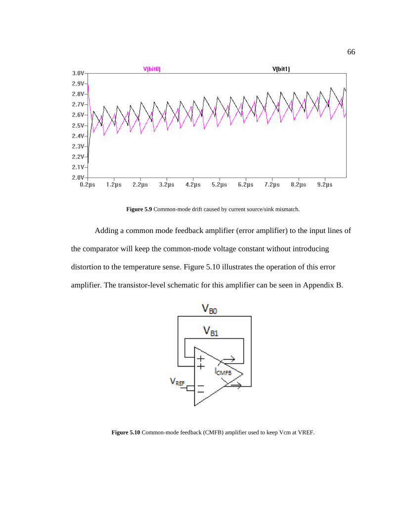
66
Figure 5.9 Common-mode drift caused by current source/sink mismatch.
Adding a common mode feedback amplifier (error amplifier) to the input lines of
the comparator will keep the common-mode voltage constant without introducing
distortion to the temperature sense. Figure 5.10 illustrates the operation of this error
amplifier. The transistor-level schematic for this amplifier can be seen in Appendix B.
Figure 5.10 Common-mode feedback (CMFB) amplifier used to keep Vcm at VREF.
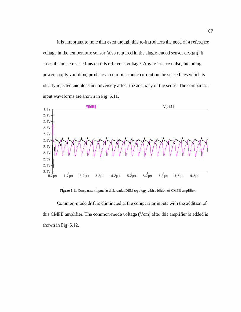
67
It is important to note that even though this re-introduces the need of a reference
voltage in the temperature sensor (also required in the single-ended sensor design), it
eases the noise restrictions on this reference voltage. Any reference noise, including
power supply variation, produces a common-mode current on the sense lines which is
ideally rejected and does not adversely affect the accuracy of the sense. The comparator
input waveforms are shown in Fig. 5.11.
Figure 5.11 Comparator inputs in differential DSM topology with addition of CMFB amplifier.
Common-mode drift is eliminated at the comparator inputs with the addition of
this CMFB amplifier. The common-mode voltage (Vcm) after this amplifier is added is
shown in Fig. 5.12.
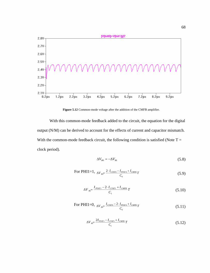
68
Figure 5.12 Common-mode voltage after the addition of the CMFB amplifier.
With this common-mode feedback added to the circuit, the equation for the digital
output (N/M) can be derived to account for the effects of current and capacitor mismatch.
With the common-mode feedback circuit, the following condition is satisfied (Note T =
clock period).
10 BB VV (5.8)
For PHI1=1, T
C
IIIV CMFBPTATCTAT
B
0
000
2
(5.9)
TC
IIIV CMFBCTATPTAT
B
1
11
1
2 (5.10)
For PHI1=0, T
C
IIIV CMFBPTATCTAT
B
0
000
2
(5.11)
TC
IIIV CMFBCTATPTAT
B
1
111
2
(5.12)
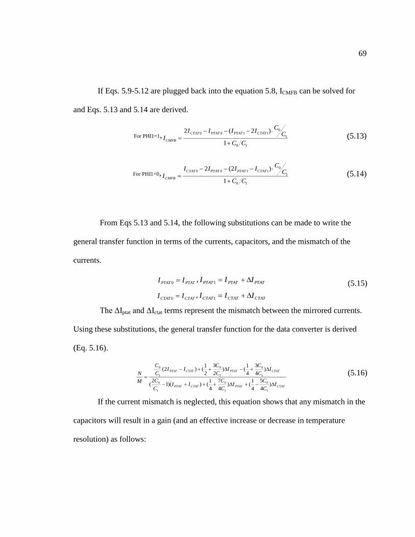
69
If Eqs. 5.9-5.12 are plugged back into the equation 5.8, ICMFB can be solved for
and Eqs. 5.13 and 5.14 are derived.
For PHI1=1,10
1
01100
1
)2(2
CC
CC
IIIII
CTATPTATPTATCTAT
CMFB
(5.13)
For PHI1=0,10
1
01100
1
)2(2
CC
CC
IIIII
CTATPTATPTATCTAT
CMFB
(5.14)
From Eqs 5.13 and 5.14, the following substitutions can be made to write the
general transfer function in terms of the currents, capacitors, and the mismatch of the
currents.
PTATPTAT II 0,
PTATPTATPTAT III 1
CTATCTAT II 0,
CTATCTATCTAT III 1
(5.15)
The ΔIptat and ΔIctat terms represent the mismatch between the mirrored currents.
Using these substitutions, the general transfer function for the data converter is derived
(Eq. 5.16).
CTATPTATCTATPTAT
CTATPTATCTATPTAT
IC
CI
C
CII
C
C
IC
CI
C
CII
C
C
M
N
)4
5
4
1()
4
7
4
1())(1
2(
)4
3
4
1()
2
3
2
1()2(
1
0
1
0
1
0
1
0
1
0
1
0
(5.16)
If the current mismatch is neglected, this equation shows that any mismatch in the
capacitors will result in a gain (and an effective increase or decrease in temperature
resolution) as follows:

70
))(2(
2
0
1CTATPTAT
CTATPTAT
IIC
C
II
M
N
(5.17)
Programming with metal, fuses, or some type of mode register when the sensor is
integrated into a given application would be desirable to adjust the gain of the sensor (and
thus the temperature resolution).
Finally, if the capacitor gain is set to 1, the current mismatch adversely affects the
linearity adding a constant term to both the numerator and denominator of the transfer
function:
CTATPTATCTATPTAT
CTATPTATCTATPTAT
IIII
IIII
M
N
2
22
(5.18)
5.4 Mixed-Signal Design Issues
The fully differential DSM temperature sensor was designed using models for the
AMI C5 process and was then fabricated in that process through the MOSIS Fabrication
Organization [14]. A single-ended DSM sensor was also designed and laid out on the
same chip to help compare a fully differential topology to a single-ended topology. The
full-chip schematics are contained in Appendix B.
The full-chip layout of the sensor test chip is shown below in Fig. 5.13.
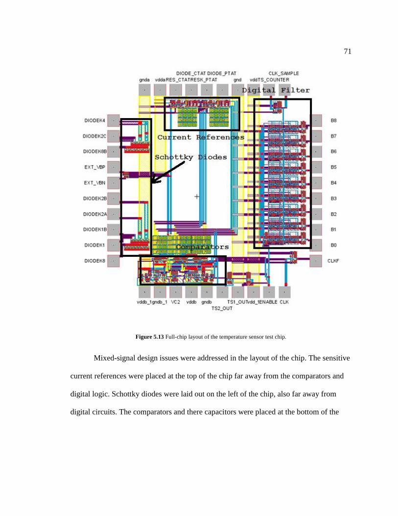
71
Figure 5.13 Full-chip layout of the temperature sensor test chip.
Mixed-signal design issues were addressed in the layout of the chip. The sensitive
current references were placed at the top of the chip far away from the comparators and
digital logic. Schottky diodes were laid out on the left of the chip, also far away from
digital circuits. The comparators and there capacitors were placed at the bottom of the
72
chip, and the digital averaging filter (ones counter) was placed at the far right of the chip
for maximum noise isolation.
Three separate power supply domains were also used to improve noise immunity.
These domains are shown in Table 5.1.
Table 5.1 Power supply domains used to improve noise performance.
Another important layout issue is minimizing the input-referred offset of the
differential amplifiers used in the current reference circuits. A common centroid layout
configuration was used with these differential amplifiers to minimize this offset. Figures
4.5 and 4.6 showed that variation in this offset will cause variation in the absolute value
of the reference currents. The equation for the output code of the temperature sensor (5.6)
shows that variation in these current values will directly affect the slope of the
temperature curve, which causes a gain error. This is why a common centroid layout
configuration is used for these amplifiers. The pre-amplifier for the comparator does not
need to use this layout configuration, since the sensor accuracy will not be affected by
input offset on the comparator.
The concept of a common centroid layout is shown in Fig. 5.14, with A and B
representing the input differential pair of an amplifier. All blocks labeled the same are
connected in parallel.
Power Supply Domain Description Circuits in Domain
vdd, gnd Digital supply Digital filter, clocking logic
vdda, gnda Sensitive analog supply Current references, Schottky diodes
vddb, gndb Noisy analog supply Comparators, associated circuits
73
Figure 5.14 Diagram showing the common centroid concept for improved element matching.
Finally, resistors were not fabricated on this chip. Instead, the resistor connections
are made off-chip to make the trimming of the references easier. The diode connections
were also made configurable to facilitate reference trimming.
5.5 Simulation Results
The differential temperature sensor was simulated thoroughly to evaluate
linearity, noise performance, and performance with current mismatch. Simulations were
run on the temperature sensor with ideal matching conditions and also with current
mismatch to create transfer curves for the temperature sensor and evaluate the accuracy
of the derived equations. Figs. 5.15 and 5.16 show these simulation results and the error
(differential non-linearity or DNL) introduced by ~2% current mismatch on both ICTAT
and IPTAT. Fig. 5.15 illustrates how the temperature sensor is calibrated.
A B A BB A B A
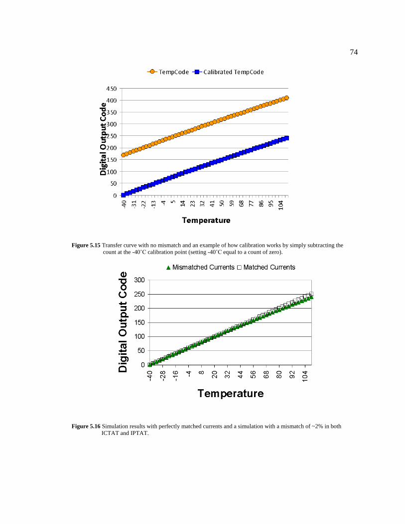
74
Figure 5.15 Transfer curve with no mismatch and an example of how calibration works by simply subtracting the
count at the -40˚C calibration point (setting -40˚C equal to a count of zero).
Figure 5.16 Simulation results with perfectly matched currents and a simulation with a mismatch of ~2% in both
ICTAT and IPTAT.
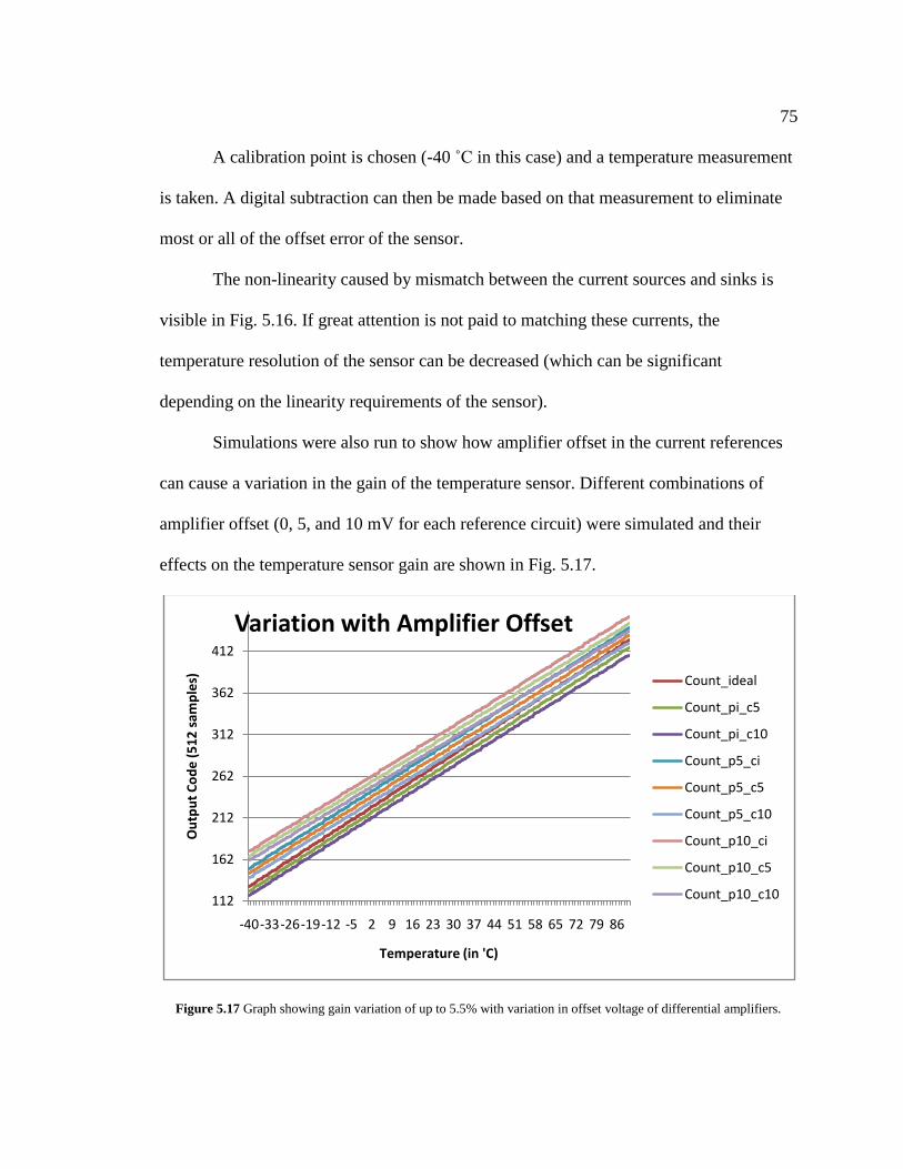
75
A calibration point is chosen (-40 ˚C in this case) and a temperature measurement
is taken. A digital subtraction can then be made based on that measurement to eliminate
most or all of the offset error of the sensor.
The non-linearity caused by mismatch between the current sources and sinks is
visible in Fig. 5.16. If great attention is not paid to matching these currents, the
temperature resolution of the sensor can be decreased (which can be significant
depending on the linearity requirements of the sensor).
Simulations were also run to show how amplifier offset in the current references
can cause a variation in the gain of the temperature sensor. Different combinations of
amplifier offset (0, 5, and 10 mV for each reference circuit) were simulated and their
effects on the temperature sensor gain are shown in Fig. 5.17.
Figure 5.17 Graph showing gain variation of up to 5.5% with variation in offset voltage of differential amplifiers.
112
162
212
262
312
362
412
-40-33-26-19-12 -5 2 9 16 23 30 37 44 51 58 65 72 79 86
Ou
tpu
t C
od
e (
51
2 s
amp
les)
Temperature (in 'C)
Variation with Amplifier Offset
Count_ideal
Count_pi_c5
Count_pi_c10
Count_p5_ci
Count_p5_c5
Count_p5_c10
Count_p10_ci
Count_p10_c5
Count_p10_c10

76
Simulation results show temperature slopes varying from 2.14 counts/˚C to 2.27
counts/˚C. This type of gain variation can be significant, which is why great care should
be taken to eliminate or at least minimize the input offset voltage of the amplifiers used in
generating PTAT and CTAT currents.
An important design objective for this temperature sensor is to have minimal
impact to the power budget in its target application. The design target used in this work
was an average current consumption of less than 1 µA. The sensor was simulated across
the temperature range of interest (-40 ˚C to 90 ˚C) and a worst-case power consumption
of 800 µA was measured. In order to keep the average current below 1 µA, this means
that the temperature sensor cannot be turned on for more than 1.2 ms/s. If a clock
frequency of 10 MHz is used and 512 samples are taken during a sensing operation, then
a sensing operation will take less than 60 µs. Therefore, a sensing operation can take
place every 50 ms (1.2 ms/ 60 µs), and the average current consumption will still be kept
under 1 µA. This frequency of sensing operations is sufficient for almost any possible
application.
Finally, simulations were completed to evaluate the sensor performance with
noise on Vref and on the power supplies. While most of the noise could be filtered out on
either design with greater averaging of the comparator output for the single-ended design
(which can lead to the temperature sensor using too much power in low power
applications), the fully differential design showed much better noise performance under a
wide array of noise conditions and a smaller number of samples (32-128 samples). The
77
fully differential topology is more immune to Vref noise due to the CMFB amplifier
turning any noise on Vref into a common mode current signal injected equally onto both
sensing lines. In addition the inputs to the comparator are laid out such that any noise on
either line should couple to the other line and thus be rejected from the comparator
decision.
5.6 Summary
The design of a fully differential current-mode sigma-delta temperature sensor
using Schottky diode-based references has been discussed. The design methodology has
been presented with special attention given to the advantages of using a fully differential,
noise shaping data converter topology and current references using Schottky diodes (as
opposed to diode-connected PNP transistors). This sensor was designed using the AMI
0.5 µm process through a MOSIS fabrication organization [14], and the chip performance
will be evaluated and compared to the simulated results in chapter 6.
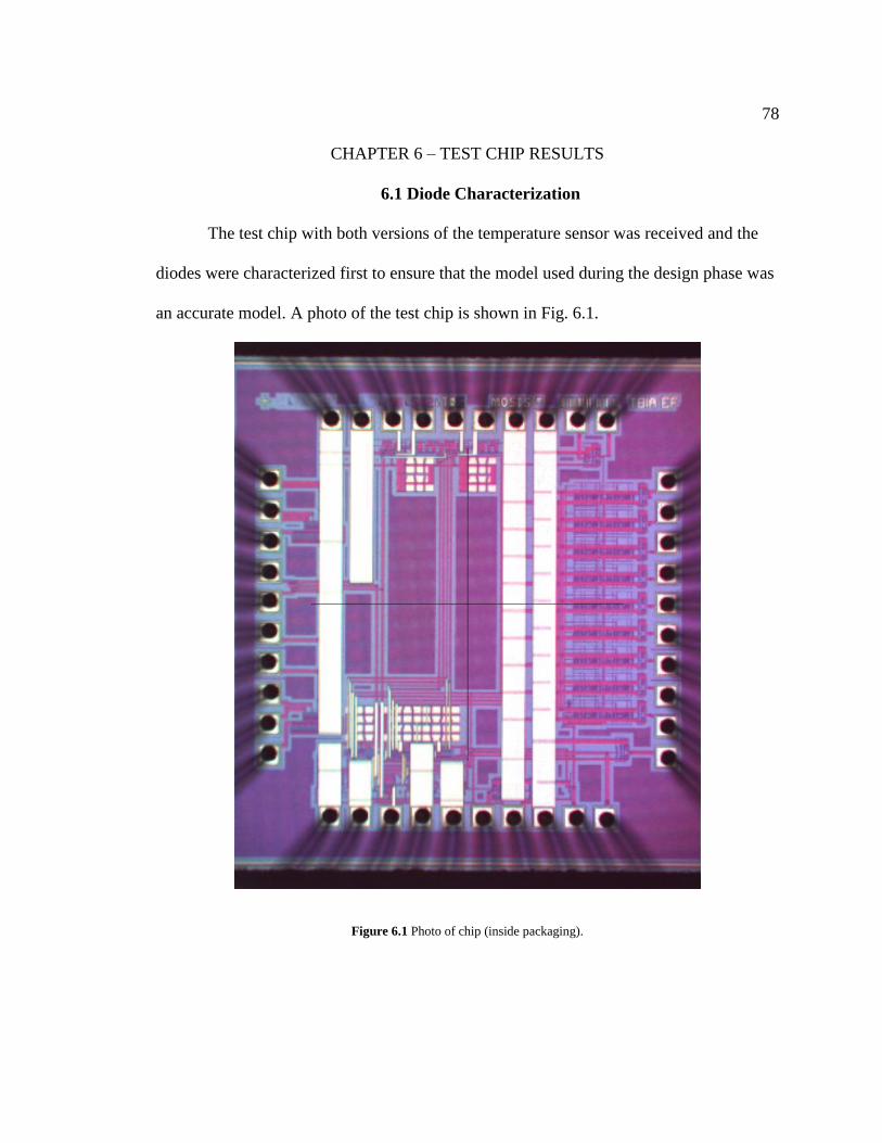
78
CHAPTER 6 – TEST CHIP RESULTS
6.1 Diode Characterization
The test chip with both versions of the temperature sensor was received and the
diodes were characterized first to ensure that the model used during the design phase was
an accurate model. A photo of the test chip is shown in Fig. 6.1.
Figure 6.1 Photo of chip (inside packaging).
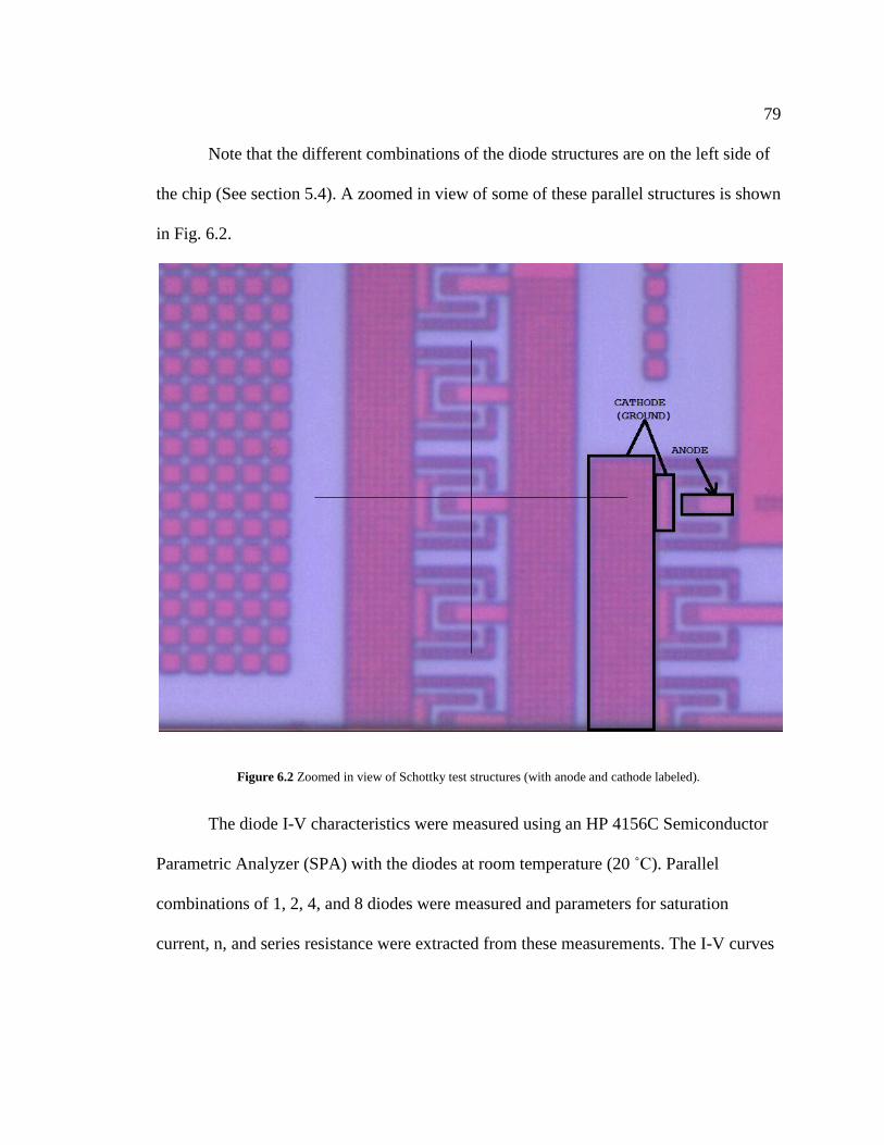
79
Note that the different combinations of the diode structures are on the left side of
the chip (See section 5.4). A zoomed in view of some of these parallel structures is shown
in Fig. 6.2.
Figure 6.2 Zoomed in view of Schottky test structures (with anode and cathode labeled).
The diode I-V characteristics were measured using an HP 4156C Semiconductor
Parametric Analyzer (SPA) with the diodes at room temperature (20 ˚C). Parallel
combinations of 1, 2, 4, and 8 diodes were measured and parameters for saturation
current, n, and series resistance were extracted from these measurements. The I-V curves
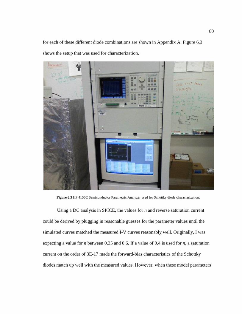
80
for each of these different diode combinations are shown in Appendix A. Figure 6.3
shows the setup that was used for characterization.
Figure 6.3 HP 4156C Semiconductor Parametric Analyzer used for Schottky diode characterization.
Using a DC analysis in SPICE, the values for n and reverse saturation current
could be derived by plugging in reasonable guesses for the parameter values until the
simulated curves matched the measured I-V curves reasonably well. Originally, I was
expecting a value for n between 0.35 and 0.6. If a value of 0.4 is used for n, a saturation
current on the order of 3E-17 made the forward-bias characteristics of the Schottky
diodes match up well with the measured values. However, when these model parameters
81
were used to derive the value for the resistor in the PTAT current source (see Tables 4.1,
and 4.2 with the associated discussion), the simulated value underestimated the measured
value of the the PTAT current by almost 400%! The new parameters for the Schottky
diode model were re-derived through the iterative simulation process and the new values
were derived as follows: n = 1.65, rs = 400 ohms, and Isat = 1E-8 A.
Another important parameter to determine for the diode is the diode voltage
change with temperature (dVD/dT). This quantity is used directly in the equation to
design the CTAT current source. In [13], this value was determined to be -0.56 mV/˚C.
Unfortunately, no temperature control mechanism was available in a convenient location
to the SPA that was used to characterize the diodes. Instead, this parameter was
determined after characterizing the CTAT current source using a Schottky diode.
Essentially identical results were obtained for the diodes in this process run, and a value
of -0.55 mV/˚C was used for this design. In order to make the SPICE model match up
reasonably, the “EG” (activation energy) parameter of the Schottky diode model was set
to 0.40.
After the diodes were characterized, the model parameters were plugged into
SPICE and the resistor values were calculated for the PTAT and CTAT current sources.
This is discussed in the next section.
6.2 Current Source Characterization
After the diodes were characterized, the SPICE diode model was modified and the
current sources were redesigned. Plugging the value of n = 1.65 into Eq. 4.5, the value of
82
R = 8.7 Kohms for a PTAT current of 10 µA at 25 ˚C. The resistor for a CTAT current of
10 µA was determined to be 28 Kohms. The current sources were then connected and
characterized on all five chips to determine the variation in diode parameters across the
different test chips. In order to obtain a CTAT current of 10 µA on all chips (one chip
sustained ESD damage, so four chips were actually characterized instead of all five), the
resistor value needed to be trimmed from 22 Kohms to 36 Kohms. This indicates a pretty
significant variation in saturation current from die to die. The resistors to obtain PTAT
currents of 10 µA only varied from 7.8 Kohms to 9 Kohms. This indicates that the
measured value for n does not vary too much from die to die.
6.3 Temperature Sensor characterization
Both the differential and single-ended designs were connected and characterized
using a thermal chamber to vary the temperature from 40 ˚C up to approximately 85 ˚C.
Unfortunately, the thermal chamber available for characterization of this device could not
be controlled very precisely (the exact temperature was difficult to control precisely).
However, the relative temperature change in the chamber could be controlled with pretty
good accuracy.
A pin diagram of the test chip is shown in Fig. 6.4.
83
a11
a22
3a3
4a4
b1
b2
b3
b4
5
6
7
8
a11
a22
3a3
4a4
b1
b2
b3
b4
5
6
7
8
a11
a22
3a3
4a4
b1
b2
b3
b4
5
6
7
8
a11
a22
3a3
4a4
b1
b2
b3
b4
5
6
7
8
a11
a22
3a3
4a4
b1
b2
b3
b4
5
6
7
8
B4
B5
B6
B7
B8
CLK_SAMPLE
TS_COUNTER
VDD
GND
DIODE_PTAT
RESK_PTAT
DIODE_CTAT
RES_CTAT
VDDA
GNDA
DIODEK4
DIODEK2C
DIODEK8B
EXT_VBP
EXT_VBN
B3
B2
B1
B0
CLKF
CLK
ENABLE
VDD
TS1_OUT
TS2_OUT
GNDB
VDDB
VC2
GNDB
VDDB
DIODEK8
DIODEK1
DIODEK1B
DIODEK2A
DIODEK2B
Figure 6.4 Pinout diagram for the temperature sensor test chip.
A table describing the purpose of each of the pin connections is shown below.
84
Table 6.1 Pin list for Temp Sensor test chip.
Pin number Pin name Pin Description
1 B4 Counter output Bit 4
2 B5 Counter output Bit 5
3 B6 Counter output Bit 6
4 B7 Counter output Bit 7
5 B8 Counter output Bit 8
6 CLK_SAMPLE Sampling Clock for digital counter
7 TS_COUNTER Counter input (from DSM outputs)
8 VDD Digital power
9 GND Digital ground
10 DIODE_PTAT PTAT diode connection
11 RESK_PTAT PTAT resistor/diode series connection
12 DIODE_CTAT CTAT diode connection
13 RES_CTAT CTAT resistor connection
14 VDDA Analog power
15 GNDA Analog ground
16 DIODEK4 Four Schottky diode parallel combo.
17 DIODEK2C Two Schottky diode parallel combo.
18 DIODEK8B Eight Schottky diode parallel combo.
19 EXT_VBP Resistor connection to bias PMOS diff amps.
20 EXT_VBN Resistor connection to bias NMOS diff amps.
21 B3 Counter output Bit 3
22 B2 Counter output Bit 2
23 B1 Counter output Bit 1
24 B0 Counter output Bit 0
25 CLKF Inverted version of CLK input (this is an output).
26 CLK CLK input
27 ENABLE Enable/RST_ input
28 VDD Digital power
29 TS1_OUT Differential DSM comparator output.
30 TS2_OUT Single-ended DSM comparator output.
31 GNDB Wide-swing analog ground.
32 VDDB Wide-swing analog power.
33 VC2 Sensor reference voltage (nominally VDD/2)
34 GNDB Wide-swing analog ground.
35 VDDB Wide-swing analog power.
36 DIODEK8 Eight Schottky diode parallel combo.
37 DIODEK1 Single Schottky diode.
38 DIODEK1B Single Schottky diode.
39 DIODEK2A Two Schottky diode parallel combo.
40 DIODEK2B Two Schottky diode parallel combo.
85
To put the chip in test configuration, all power supplies were connected to an HP
E3631A DC power supply. Two Agilent arbitrary waveform generators were used in
burst modulation mode to generate the reset pulse (ENABLE) and sampling clock (CLK)
for the sensor. CLKF was then connected externally to the CLK_SAMPLE input of the
ones counter (digital averaging filter). The TS1_OUT and TS2_OUT pins were
connected one at a time to the TS_COUNTER input (depending on which sensor was
being characterized). Biasing resistors of 360 Kohms were used to bias the differential
amplifiers on the test chip. The 8.7 Kohm and 28 Kohm resistors were then connected to
the RES_CTAT and RESK_PTAT pins to bias the current references. The appropriate
diode connections were also connected externally to correctly bias the current references.
The unused diode combinations were connected to ground.
In order to ease the collection of data in the thermal chamber, an R2R ladder was
connected to the 6 MSBs of the counter output to be able to get an analog value that can
be measured using a digital multimeter that corresponds to the digital output code of the
averaging filter. After the design was validated outside of a thermal chamber, the test
board was placed in the thermal chamber and the temperature was varied to collected data
across a desired temperature sensor. Figure 6.5 shows this test circuit wired together on a
breadboard.
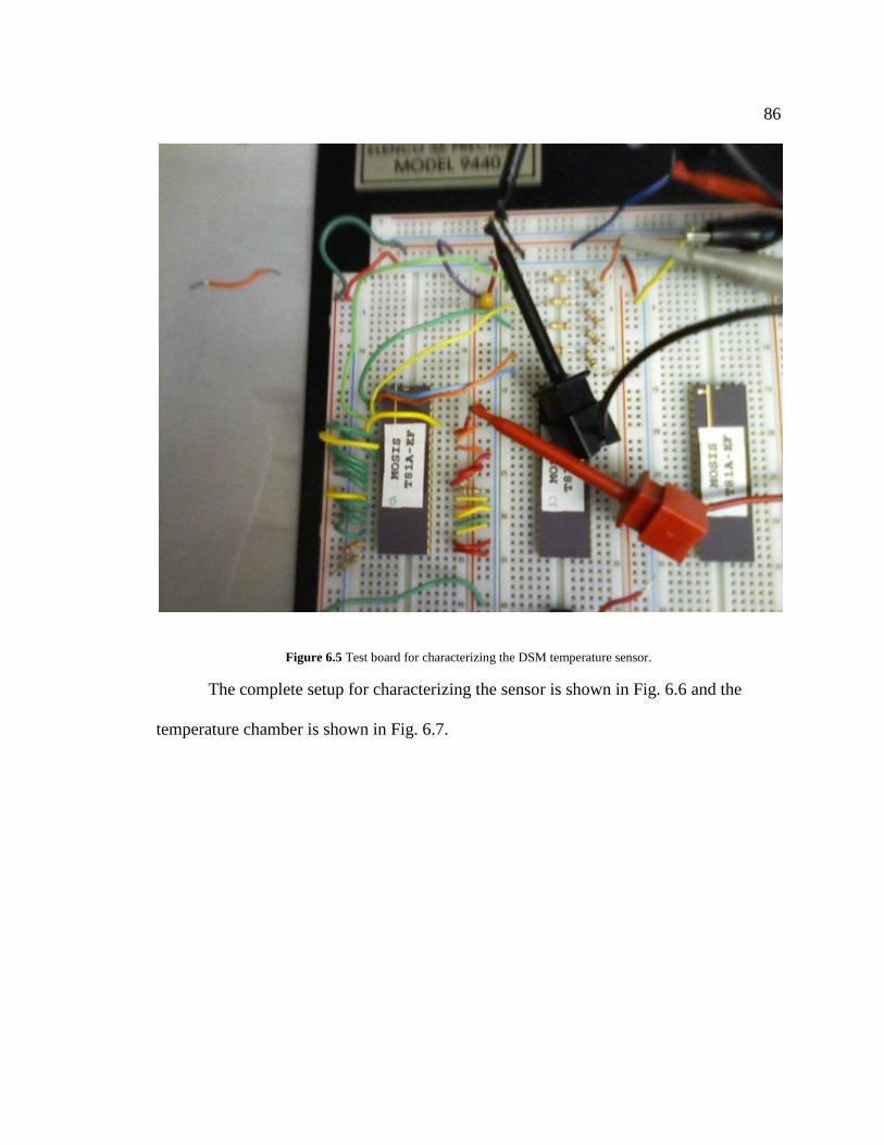
86
Figure 6.5 Test board for characterizing the DSM temperature sensor.
The complete setup for characterizing the sensor is shown in Fig. 6.6 and the
temperature chamber is shown in Fig. 6.7.
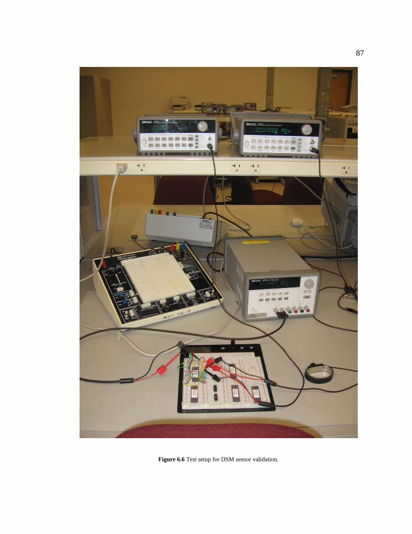
87
Figure 6.6 Test setup for DSM sensor validation.
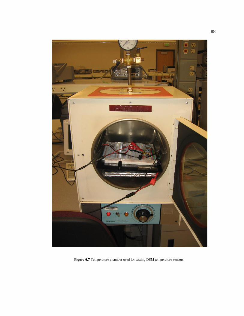
88
Figure 6.7 Temperature chamber used for testing DSM temperature sensors.
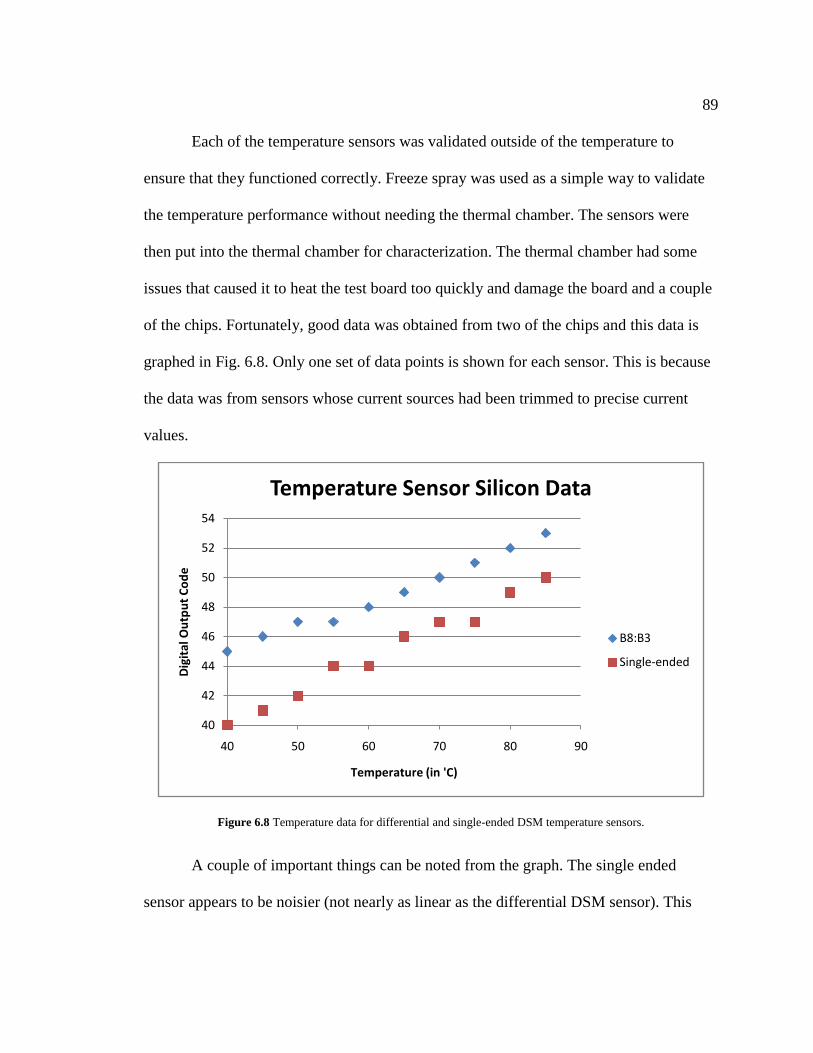
89
Each of the temperature sensors was validated outside of the temperature to
ensure that they functioned correctly. Freeze spray was used as a simple way to validate
the temperature performance without needing the thermal chamber. The sensors were
then put into the thermal chamber for characterization. The thermal chamber had some
issues that caused it to heat the test board too quickly and damage the board and a couple
of the chips. Fortunately, good data was obtained from two of the chips and this data is
graphed in Fig. 6.8. Only one set of data points is shown for each sensor. This is because
the data was from sensors whose current sources had been trimmed to precise current
values.
Figure 6.8 Temperature data for differential and single-ended DSM temperature sensors.
A couple of important things can be noted from the graph. The single ended
sensor appears to be noisier (not nearly as linear as the differential DSM sensor). This
40
42
44
46
48
50
52
54
40 50 60 70 80 90
Dig
ital
Ou
tpu
t C
od
e
Temperature (in 'C)
Temperature Sensor Silicon Data
B8:B3
Single-ended
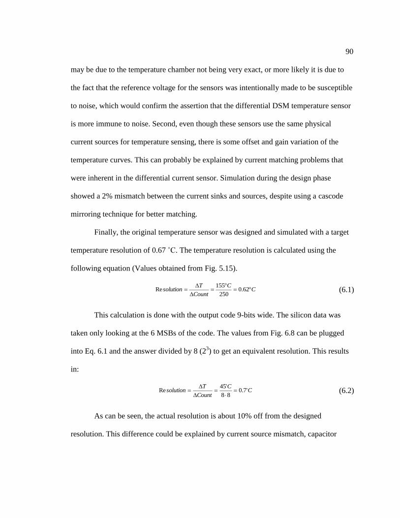
90
may be due to the temperature chamber not being very exact, or more likely it is due to
the fact that the reference voltage for the sensors was intentionally made to be susceptible
to noise, which would confirm the assertion that the differential DSM temperature sensor
is more immune to noise. Second, even though these sensors use the same physical
current sources for temperature sensing, there is some offset and gain variation of the
temperature curves. This can probably be explained by current matching problems that
were inherent in the differential current sensor. Simulation during the design phase
showed a 2% mismatch between the current sinks and sources, despite using a cascode
mirroring technique for better matching.
Finally, the original temperature sensor was designed and simulated with a target
temperature resolution of 0.67 ˚C. The temperature resolution is calculated using the
following equation (Values obtained from Fig. 5.15).
CC
Count
Tsolution
62.0
250
155Re (6.1)
This calculation is done with the output code 9-bits wide. The silicon data was
taken only looking at the 6 MSBs of the code. The values from Fig. 6.8 can be plugged
into Eq. 6.1 and the answer divided by 8 (23) to get an equivalent resolution. This results
in:
CC
Count
Tsolution '7.0
88
'45Re
(6.2)
As can be seen, the actual resolution is about 10% off from the designed
resolution. This difference could be explained by current source mismatch, capacitor

91
mismatch, or perhaps another reason. This value still achieves the desired resolution of
better than 1 ˚C for the temperature sensor.
92
CHAPTER 7 – CONCLUSIONS AND FUTURE WORK
7.1 Conclusions
The design of a fully differential DSM temperature sensor using Schottky diode-
based references has been presented in this work. The sensor was designed to achieve
better than 1 ˚C of temperature resolution, which is suitable for almost any application of
an integrated CMOS temperature sensor. Special attention has been given to the
integration of Schottky diode-based current references into the design in order to achieve
lower-voltage operation when the design is implemented in an advanced CMOS process
(with VDD=1V or lower). The Schottky diode-based references have more variation than
those designed with PN junction diodes (due to greater variation in the Schottky diode
characteristics), but the problem is shown to be manageable through trimming the current
reference with fuse or programmable register trims.
The DSM current sensing architecture was chosen because of its ability to achieve
high resolution by using an averaging filter (digital lowpass filter) on the output of the
circuit. A fully differential current sensing architecture was developed from the single-
ended architecture and was shown to have better immunity to power supply and reference
voltage noise. A temperature sensing architecture to improve the temperature resolution
has been explained and shown the potential to reduce average power consumption of the
sensor (important in low-power applications).
The main drawback to the fully differential design is the difficulty in match
currents that are both sourced and sunk. The impact is minimized through careful design,
93
but may limit the sensor resolution compared to a single-ended design. The differential
temperature sensor appears to have a clear advantage over a single-ended design in low
resolution (6 bits or less), low power, and/or noisy applications due to its greater
immunity to noise.
7.2 Future Work
Some important areas of this research that could be explored in the future include
improved current mirroring techniques (to improve matching of sourced/sunk currents),
application of high resolution temperature sensing to novel technologies (such as thermal
memory, for instance), and developing higher order DSM temperature sensing
architectures. Also, in order to improve the linear behavior of the Schottky diodes across
temperature (VD is treated as a linearly decreasing value with temperature when
designing, which is not the case in reality), curvature correction techniques to improve
the die-to-die variation in current references could be explored for Schottky diode-based
references.
In signal processing applications, higher-order sigma-delta modulators are often
used to increase the signal-to-noise ratio (SNR) of a digital signal. This is because higher
order modulators increase the filtering of the quantization noise of the converter, which
increases the effective resolution of the modulator output. This eases the requirements on
the digital filter at the modulator output to achieve a given resolution. Higher order DSM
topologies may be required to increase the effective temperature resolution in
applications requiring ultra-fine temperature resolution.
94
Curvature correction is a technique often used to linearize the temperature
behavior of the diode voltage in high-precision current and voltage reference designs that
use PNP bipolar transistors for biasing. This is accomplished by applying a small
correction voltage to the base of the transistor (instead of leaving it connected in the
diode configuration shown in chapters 3 and 4). This same technique could be extended
to Schottky diode-based designs. This is accomplished by separating the cathode of the
Schottky diode from the bulk to enable separate control of the three terminals. This
technique was not within the scope of the project, but could be used to improve the
linearity of the temperature sense by improving the linearity of the reference currents
used in the temperature sensor.
95
WORKS CITED
[1] Rabii, Shahriar and Wooley, Bruce A, Design of Low-Voltage Low-Power Sigma-
Delta Modulators, Kluwer Academic Publishers, 1999, ISBN 0-7923-8361-3.
[2] Bakker, Anton and Huijsing, Johan, High-Accuracy CMOS Smart Temperature
Sensors, Kluwer Academic Publishers, 2000, ISBN 0-7923-7217-4.
[3] Duarte, David E., et al, “Temperature Sensor Design in a High Volume
Manufacturing 65nm CMOS Digital Process,” IEEE Custom Integrated Circuits
Conference, pp. 221-224, 2007.
[4] Baker, R. Jacob, CMOS Circuit Design, Layout, and Simulation, 2nd
Edition, IEEE
Press, 2005, ISBN 0-471-70055-X.
[5] Chen, Poki, et al, “A time-to-digital-converter-based CMOS smart temperature
sensor,” IEEE Journal of Solid-State Circuits, vol. 40, no. 8, pp. 1642-1648, August,
2005.
[6] Baker, R. Jacob, CMOS Mixed-Signal Circuit Design, IEEE Press, 2002, ISBN 0-471-
22754-4.
[7] Bakker, A., Pertjis, M. A. P. and Huijsing, J. H., A second-order sigma-delta ADC
using MOS capacitors for smart sensor applications [smart temperature sensor], IEEE
Press, 2004. ISBN 0-7803-8692-2.
[8] Streetman, Ben G. and Banerjee, Sanjay, Solid State Electronic Devices, 5th
Edition,
Prentice Hall Inc., 2000, ISBN 0-13-025538-6.
[9] Engelhart, Mike. LTSpice/Switcher CadIII Help manual. s.l. : Linear Technology,
2008.
[10] University of California at Berkeley, SPICE Overview, Department of Electrical
Engineering and Computer Science, [Online] 2008, [Cited: May 2, 2008.]
http://bwrc.eecs.berkeley.edu/Classes/icBook/SPICE/UserGuide/overview_fr.html.
[11] Hazdi-Vukovic, J, et al, Si and SiC Schottky diodes in smart power circuits, vol. 10,
Institute of Physics Publishing, 2005.
[12] Enz, C.C. and Temes, G.C., “Circuit Techniques for Reducing the Effects of Op-
Amp Imperfections: Autozeroing, Correlated Double Sampling, and Chopper
Stabilization,” Proceedings of the IEEE, vol. 84, no. 11, pp. 1584-1614, November 1996.

96
[13] Butler, David L. and Baker, R. Jacob, “Low-Voltage Bandgap Reference Design
Utilizing Schottky Diodes” IEEE Midwest Symposium on Circuits and Systems, 2005.
[14] MOSIS “Low-Cost Prototyping and Small-Volume Production Service”
http://www.mosis.org/.

97
APPENDIX A
Diode I-V Curves Measured from Diode Test Structures
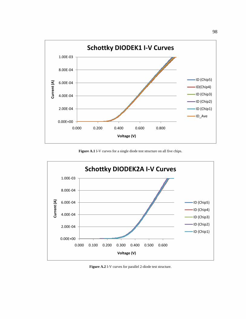
98
Figure A.1 I-V curves for a single diode test structure on all five chips.
Figure A.2 I-V curves for parallel 2-diode test structure.
0.00E+00
2.00E-04
4.00E-04
6.00E-04
8.00E-04
1.00E-03
0.000 0.200 0.400 0.600 0.800
Cu
rre
nt
(A)
Voltage (V)
Schottky DIODEK1 I-V Curves
ID (Chip5)
ID(Chip4)
ID (Chip3)
ID (Chip2)
ID (Chip1)
ID_Ave
0.00E+00
2.00E-04
4.00E-04
6.00E-04
8.00E-04
1.00E-03
0.000 0.100 0.200 0.300 0.400 0.500 0.600
Cu
rre
nt
(A)
Voltage (V)
Schottky DIODEK2A I-V Curves
ID (Chip5)
ID (Chip4)
ID (Chip3)
ID (Chip2)
ID (Chip1)
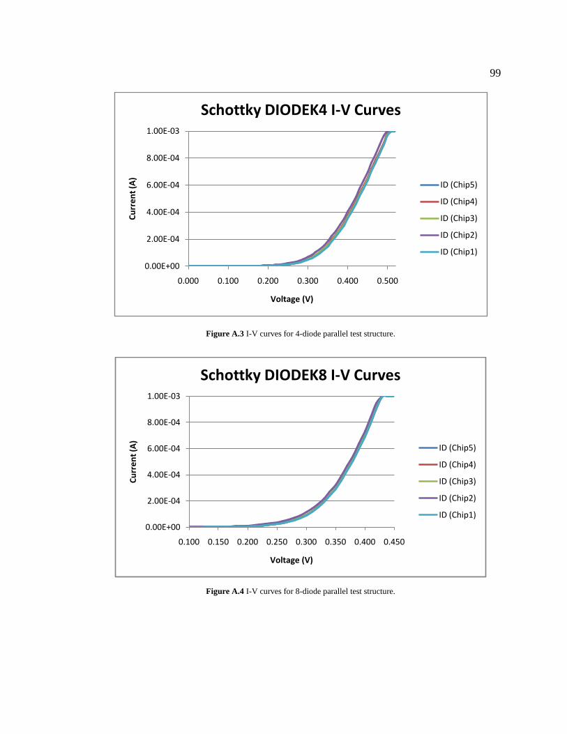
99
Figure A.3 I-V curves for 4-diode parallel test structure.
Figure A.4 I-V curves for 8-diode parallel test structure.
0.00E+00
2.00E-04
4.00E-04
6.00E-04
8.00E-04
1.00E-03
0.000 0.100 0.200 0.300 0.400 0.500
Cu
rre
nt
(A)
Voltage (V)
Schottky DIODEK4 I-V Curves
ID (Chip5)
ID (Chip4)
ID (Chip3)
ID (Chip2)
ID (Chip1)
0.00E+00
2.00E-04
4.00E-04
6.00E-04
8.00E-04
1.00E-03
0.100 0.150 0.200 0.250 0.300 0.350 0.400 0.450
Cu
rre
nt
(A)
Voltage (V)
Schottky DIODEK8 I-V Curves
ID (Chip5)
ID (Chip4)
ID (Chip3)
ID (Chip2)
ID (Chip1)

100
APPENDIX B
Key Temperature Sensor Schematics
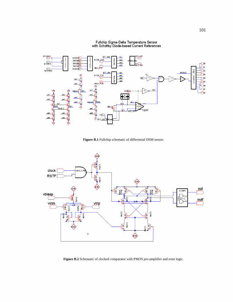
101
Figure B.1 Fullchip schematic of differential DSM sensor.
Figure B.2 Schematic of clocked comparator with PMOS pre-amplifier and reset logic.
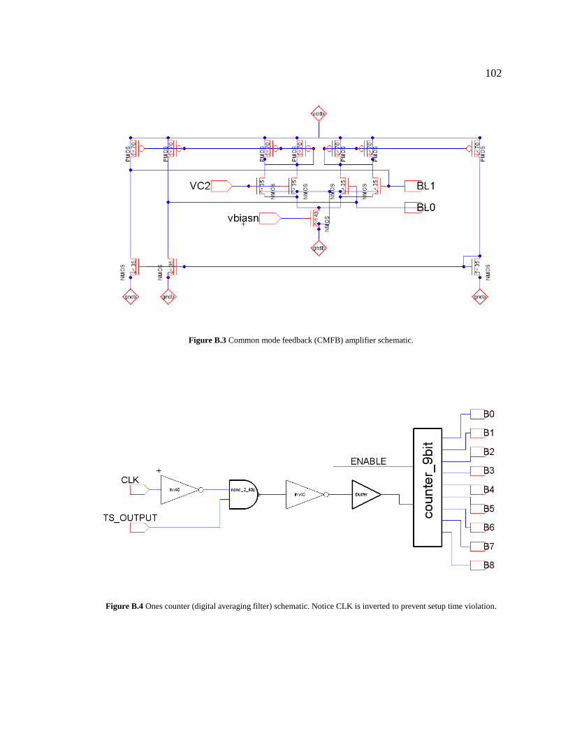
102
Figure B.3 Common mode feedback (CMFB) amplifier schematic.
Figure B.4 Ones counter (digital averaging filter) schematic. Notice CLK is inverted to prevent setup time violation.