low dropout cmos voltage regulator s-818 … · low dropout cmos voltage regulator s-818 series ......
TRANSCRIPT

Rev.1.2
Seiko Instruments Inc. 1
LOW DROPOUT CMOS VOLTAGE REGULATOR S-818 Series
Note : Please consider power dissipation of the package when the output current is large.
Packagey 5-pin SOT-23-5 (Package drawing code: MP005-A)y 5-pin SOT-89-5 (Package drawing code: UP005-A)
The S-818 Series is a positive voltage regulator developedutilizing CMOS technology featured by low dropout voltage,high output voltage accuracy and low current consumption.Built-in low on-resistance transistor provides low dropoutvoltage and large output current. A ceramic capacitor of 2 µFor more can be used as an output capacitor. A power-OFFcircuit ensures long battery life.The SOT-23-5 miniaturized package and the SOT-89-5package are recommended for configuring portable devicesand large output current applications, respectively.
Applicationsy Power source for battery-powered devices
y Power source for personal communication devices
y Power source for home electric/electronicappliances
Featuresy Low current consumption During operation: Typ. 30 µA, Max. 40 µA During power off: Typ. 100 nA, Max. 500 nAy Output voltage: 0.1 V steps between 2.0 and 6.0 Vy High accuracy output voltage: ±2.0%y Peak output current;
200 mA capable (3.0 V output product, VIN=4 V) Note
300 mA capable (5.0 V output product, VIN=6 V) Note
y Low dropout voltageTyp. 170 mV (5.0 V output product, IOUT = 60 mA)
A ceramic capacitor (2 µF or more) can be used as anoutput capacitor.
y Built-in power-off circuity Compact package: SOT-23-5, SOT-89-5

LOW DROPOUT CMOS VOLTAGE REGULATOR Rev.1.2S-818 Series
2 Seiko Instruments Inc.
Block Diagram
Reference
voltage
VOUT
ON/OFF
VSS
VIN
*1: Parasitic diode
*1
ON/OFF
circuit
Figure 1 Block Diagram
Selection Guide1. Product Name
S-818x xx A xx - xxx - T2
IC orientation in taping specificationsProduct abbreviation
Package type MC : SOT-23-5UC :
A: ON/OFF pin has positive logic (high active)
B: ON/OFF pin has negative logic (low active)
SOT-89-5
Product type
Output voltage x 10
Table 1 Selection Guide
Output Voltage SOT-23-5 SOT-89-5
2.0 V ± 2.0% S-818A20AMC-BGA-T2 S-818A20AUC-BGA-T2
2.5 V ± 2.0% S-818A25AMC-BGF-T2 S-818A25AUC-BGF-T2
2.8 V ± 2.0% S-818A28AMC-BGI-T2 S-818A28AUC-BGI-T2
3.0 V ± 2.0% S-818A30AMC-BGK-T2 S-818A30AUC-BGK-T2
3.3 V ± 2.0% S-818A33AMC-BGN-T2 S-818A33AUC-BGN-T2
3.8 V ± 2.0% S-818A38AMC-BGS-T2 S-818A38AUC-BGS-T2
4.0 V ± 2.0% S-818A40AMC-BGU-T2 S-818A40AUC-BGU-T2
5.0 V ± 2.0% S-818A50AMC-BHE-T2 S-818A50AUC-BHE-T2
Note:Contact SII sales division for product with an output voltage other than thosespecified above or product type B, low active product.
Rev.1.2 LOW DROPOUT CMOS VOLTAGE REGULATOR S-818 Series
Seiko Instruments Inc. 3
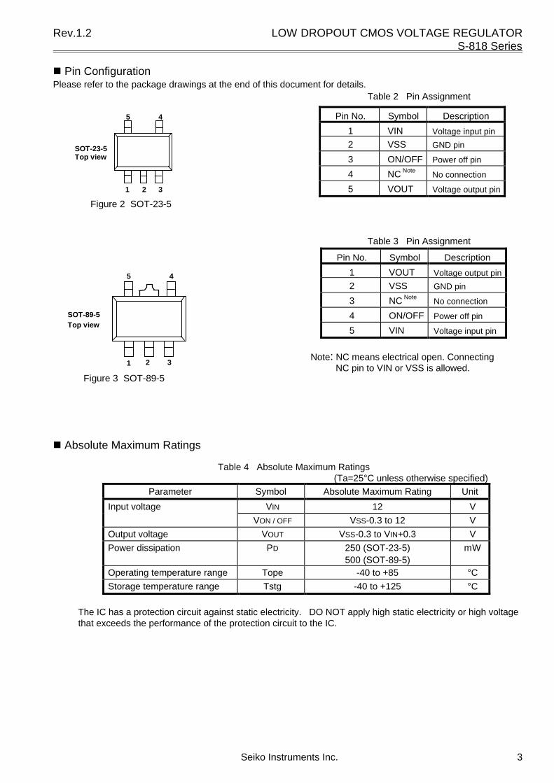
Pin ConfigurationPlease refer to the package drawings at the end of this document for details.
Table 2 Pin Assignment
Table 3 Pin Assignment
Note: NC means electrical open. ConnectingNC pin to VIN or VSS is allowed.
Absolute Maximum Ratings
Table 4 Absolute Maximum Ratings(Ta=25°C unless otherwise specified)
Parameter Symbol Absolute Maximum Rating Unit
Input voltage VIN 12 V
VON / OFF VSS-0.3 to 12 V
Output voltage VOUT VSS-0.3 to VIN+0.3 V
Power dissipation PD 250 (SOT-23-5)500 (SOT-89-5)
mW
Operating temperature range Tope -40 to +85 °CStorage temperature range Tstg -40 to +125 °C
The IC has a protection circuit against static electricity. DO NOT apply high static electricity or high voltagethat exceeds the performance of the protection circuit to the IC.
Pin No. Symbol Description
1 VIN Voltage input pin
2 VSS GND pin
3 ON/OFF Power off pin
4 NC NoteNo connection
5 VOUT Voltage output pin
Figure 2 SOT-23-5
1 32
45
SOT-23-5Top view
Pin No. Symbol Description
1 VOUT Voltage output pin
2 VSS GND pin
3 NC NoteNo connection
4 ON/OFF Power off pin
5 VIN Voltage input pin
5 4
1 32
SOT-89-5Top view
Figure 3 SOT-89-5

LOW DROPOUT CMOS VOLTAGE REGULATOR Rev.1.2S-818 Series
4 Seiko Instruments Inc.
Electrical Characteristics S-818AXXAMC/UC, S-818BXXAMC/UC
Table 5 Electrical Characteristics (Ta=25°C unless otherwise specified)
Parameter Symbol Conditions Min. Typ. Max. UnitsTest
circuits
Output voltage *1) VOUT(E) VIN=VOUT(S)+1V,IOUT=30mA VOUT(S)×0.98
VOUT(S) VOUT(S)×1.02
V 1
Output current *2) IOUT VOUT(S)+1V 2.0V ≤VOUT(S) ≤2.4V 100 *5) − − mA 3≤ VIN≤10V 2.5V ≤VOUT(S) ≤2.9V 150 *5) − − mA 3
3.0V ≤VOUT(S) ≤3.9V 200 *5) − − mA 34.0V ≤VOUT(S) ≤4.9V 250 *5) − − mA 35.0V ≤VOUT(S) ≤6.0V 300 *5) − − mA 3
Dropout voltage *3) Vdrop IOUT = 2.0V ≤VOUT(S) ≤2.4V − 0.51 0.87 V 160mA 2.5V ≤VOUT(S) ≤2.9V − 0.38 0.61 V 1
3.0V ≤VOUT(S) ≤3.4V − 0.30 0.44 V 13.5V ≤VOUT(S) ≤3.9V − 0.24 0.33 V 14.0V ≤VOUT(S) ≤4.4V − 0.20 0.26 V 14.5V ≤VOUT(S) ≤4.9V − 0.18 0.22 V 15.0V ≤VOUT(S) ≤5.4V − 0.17 0.21 V 15.5V ≤VOUT(S) ≤6.0V − 0.17 0.20 V 1
Line regulation 1 ∆VOUT1 1∆VIN • VOUT
VOUT(S) + 0.5 V ≤ VIN ≤ 10 V,IOUT = 30mA
0.05 0.2 %/V 1
Line regulation 2 ∆VOUT2 1∆VIN • VOUT
VOUT(S) + 0.5 V ≤ VIN ≤ 10 V,IOUT = 10µA
0.05 0.2 %/V 1
Load regulation ∆VOUT3 VIN = VOUT(S) + 1 V,10µA ≤ IOUT ≤ 80mA
30 50 mV 1
Output voltage temperaturecoefficient *4)
∆VOUT 1∆Ta • VOUT
VIN = VOUT(S) + 1 V, IOUT = 30mA-40°C ≤ Ta ≤ 85°C
±100 ppm/°C
1
Current consumption duringoperation
ISS1 VIN = VOUT(S) + 1 V,ON/OFF pin = ON, no load
30 40 µA 2
Current consumption whenpower off
ISS2 VIN = VOUT(S) + 1 V,ON/OFF pin = OFF, no load
0.1 0.5 µA 2
Input voltage VIN 10 V 1Power-off pin input voltage "H" VSH VIN = VOUT(S) + 1 V, RL = 1kΩ,
Judged by VOUT output level.1.5 V 4
Power-off pin input voltage "L" VSL VIN = VOUT(S) + 1 V, RL = 1kΩ,Judged by VOUT output level.
0.3 V 4
Power-off pin input current "H" ISH VIN = VOUT(S) + 1 V,ON/OFF = 7 V
0.1 µA 4
Power-off pin input current "L" ISL VIN = VOUT(S) + 1 V,ON/OFF = 0 V
-0.1 µA 4
Ripple rejection RR VIN = VOUT(S) + 1 V, f = 100Hz,∆Vrip = 0.5 V p-p, IOUT=30mA
45 dB 5
*1) VOUT(S)=Specified output voltageVOUT(E)=Effective output voltage, i.e., the output voltage at fixet IOUT(=30 mA) and input VOUT(S)+1.0 V.
*2) Output current when the output voltage goes below 95% of VOUT(E) after gradually increasing output current.*3) Vdrop = VIN1-(VOUT(E) × 0.98)
VIN1 = Input voltage when output voltage falls 98% of VOUT(E) after gradually decreasing input voltage.*4) Output voltage shift by temperature [mV/°C] is calculated using the following equation.
*5) Peak output current can exceed the minimum value.
∆VOUT [ppm/°C] ÷1000[mV/°C] = VOUT(S)[V] ×∆Ta
∆VOUT
∆Ta • VOUT
Specified output voltageOutput voltage temperature coefficient
Output voltage shift by temperature
Rev.1.2 LOW DROPOUT CMOS VOLTAGE REGULATOR S-818 Series
Seiko Instruments Inc. 5
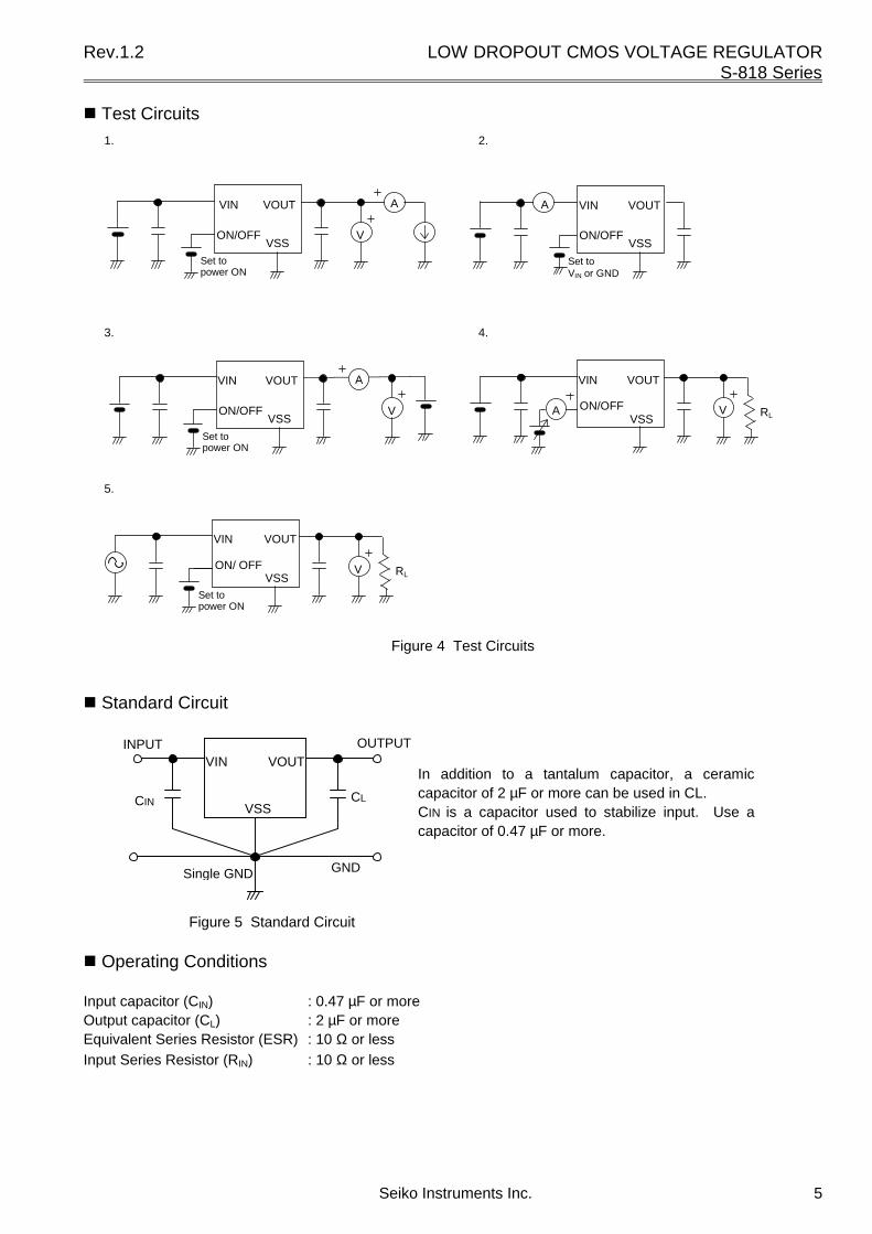
Test Circuits1. 2.
3. 4.
5.
Figure 4 Test Circuits
Standard Circuit
VSS
VOUTVIN
CIN CL
INPUT OUTPUT
GNDSingle GND
Figure 5 Standard Circuit
Operating Conditions
Input capacitor (CIN) : 0.47 µF or moreOutput capacitor (CL) : 2 µF or moreEquivalent Series Resistor (ESR) : 10 Ω or lessInput Series Resistor (RIN) : 10 Ω or less
VSS
VOUT
ON/OFF
VIN
V
A
Set topower ON
VSS
VOUT
Set toVIN or GND
ON/OFF
VINA
VSSRL
VOUT
ON/OFF
VIN
VAVSS
VOUT
ON/OFF
VIN
V
A
Set topower ON
VSS
VOUT
ON/ OFF
VIN
V
Set topower ON
RL
In addition to a tantalum capacitor, a ceramiccapacitor of 2 µF or more can be used in CL.CIN is a capacitor used to stabilize input. Use acapacitor of 0.47 µF or more.

LOW DROPOUT CMOS VOLTAGE REGULATOR Rev.1.2S-818 Series
6 Seiko Instruments Inc.
Technical Terms
1. Low dropout voltage regulatorThe low dropout voltage regulator is a voltage regulator having a low dropout voltage characteristic due to theinternal low on-resistance transistor.
2. Output voltage (VOUT)The accuracy of the output voltage is ensured at ± 2.0% under the specified conditions of input voltage,output current, and temperature, which differ product by product.
Note:When the above conditions are changed, the output voltage may vary and go out of the accuracy range ofthe output voltage. See the electrical characteristics and characteristic data for details.
3. Line regulations 1 and 2 (∆VOUT1, ∆VOUT2)Line regulation indicates the input voltage dependence of the output voltage. The value shows how much theoutput voltage changes due to the change of the input voltage when the output current is kept constant.
4. Load regulation (∆VOUT3)Load regulation indicates the output current dependence of output voltage. The value shows how much theoutput voltage changes due to the change of the output current when the input voltage is kept constant.
5. Dropout voltage (Vdrop)Let VIN1 be an input voltage where the output voltage falls to the 98% of the actual output voltage VOUT(E)when gradually decreasing input voltage. The dropout voltage is the difference between the VIN1 and theresultant output voltage defined as following equation.Vdrop = VIN1-[VOUT(E) × 0.98]
6. Temperature coefficient of output voltage [∆VOUT/(∆Ta • VOUT)]The shadowed area in Figure 6 is the range where VOUT varies in the operating temperature range when thetemperature coefficient of the output voltage is ±100 ppm/°C.
-40 25
+0.28mV/°C
VOUT
[V]
VOUT (E) is a mesured value ofoutput voltage at 25°C.
OUT(E)
85 Ta [°C]
-0.28mV/°C
Figure 6 Temperature coefficient range of output voltage
A change of output voltage in temperature [mV/°C] is calculated using the following equation.
∆VOUT [ppm/°C] ÷1000[mV/°C] = VOUT(S)[V] ×∆Ta∆VOUT
∆Ta • VOUT
Specified output voltageOutput voltage temperature coefficient
Change of output voltage in temperatures
Typical Example of the S-818A28A

Rev.1.2 LOW DROPOUT CMOS VOLTAGE REGULATOR S-818 Series
Seiko Instruments Inc. 7
Operation
1. Basic operationFigure 7 shows the block diagram of the S-818Series.The error amplifier compares a reference voltageVREF with the part of the output voltage divided by thefeedback resistors Rs and Rf. It supplies the outputtransistor with the gate voltage, necessary to ensurecertain output voltage free of any fluctuations of inputvoltage and temperature.
2. Output transistorThe S-818 Series uses a low on-resistance Pch MOS FET as the output transistor.Be sure that VOUT does not exceed VIN+0.3 V to prevent the voltage regulator from being broken due toinverse current flowing from VOUT pin to VIN pin through the parasitic diode.
3. Power Off Pin (ON/OFF Pin)This pin activates and inactivates the regulator.When the ON/OFF pin is switched to the power off level, the operation of all internal circuit stops, the built-inPch MOSFET output transistor between VIN and VOUT pin is switched off, suppressing current consumption.The VOUT pin goes to the Vss level due to internal divided resistance of several MΩ between VOUT pin andVSS pin.The structure of the ON/OFF pin is shown in Figure 8. Since the ON/OFF pin is neither pulled down nor pulledup internally, do not keep it in the floating state. Current consumption increases if a voltage of 0.3 V to VIN-0.3V is applied to the ON/OFF pin. When the power off pin is not used, connect it to the VIN pin for product type"A" and to the VSS pin for product type "B".
Table 6 Power off pin function by product type
Producttype
ON/OFF pin Internalcircuit
VOUT pinvoltage
Currentconsumption
A “H” : Power on Operating Set value Iss1A “L” : Power off Stop VSS level Iss2B “H” : Power off Stop VSS level Iss2B “L” : Power on Operating Set value Iss1
Referencevoltagecircuit
VOUT
*1
*1 Parasitic diodeVSS
VIN
Rs
Rf
Error amplifier
Currentsource
Vref
ON/OFF
VIN
VSSFigure 8 ON/OFF Pin
Figure 7 Typical Circuit Block Diagram

LOW DROPOUT CMOS VOLTAGE REGULATOR Rev.1.2S-818 Series
8 Seiko Instruments Inc.
Selection of Output Capacitor (CL)
The S-818 series needs an output capacitor between VOUT pin and VSS pin for phase compensation. A smallceramic or an OS electrolytic capacitor of 2 µF or more can be used. If a tantalum or an aluminum electrolyticcapacitor is used, its capacitance must be 2 µF or more and the ESR must be 10 Ω or less.Attention should be paid not to cause an oscillation due to increase of ESR at low temperatures when using analuminum electrolytic capacitor.Evaluate the performance including temperature characteristics before prototyping the circuit.Overshoot and undershoot characteristics differ depending upon the type of the output capacitor. Refer to outputcapacitor dependence data in transient response characteristics .
Design Considerations
• Design wiring patterns for VIN, VOUT and GND pins to decrease impedance.When mounting an output capacitor, connection from the capacitor to the VOUT pin and to the VSS pinshould be as close as possible.
• Note that output voltage may increase when the voltage regulator is used at low load current (less than 10µA).
• To prevent oscillation, it is recommended to use the external components under the following conditions:* Input capacitor (CIN): 0.47 µF or more* Output capacitor (CL): 2 µF or more* Equivalent Series Resistance (ESR): 10 Ω or less* Input series resistance (RIN): 10 Ω or less
• The voltage regulator may oscillate when the impedance of the power supply is high and the inputcapacitor is small or not connected.
• Be sure that input voltage and load current do not exceed the power dissipation level of the package.• SII claims no responsibility for any and all disputes arising out of or in connection with any infringement of
the products including this IC upon patents owned by a third party.• In determining necessary output current, consider the value of output current of Table 4 “Electrical
Characteristics” and Note *5) (page 4).

Rev.1.2 LOW DROPOUT CMOS VOLTAGE REGULATOR S-818 Series
Seiko Instruments Inc. 9
Typical Characteristics (Typical Data)(1) OUTPUT VOLTAGE vs. OUTPUT CURRENT (When load current increases)
S-818A20A(Ta=25°C)
0.0
1.0
2.0
0 0.2 0.4 0.6 0.8IOUT(A)
VO
UT(V
)
VIN=2.3V
4V 5V
3V10V
2.5V
S-818A30A(Ta=25°C)
0.0
1.0
2.0
3.0
0 0.2 0.4 0.6 0.8
5V
6V4V
10V
3.5V
IOUT(A)
VO
UT(V
)
VIN=3.3V
S-818A50A(Ta=25°C)
0.0
1.0
2.0
3.0
4.0
5.0
6.0
0 0.2 0.4 0.6 0.8
7V
8V
6V
10V
5.5V
IOUT(A)
VO
UT(V
)
VIN=5.3V
(2) OUTPUT VOLTAGE vs. INPUT VOLTAGE
S-818A20A (Ta=25°C)
1.0
1.5
2.0
2.5
1 2 3 4V
).(V)
V(V
)
60mA
Iout=10uA
1mA30mA
100uA
S-818A30A (Ta=25°C)
1.5
2.0
2.5
3.0
3.5
2 3 4 5V
).(V)
V(V
)
30mA60mA
Iout=10uA
1mA100uA
S-818A50A (Ta=25°C)
4.0
4.5
5.0
5.5
4 5 6 7V
).(V)
V(V
)
30mA
60mA
1mA
Iout=10uA100uA
* In determining necessary output current,consider the following parameters:
• Minimum value of output current inTable 4 “Electrical Characteristics”and Note *5) (page 4);
• Power dissipation of the package

LOW DROPOUT CMOS VOLTAGE REGULATOR Rev.1.2S-818 Series
10 Seiko Instruments Inc.
(3) MAXIMUM OUTPUT CURRENT vs. INPUT VOLTAGE
S-818A20A
0.0
0.2
0.4
0.6
0.8
0 2 4 6 8 10
Ta=-40°C
85°C
25°C
VIN(V)
I OU
Tm
ax(A
)
S-818A30A
0.0
0.2
0.4
0.6
0.8
0 2 4 6 8 10
Ta=-40°C
85°C
25°C
VIN(V)
I OU
Tm
ax(A
)
S-818A50A
0.0
0.2
0.4
0.6
0.8
0 2 4 6 8 10
Ta=-40°C85°C
25°C
VIN(V)
I OU
Tm
ax(A
)
(4) DROPOUT VOLTAGE vs. OUTPUT CURRENT
S-818A20A
0
500
1000
1500
2000
0 50 100 150 200 250 300I/54(mA)
Vdr
op(m
V)
Ta=-40°C
25°C
85°C
S-818A30A
0
500
1000
1500
2000
0 100 200 300 400I/54(mA)
Vdr
op(m
V)
Ta=-40°C
25°C
85°C
S-818A50A
0
500
1000
1500
2000
0 100 200 300 400 500 600I/54(mA)
Vdr
op(m
V)
Ta=-40°C
25°C
85°C
* In determining necessary output current,consider the following parameters:
• Minimum value of output current inTable 4 “Electrical Characteristics”and Note *5) (page 4);
• Power dissipation of the package

Rev.1.2 LOW DROPOUT CMOS VOLTAGE REGULATOR S-818 Series
Seiko Instruments Inc. 11
(5) OUTPUT VOLTAGE TEMPERATURE DEPENDENCE
S-818A20A
1.96
1.98
2.00
2.02
2.04
-50 0 50 100
Ta(°C)
VO
UT(V
)
VIN=3V, IOUT=30mA S-818A30A
2.94
2.97
3.00
3.03
3.06
-50 0 50 100
Ta(°C)
VO
UT(V
)
VIN=4V, IOUT=30mA
S-818A50A
4.90
4.95
5.00
5.05
5.10
-50 0 50 100
Ta(°C)
VO
UT(V
)
VIN=6V, IOUT=30mA
(6) LINE REGULATION TEMPERATURE DEPENDENCE
S-818A20/30/50A
0
5
10
15
20
25
30
35
-50 0 50 100Ta(°C)
V1(
mV
)
V/54=2V
5V3V
V).=V/54(S)+0.5↔10V,I/54=30mA
(7) LOAD REGULATION TEMPERATURE DEPENDENCE
S-818A20/30/50A
0
10
20
30
40
50
-50 0 50 100Ta(°C)
V3(
mV
)
V/54
=2V
5V
3V
V).=V/54
(S)+1V,I/54
=10uA↔80mA

LOW DROPOUT CMOS VOLTAGE REGULATOR Rev.1.2S-818 Series
12 Seiko Instruments Inc.
(8) CURRENTCONSUMPTION vs. INPUT VOLTAGE
S-818A20A
0
10
20
30
40
0 2 4 6 8 10V).(V)
I1(
uA)
Ta=-40°C
85°C
25°C
S-818A30A
0
10
20
30
40
0 2 4 6 8 10V).(V)
I1(
uA)
Ta=-40°C
85°C
25°C
S-818A50A
0
10
20
30
40
0 2 4 6 8 10V).(V)
I1(
uA)
Ta=-40°C
85°C
25°C
(9) THRESHOLD VOLTAGE OF POWER OFF PIN vs. INPUT VOLTAGE
S-818A20A
0.0
0.5
1.0
1.5
2.0
2.5
2 4 6 8 10
VS
H/V
SL(
V) VSH
VSL
VIN(V)
S-818A30A
0.0
0.5
1.0
1.5
2.0
2.5
3 5 7 8 10
VS
H/V
SL(
V) VSH
VSL
VIN(V)
S-818A50A
0.0
0.5
1.0
1.5
2.0
2.5
5 6 8 9 10
VS
H/V
SL(
V) VSH
VSL
VIN(V)

Rev.1.2 LOW DROPOUT CMOS VOLTAGE REGULATOR S-818 Series
Seiko Instruments Inc. 13
(10) RIPPLE REDUCTION RATE
VIN=3V IOUT=30mA CIN= NoneCOUT=2µF 0.5Vp-p Ta=25°C
-100
-80
-60
-40
-20
0
0.1 1 10 100f (kHz)
Gain(dB)
S-818A20A
VIN=4V IOUT=30mA C IN=NoneCOUT=2µF 0.5Vp-p Ta=25°C
-100
-80
-60
-40
-20
0
0.1 1 10 100f (kHz)
Gain(dB)
S-818A30A
VIN=6V IOUT=30mA CIN= NoneCOUT=2µF 0.5Vp-p Ta=25°C
-100
-80
-60
-40
-20
0
0.1 1 10 100f (kHz)
Gain(dB)
S-818A50A
LOW DROPOUT CMOS VOLTAGE REGULATOR Rev.1.2S-818 Series
14 Seiko Instruments Inc.
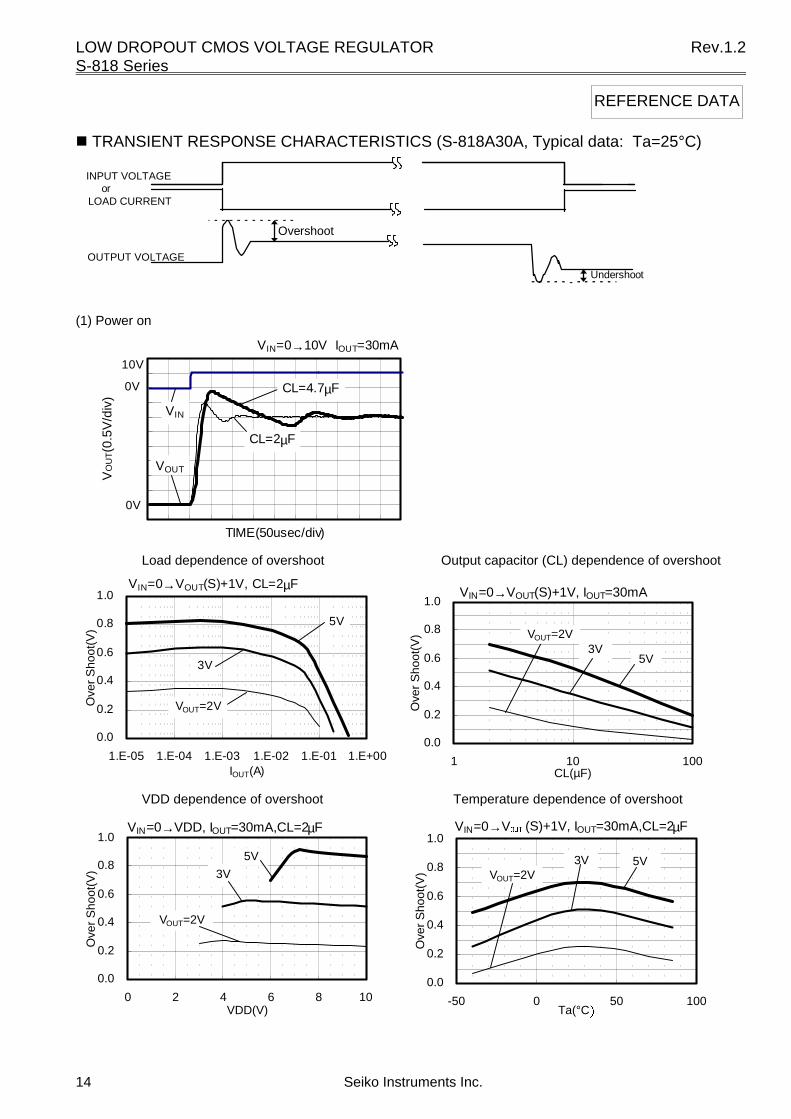
TRANSIENT RESPONSE CHARACTERISTICS (S-818A30A, Typical data: Ta=25°C)
Overshoot
INPUT VOLTAGE
OUTPUT VOLTAGE
orLOAD CURRENT
Undershoot
(1) Power on
VIN=0→10V IOUT=30mA
TIME(50usec/div)
VO
UT(0
.5V
/div
)
10V
CL=2µF
0V
0V
VIN
VOUT
CL=4.7µF
Load dependence of overshoot Output capacitor (CL) dependence of overshoot
0.0
0.2
0.4
0.6
0.8
1.0
1.E-05 1.E-04 1.E-03 1.E-02 1.E-01 1.E+00IOUT(A)
Ove
r S
hoot
(V)
5V
3V
VIN=0→VOUT(S)+1V, CL=2µF
VOUT=2V
0.0
0.2
0.4
0.6
0.8
1.0
1 10 100CL(µF)
Ove
r S
hoot
(V)
5V3V
VIN=0→VOUT(S)+1V, IOUT=30mA
VOUT=2V
VDD dependence of overshoot Temperature dependence of overshoot
0.0
0.2
0.4
0.6
0.8
1.0
0 2 4 6 8 10VDD(V)
Ove
r S
hoot
(V)
5V
VOUT=2V
3V
VIN=0→VDD, IOUT=30mA,CL=2µF
0.0
0.2
0.4
0.6
0.8
1.0
-50 0 50 100Ta(°C
Ove
r S
hoot
(V)
5V3V
VIN=0→V/54 (S)+1V, IOUT=30mA,CL=2µF
VOUT=2V
REFERENCE DATA

Rev.1.2 LOW DROPOUT CMOS VOLTAGE REGULATOR S-818 Series
Seiko Instruments Inc. 15
(2) Power on/off control
VIN=10V ON/OFF=0→10V IOUT=30mA
TIME(50usec/div)
VO
UT(0
.5V
/div
)
10V
CL=4.7µF
CL=2µF
0V
0V
VIN
VOUT
Load dependence of overshoot Output capacitor (CL) dependence of overshoot
0.0
0.2
0.4
0.6
0.8
1.0
1.E-05 1.E-04 1.E-03 1.E-02 1.E-01 1.E+00IOUT(A)
Ove
r S
hoot
(V)
5V
VOUT=2V
3V
VIN=VOUT(S)+1V , CL=2µF, ON/OFF=0→VOUT(S)+1V
0.0
0.2
0.4
0.6
0.8
1.0
1 10 100CL(uF)
Ove
r S
hoot
(V)
3V5V
VIN=VOUT(S)+1V IOUT=30mA, ON/OFF=0→VOUT(S)+1V
VOUT=2V
VDD dependence of overshoot Temperature dependence of overshoot
0.0
0.2
0.4
0.6
0.8
1.0
0 2 4 6 8 10VDD(V)
Ove
r S
hoot
(V)
5V
3V
VIN=VDD ,IOUT=30mA, CL=2µF, ON/OFF=0→VDD
VOUT=2V
0.0
0.2
0.4
0.6
0.8
1.0
-50 0 50 100Ta°C
Ove
r S
hoot
(V)
5V3V
VIN=VOUT(S)+1V ,IOUT=30mA, CL=2µF, ON/OFF=0→VOUT(S)+1V
VOUT=2V

LOW DROPOUT CMOS VOLTAGE REGULATOR Rev.1.2S-818 Series
16 Seiko Instruments Inc.
(3) Power fluctuation
VIN=4→10V IOUT=30mA
TIME(50usec/div)
VO
UT(0
.2V
/div
)
10V
CL=4.7µFCL=2µF
4V
3V
VIN
VOUT
TIME(50usec/div)
VO
UT(0
.2V
/div
)
10V
CL=4.7µF
CL=2µF
4V
3V
VIN
VOUT
VIN=10→4V IOUT=30mA
Load dependence of overshoot Output capacitor (CL) dependence of overshoot
0
0.2
0.4
0.6
1.E-05 1.E-04 1.E-03 1.E-02 1.E-01 1.E+00IOUT(A)
Ove
r S
hoot
(V)
5V
3V
VIN=VOUT(S)+1V→VOUT(S)+2V,CL=2µF
VOUT=2V
0
0.01
0.02
0.03
0.04
0.05
1 10 100CL(uF)
Ove
r S
hoot
(V)
5V
3V
VIN=VOUT(S)+1V→VOUT(S)+2V, IOUT=30mA
VOUT=2V
VDD dependence of overshoot Temperature dependence of overshoot
0
0.2
0.4
0.6
0 2 4 6 8 10VDD(V)
Ove
r S
hoot
(V)
5V
3V
VIN=VOUT(S)+1V→VDD, IOUT=30mA,CL=2µF
VOUT=2V
0
0.01
0.02
0.03
0.04
0.05
0.06
-50 0 50 100Ta°C
Ove
r S
hoot
(V)
5V
3V
VIN=VOUT(S)+1V→VOUT(S)+2V, IOUT=30mA,CL=2µF
VOUT=2V

Rev.1.2 LOW DROPOUT CMOS VOLTAGE REGULATOR S-818 Series
Seiko Instruments Inc. 17
Load dependence of undershoot Output capacitor (CL) dependence of undershoot
0
0.1
0.2
0.3
1.E-05 1.E-04 1.E-03 1.E-02 1.E-01 1.E+00
IOUT(A)
Und
er S
hoot
(V)
5V
3VVOUT=2V
VIN=VOUT(S)+2V→VOUT(S)+1V,CL=2µF
0
0.01
0.02
0.03
0.04
0.05
1 10 100CL(uF)
Und
er S
hoot
(V)
5V
3V
VIN=VOUT(S)+2V→VOUT(S)+1V ,IOUT=30mA
VOUT=2V
VDD dependence of undershoot Temperature dependence of undershoot
0
0.05
0.1
0.15
0.2
0 2 4 6 8 10VDD(V)
Und
er S
hoot
(V) 5V
3V
VIN=VDD→VOUT(S)+1V, IOUT=30mA,CL=2µF
VOUT=2V
0
0.01
0.02
0.03
0.04
0.05
0.06
-50 0 50 100Ta(°C)
Und
er S
hoot
(V)
5V
3V
VIN=VOUT(S)+2V→VOUT(S)+1V, IOUT=30mA,CL=2µF
VOUT=2V

LOW DROPOUT CMOS VOLTAGE REGULATOR Rev.1.2S-818 Series
18 Seiko Instruments Inc.
(4) Load fluctuation
IOUT=10µA→30mA VIN=4V
TIME(50µsec/div)
VO
UT(0
.2V
/div
)
30mA
CL=4.7µF
CL=2µF
10µA
3V
IOUT
VOUT
IOUT=30mA→10µA VIN=4V
TIME(20msec/div)
VO
UT(0
.1V
/div
)
30mA
CL=4.7µF
CL=2µF
10µA
3V
IOUT
VOUT
Load current dependence of load fluctuation overshoot∆IOUT shows larger load current at load currentfluctuation while smaller current is fixed to 10 µA.For example ∆IOUT=1.E-02 (A) means load currentfluctuation from 10 mA to 10 µA. Output capacitor (CL) dependence of overshoot
0.0
0.2
0.4
0.6
0.8
1.0
1.E-03 1.E-02 1.E-01 1.E+00∆IOUT(A)
Ove
r S
hoot
(V)
5V
3V
VOUT=2V
VIN=VOUT(S)+1V,CL=2µF
0
0.05
0.1
0.15
0.2
1 10 100CL(uF)
Ove
r S
hoot
(V)
5V
3V
VOUT=2V
VIN=VOUT(S)+1V ,IOUT=30mA→10µA
VDD dependence of overshoot Temperature dependence of overshoot
0
0.1
0.2
0.3
0 2 4 6 8 10VDD(V)
Ove
r S
hoot
(V)
5V
3V
VOUT=2V
VIN=VDD, IOUT=30mA→10µA ,CL=2µF
0
0.05
0.1
0.15
0.2
0.25
0.3
-50 0 50 100Ta(°C)
Ove
r S
hoot
(V)
5V
3V
VIN=VOUT(S)+1V ,IOUT=30mA→10µA,CL=2µF
VOUT=2V
Rev.1.2 LOW DROPOUT CMOS VOLTAGE REGULATOR S-818 Series
Seiko Instruments Inc. 19
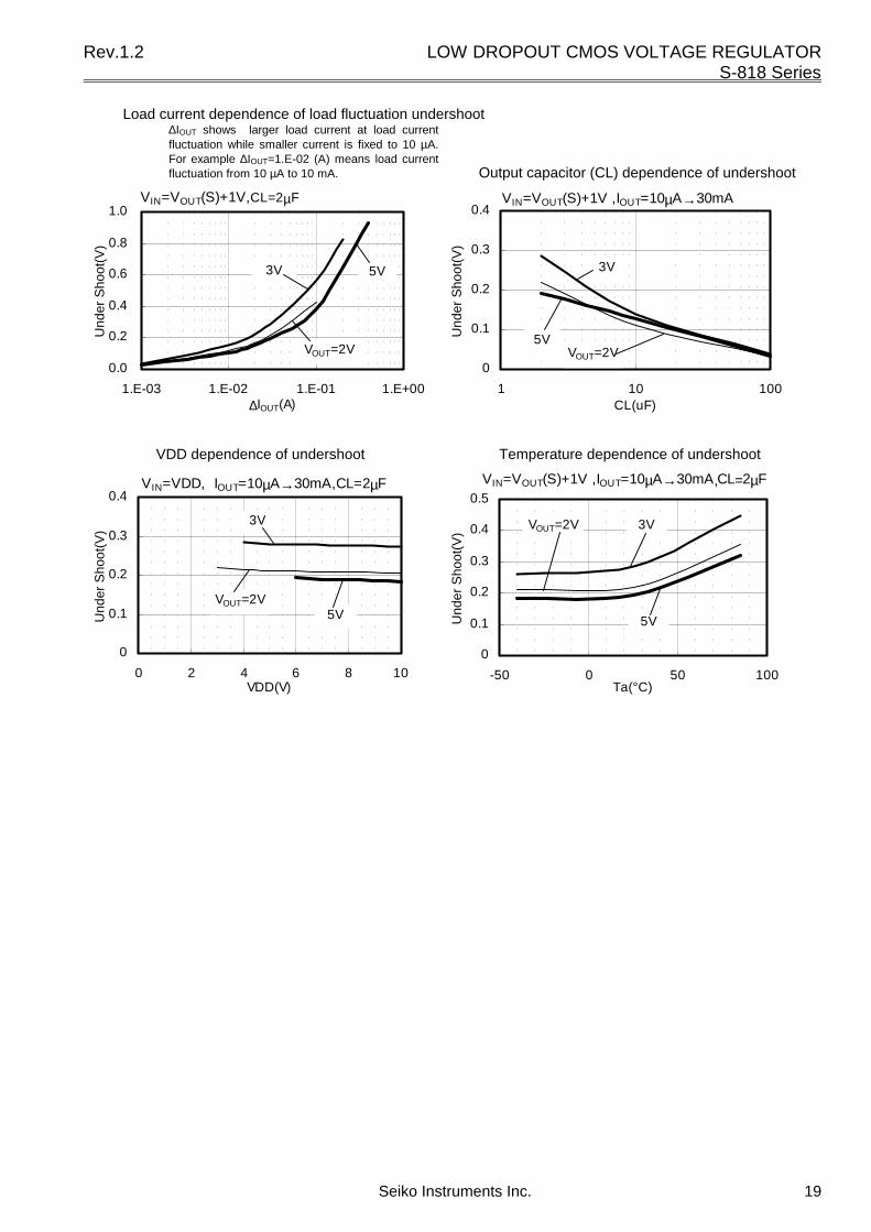
Load current dependence of load fluctuation undershoot∆IOUT shows larger load current at load currentfluctuation while smaller current is fixed to 10 µA.For example ∆IOUT=1.E-02 (A) means load currentfluctuation from 10 µA to 10 mA. Output capacitor (CL) dependence of undershoot
0.0
0.2
0.4
0.6
0.8
1.0
1.E-03 1.E-02 1.E-01 1.E+00∆IOUT(A)
Und
er S
hoot
(V)
5V3V
VOUT=2V
VIN=VOUT(S)+1V,CL=2µF
0
0.1
0.2
0.3
0.4
1 10 100CL(uF)
Und
er S
hoot
(V)
5V
3V
VIN=VOUT(S)+1V ,IOUT=10µA→30mA
VOUT=2V
VDD dependence of undershoot Temperature dependence of undershoot
0
0.1
0.2
0.3
0.4
0 2 4 6 8 10VDD(V)
Und
er S
hoot
(V)
5V
3V
VIN=VDD, IOUT=10µA→30mA,CL=2µF
VOUT=2V
0
0.1
0.2
0.3
0.4
0.5
-50 0 50 100Ta(°C)
Und
er S
hoot
(V)
5V
3V
VIN=VOUT(S)+1V ,IOUT=10µA→30mA,CL=2µF
VOUT=2V

3.25±0.15
ø1.5 +0.1 -0
ø1.0 +0.1 -0 4.0±0.1
2.0±0.050.27±0.05
1.4±0.2
Feed direction
SOT-23-5 MP005-A 991105
0.95 0.1
2.9±0.2
+0.1 -0.060.16
1.9±0.2
0.4±0.1
1 2 3
45
21±0.5
2±0.2
(60°)(60°)
φ13±0.2
12.5max.
9.0±0.3
+0.2 -0.32.81.6
1.1±0.1
0.45
1.3max
3 max.
3 max.
4.0±0.1 (10 pitches 40.0±0.2)
Taping Specifications Reel Specifications
Dimensions Unit mm
3000 pcs./reel

ø21±0.5 ø13±0.2
2±0.2
ø1.5+0.1 -0
2.0±0.1
0.3±0.05
4.0±0.1(10 pitches 40±0.2)
8.0±0.1
2.0±0.05
ø1.5+0.1 -0
4.75±0.1
Feed direction
Taping Specifications Reel Specifications
1.5±0.1 1.5±0.1
1.6±0.2
4.5±0.1
1 32
1.5±0.1
0.4±0.05
0.4±0.1
0.45±0.1
0.4±0.1 45
0.3
SOT-89-5
Dimensions
UP005-A 990531
Unit mm
3 max.
5 max.
1 reel holds 1000 ICs.

SOT-23-5
Markings990603814
SOT-89-5
4
1 3
5
31 2
45
• The information herein is subject to change without notice.
• Seiko Instruments Inc. is not responsible for any problems caused by circuits or other diagrams
described herein whose industrial properties, patents or other rights belong to third parties. The
application circuit examples explain typical applications of the products, and do not guarantee any
mass-production design.
• When the products described herein include Strategic Products (or Service) subject to regulations,
they should not be exported without authorization from the appropriate governmental authorities.
• The products described herein cannot be used as part of any device or equipment which influences
the human body, such as physical exercise equipment, medical equipment, security system, gas
equipment, vehicle or airplane, without prior written permission of Seiko Instruments Inc.