m. missous school of electrical and electronic engineering...
TRANSCRIPT

InGaAs-InAlAs Heterojunction Technologies for mm and Sub-
mm-wave applications: towards quantum limited noise
performance?.M. Missous
School of Electrical and Electronic Engineering The University of Manchester

OUTLINE
•Introduction
•InGaAs-InAlAs pHEMTs
•InGaAs-InAlAs pHEMT limitations
•Possible solutions for lowering noise
•Conclusions

There is great interest in the frequency range between 100GHz and 1THz fuelled mainly by high resolution imaging for many applications.
Sub-millimeter-wave frequencies (> 300 GHz) are now beginning to be addressed by fast transistors based on pHEMT and HBTs.
An all electronic, compact sub-millimeter-wave MMIC technology is key for the realisation of cost effective electronic Terahertz (eTHz) systems.
As low noise devices, the so-called “InP based pHEMT”are particularly attractive. However at sub-100 nm gate length , there are still a number of materials and device topology issues that need addressing.
Short channel effects and parasitics (extrinsics) are the dominant challenges to solve.
For optimising low temperature performance, new epitaxial structures may be required...
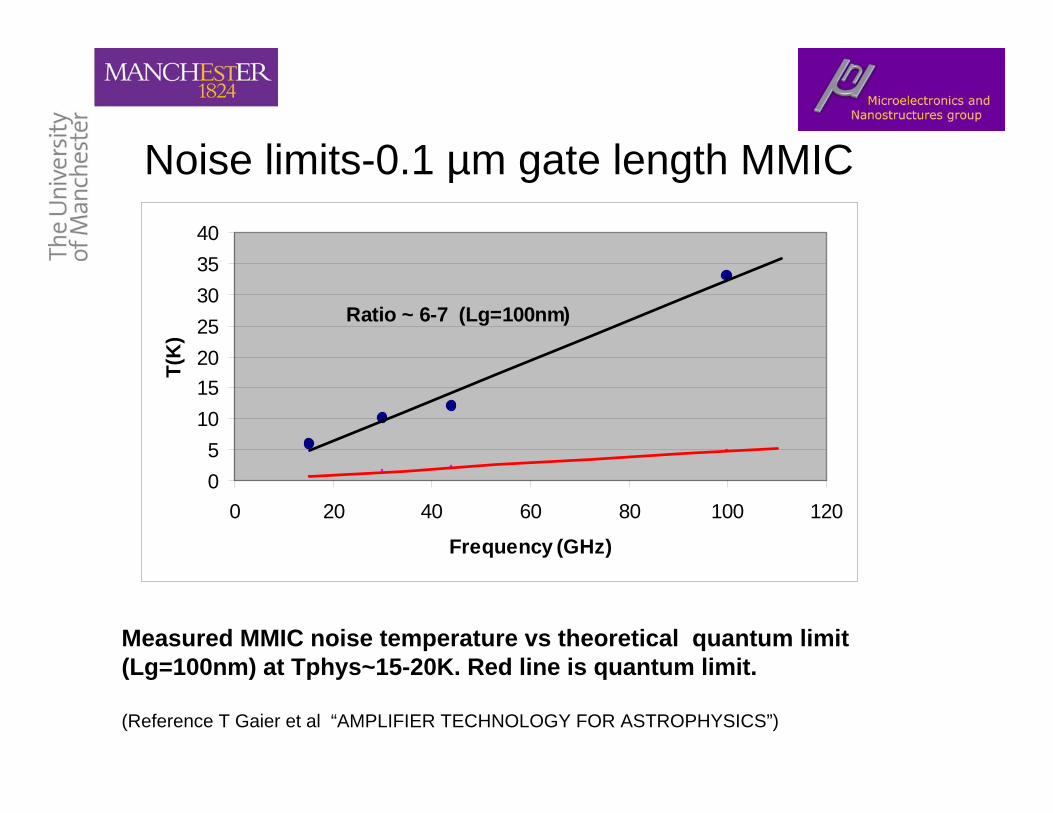
Noise limits-0.1 µm gate length MMIC
Measured MMIC noise temperature vs theoretical quantum limit (Lg=100nm) at Tphys~15-20K. Red line is quantum limit.
(Reference T Gaier et al “AMPLIFIER TECHNOLOGY FOR ASTROPHYSICS”)
Ratio ~ 6-7 (Lg=100nm)
05
10152025303540
0 20 40 60 80 100 120
Frequency (GHz)
T(K
)

Noise limits , recent progress..
Measured noise temperature vs theoretical quantum limit (Lg=100nm)at Tphys~15-20K and recent (2008) reported 35nm gate data.
0
10
20
30
40
50
60
0 20 40 60 80 100 120
Frequency (GHz)
Noi
se T
empe
ratu
re (K
) RT, Watanabe et al, single transistor IPRM 2008, Fujitsu Labs
Watanabe, Extrapolated to 4K
NGST-35nm MMIC, NRAO, unpublished
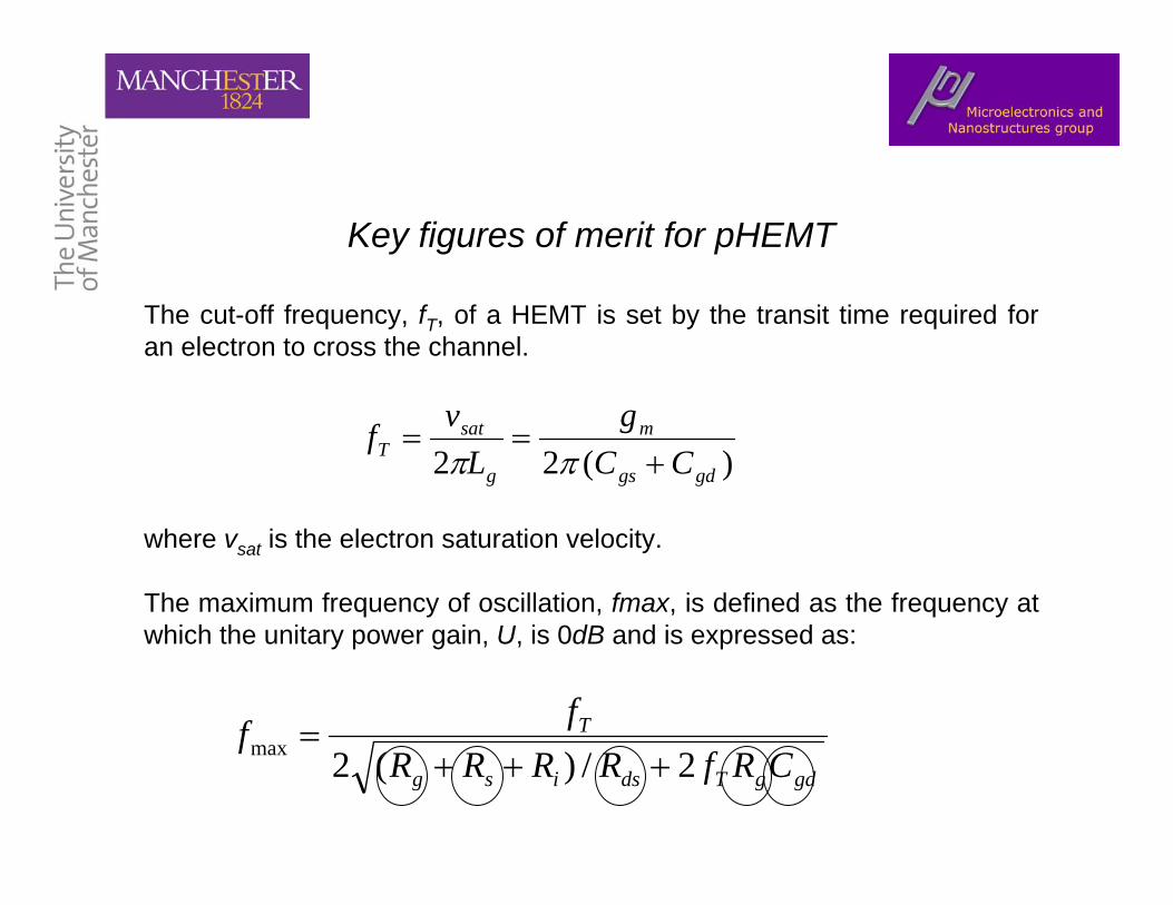
Key figures of merit for pHEMT
The cut-off frequency, fT, of a HEMT is set by the transit time required for an electron to cross the channel.
where vsat is the electron saturation velocity.
The maximum frequency of oscillation, fmax, is defined as the frequency at which the unitary power gain, U, is 0dB and is expressed as:
)(22 gdgs
m
g
satT CC
gL
vf+
==ππ
gdgTdsisg
T
CRfRRRRff
2/)(2max +++=

)1(....................2 g
sT L
vfπ
><=
fT scales with gate length BUT slower than suggested by (1).Predicted fT from (1) is ~900GHz for In.7Ga.3As channel and ~25nm.State of the art is 610 GHz at 15nm ( but Fmax only 305 GHz.) Jeong et al, 2007
TfNF /1∝
ft vs gate length
0200400600800
1000120014001600
0 50 100 150 200 250 300
gate length (nm)
ft (G
Hz) Red curve is 1/Lg
(starting at 250 nm)
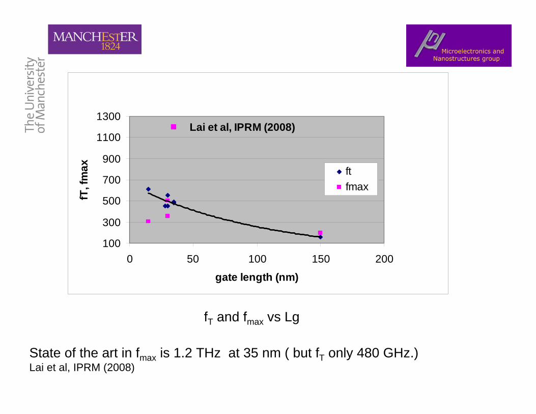
State of the art in fmax is 1.2 THz at 35 nm ( but fT only 480 GHz.) Lai et al, IPRM (2008)
fT and fmax vs Lg
Lai et al, IPRM (2008)
100
300
500
700
900
1100
1300
0 50 100 150 200
gate length (nm)
fT, f
max ft
fmax

Device OverviewDevice Overview
InP S. I. Substrate (350 InP S. I. Substrate (350 µµm)m)
InIn0.520.52AlAl0.480.48As Buffer 4500 As Buffer 4500 ÅÅ
InInxxGaGa(1(1--x)x)AsAs 12 nm12 nm
InInyyAlAl(1(1--y)y)As As 3nm 3nm
InInyyAlAl(1(1--y)y)As As 6 6 15nm15nm
InInxxGaGa(1(1--x)x)AsAsCapCap
55 10 nm10 nm
SourceSource DrainDrain
GateGate
• Lateral scaling ( Lg and dsd )
• high field effects
• Horizontal scaling
• Breakdown issues
• Leakage issues
• Aspect ratio (Lg/d) > 3
• Difficult to obtain a high ft and fmax simultaneously
• High ft requires low dsd which results in short channel effects
( drain induced barrier lowering , high output conductance)
• There is also an increase in the gate-drain capacitance Cgd and this reduces fmax of the device.
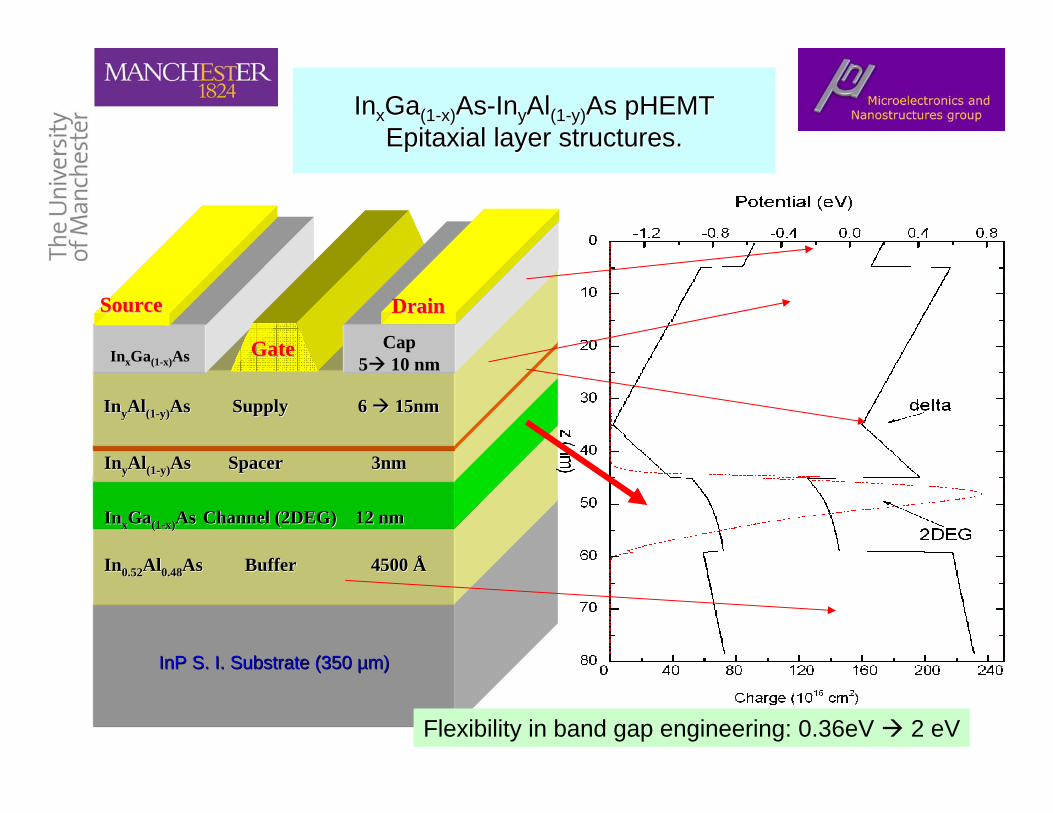
InInxxGaGa(1(1--x)x)AsAs--InInyyAlAl(1(1--y)y)As pHEMT As pHEMT Epitaxial layer structures.Epitaxial layer structures.
dLg
dsd
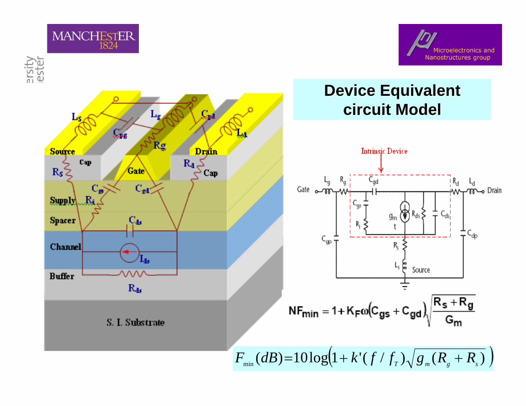
Device Equivalent Device Equivalent circuit Modelcircuit Model
( ))()/('1log10)(min sgmT RRgffkdBF ++=
InP S. I. Substrate (350 InP S. I. Substrate (350 µµm)m)
InIn0.520.52AlAl0.480.48As Buffer 4500 As Buffer 4500 ÅÅ
InInxxGaGa(1(1--x)x)AsAs Channel (2DEG) 12 nmChannel (2DEG) 12 nm
InInyyAlAl(1(1--y)y)As Spacer 3nm As Spacer 3nm
InInyyAlAl(1(1--y)y)As Supply 6 As Supply 6 15nm15nm
InInxxGaGa(1(1--x)x)AsAsCapCap
55 10 nm10 nm
SourceSource DrainDrain
GateGate
InInxxGaGa(1(1--x)x)AsAs--InInyyAlAl(1(1--y)y)As pHEMT As pHEMT Epitaxial layer structures.Epitaxial layer structures.
Flexibility in band gap engineering: 0.36eV 2 eV
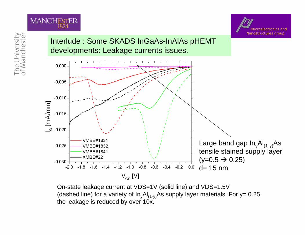
Large band gap InyAl(1-y)As tensile stained supply layer(y=0.5 0.25)d= 15 nm
On-state leakage current at VDS=1V (solid line) and VDS=1.5V (dashed line) for a variety of InyAl(1-y)As supply layer materials. For y= 0.25, the leakage is reduced by over 10x.
Interlude : Some SKADS InGaAs-InAlAs pHEMT developments: Leakage currents issues.
What about low temperature performances?
• For most applications, pHEMT are optimised for room temperature ( ~300K) performance.
• Optimise mobility and electron carrier densities
• Low temperature optimisations not necessarily the same.
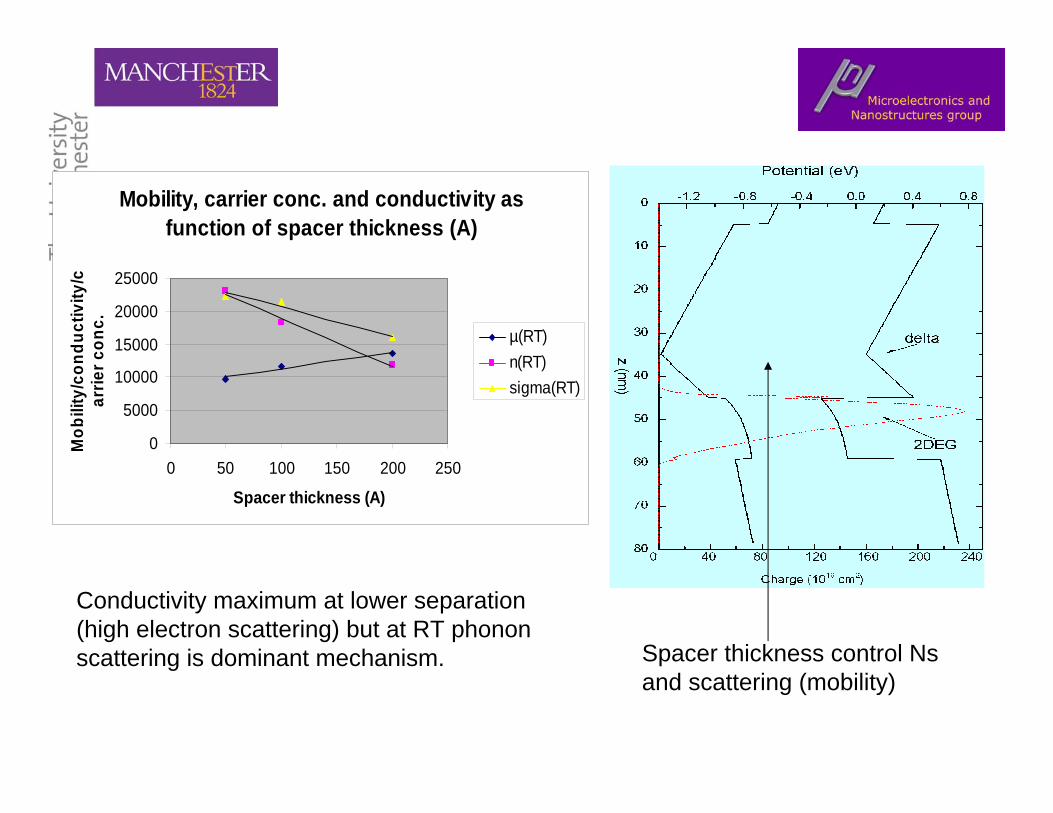
Mobility, carrier conc. and conductivity as function of spacer thickness (A)
0
5000
10000
15000
20000
25000
0 50 100 150 200 250
Spacer thickness (A)
Mob
ility
/con
duct
ivity
/car
rier c
onc.
µ(RT)n(RT)sigma(RT)
Spacer thickness control Ns and scattering (mobility)
Conductivity maximum at lower separation (high electron scattering) but at RT phonon scattering is dominant mechanism.
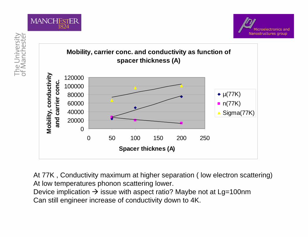
Mobility, carrier conc. and conductivity as function of spacer thickness (A)
020000400006000080000
100000120000
0 50 100 150 200 250
Spacer thicknes (A)
Mob
ility
, con
duct
ivity
an
d ca
rrie
r con
c.
µ(77K)n(77K)Sigma(77K)
At 77K , Conductivity maximum at higher separation ( low electron scattering)At low temperatures phonon scattering lower.Device implication issue with aspect ratio? Maybe not at Lg=100nm Can still engineer increase of conductivity down to 4K.
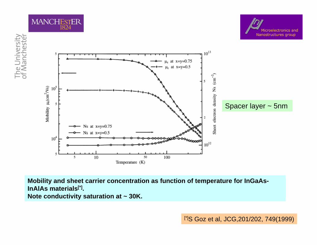
[*]S Goz et al, JCG,201/202, 749(1999)
Mobility and sheet carrier concentration as function of temperature for InGaAs-InAlAs materials[*].Note conductivity saturation at ~ 30K.
Spacer layer ~ 5nm

..and observed Noise Figure as a function of operating temperature.
NF as a function of operating T
01020304050607080
0 50 100 150 200 250 300
Physical temperature (K)
Noi
se te
mpe
ratu
re (K
)
@ 12GHz data, single transistor, 0.5µm gate length

4F1 Noise Temperature Susceptibility Test 22 Apr 2006 + 60K mean point from TV tests + RT LNA points for 4F1A1 and 4F1A2
0
20
40
60
80
100
120
140
160
180
0 50 100 150 200 250 300 350
FEM Temperature (K)
Noi
se T
empe
ratu
re (K
)
OP1 AB
OP1 BA
OP4 AA
OP4 BB
Linear (OP4 BB)
Linear (OP1 BA)
Data courtesy University of Manchester Plank team.

Data courtesy University of Manchester Plank team.
4F1 Noise Temperature Susceptibility Test 22 Apr 2006+ 60 K mean TV point, unsupressed zero
0
5
10
15
20
25
30
35
40
0 10 20 30 40 50 60 70
FEM Temperature (K)
Noi
se T
empe
ratu
re (K
)
OP1 AB
OP1 BA
OP4 AA
OP4 BB
Linear (OP4 BB)
Linear (OP1 BA)

CONCLUSIONS
• State of the at InGaAs-InAlAs pHEMT with fT and fmax of 500 GHz and ~ 1THz are beginning to emerge at gate length of ~ 30nm.
• We are still a fair way from can be achieved by at least a factor of 2 in ft.
• Reaching the quantum limit may be achieved with this material system by proper manipulation of scaling and band gap engineering of the InxGa(1-x)As-InyAl(1-y)As system.
• InxGa(1-x)As-InyAl(1-y)As is moving away from being a specialised niche technology and is road mapped for high volume , post-CMOS electronics at the 22nm node.

INTERNATIONAL TECHNOLOGY ROADMAP FOR SEMICONDUCTORS 2007 EDITION
RADIO FREQUENCY AND ANALOG/MIXED-SIGNAL TECHNOLOGIES FOR WIRELESS COMMUNICATIONS
InGaAs-InAlAs pHEMTs are on the Road Map..
14121198Associated Gain (dB)(94 GHz)
. 911.11.31.5Fmin(dB) at 94GHz
2.221.81.51.1Gm(S/mm)
500500550600500Imax(mA/mm)
1.522.534Breakdown (Volts)
500420350250200Ft (GHz)
25355070100Gate Length (nm)
201520142013201220112010200920082007Year of Production