12ghz divide by 1000 prescaler - americanradiohistory.com · 2019-11-11 · winter . 2003-q4 ....
TRANSCRIPT

A Publication for theRadio Amateur Worldwide
Especially Covering VHF,UHF and Microwaves
Volume No.35 . Winter . 2003-Q4 . £5.15
12GHz Divide By 1000 PrescalerAlexander Meier, DG6RBP


Contents
K M Publications, 63 Ringwood Road Luton, Beds, LU2 7BG, UKTelephone / Fax +44 (0)1582 581051, email : [email protected]
web : http://www.vhfcomm.co.uk
Sigurd Werner New transmitter with higher 194 - 198DL9MFV performance for 76GHzAlexander Meier 12GHz divide by 1000 prescaler 199 - 206DG6RBPDr Volker Grassmann New 144 MHz transatlantic 207DF5AI beaconGunthard Kraus Practical Project: Design and 208 - 225DG8GB construction of a high quality
100MHz bandpass filterWolfgang Schneider 1 to 65MHz DDS signal 226 - 235DJ8ES generator with a switchable
output levelEugen Berberich A new space saving 236 - 241DL8ZX omnidirectional antenna
the H O LoopCarl G. Lodström The noble art of the Rheostat 242 - 249KQ6AX & SM6MOMGunthard Kraus Funny electronic stories 250 - 251DG8GBGunthard Kraus Internet Treasure Trove 253 - 254DG8GB
This issue has a bumper number of articles. Because Christmas is coming there is aconstructional article from Carl Lodström so that everyone can build somethinguseful for the shack over the holidays. There is also a story from Gunthard Kraus tomake you think twice about buying too much junk (I mean useful equipment!).For those interested in the 12GHz prescaler, I have be warned by Eberhard Smolka ofUKW Berichte that the first batch of divider ICs that arrived was faulty. This willmean a delay if you want to purchase a kit or ready built unit. PCBs, Kits and readybuilt units will be available so if you are interested, send me an email.It only remains for me to wish you a Happy New Year and ask you not to forget torenew your subscription to VHF Communications for 2004.73s - Andy
VHF COMMUNICATIONS 4/2003
193

A simple concept for a 76GHz signaltransmitter operating as a frequencyoctupler, was described in this maga-zine recently [1]. The new W bandchip CHU3277 (from United Mono-lithic Semiconductors) is now beingtested as part of an improved andmore powerful transmitter module.Using only two MMICs, it requires a5mW input signal at 9.5GHz to gener-ate an output of 49.8mW (about17dBm) at 76GHz. The 3dB outputband covers approximately 3GHz. Op-tions for increasing the signal strengthare discussed.
1.Introduction
The octupler for 76GHz recently de-scribed [1] has proved its worth inpractice, thanks to its uncritical behav-iour. Several examples achieving an out-put of 13dBm, and in some cases consid-erably more (26mW). To enhance the76GHz signal further, a circuit has beendeveloped using two CHU2277 chipsoperated in parallel. This is no trivialmatter. Moreover, in this MMIC the RFinput has been moved through 90 degreesin relation to the RF output of the mainport [2]. The equipment works as fol-lows: The 9.5GHz signal is quadrupledusing the CHX2092a chip (38GHz) and
fed through a Wilkinson splitter to twoparallel mounted CHU2277 MMICs. Thepower levels obtained (76GHz) are fedon to two L form striplines (lengthapproximately 3mm), combined with aλ/4 Wilkinson combiner (mounted on a0.13mm quartz substrate) and finally fedto a WR12 waveguide (see Fig 1).Although it was assembled very care-fully, the results were very disappointing.The output obtained was only a mere20% higher than the level attained by astandard module of the type describedwith only one CHU2277 chip.This was clearly due to the four addi-tional substrate to substrate transitionareas. A large part of the additionalpower generated was lost at these discon-tinuities (and naturally in the Wilkinsoncombiner as well). But a more compactassembly is scarcely possible for techni-cal reasons.
2.New concept
A few weeks ago, a new 76GHz ICdeveloped by UMS was delivered,known as type CHU3277. This W bandMMIC comprises a buffer stage, fre-quency doubler and two four stage am-plifiers, which are combined into oneoutput [3]. The input signal required for
Sigurd Werner, DL9MFV
New transmitter with higherperformance for 76GHz
VHF COMMUNICATIONS 4/2003
194

38GHz is fed in at 5dBm and the outputis (typically!) 18dBm. One advantagehere (especially in relation to paralleloperation of the chip) is that the inputand output ports are mounted in oneplane (at the front of the IC in each case).The design for the following frequencyoctupler is similar to the module alreadydescribed [1]. The tried and trustedCHX2092a MMIC is again used as aquadrupler for the 9.5GHz input power,followed by the new CHU3277 chip. Theoutput signal obtained is coupled into aWR12 waveguide through a stripline.
3.Mechanical and electricalassembly
The housing, which measured 38.1mm x23mm x 15mm, was milled out of brassand then gold plated.
The quadrupler chip (CHX2092a) wasmounted on a standard aluminium nitridesubstrate (0.23mm). The W band MMIC(CHU3277) was glued onto a 0.15mmhigh platform cut out from the base ofthe cavity (depth: 4.7mm), in order tobalance out the difference in levels be-tween the ceramic substrate and the76GHz MMIC.An SMA socket at 9.5GHz was used asthe signal input. A stripline, projectinginto the WR12 waveguide on aluminiumoxide, acted as the 76GHz output. Detailsare shown in Fig 2.In contrast to the module described ear-lier (with the CHU2277 chip), thefeedthrough capacitors which lead to theDC circuits were not mounted on thehousing base but were positioned on theside walls of the cavity. This made itpossible to attach a heat sink to theunderside of the housing (Fig 3). The DClines are blocked by means of 100pFsingle layer capacitors, followed by100nF ceramic capacitors. All connec-
Fig 1: The first tramsmitter with two CHU2277 chips in parallel. TheWilkinson splitter and comnbiner can be seen clearly.
VHF COMMUNICATIONS 4/2003
195

tions between the chips and the substratewere created using 18µm gold wire andbond technology (Hybond, Model 572).
4.Results
The drive power at 9.5GHz for theCHX2092a quadrupler chip was approxi-mately 5mW. The gate voltages requiredwere set as follows:
• Gate 1 and 2, minus 0.75V• Gate 3, minus 0.15V• Drain, 3.7V (60mA)
Additional details were given in [1].The CHU3277 W band chip has aninternal power supply network, i.e. itonly requires two voltages (negative andpositive in each case). The best resultswere obtained using symmetrical volt-ages (approximately equal values). The
first effect observed, as was to be ex-pected, was proportional behaviour bythe chip over a wide range, as betweenthe current consumed and the poweremitted:At 280mA (corresponding to 4.6V ineach case), the output was 34mW, at310mA (corresponding to 5.0V in eachcase; specified as maximum value forvoltage in data sheet), the output was a42mW. (The current consumption of thenegative section of the network in allcases was between 7.5 and 10mA).The output of the MMIc was adjusted to76032MHz by the positioning of tinygold threads, and the coupling of thestripline into the waveguide was opti-mised. These miniature stubs were fixedin their positions using a UV activatedadhesive (Vitralit 5603) [4].The outputs observed at various frequen-cies with an output matched at 76GHzare shown in Fig 4. The 3dB output bandextends from 74.6 to 78.7GHz (3.1GHz).
Fig 2: The new tramsmitter using the CHU3277 chip.
VHF COMMUNICATIONS 4/2003
196

The 42mW output obtained (16.2dBm) isat the lower range of the specificationsfor the CHU3277 MMIC. The variationspecified in the data sheet (measured onthe wafer?) extends from 35mW to ap-proximately 100mW (a difference of5dB!), with a typical value of approxi-mately 60mW (18dBm ) [3]. That meansthat, in certain circumstances, it could beadvantageous to pre-select the MMICsused, for example by using specimenswith current consumption levels >300mAat the rated voltages.An alternative to this procedure, which isnot simple, could be to increase thevoltages used to more than 5V, whilesimultaneously paying attention to themaximum permissible currents. These lieat 400mA at least (the absolute limitcould even be 450mA). Thus the positivevoltage increased to 5.45V (neg. voltage5.35V), the current consumption in-creased by 330mA and the output in-creased by 46mW. A further increase inthe current, to 355mA (corresponding toapproximately 6V) yielded an output
signal of 49.8mW (just on 17dBm). Thisoutput was produced constantly for sev-eral hours in several tests, providing thatthe housing could be prevented fromheating up (e.g. by attaching a small heatsink). During short time operation (<5min) the solid brass body of the housingadequately dissipates the power loss ofapproximately 2W which occurs in themodule. Cover effects could not be de-tected, which indicates careful matchingwork.The two modules assembled to datedisplay almost identical behaviour inboth the DC and the RF performance. Iam convinced that, by using somewhathigher operating voltages (which areclearly tolerated well), together with bet-ter matching of the CHU3277 chip, the50mW output mark can soon be ex-ceeded at 76GHz.Using an experimental assembly, an at-tempt was also made to operate two ofthe CHU3277 semiconductors in paralleland to combine the power with a Wilkin-
Fig 3: Side view ofthe completedtransmitter showingthe output feed andDC supply via feedthrough capacitors.
VHF COMMUNICATIONS 4/2003
197

son combiner operating as 3λ/4 (on a0.23mm aluminium nitride substrate).However, the rather poor result demon-strates that some development work stillneeds to be carried out here (see belowalso).
5.Outlook and acknowledgements
The experiments demonstrate that highlyefficient transmitter modules can be as-sembled with only a few MMICs. Thepower level of just 50mW obtained herecould be doubled by means of a rela-tively low loss interconnection of twomodules with the same construction. In-stead of using a Wilkinson combinerwith it’s high losses, I am thinking ofarranging for power addition in thewaveguide, using a magic T, though thiswould have to be well matched. A starthas already been made on an assembly toimplement this idea. The declared objec-tive is to attain the magic level of100mW power at 76GHz.My thanks go once again to my col-leagues (Dr. Jünemann, DK7AH and Dr.Hechtfischer, DG4MGR) from Rohde &Schwarz, Munich. The ceramic sub-
strates used come from the developmentstockpile, and were modified and ad-justed by myself for the purposes de-scribed. I would like to single out Mr. W.Hohenester, who was a constant compan-ion during this project. My thanks arealso due to my friend Jochen Ehrlich(DK3CK), not only for providing me-chanical assistance but also for his tire-less constructive criticism.
6.Literature references
[1] Sigurd Werner, DL9MFV, Frequencymultiplier fro 76GHz with an integratedamplifier, VHF Communications 1/2003,pp. 35 - 41[2] Data sheet from United MonolithicSemiconductors, S.A.S. , Ref DS-CHU22770089, 29-Mar-00.[3] Data sheet from United MonolithicSemiconductors, S.A.S. , Ref. DS-CHU3277391, 01-Apr-03[4] Sigurd Werner, DL9MFV, A simpleconcept for an efficient 76GHz trans-verter, VHF Communications 2/2003, pp77 - 83.
Fig 4: Graph showing the power output from the transmitter with the 76GHzchips drawing 310mA.
VHF COMMUNICATIONS 4/2003
198

Expanding a frequency counter byadding an external precaler is a simpleand inexpensive option if you wish tomeasure higher frequencies. This newdivider module includes the 10GHzband and cuts out some tedious con-version by having a decimal divisionfactor of 1000.
1.Introduction
A high quality, universal 5GHz fre-quency divider has already been pre-sented in [1].However, the requirements set for thedivider module described below wererather different:It was to cover the 10GHz band and wasto have a decimal divider factor. Thehigh division factor of 1000 means themodule can be connected to almost anyfrequency counter. It is also a simple wayof processing the divided signal (TTLlevel) for special tasks, using a microcontroller. Thus, for example, a simple12MHz frequency counter circuit couldbe created and combined with the dividermodule to display and monitor the outputfrequency of a transmitter.
2.Resolution and accuracy
Determining the frequency of a signalsource is a fundamental measurement inhigh frequency measuring techniques,and it must, above all, be carried out veryaccurately. In this context, carrying out ameasurement is nothing but a comparisonbetween a known and an unknown value.The more accurately the known compari-son value can be represented, the moreaccurate the measurement will be.In frequency measurement, the fre-quency, f, is the reciprocal value of theperiod, t, which is a temporal value. Yettime itself is one of the most accuratelyreproducible experimental values. Thusfrequency measurement becomes one ofthe most accurately performed measure-ments.To measure a frequency, we need acounter, which counts the number ofcycles in a specific period of time (gatetime) and then standardises on a gatetime of one second. The counter isusually a digital circuit, e.g. a microcontroller, which is started and stoppedby a quartz crystal timed gate.The uncertainty, δf, of the frequencymeasurement is made up of the accuracyof the reference frequency of the timebase, δfTB, and the uncertainty of count-
Alexander Meier, DG6RBP
12GHz divide by 1000 prescaler
VHF COMMUNICATIONS 4/2003
199

ing. The uncertainty of counting amountsto ±1 cycle, since the gate time is notsynchronised with the signal frequencyto be measured. Thus, depending on theposition of the oscillations, one countingpulse more or less can be generatedduring the gate time. Depending on thelength of the gate time and the level ofthe counting frequency, this error appearsmore or less pronounced. [2]
Time base + uncertainty of countingwhere:
δf = relative uncertainty of frequencymeasurement,∆f = absolute uncertainty of frequencymeasurement,δfTB = relative uncertainty ofreference frequency (time base),tTor = time gate,f = frequency to be measured
In high frequency measurement(>100MHz), a frequency divider mustfirst be used to split these frequenciesinto smaller frequencies which the coun-ter circuit can process. This does notinfluence the part of the total errororiginating from the reference frequency.It is only the influence of the countinguncertainty (usually small) which in-creases.The resolution of a frequency counter isjust as important as the uncertainty. Thisis reciprocal to the gate time, which canbe made clearer by an example:A frequency counter has to count afrequency of 10MHz. If it counts thenumber of cycles in a gate time of 1second, it will count 10 million. It hasthus counted with a resolution of 106 Hz /106 oscillations = 1Hz.If it counted with a gate time of 100ms, itcould count only a million cycles in this
time. The resolution would thus be 106
Hz / 105 oscillations, i.e. 10Hz.It should be pointed out that frequencycounters with reciprocal counting meth-ods attain a higher resolution (usually bya factor of 10 or 100) for the same gatetime, due to their special mode of func-tioning.The resolution of a frequency counterwith a prescaler connected in series dete-riorates by the value of the divisionfactor. This is because the actual countercan only count the lower frequency thatis produced by the divider as an inputsignal.
Thus the division factor for a prescalershould be selected as low as possible.This will give the highest resolution for agiven gate time!The division factor of 1000 selected heremust now be analysed more closely:Advantages:
• Conversion on the frequency countercan be carried out very simply. Forexample, a display of 10MHzcorresponds to an input frequency of10GHz.
• The existing frequency counter needsa frequency range of only 12MHz tobe able to make full use of thefrequency divider.
• Simple further processing for microcomputer circuits based on the lowoutput frequency with TTL level.
Disadvantages:
• The resolution is reduced by a factorof 1000. So, for a measurement timeof one second, we obtain a resolutionof 1kHz, and at 100ms gate time only10kHz.
• This disadvantage, though, must beexamined still more closely with
TorTB
TorTB
tfctordivisionfaf
f
ctordivisionfat
fff
fff
⋅+=
⋅+⋅=∆= δδδ
1
ctordidvsionfaT
solutionTor
⋅= 1Re
VHF COMMUNICATIONS 4/2003
200

VHF COMMUNICATIONS 4/2003
201

regard to the combination of afrequency counter and a prescaler!There are two important points to betaken into account here:
1) Practically all frequency countersin the medium price range cancount directly only up to about100MHz. All higher frequencies(e.g. 1.3GHz input) are divideddown first, frequently by a factor of64.2) Does the uncertainty of the timebase allow for meaningfulmeasurements at high resolution?
Re. point 1:The present 12GHz frequency dividerdivides a frequency from 12GHz to12MHz. A typical frequency counter cancount these frequencies directly, with aresolution of 1000Hz at a gate time of 1second.If the 12GHz frequency divider dividedby only 10, we would have a frequencyof 1.2GHz. A typical frequency counterwould internally divide this again by 64before it could count it. The resolutionwould then be 640Hz for a gate time of 1second. So we would gain nothing.
Re. point 2:A normal frequency counter in the me-dium price range has a quartz crystal asreference, with a typical relative uncer-tainty of 10-6. If we were to measure afrequency of 10GHz (1010Hz) by directcounting, i.e. without a frequency divideror with a divider factor of 1, with a gatetime of 1 second. At the end of the daythe measurement would have an absoluteuncertainty of 1010*10-6 = 104Hz due tothe reference frequency, plus 1Hz due tothe counting uncertainty, which thusgives us 10.001kHz.If we use the frequency divider, weobtain a resolution of 1kHz for the sameinput frequency and the same gate time.At the same time, we obtain an absoluteuncertainty of 10kHz due to the referencefrequency, plus 1kHz counting uncer-tainty. This gives a total error of 11kHz.As can be seen, the error in both cases,i.e. direct counting or with a frequencydivider connected in series, exceeds theresolution with a divider. So it does notmake sense to use the divider factor toincrease the resolution.Thus the division factor of 1000 is nodisadvantage for an average frequencycounter in the medium price range!
Fig 2: Printed circuit board layout for 12GHz divide by 1000 prescaler.
VHF COMMUNICATIONS 4/2003
202

Only very high quality equipment fittedwith a precision ovened quartz crystalattains a relative reference frequencyuncertainty in the region of 10-9 to 10-11.The resolution could be meaningfullyincreased here with a smaller dividerfactor, but only if the counter can alsocount the input frequency divided by thedivider directly (i.e. without an additionalinternal prescaler)!
3.Circuit description
Fig. 1 shows the circuit diagram of thefrequency divider. The input signalpasses through the coupling capacitor,C1, to an HMC-363 12GHz divider (U1).Unfortunately divider modules oscillatewhen there is no input signal, and thisone is no exception. This behaviour is aproblem when expanding a frequencycounter. Without an input signal, theequipment registers an unstable fre-quency that is not really present. Withmany modules this can be prevented ifthe inverting input is earthed through aresistance in the kΩ range. The module
usually reacts to a reduction in resistancewith a reduction in the tendency tooscillate, but it then also has reducedsensitivity. In the present case, the ten-dency to oscillate could be suppressedusing the resistance R1, without havingtoo much of a detrimental effect on thesensitivity.The signal, divided by 8, then comes tothe 5 bit counter, U2 (HMC-394), whichis programmed with the connections A0-A4 for a division factor of 25. Here is auseful tip for anyone who is feeling alittle irritated looking at the wiring dia-gram: according to the data sheet [3], youshould select precisely the desired di-vider factor less 1.The output signal from U2 is a type ofsquare wave signal with a DC offset. Inorder to obtain a TTL signal from it,which is what the subsequent TTL di-vider needs, we use the U3 (MAX 961)rapid comparator from Maxim. It com-pares the signal from U2 with thethreshold voltage from the resistancedivider, R3 / R4, and thus generates aclean square wave signal at the outputwith an amplitude of 0V or 5Volts.In the end, it has proved necessary todevelop another synchronous counter
Fig 3: Component layout for 12GHz divide by 1000 prescaler.
VHF COMMUNICATIONS 4/2003
203

manually as a TTL divider by five. To beable to display the numbers 0 to 4, weneed 3 Bits, and thus we also need thethree JK flip-flops, U4/U5 (each74F112).The signal from the TTL divider is fed tothe output via the free AND gate used asa buffer.The operating voltage of the dividermodule (approximately 9 to 15V) is fedthrough the feedthrough capacitor, C17,and the reverse battery protection diodeD1 to the voltage regulator, U7. Thisgenerates a regulated voltage of 5V forthe divider modules. The supply voltagesfor U1 and U2 are fed through LC filtersto reduce any RF residue.
4.Assembly of circuit
The circuit diagram was used to developa board layout (Fig. 2) with the dimen-sions 71mm x 34mm This size wasselected because there were suitable tin-plate housings available. However, these
are advantageous only if the price plays asignificant role. A milled aluminiumhousings is definitely preferable. If atinplate housing is used, a suitable heatsink should be provided to cool thevoltage regulator and the divider module(especially U2). The prototype of thefrequency divider was incorporated intoa milled aluminium housing.The base material used for the throughhole plated board was 0.81mm thickRO4003C substrate from Rogers. Thisboard material has outstanding high fre-quency characteristics, but it can beworked like standard epoxy (FR4) andcan be obtained at budget prices.The 50 Ohm track width is about 1.8mm.This width should be maintained, at leastfrom the RF input to the first divider IC,U1. This track width can not always beadhered to as the RF signal moves overthe board, since the connections to thedivider ICs must be made very narrow.However, this is no great tragedy, pro-vided the tracks remain very short.The components are mounted by hand inaccordance with the component drawing(Fig. 3). Problems arise only with thedivider, U1, and the 5 bit counter, U2.
Fig 4: Completed prototype of the 12GHz divide by 1000 prescaler.
VHF COMMUNICATIONS 4/2003
204

The IC, U1, must be soldered to the eartharea on its underside (!)! This can bedone through prior tin plating, or betterusing solder paste and hot air (or a hotplane). Things become more difficultwith U2, the connections of which are, toa very large extent, on the underside ofthe chip, and where the pin distance,0.5mm (!), is extremely small.Anyone venturing to copy the dividershould therefore have a lot of experiencein soldering small SMD components.By the way, the divider, U2, runs rela-tively warm, its current consumptionbeing just on 200mA. It is cooled via itsearth area and the through plating to thealuminium housing base.Fig. 4 shows the prototype of the dividermodule.
5.Parts list
SMD capacitors:C1,C2,C5,C6 100pF 0805C3,C7,C8 1nF 0805C10,C12-C16 100nF 0805C4,C9 10µF / 35V SMD tantilum
C11 4.7µF / 3V SMD electrolyticcapacitor
C17 1nF feedthroughcapacitor, ActipassFC-102P-10A
L1,L2 10µH SIMID 1210R6,R10-R12 0Ω, 1206R2,R5,R7-R9 10kΩ, 1206R3 15kΩ, 1206R4 33kΩ, 1206R1 82kΩ, 1206D1 DL4001U1 HMC 363 S8GU2 HMC 394 LP4U3 MAX961CS8U4, U5 74F112 SMDU6 74F08, SMDU7 78051 x LP DG6RBP-0061 x Aluminium milled
housingor1 x Tinplate housing
71 x 34 x 30mm2 x SMA sockets with 4
hole flange
6.Measurement results
To test the frequency divider, a signalwith a power of 1mW (0dBm) was fed infrom a 20GHz HP 83732A signal genera-tor, and the frequency was varied be-tween 500MHz and 15GHz. The behav-iour of the divider was monitored usingfrequency counters and an oscilloscope.No functional errors could be observedhere. The output signal is shown in Fig. 5for an input frequency of 10GHz.If the divider is operated without an inputsignal, the output is either low or highlevel, depending on the counting step ofthe TTL divider. A tendency to oscillatewithout an input signal arose only whererelatively long coaxial lines were con-nected without load.
Fig 5: Output signal for 10GHz input.
VHF COMMUNICATIONS 4/2003
205

In a second test, the power was varied atconstant frequency (1GHz). In this test, itwas established that at very low powerlevels false division factors arise! Theprecise input power level at which thisbehaviour begins depends on the inputfrequency and establishes the minimumlevel required for the frequency divider.This minimum input power requirementfor the divider module is shown in Fig. 6.
7.Technical data
• Frequency range- Input min. 0.5 to 12GHz- Output 0.5 to 12MHz
• Divider factor1000
• Input level approx. 10 to +5dBm
• Output level1 5V TTL
• SWR (HF input) typ. 2...6
• Tendency to oscillate with an openinput - no²
• Connectors SMA sockets
• Operating voltage +15VDC
• Current consumption max. 350mA1 Without an input signal, there iseither a low or a high level at theoutput.2 When relatively long, open coaxialcables are connected, or in similarsituations, in certain circumstances atendency to oscillate can arise whenthere is no input signal.
8.Literature references
[1] Alexander Meier: Pre divider (:10) to5GHz, VHF Communications 1/2002, pp22 - 26[2] Thumm/Wiesbeck/Kern: High-fre-quency measuring technique, TeubnerVerlag 1997, Stuttgart[3] Data sheet HMC-394, Hittite Micro-wave Corporation, 12 Elizabeth Drive,Chelmsford MA 01824
Fig 6: Minimum input power requirement for the 12GHz divide by 1000prescaler.
VHF COMMUNICATIONS 4/2003
206

In December 2002 I received a dx reportclaiming reception of the Canadian144MHz beacon VE1SMU in Germany.The Dubus magazine finally figured outthat this beacon has been off the air formore than three years, i.e. the observedsignal did not originate from Canada butsomewhere else. Nevertheless, similarreports have existed for many years. Inthe VHF-DX email forum, the possibilityof terrestrial 144MHz transatlanticpropagation was recently discussed withpassion. European radio amateurs missthe VE1SMU beacon because there is noalternative transmitter available on theopposite side of the big pond. Now therewill be a new beacon in Canada. Pleaseread the below email information whichAndy, editor of the VHF Communica-tions magazine, and I received fromFrank, VO1HP:
“I have read with interest Dr. VolkerGrassmann’s article in your VHF Maga-zine 2-2003 edition. In that article hestates that it would be desirable to have aVHF beacon on the air from easternNewfoundland. The Marconi Radio Clubof Newfoundland (MRCN) and the Bac-calieu Amateur Radio Klub (BARK) arecurrently in the process of placing such abeacon on the air. The beacon willtransmit on 144.400MHz. The transmit-ter 250 W PA is the same one previouslyused by VE1SMU beacon. The VHF
exciter board and the CW ID board havebeen built by Joe Craig VO1NA. The 11element Cushcraft yagi, 1/2 inch feederand 35 amp power supply to run thebeacon have been donated by FrankVO1HP. The yagi and feeder were in-stalled by Boyd VO1CBS, Roy VO1XPand Joe VO1NA on August 30, 2003.The repeater site is in the middle of alarge field at a turkey farm!!....and it hasa clear view of the North Atlantic oceanthrough the mouth of Conception Bay onthe South East coast of VO1 land. It is inthe town of Carbonear at N47 45’24”W53 12’59” with the antenna at about300’ (90m) ASL and beaming at 60degrees true.The beacon VO1ZA was placed on theair on October 19th 2003 at 1330UTC on144.400Mhz by Frank VO1HP and BoydVO1CBS. Any amateur station whoclaims to have heard this beacon areasked to send reports via email to [email protected] or [email protected]. Pleasedescribe what you have heard and ifpossible the complete information beingtransmitted by the beacon.
Frank Davis, VO1HP”
Up to date information can be found onVolker’s web site http:’’www.df5ai.net
Dr Volker Grassmann, DF5AI
New 144 MHz transatlanticbeacon
VHF COMMUNICATIONS 4/2003
207

The editors of VHF Communicationsand UKW Berichte recently issued acall for readers to describe successfullyimplemented projects and thus to givea new impetus to the activities ofDIYers. Here is just such a projectthat required “intermediate develop-ment” at short notice. It did takelonger than was expected to developthe circuit and to make sure that thetargets were achieved.
1.Range of application
New projects are continually required forpractical laboratory work. Various kindsof receivers or converters can be assem-bled from a set of microwave parts, someof these will be available and some willhave to be designed and built, such aslow noise amplifiers, mixers, striplinefilters, VCOs etc.A standard commercial car radio withsynthesiser tuning and built in finalstages (2 x 12 Watts) can be used as a100MHz low frequency amplifier to re-produce FM or PSK signals, and foraudio demonstrations to large groups ofpeople.The car radio was selected because suchradios have high sensitivity and goodscreening built in as standard features,
and frequencies can also be easily ad-justed or saved through a menu drivenoperation.This bandpass filter can be connectedbetween the intermediate frequency out-put of a microwave converter and theantenna input of the radio to ensure thatin practice only signals converted to100MHz are audible even if it is theimage frequency.
2.Specifications
The following specifications were laiddown for the development of the band-pass filter:• System impedance: Z = 50Ω• Degree of filtration: n = 5• Centre frequency f0: 100MHz• 3dB bandwidth: b = 5MHz• S21 Ripple in 0.3dB
transmission range:• Transmission loss in < 10dB
pass band:• Edge steepness: at 90MHz
or 120MHz the attenuation shouldhave risen to approximately 70dBwith respect to the transmissionrange
• Filter attenuation in stop band in
Gunthard Kraus, DG8GB
Practical Project: Design andconstruction of a high quality100MHz bandpass filter
VHF COMMUNICATIONS 4/2003
208

frequency range from 0 to 1GHzmin. 70dB
• Filter type: ChebyshevNarrow Bandpass
• Mechanical: Printedcircuit board, coated with 35µmcopper on both sides, made fromRogers material R04003 with athickness of 25 MIL = 0.813mm
• Board dimensions 30 x 130mm.Incorporated into a milledaluminium housing with SMAsockets as input and output
• Distance between board and cover,13mm.
Following some test simulations, the so-called “Narrow Bandpass” was selectedas the filter type, with n = 5, which canachieve very small bandwidths. It iscreated from the familiar, standard, lowpass filter by suitable transformationwork and is characterised by the fact thatthe inductances are the same value in allthe resonant circuits.As a result of experience, L = 100nH wasselected (for with reactive impedancesexceeding 80 to 100 Ohms at 100MHzfor coils or capacitors, problems rapidlyarise with the broadband nature of thefilter properties). This only works cor-rectly if components of the highest possi-
ble quality are used.This also applies to the circuit board,hard paper or FR4 material should not beused. Only genuine microwave materialsare permissible, made from Teflon, ce-ramics or modern materials such as Rog-ers R04003 which has the combination ofexcellent mechanical and electrical char-acteristics which are not far below thoseof Teflon, even at 10GHz.This type of filter is essentially highimpedance, so it must be matched to the50Ω source or load by means of an inputor output capacitor.The circuit diagram is shown in Fig. 1.The actual filter calculations are carriedout using the free filter CAD program“fds” available from the Internet.
3.Circuit diagram of filter
Entering the design information into theinput mask of the filter program (fds), weobtain a picture like Fig. 2. You shouldtake the trouble to draw the associatedcircuit immediately, because this is actu-ally where we start to think about thepractical implementation.
Fig 1: The standard low pass filter is transformed to the narrow bandpassfilter with series capacitors and shut inductors.
VHF COMMUNICATIONS 4/2003
209

As already mentioned we will need coilsof extremely high quality and stability, sohere we use industrially manufacturedhelical components, e.g. from Neosid,with L = 100nH and a basic Q of 130.The circuit capacitors, like the input andoutput capacitors, are a combination oftwo or three SMD size 0805 standardvalues made from “NP0” material orbetter. The tiny coupling capacitors areunder 1pF and must be accurate so onlyprinted inter-digital capacitors can be
considered. Fig. 3 shows the completecircuit design.As a check, two simulations of the filtercharacteristics for the ideal case werecarried out using PUFF. Fig. 4 shows thefrequency range from 90 to 110MHz, itis easy to recognise that the requirementfor “at least 70dB filter attenuation at90MHz” is adequately met. Fig. 5 showsthe permissible Chebyshev ripple of0.3dB in the pass band and confirms theefficiency of the free filter program used.
Fig 2: The results produced by the filter design program "fds".
Fig 3: Thecompleted circuitshowing thecapacitors thatmust beconstructed asinter-digitaldevices.
VHF COMMUNICATIONS 4/2003
210

4.Realisation of the inter-digitalcoupling capacitors
The values required for the couplingcapacitors are very low and lie between0.5 and 0.9pF, but must be producedwith a high degree of precision. For thisreason, discrete solutions are excluded,and we are left with a “printed format”.
The design of such capacitors, usingnomograms, has already been describedin VHF Communications articles. [1] [2].However, when the first attempts weremade to assemble the printed circuit onthe board, it became clear that the diver-gences of 10% to 15% between theoryand practise arising using these proce-dures can not be tolerated and anothersolution is required. Fortunately, the freestudent version of APLAC allows for thesimulation of an individual capacitor ofthis type with really high precision, al-though it then refuses to examine thecomplete filter circuit saying “Memoryrestricted in this version....”.We therefore propose the following path:• The two inter-digital capacitors
required (0.675pF and 0.842pF) areindividually developed andoptimised one after the other. Inaddition, an S parameter file isgenerated for each capacitor that canbe entered into the PUFF simulation.
• The complete filter circuit is firstsimulated using PUFF and then
Fig 4: PUFF simulation showing adequate attenuation at 90 and 120MHz.
Fig 5: Chebyshev ripple in the passband.
VHF COMMUNICATIONS 4/2003
211

manually optimised (the inter-digitalcapacitors not only affect couplingbut also add extra inherentcapacitance to the circuit capacitors,the latter must be correspondinglyreduced).
• Only now is the coil Q taken fromthe data sheet also inserted into thecircuit as a loss resistance for anyinductance and thus simulates thetransmission curve to be expectedfrom the structure of the printedcircuit board.
We began with the design of the smallcapacitor of 0.675pF. The first step,according to the start of the APLACprogram, is to open a new file and thenright click on the empty screen. Under“Basics”, we find the components “Port”and “Ground”, each one is needed twice(but in the student version they have tobe called up individually one after theother). The inter-digital capacitor can beinserted by right clicking on mouse /microwave / microstrip / Micap. Follow-ing positioning of these five components,double click on the left hand mousebutton on a free space, which allows aroll of wire to come out of the cursor andthe circuit can be wired up (see also theAPLAC presentation in [3]).The S parameter file for the simulatedcapacitor is not generated until you have
clicked on the output port and, under“Attributes”, entered the lineSTORE C0675.s2p GHZ MA
The two system resistance ports havealready been automatically selected at50Ω, as the entry “50” is automaticallyposted. However, to make things clearer,you should always make all attributesvisible. Now the crucial question arises:how are the technical details of an inter-digital capacitor programmed?Fig. 6 can help us here, since it originatesfrom the corresponding manual (RFComponents / Microstrip Parts / Micap)and tells us what APLAC needs forcorrect simulation, where:• W = Finger width• L = Finger length• N = Number of fingers• S = Finger interval• Ge = Gap at end• WT = Width of connecting line for
individual fingers on each side,which is indicated as TransmissionLine.
• WF = Width of microstrip supplyline leading to capacitor connections
0.25mm was selected for the fingerwidths and the various intervals. Firstly,this can be controlled satisfactorily bythe board manufacturer, and secondly
Fig 6: APLACmodel for aninter-digitalcapacitor showingthe relevantdimensions.
VHF COMMUNICATIONS 4/2003
212

this value is not so high that it brings thedesired coupling capacity down too far.The selection of six fingers was based onthe older designs already mentioned [1],[2], and the start value for the fingerlengths was likewise taken from themand subsequently optimised. These val-ues must now be correctly transferredinto the attribute field of the capacitor(after double clicking on the symbol) InFig. 7 all the moves discussed can beseen. Just make sure that an additionalvariable, “N1”, has been introduced forthe number N, and that a new variable,“Len”, has likewise been introduced forthe finger length. This is not absolutelynecessary, but it makes things clearer foroutputting the calculated values later.Moreover, it is now high time this projectwas saved under a suitable name.In addition, the “Object Box List” wasalso mixed in. It keeps a record of thenecessary simulation files and can alwaysbe called up onto the screen using “Pres-entation / Show Object Box List”. Theentry “Isweep” (which can not be usedhere!) is deleted.Five new files have to be added toexisting “Circuit File”. These are de-scribed in detail below. Please note thatthe sequence of the following files in theObject Box List must be adhered to...
The “Declare” fileIn this file, all “Initialised APLAC vari-ables” (IAPLAC- VAR) required laterare declared. They must always have astart value of some sort. In the simplestcase, just enter a “1”. We then have:
IAPLACVAR Leff=1.0IAPLACVAR Cg=1.0IAPLACVAR Cm=1.0IAPLACVAR Cgtot=1.0IAPLACVAR Cmtot=1.0IAPLACVAR Len=7.30mmIAPLACVAR N1=6
Comments:Leff - represents the actual effectivefinger length, calculated by the pro-gram.Cg - expresses the grounded capacitanceper unit length, i.e. the additional rela-tive inherent capacitance per unit lengtharising. It will detune the resonant cir-cuit to the left and right of the capacitor.Cm - corresponds to the coupling capac-ity desired, though once again expressedper unit length.Cgtot - is the actual effective inherentcapacitance for each individual capaci-tor connection, by which the associatedcapacitor must be reduced. It is calcu-lated as the product of Cg and theeffective length, Leff.
Fig 7: Thecompletedsimulation of aninter-digitalcapacitor usingAPLAC.
VHF COMMUNICATIONS 4/2003
213

Cmtot - is the true objective: the actualcoupling capacitance, calculated as theproduct of Cm and LeffLen represents the finger length verifi-able in the layoutN1 - is the number of fingers used.The “Msub” fileAll the data concerning the board mate-rial (Rogers R04003) and the circuitboard are contained in this file. Thefollowing entries are needed:ER=3.38H=0.813mmT=0.035mmRHO=0.75RGH=2umTAND=0.0005COVER=13mmLEVEL=2
The following details are included, inthis order:Relative permittivity: 3.38Board thickness: 0.813 mmCopper coating: 35 µmSpecific resistance of copper in com-parison with gold: 0.75Surface roughness: 2µmBoard material dielectric loss factor:0.005 where f = 100MHzDistance between board and cover: 13mmLEVEL = 2 means simulation must beextremely precise, regardless of theamount of calculationThe “Circuit” fileIt is automatically set up when the wiringdiagram is drawn and no additional en-
tries are required.The “Sweep” fileThis is not only used to generate the Sparameter file for the desired capacitor,but also allows S11 and S21 to berepresented in the frequency range from1kHz to 3GHz. A start value of 1kHz isused because AppCad 3.0 gives an errormessage if the frequency in an S param-eter file begins with zero.The “Sweep” file required is shown inTable 1.Significance of individual lines of“Sweep” file:• 1st line: Designation of simulation
project, included in desired printouts• 2nd line: Simulate 1001 points in
frequency range from 1kHz to 3GHzand divide this range up linearly.
• 3rd line: Provide diagram foroutputting results with vertical axisdivided up from 40dB to zero dB.
• 4th line: It must always be empty,must NEVER be forgotten andseparates the simulation section fromthe display section
• 5th line : Display magnitude cycle ofS11 in zero window
• 6th line: Display magnitude cycle ofS21 in same window.
The “Text” fileThis is used in calculation and savedseparately as a public declared variable,and subsequently determines the precisecapacitor data (see entries and commentsin “Declare” file):Call Leff=Ref(Micap1,L)
"Interdigital Capacitor 0.675pF"LOOP 1001 FREQ LIN 0.000001GHz 3GHzWINDOW=0 Y "" "dB" -40 0SHOW W=0 Y MagdB(S(1,1))
+Y MagdB(S(2,1))
Table 1: Contents of Sweep file.
VHF COMMUNICATIONS 4/2003
214

Call Cg=Ref(Micap1,C1)Call Cm=Ref(Micap1,C)Call Cgtot=Cg*LeffCall Cmtot=Cm*LeffThe”Print” fileIt provides for the outputting of thecalculated parallel and coupling capaci-ties on a page of their own. To makethings clearer, “LF” stands for line feed.And "S" identifies a string. This is theassociated explanatory text (Table 2).If this work is correctly done (and thenew files are listed in the specifiedorder), the simulation can be started
using <Control + S>.After the necessary calculation time,something appears on the screen. Butonly the printout is important (Fig. 8),whilst the representation of the S param-eter is more for information. To makethings clearer, it should be explained thatthe calculated values are always output inthe basic units. The entries must there-fore be indicated in the following way:• Number of fingers = 6• Finger length = 7.30mm• Total effective inherent capacitance
on each side = 535.489 Femtofarads= 0.535pF
Table 2: Contents of Print file.
LF LFS "Calculation of an Interdigital Capacitor of 0.675pf"LF LFS "Number of Fingers = "REAL N1LFS "Length of a finger = "REAL LenLFS "Total grounded capacitance on every side = "REAL CgtotLFS "Total coupling capacitance = "REAL CmtotLF
Fig 8: TheAPLAC printoutfor the 0.675pFinter-digitalcapacitor.
VHF COMMUNICATIONS 4/2003
215

• Total coupling capacitance = 675.01Femtofarads = 0.675pF.
The 0.842pF capacitor is also calculatedin this way. In the “Declare” file, thenumber of fingers is altered to N1 = 8and the finger length is changed to Len =6.44mm. And dont forget to double clickon the output port on the screen andchange the designation of the S param-eter file in “C0842.s2p”. Now save,under a new name, and then check thesequence of files, carry out a simulationand incorporate the result:• Number of fingers = 8• Finger length = 6.44mm• Total effective inherent capacitance
on each side = 601.940 Femtofarad= 0.602pF
• Total coupling capacitance =842.387 Femtofarad = 0.842pF.
So APLAC has completed its task andcan be shut down again.
5.Preparation of circuit with thehelp of PUFF
Preliminary note on PUFF:To simplify working with PUFF, wecreate a new folder for a new project andunzip or copy PUFF2.1 into it. Thisfolder is then given the name of thecorresponding development and an Iconwith the same name on the Windowsscreen. You should only work with thebetter Protected Mode version of PUFFand should therefore set up a path to thepuffp.exe file! Right click on your PUFFicon and select the properties. Select thememory tab and use the settings shownas per [4] and [5]. Activate “Auto”under the “Conventional memory” head-ing in both windows. Under EMS, XMSand DPMI the entry required is 4096Kilobyte. You can now experiment withPUFF without problems. Once develop-ment work has been completed, only theresults data are saved, and then theoperations folder is deleted again.
Table 3: Setup file for PUFF showing important parameters in bold.
\board .puf file for PUFF, version 2.1dd 0 display: 0 VGA or PUFF chooses, 1 EGAo 1 artwork output format: 0 dot-matrix, 1 Laser Jet, 2 HPGL filet 0 type: 0 for microstrip, 1 for stripline, 2 for Manhattenzd 50.000 Ohms normalizing impedance. 0<zdfd 0.100GHz design frequency. 0<fder 3.380 dielectric constant. er>0h 0.813mm dielectric thickness. h>0)s 200.000mm circuit-board side length. s>0c 160.000mm connector separation. c>=0r 0.010mm circuit resolution, r>0, use Um for micrometersa 0.000mm artwork width correction.mt 0.035mm metal thickness, use Um for micrometers.sr 5.000Um metal surface roughness, use Um for micrometers.lt 5E-0004 [dielectric loss tangent.
VHF COMMUNICATIONS 4/2003
216

After that preliminary note, we can getstarted. Open Windows Explorer andcopy the two S parameter files generatedby ACLAP (C0675.s2p and C0842.s2p)into this new PUFF folder. Then use thetext editor to open the setup.puf file, toenter the correct material and circuitboard data.Table 3 lists the data from the file for theRogers R04003 circuit board used (theimportant points are in bold type!).Once this is complete, start PUFF andenter one component after another in listF3. However, the entire circuit must bemodified compared with Fig. 3 and Fig.4, at the following points:Instead of the discrete coupling capaci-tors with 0.675pF or 0.842pF, the two Sparameter files generated by APLAC,C0675.s2p and C0842.s2p, are now used.This happens in F3 with the two lines:device C0675.s2pdevice C0842.s2p
In addition, in all five resonant circuitsthe circuit capacitors must be reduced by
the additional inherent capacitances in-troduced by the adjacent inter-digitalstructures. This produces the followingchanges:• First and fifth circuits:
Ccircuit = 19.540pF 0.602pF =18.938pF
• Second and fourth circuit:Ccircuit = 23.810pF 0.602pF0.535pF = 22.637pF
• Middle circuit:Ccircuit = 23.980pF 0.535pF0.535pF = 22.91pF
If we now repeat the simulation as perFig. 4 with this circuit changed in thisway, the result seems rather a long wayfrom the desired ideal (Fig. 9). Fortu-nately, the solution is relatively simple,since the reason for this situation shouldbe sought in the (simple!) relationshipsbetween the frequencies and the inter-digital capacitance values! So you keepmaking careful corrections to the valuesof the resonant circuit capacitors untilyou have achieved the best compromise.Fig. 10 shows this objective and the
Fig 9: PUFF simulation using inter-digital capacitors showing results that arenot ideal.
VHF COMMUNICATIONS 4/2003
217

capacitor modifications required for it.Things don't get interesting until youbring the actual coil losses present intothe simulation. With the Neosid helicalfilters used, the data sheet specifies abasic Q of Q = 130 for the frequency f =100MHz. However, if you rotate the coreinward during adjustmets in order toreduce the inductance, then this quality isreduced! We are actually dealing withbrass cores, into which eddy currents areinduced via the coils magnetic field, thusreducing the inductance. But this isequivalent to an increase in losses and itis more advantageous to work with aquality of only Q = 100. If we considerthese losses as a series resistor for eachcoil, then we must set 0.63Ω on eachside. Fig. 11 shows the effects of theselosses. They cause the transmission lossto increase to approximately 7.3dB,whilst the stop band remains practicallyunchanged.It becomes interesting later on to com-pare the measured results with this pre-diction, for so far, very optimistically, wehave assumed that all circuit capacitors
are ideal and loss free and we musttherefore undoubtedly count on anotherslight deterioration.
6.Practical construction of thebandpass filter
The board dimensions are defined by thehome made milled aluminium housing,with a screwed on screening cover, usedby the author. These dimensions are usedfor all microwave circuits and, ongrounds of rationalisation, they nowcome in only the two board sizes, 30mmx 50mm and 30mm x 130mm. The fourfixing screws are then arranged in a grid,24mm x 44mm or 24mm x 124mm.If you take a closer look at the bandpassfilter circuit board (Fig. 12), you willvery quickly recognise the principleused, which is a tried and trusted one formicrowave circuits:
Fig 10: PUFF simulation using inter-digital capacitors showing results afteradjusting the capacitor values.
VHF COMMUNICATIONS 4/2003
218

The underside of the circuit board is acontinuous earthing area. The two SMDcoupling capacitors are inserted at theinput and output in the continuous 50Ωmicrostrip line, which has a width of1.83mm, on the top face. In addition, thisline is interrupted by the four inter-digitalcapacitors required. The five insulatedearthing areas, with numerous feedthrough links, are designed for the fiveresonant circuits. Do not use any otherearthing areas for frequencies from100MHz upwards, since these throughhole plated islands ensure low inherentinstability and satisfactory broadband be-haviour!
The helical filters do pose one smallproblem due to their overall height,which with the connecting feet are ap-proximately 15mm, and thus exceeds theclearance height of 13mm between thecircuit board and the cover. This problemis solved by flush mounting with thesilver plated housing soldered directly tothe associated earth islands.The circuit diagram and the componentsrequired can be seen in Fig. 13, whilstFig. 14 shows the final structure.If you add up the capacitances in eachindividual circuit and compare them withthe values calculated above and then add
Fig 11: PUFF simulation showing the effect of losses.
Fig 12: Printed circuit board layout for the 100MHz bandpass filter.
VHF COMMUNICATIONS 4/2003
219

in the capacitance of the continuousstripline (the circuit board data selectedgives an inherent capacitance of approxi-mately 0/5pF for a line length of 5mm),you come to the conclusion that thesoldered component values are too high!.This is true, but when the core is fullyrotated out the helical filters have amaximum inductance of 100nH, whichcan be reduced right down to 93nH whenthe core is rotated in (see above!). Thus itis preferable to add a little extra to thecapacitance and tune the filter correctly.The following measurements indicatethat these observations are correct.
One problem remains: after the filter isbuilt how do you get at the inductorcores? One solution would be suitablypositioned tapped holes in the housing,which are closed using grub screws. Buta second method works better on thisfilter, with minimal stray fields. Use twosmall copper plates as carriers for the twoSMA sockets at the input and output. Thecentral conductors of the sockets aresoldered to the associated microstriplines and the plate squares are simplyscrewed to the circuit board. Fig. 15shows this arrangement. Now the circuitboard can be connected to the networkanalyser, measured and correctly tuned.
Fig 13: Final circuit diagram for the 100MHz bandpass filter.
Fig 14: The completed 100MHz bandpass filter in its aluminium housing.
VHF COMMUNICATIONS 4/2003
220

A subsequent measurement check fol-lowing incorporation into the screeninghousing, with the cover screwed on,shows that the transmission curve is notnoticeably altered as a result.Incidentally: this method is also ex-tremely useful for rapid, basic functionaltesting of all microwave circuits in therange up to 10GHz. When equipment isin a housing the first thing you areusually struggling against is the fact thatthe layout acts as a waveguide or a cavityresonator, with its natural resonances andother effects. It usually needs a bit ofeffort, e. g. using conducting foamedmaterial glued to the inside of the coveror additional dividing walls, to get con-
trol of these “bad habits”.
7.Measurement results
Fig. 16 shows the transmission curve inthe frequency range from 90 to 110MHz,so that we can make a direct comparisonwith the simulation as per Fig. 11. Natu-rally, there are difficulties with the rise inthe transmission loss to 10dB (as wefeared). If we carry out a few morespecimen simulations with varying lossresistance values, then this gives us aseries resistance of 0.88Ω for each coil,
Fig 15: The bandpass filter with SMA connectors fitted to copper plates.
Fig 16:Transmissioncurve from 90 to120MHz.
VHF COMMUNICATIONS 4/2003
221

or Q = 72. But since not only the coilsbut also the capacitors play a part inthese losses, it would be rewarding to doanother experiment here using very ex-pensive but high quality microwave ce-ramic capacitors (as incorporated used inthe Satellite LNBs).Finally, Fig. 17 shows the stop band inthe range from 100kHz to 1GHz. Inprinciple, no unpleasant surprises shouldbe expected here as, through the use ofseveral SMD capacitors in each resonantcircuit, the inherent resonance is pushedsufficiently far upwards. To recap: theinherent inductance of these capacitorsdoes not depend on the capacitance valuebut on the size of the housing, and for“0805” is about 0.5nH. If we use severalcapacitors in parallel the inductances isin parallel and there is a correspondingfall in the total inductance. So it is onlyabove this inherent resonance that thefilter attenuation collapses, because theresonant circuit no longer displays ca-pacitive behaviour, being replaced byinductances. And unfortunately their re-active impedances then diminish as thefrequency rises.The reduction in the filter attenuation as
the frequency rises can be prevented.Since we are dealing with a direct cou-pling of the output to the input the effectsof these capacitors own inherent induct-ance, which we have just been discuss-ing, also have a role to play here, wemust use three capacitors in each reso-nant circuit, instead of just two.One other comment: as a precaution, theinside of the cover was laminated with aconducting foamed material 2mm thick,in order to suppress the expected housingresonances in the GHz range. However,the effect of all these measures for therange exceeding 1GHz was not investi-gated further.
8.Summary and outlook
The combination of modern design andsimulation software, including undesir-able “parasitics”, together with a correctcircuit board layout and correct housingconstruction, means that nowadays evena DIYer of limited means can assemblehigh quality circuits with precisely pre-
Fig 17: The stopband from100KHz to 1GHz.
VHF COMMUNICATIONS 4/2003
222

dictable characteristics. Converting toother frequencies is not a problem either,a pocket calculator and version 2.1 ofPUFF are all you need!In conclusion, I'd like to make a wishcome true for a radio ham friend of mine:During a technical discussion on theproblems arising in relation to the devel-opment of the bandpass filter, he said:“Now, do something aimed directly atradio amateurs. I could make good use ofa filter like that if I could use yourconverter idea, but with a 2m receiverinstead of the car radio”.He's right, and so Fig. 18 shows just sucha design. For this project, the circuitinductance has been reduced to 72nH(for the next smallest filter obtainablecan be altered only between 76nH and67nH) and the band width has beenincreased to 6MHz due to the highermean frequency. The simulation in therange of 120 to 160MHz is shown in Fig.19, where the work was carried out withQ = 100 (this shows the enormous valuesfor the stop band at 120 or 160MHz!).Complete development requires a little
more work because the microstrip line inthe centre of the board shows up parallelcapacitances for each resonant circuits.True, these are only percentage changes,but this influence unfortunately doesslowly make itself felt.A series of such line sections with vari-ous lengths can be listed in PUFF list F3and they can be introduced between theindividual filter components in accord-ance with the board layout. Then, ofcourse, comes the laborious precisionwork to correct the circuit capacitors.Due to the higher operating frequency,the direct capacitive coupling betweenthe input and output sockets within thehousing can now have a greater effect onthe filter attenuation and can make itworse. So presumably dividing walls arerequired and it looks as if this couldmean a new, independent project.
Fig 18: A design for a 145MHz filter using "fds".
VHF COMMUNICATIONS 4/2003
223

9.A disadvantage whichunfortunately could not beavoided
Everything is working excellently, thefilter is doing its duty, the articles writtenand now it has to be sent off. What isthere left to do? Well, something doescome creeping up now from an unex-pected quarter. In this case from Finland- the CD with the newest test version7.80 of APLAC turned up on my desk.So you run the update and, just forinterest, test the improvements, using thenew version on existing completedprojects. And what does this lead to?True, you can certainly calculate theinter-digital capacitor again, with its di-mensions and fractional capacities, butgenerating the S parameter file (and thusthe sweep) is barred, the reason givenbeing “Memory restricted in this ver-sion”. Following several emails andsome overheating among the specialist
brains working things out in Helsinki,this is the situation:• The two tasks (i.e. S parameter
sweep AND capacitor calculation)can function together only if you useversion 7.51, which is indeed whatthe author has been using up to now.
• With the newer versions, only thecapacitor calculations can be carriedout since, due to the recentlyimproved model, the simulation costfor sweeps has increased, and hastherefore exceeded the limits of thestudent version.
• APLAC is rather embarrassed, andin such circumstances may well wishthey'd been a bit less nit-picking inissuing cheap-rate “University andEducation Licenses”. So they arebeing very generous about issuingfree 45 day test complete versions(and you can apply more thanonce....). But please contact APLACdirect with your queries!
The author can also suggest anothersolution, which is to carry on using the
Fig 19: PUFF simulation of a 2m bandpass filter from 120 to 160MHz.
VHF COMMUNICATIONS 4/2003
224

previous version 7.51. His email addressis: [email protected]
10.Literature references
[1] Puff beginners project: Low-noiseamplifier for the 137MHz NOAAweather satellite range or for the145MHz 2m amateur radio band. Part 3,Section 12.2.: Building an inter-digitalcapacitor by Gunthard Kraus. UKWBerichte 3/1999, Page 170 (This articledid not appear in VHF Communicationsbut can be translated if there is sufficientdemand - Andy)[2] Design and building of microwave
circuit .Part 10: Development of a 2GHzoscillator. Section 13.7.: Dimensioningof an inter-digital capacitor by GunthardKraus. UKW Bericte 2/1999, Page 117(This article did not appear in VHFCommunications but can be translated ifthere is sufficient demand - Andy)[3] An Interesting Program APLAC byGunthard Kraus. VHF Communications2/2003, pp 90 - 105.[4] Problem with running Puff on Win-dow 98, Windows ME and Windows XP,and how to eliminate them by GunthardKraus. VHF Communications 4/2002, pp229 - 231.[5] Lets try again with PUFF byGunthard Kraus. VHF Communications3/2003, pp 170 - 180.
VHF COMMUNICATIONS 4/2003
225

One extremely important aid for theactive radio amateur is a signal gen-erator. Whether you need a test signalto check the short wave receiver, oryou want to re-calibrate the S meter oryou'd like to measure the quartz filteryou've assembled, the areas of applica-tion are numerous. Since a large partof DIY activities is involved with theshort wave area, the signal generatordescribed below is designed for therange of 1 to 65MHz. The signal levelcan be adjusted in 1dB steps between-117dBm and +10dBm and the fre-quency can be selected to 1Hz resolu-tion.
1.General
In recent years, new DDS (Direct DigitalSynthesiser) components have been con-tinuously coming onto the market. Mod-ern DDS components, with their simpleexternal wiring supply sinusoidal outputsignals going far up into the VHF range.One possible area of application for thiskind of frequency generator is, for exam-ple, as a signal generator. For generalcontrol of the DDS component, it makessense to use a micro controller, whichmakes various control options possible,together with the displays showing thefrequency and other parameters.
The system determines that the outputsignal shall be filtered through a highquality low pass filter. In addition to thedesired frequency (the fundamental), aDDS also generates alias products suchas the clock frequency + the fundamentaland clock frequency fundamental. Alsothe clock frequency multiplied by two,three, etc. This also gives an endlessnumber of mixed products. These can beremoved using a fixed low pass filter at30 to 40 % of the clock frequency.You can find additional details aboutDDS ICs in [1] and [2].The DDS signal generator with switch-able output level, consists of the twofunction blocks:• DDS with control and display• Controlled amplifier with adjustable
attenuator.The controlled amplifier followed by anadjustable attenuator gives an output sig-nal level range of -117dBm to +10dBm.The usable frequency range is 1 to65MHz. All adjustments are carried outby the micro controller.
2.Description of circuit
The core of the circuit is the AD9851
Wolfgang Schneider, DJ8ES
1 to 65MHz DDS signalgenerator with a switchableoutput level
VHF COMMUNICATIONS 4/2003
226
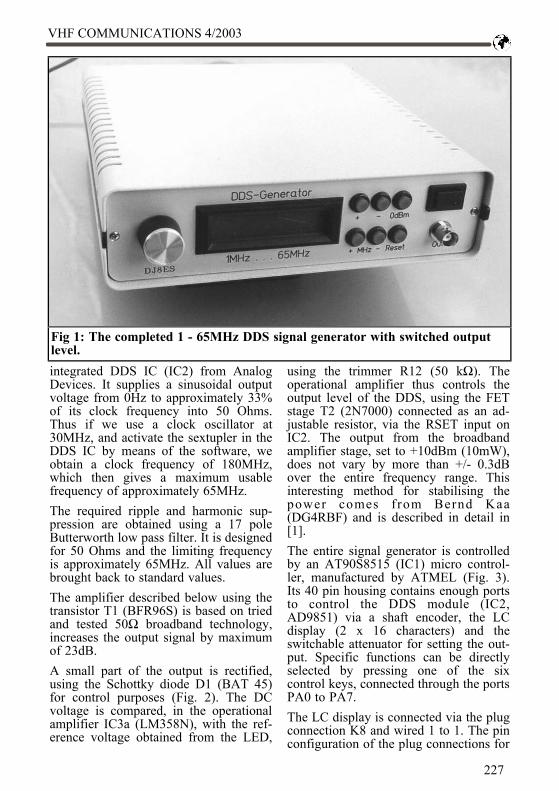
integrated DDS IC (IC2) from AnalogDevices. It supplies a sinusoidal outputvoltage from 0Hz to approximately 33%of its clock frequency into 50 Ohms.Thus if we use a clock oscillator at30MHz, and activate the sextupler in theDDS IC by means of the software, weobtain a clock frequency of 180MHz,which then gives a maximum usablefrequency of approximately 65MHz.The required ripple and harmonic sup-pression are obtained using a 17 poleButterworth low pass filter. It is designedfor 50 Ohms and the limiting frequencyis approximately 65MHz. All values arebrought back to standard values.The amplifier described below using thetransistor T1 (BFR96S) is based on triedand tested 50Ω broadband technology,increases the output signal by maximumof 23dB.A small part of the output is rectified,using the Schottky diode D1 (BAT 45)for control purposes (Fig. 2). The DCvoltage is compared, in the operationalamplifier IC3a (LM358N), with the ref-erence voltage obtained from the LED,
using the trimmer R12 (50 kΩ). Theoperational amplifier thus controls theoutput level of the DDS, using the FETstage T2 (2N7000) connected as an ad-justable resistor, via the RSET input onIC2. The output from the broadbandamplifier stage, set to +10dBm (10mW),does not vary by more than +/- 0.3dBover the entire frequency range. Thisinteresting method for stabilising thepower comes f rom Bernd Kaa(DG4RBF) and is described in detail in[1].The entire signal generator is controlledby an AT90S8515 (IC1) micro control-ler, manufactured by ATMEL (Fig. 3).Its 40 pin housing contains enough portsto control the DDS module (IC2,AD9851) via a shaft encoder, the LCdisplay (2 x 16 characters) and theswitchable attenuator for setting the out-put. Specific functions can be directlyselected by pressing one of the sixcontrol keys, connected through the portsPA0 to PA7.The LC display is connected via the plugconnection K8 and wired 1 to 1. The pinconfiguration of the plug connections for
Fig 1: The completed 1 - 65MHz DDS signal generator with switched outputlevel.
VHF COMMUNICATIONS 4/2003
227

VHF COMMUNICATIONS 4/2003
228

control keys and shaft encoders is asfollows:
K1 µC Function
1 PA7 not wired up2 PA6 Frequency 1MHz3 PA5 Frequency + 1MHz4 PA4 Tuning step values5 PA3 Attenuator + 1dB6 PA2 Attenuator 1dB7 PA1 Output level 0dBm8 PA0 Output level + 10dBm
9 GND
K9 µC Function
1 +5V (Vcc)2 PD0 not wired up3 PD1 not wired up4 PD2 not wired up5 PD3 Shaft encoder channel B6 PD4 Shaft encoder channel A7 GND
As can be seen from the table, not all the
Fig 3: Circuit diagram of the micro controller.
VHF COMMUNICATIONS 4/2003
229

connection ports are used. There is stillspace left for future software versionsand/or possible individual adjustments.When the micro controller is switched onit is reset using “Power on Reset” or the“Reset” connection (low active) thus thesignal generator is always set to14.000MHz with an output level of0dBm (1mW) as default values. Thetuning step width is initially defined as100Hz/step. This can be switched be-tween 1Hz, 10Hz, 100Hz and 1kHz bypressing the relevant key.The most effective method of assemblingswitchable attenuators is to arrange themin binary coded stages. The structure1dB, 2dB, 4dB, 8dB, 16dB, allows allpossible combinations to be created witha minimum of expenditure. The adjust-able attenuator in the signal generator isconstructed in this way. It has 8 stagesthus there is an output adjustment rangeof +10dBm (10mW) through to 117dBm.Special sub miniature RF relays, control-led by the micro controller, switch theindividual PI attenuators. The resistorsused are SMD format 1206 types. Thedetailed photo (Fig. 5) gives a clear viewof a suitable assembly for RF.The 64dB attenuator is in 2 x 32dBformat. Note that:• High values of attenuation can be
only be obtained with precise valuesof resistances. The 32dB attenuatorcannot be assembled using normalresistance values from the E24
Fig 4: Circuit diagram of theswitched attenuator.
Fig 5: Detailed view of SMDcomponents.
VHF COMMUNICATIONS 4/2003
230

range. The 52.4Ω resistance can beobtained fairly precisely from aparallel circuit involving 100Ω and110Ω.
• We must also expect cross-talk.The ULN2803 driver IC (IC4) is used todrive the relays so that the micro control-ler is not loaded with the switchingcurrent of the relay. The recovery diodenormally used for relay coils is integratedin the driver IC.
3.Assembly instructions
The complete signal generator circuit ismounted on a 100mm x 160mm (Europaboard) double sided copper coatedprinted circuit board. The assembly thusfits into a standard commercially avail-able 102mm x 162mm x 30mm tinplatehousing.As the tracks in the area of the DDS IC
can sometimes be very delicate, and a lotof through plating is required, it isrecommended that you use a profession-ally manufactured circuit board. Theseboards can be obtained from VHF Com-munications.The components are not mounted on theDJ8ES-065 printed circuit board in anyparticular order, except that the AD9851DDS IC (IC2) and the AT90S8515 microcontroller (IC1) are fitted last. Beforethese two components are fitted, sincethey are SMD parts, we should firstcheck the function of the two 5V fixedvoltage regulators (IC6, IC7).To make the LC display easier to read inbackground lighting, a 16pin multipleplug is used for the connections. Theconnections are 1:1 through connected.The external controls (shaft encoders andcontrol keys for setting frequency and/orlevel) are connected through similar mul-tiple plugs.The equipment can not be put into thetinplate housing until the entire printed
Fig 6: Top side of PCB layout.
VHF COMMUNICATIONS 4/2003
231

circuit has been assembled. However, theSMA output socket and the 1nF feedthrough capacitor for the 12V powersupply should be inserted into the sidesof the housing first. For good RF practicethe earth areas of the printed circuitboard are soldered to the tinplate housingall around on both sides.
3.1. Parts listIC1 AT90S8515, Micro controllerIC2 AD9851, DDS componentIC3 LM358 Operational amplifierIC4 ULN2803, Driver ICIC6 78L05, 5V, Voltage regulatorIC7 7805, 5V, Voltage regulatorIC8 TTL/CMOS Oscillator 30MHzT1 BFR96S, TransistorT2 2N7000, FETD1 Schottky diode BAT 45D2 LED, redQ1 Quartz 8.0MHzTR1 Coil 2 x 12 wdg. 0.2mm Cu
enamelled wire on ferrite coreFT 23-43, double wound
C1 4.7µF, 16V, Tantalum
electrolytic capacitorC25 10µF, 16V, Tantalum
electrolytic capacitor
C26, C27 1µF, 16V, Tantalumelectrolytic capacitor
L1, L7 0.18µH, Axial, RM 10L2 - L6 0.27µH, Axial, RM
10mmR2 Precision spindle trimmer
5kΩ , Format 64WR12 Precision spindle trimmer
50kΩ , Format 64WRN1 Resistor array 8 x 10kΩ , SIL
9-8 10k, RM 2.54mmRN2 Resistor array 5 x 10kΩ , SIL
6-5 10k, RM 2.54mmRE1-RE8 Sub-miniature relay 2 x
Um, 12V, Type G6K-2PK1, K4 Contact socket board
9 pin, RM 2.54 mmK8 Contact socket board 16
pin, RM 2.54 mmK9 Contact socket board 7
pin, RM 2.54 mm
Fig 7: Bottom side of PCB layout.
VHF COMMUNICATIONS 4/2003
232

K2, K3, K5, K7 Terminal pin 1mm1 x Tinplate housing 102mm x
162mm x 30mm1 x LC display 2 x 16 characters
with back light1 x Opto-electronic shaft encoder
(32 pulses/revolution)6 x Miniature pressure keys1 x SMA flanged bush1 x 1nF Feedthrough capacitor,
solderable1 x Precision IC base, 8 pin1 x Precision IC base, 18 pin1 x Precision IC base, 40 pin1 x Printed circuit board
DJ8ES-065
Resistors 1/4W, RM 10mm
R7 4.7ΩR3 22ΩR41 24ΩR8 47ΩR40 51ΩR9 150ΩR15, R44 220Ω
R5 560ΩR4, R14, R42-R43 1kΩR6 1.5kΩR45 3.9kΩR1, R10 10kΩR13 22kΩR11 100kΩ
SMD resistors, format 1206:
R17 6.2ΩR20 12ΩR23 24ΩR28, R30 68ΩR25, R27 120ΩR29 150ΩR22, R24 220ΩR19, R21 430ΩR16, R18 820ΩR32, R35, R38 1kΩ7 x 52.4Ω (100Ω and 110Ω parallel)
Ceramic capacitors EGPU, RM2.54mm:
C12, C13 27pF
Fig 8: Componet layout for top side of the PCB.
VHF COMMUNICATIONS 4/2003
233

C14, C15 5.6pFC16, C23 15pFC17, C22 56pFC18 - C21 68pFC9 470pF
5 x 10nF9 x 47nF
4.Putting into operation
When the circuit board is almost com-plete (excluding micro controller andDDS) it should be given a visual check.Provided no errors are found the supplyvoltage of +12 V should be applied forthe first time.Now check the voltages of both 5V fixedvoltage regulators with a digital voltme-ter. Only then are the two missing com-ponents mounted.The LC display and the shaft encoder areconnected, using suitable pin and socket
connectors, via the multiple plugs pro-vided. A power meter and a frequencycounter with a high-impedance input areconnected to the RF output.The current consumption for the entirecircuit (including shaft encoder and illu-minated display) should be approxi-mately 300mA when the equipment isswitched on. The signal generator shouldsupply a frequency of 14,000,000MHzwith an output level of 0dBm (1mW).The desired output is set precisely usingthe precision trimming potentiometerR12 (50kΩ). The variation range is ap-proximately ±3dB.Deviations of a few hertz in the outputfrequency result from the standard inac-curacy of the 30MHz clock oscillator.After a running-in phase of at least aweek, its frequency can be measuredprecisely with a suitable frequency coun-ter and programmed into the micro con-troller. In the prototype, the deviationwas precisely -130Hz.In practical operation, the signal genera-
Fig 9: Componet layout for bottom side of the PCB.
VHF COMMUNICATIONS 4/2003
234

tor and DDS assemblys current consump-tion varies depending on the output levelselected. An additional current consump-tion of approximately 10mA should becalculated for each relay used in the 8stage attenuator. Thus a maximum of juston 400mA for +12V operating voltage isrequired.Apart from setting the output level, nomore calibration work is necessary. Thesignal generator can now be tuned insteps of 1Hz, 10Hz, 100Hz or 1kHz. Thedefault setting is 100Hz. Operating keysfor +1MHz or. 1MHz are provided forrapid frequency changes.The output level can be selected in 1dBsteps between maximum +10dBm(10mW) and minimum 117dBm. The
default setting when the equipment isswitched on is 0dBm (1mW). Here toooperating keys are provided for the set-tings 0dBm and. +10dBm, which arefrequently required.
5.Literature references
[1] Bernd Kaa, DG4RBF, 1 65MHzshort-wave synthesiser with DDS andwobble function, UKE Berichte 4/99, pp.205 - 222[2] Wolfgang Schneider, DJ8ES, Directdigital synthesis using AD9850 IC,UKW Berichte 2/98, pp. 67 - 75
Fig 10: Thecompleted 1 -65MHz DDSsignal generatorPCB.
With over 1000 members world-wide, the UK Six Metre Group is the world’s largest organisationdevoted to 50MHz. The ambition of the group, through the medium of its 60-page quarterly newsletter‘Six News’ and through it’s web site www.uksmg.org, is to provide the best information available onall aspects of the band: including DX news and reports,beacon news, propagation & technical articles,six-metre equipment reviews, DXpedition news and technical articles.Why not join the UKSMG and give us a try? For more information, contact the secretary Iain PhilippsG0RDI, 24 Acres End, Amersham, Buckinghamshire HP7 9DZ, UK or visit the web site.
The UK Six Metre Group
www.uksmg.org
VHF COMMUNICATIONS 4/2003
235

Well known horizontal polarised om-nidirectional antennas such as theHalo, the corner reflector, and the BigWheel, have considerably larger physi-cal dimensions than the very compactH O Loop. This form of antenna, fromM² INC. USA (M Quadrat), is effi-cient, easy to install, and space saving;it comes in 6m, 2m or 70cm versions.The antenna is described below usingthe 2m version as an example.
1.Antenna construction
The antenna consists of a dipole bent intoa square (Fig. 1), the ends of which faceeach other. These two ends act as if theyrepresented the shorting capacitor wherea high RF voltage forms during transmis-sion.
Eugen Berberich, DL8ZX
A new space saving omnidirec-tional antenna - the H O Loop
Fig 1: Photograph of the 2m H O Loop antenna from M2-Inc.
VHF COMMUNICATIONS 4/2003
236

The distance between these two dipoleends can be used for tuning to the desiredfrequency.In the 2m version, the dipoles are short-ened at both ends by 3mm, which in-creases the actual frequency by approxi-mately 1MHz, depending on the installa-tion instructions.The antenna is connected using a coaxialsocket, which is incorporated in a weath-erproof milled aluminium block (Fig. 2).The interior of this terminal block isfilled with a gel suitable for use with RFas a protection against moisture andcorrosion.
The installation screws are made of stain-less steel and take the form of Allenscrews, which should be considered as avery positive factor!
2.Characteristics of H O Loop
2.1. Gain specification frommanufacturerThe gain for the 2m model is specified at4dBd (10°), 8dBd (9° Elevation) with adouble stack.The installation height above ground alsoenters into the gain calculation, becausealthough ground absorption takes place,it largely disappears if stacking is intro-duced, due to the flatter radiation (Fig. 3and 4).If a 2m H O Loop is installed on ametallic surface (e.g. a car roof) at aheight of 46cm, a low side upward echobeam is produced with a lower gain [2]in the horizontal plane.This article also has examples relating tosatellite operation for 70cm/2m.Similar values are obtained for the gainof a 70cm H O Loop.
Fig 2: The weatherproof connectionblock.
Fig 3: Polar diagram for one 2m H OLoop antenna.
Fig 4: Polar diagram for two stacked2m H O Loop antennas.
VHF COMMUNICATIONS 4/2003
237

2.2. Antenna stackingStacking H O Loops is a very effectiveoption for increasing the gain.The stacking can be carried out eitherusing the stacking kit supplied by themanufacturer or else using a standardmatching harness (Fig. 5). The stackingintervals for 2m H O Loops should be asper the installation instructions, e.g. be-tween 36” and 50” (91cm to 127cm).
2.3. Omnidirectional characteristicsIn principle, what we are dealing withhere is a horizontal omnidirectionalmono-band antenna.The omnidirectional characteristics areunfortunately not made clear by themanufacturer’s documentation, but em-pirical investigations revealed an ap-proximately round beam, with two sagpoints diagonally opposite each other ofa few dB.
2.4. RatingAccording to the manufacturer’s specifi-cations, the model for the 2m band israted at 800Watts, or 1.5kW if 2 anten-nas are stacked.The socket for the 2m model is a TeflonUHF socket (SO239 socket) (Fig. 2).
2.5. Siting antennasIf you have a site where it is not possibleto use a rotator, you can use the H OLoop versions for 6m, 2m or 70cm tocreate a structure like a Christmas tree.An antenna for the next highest fre-quency range can be installed betweenthe stacking intervals of the antenna forone band (Fig. 6).
2.6. Installation optionsThe H O Loop has a central fixing pointin the short circuit clip of the antenna;the 6m version has an additional support
Fig 5: Stackingthe H O Loopantenna using theoptional stackingkit.
VHF COMMUNICATIONS 4/2003
238

as well. The manufacturer provides forthe antenna to be fastened to a thin rod(approximately 18mm). This rod can bemounted on a boom or at the top of themast (Fig. 7).If the antenna is not fastened using thecentral fastening hole but instead fas-tened directly to the mast using an angleclamp (Fig. 8), we can expect the fre-
quency of resonance to be displacedupwards by approximately 800kHz (inthe 2m version), this should be taken intoaccount during calibration.A magnetic mounting can be obtainedfrom the manufacturer for vehiclemounted operation (Figs. 9 and 10).
2.7. Effects of the weatherThe DF0ANN beacon is successfullyoperating in the 2m band using thisantenna, it is sheltered by a tiled roof.Humidity and/or rain and ice noticeablyde-tune the antenna downwards. Fig. 11shows the two curves for a dry and a wet
Fig 6: Stacking a 2m antenna with a70cm antenna.
Fig 7: Mounting the 2m H O Loopantenna.
Fig 8: Mounting the H O Loopantenna on a standard mast.
Fig 9: Mag mount for mobile use ofthe H O Loop antenna.
VHF COMMUNICATIONS 4/2003
239

antenna, plotted against the frequency.A plastic hood suitable for use with RF,of the kind normally used for microwaveovens, can be placed over the 70cmversion of the H O Loop, to keep snow
and rain off of the antenna. Unfortu-nately this hood is not very UV resistant,as it is a milky colour and is semi-transparent.Black UV resistant plastics usually con-tain graphite and are thus RF attenuators.
3.Practical experiences
Operating the H O Loop is not compli-cated. The small size of this type ofantenna can have many advantages!It should not be forgotten that the an-tenna is relatively insensitive to interfer-ence (switching pulses) from the mains,and essentially absorbs fewer of thesethan other types of antenna.The open dipole ends have proved to be adisadvantage because they ice up, andthis eventually leads the ends to breakingopen.The two opposite ends should be sealedin a watertight manner with plugs madefrom a UV resistant material.Connecting the two ends with a Teflonrod that fits into the open ends would
Fig 10: Heavy duty mag mount with4 mount points.
Fig 11:Performancecurves for wetand dry antennas.
VHF COMMUNICATIONS 4/2003
240
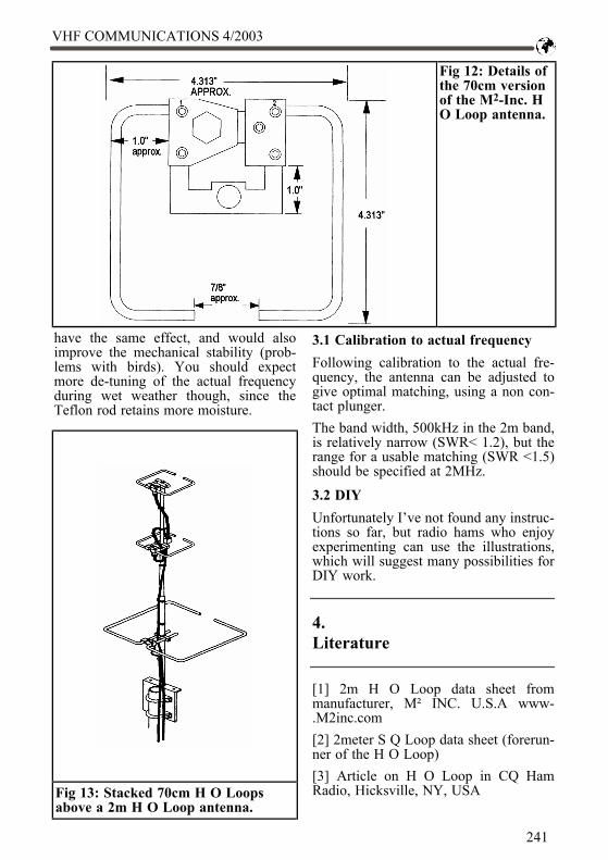
have the same effect, and would alsoimprove the mechanical stability (prob-lems with birds). You should expectmore de-tuning of the actual frequencyduring wet weather though, since theTeflon rod retains more moisture.
3.1 Calibration to actual frequencyFollowing calibration to the actual fre-quency, the antenna can be adjusted togive optimal matching, using a non con-tact plunger.The band width, 500kHz in the 2m band,is relatively narrow (SWR< 1.2), but therange for a usable matching (SWR <1.5)should be specified at 2MHz.
3.2 DIYUnfortunately I’ve not found any instruc-tions so far, but radio hams who enjoyexperimenting can use the illustrations,which will suggest many possibilities forDIY work.
4.Literature
[1] 2m H O Loop data sheet frommanufacturer, M² INC. U.S.A www-.M2inc.com[2] 2meter S Q Loop data sheet (forerun-ner of the H O Loop)[3] Article on H O Loop in CQ HamRadio, Hicksville, NY, USA
Fig 12: Details ofthe 70cm versionof the M2-Inc. HO Loop antenna.
Fig 13: Stacked 70cm H O Loopsabove a 2m H O Loop antenna.
VHF COMMUNICATIONS 4/2003
241
1.0Introduction
Rhe’os is Greek for “flow” and stato’s isGreek for “set” or “to set”. In Swedish,flow is ström, part of my name. Maybethat is what inspired the article...The word “Rheostat” is sometimes useda bit freely. Although I am sure mostreaders of VHF Communications knowsexactly what it is, maybe some do not.Let us make sure:• The Rheostat is a Resistor with one
end adjustable, or it is a Potentiom-eter where one end is left unused (orconnected to the wiper) see Fig 1.
At one time or another we have all burntup one end of a potentiometer as weconnected it as a Rheostat and tried tovary something drawing too much cur-rent! In Fig 2 we can see a Rheostat (oneend of the winding is not available),compared to a “normal” size potentiom-eter, able of handling maybe 50W overits full length. Clearly, it has got a bit toomuch, while only part of it was in circuit.This illustrates the nature of the problem.The Rheostat, described in this article,dissipates all the power in the entiredevice all the time! Be it 1µA or 10A.The Rheostat in the picture has a totalresistance of 24Ω. Its Max current wouldthen be 1.4A and it is clearly not of muchuse for currents less than some 0.1A or inexcess of a few amps.The problem is well known and obvious:A dial lamp for 6V 0.3A can be run froma 12V battery with a 20Ω resistor inseries. I may want to dim it as well, so Imay pick a 100Ω Potentiometer (con-nected as a Rheostat, not as a Potentiom-eter). When it is set for normal operation,6V x 0.3A = 1.8W is developed in thelamp and the same in the 1/5th of thepotentiometer in use (Fig 3). So, theentire potentiometer must be able tohandle 5 times as much, or 10W. Thiscertainly excludes any small Rheostat,maybe therefore the limited popularity ofthe variable resistor as a Rheostat. If thecurrents involved are yet higher, eitherthe available resistance must be lesser or
Carl G. Lodström, KQ6AX & SM6MOM
The noble art of the Rheostat
Fig 1: Resistor, Rheostat andPotentiometer.
VHF COMMUNICATIONS 4/2003
242

the power rating must be higher. ARheostat truly must be hand picked forthe application and selected with someskill. Neither is it a true Rheostat. If theavailable voltage, or the load resistance,varies, so will the set current.
2.0The true rheostat!
My solution to the problem can be set tocontrol currents in the µA range, as wellas in the tens of amperes by the turn of a
knob! This would normally call for aresistance range of some 1MΩ to 0.1Ω(or even less), and of course many totallydifferent devices! Perhaps as many as theseven magnitudes of current range.The Rheostat presented can also handlehundreds of volts and it can dissipatehundreds of watts (with a sufficient heatsink of course). As such it is superior toall normal variable resistors! The controlof this one is by means of a regular knob,on a regular potentiometer, easily turned.Have you ever tried to turn a huskyrheostat, rated 100W, with your finger-tips on a small knob?
2.1 Some ApplicationsOne very useful application is to chargebatteries with constant current (or todischarge them with the same to measuretheir capacity).To charge some NiCd batteries with aconstant 0.3A at up to 15V. Find a sourceof 15V, good for at least 0.3A. A wallplug adapter maybe. Connect the Rheo-stat in series and adjust for 0.3A (in shortcircuit or with the batteries in circuit)!There you are! Your batteries will becharged with 0.3A until the suppliedvoltage limits further increase.You have a diode that you want to use
Fig 2:Photograph of anormalpotentiometerand Rheostat.
Fig 3: Controlling a dial lamp.
VHF COMMUNICATIONS 4/2003
243
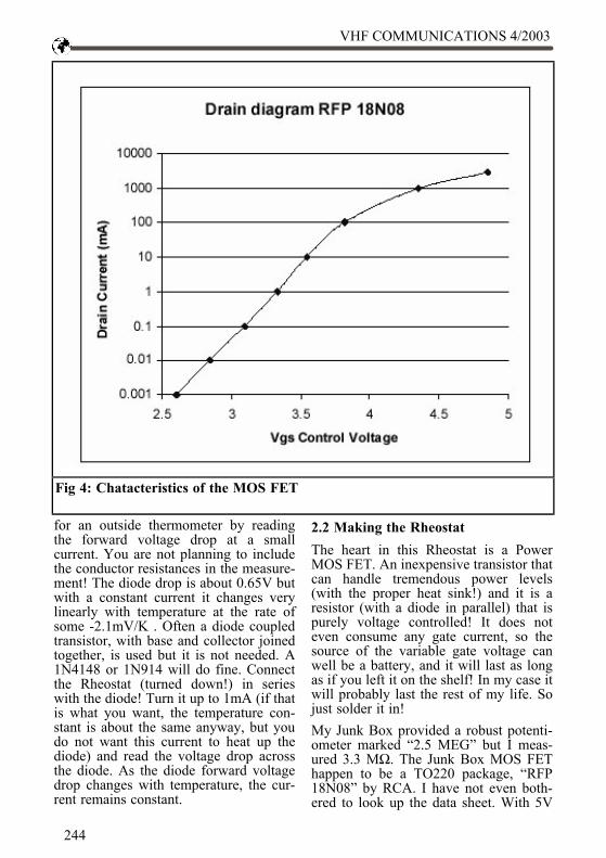
for an outside thermometer by readingthe forward voltage drop at a smallcurrent. You are not planning to includethe conductor resistances in the measure-ment! The diode drop is about 0.65V butwith a constant current it changes verylinearly with temperature at the rate ofsome -2.1mV/K . Often a diode coupledtransistor, with base and collector joinedtogether, is used but it is not needed. A1N4148 or 1N914 will do fine. Connectthe Rheostat (turned down!) in serieswith the diode! Turn it up to 1mA (if thatis what you want, the temperature con-stant is about the same anyway, but youdo not want this current to heat up thediode) and read the voltage drop acrossthe diode. As the diode forward voltagedrop changes with temperature, the cur-rent remains constant.
2.2 Making the RheostatThe heart in this Rheostat is a PowerMOS FET. An inexpensive transistor thatcan handle tremendous power levels(with the proper heat sink!) and it is aresistor (with a diode in parallel) that ispurely voltage controlled! It does noteven consume any gate current, so thesource of the variable gate voltage canwell be a battery, and it will last as longas if you left it on the shelf! In my case itwill probably last the rest of my life. Sojust solder it in!My Junk Box provided a robust potenti-ometer marked “2.5 MEG” but I meas-ured 3.3 MΩ. The Junk Box MOS FEThappen to be a TO220 package, “RFP18N08” by RCA. I have not even both-ered to look up the data sheet. With 5V
Fig 4: Chatacteristics of the MOS FET
VHF COMMUNICATIONS 4/2003
244

on the gate, the resistance was prettymuch bottomed out at a few tenths of anohm. This tells me two things: It is not aVery High Voltage device, or the resist-ance would have been higher. Neither isit a Very High Current device (50A orso) or the resistance would have beenlower, below 0.1Ω. The part numberprobably means 18A and 80V and that isfine with me. It is all I need for a generalpurpose Rheostat. There are other MOSFETs in the Junk Box should I needmore!I started out this project by taking a lookat the general character of the controlproperties of this transistor. Such a bigone would normally not be considered inthe µA range, but if it works there, whynot make a note of it? The Graph in Fig 4shows what Drain currents I got with a5V on the Source and for various Gate-Source voltages. The current was practi-cally constant, independent of the appliedSource voltage, for all currents up to 1Aor so, varying at most with 1% from lessthan 1V to over 20V.Clearly, 2V is sufficient to turn thistransistor completely off, and 5V enoughto turn it fully on. Maybe more than youwould want. This means that we want 2Vat the bottom of the Potentiometer (if we
plan to control such small currents).Across the pot, P1 (Fig 5), that in thiscase is 3.3MΩ, we would like to see 3V.This makes R1 = 2.2MΩ. Neither do wehave 5V batteries. Maybe we have a 9Vbattery? Or a 6V? Suffice it to say that,in this case, we can add 1.1MΩ perbattery voltage above 5V on top of thepotentiometer (R3). This helps keepingthe drain on the battery to lowest possi-ble current as well as making the “rangeof interest” equal the mechanical rangeof the potentiometer. You do not want allthe action at one end of the dial!We can see that for currents up to100mA it adheres beautifully to a loga-rithmic function. Above there I suspectthat the resistance in the Source leg (pinand bond wires) adds a voltage dropcounteracting the applied control voltageon the Gate. At 1A we can see that itshould have been about 4V, but it is4.35V. A resistance of 0.35Ω wouldexplain this, and this may very well bethe actual leg resistance + bond wire.This value will of course be different fordifferent transistors. By no means do Isuggest that this particular transistor isbetter than any other, I just happened tohave it laying around.If you use the newer MOS FETs with
Fig 5: The circuitdiagram of theRheostat.
VHF COMMUNICATIONS 4/2003
245
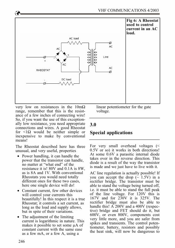
very low on resistances in the 10mΩrange, remember that this is the resist-ance of a few inches of connecting wire!So, if you want the use of this exception-ally low resistance, you need appropriateconnections and wires. A good Rheostatfor <1Ω would be neither simple orinexpensive to make by conventionalmeans!The Rheostat described here has threeunusual, and very useful, properties• Power handling, it can handle the
power that the transistor can handle,no matter at “what end” of theresistance it is! 80V and 0.1A is 8W,as is 8A and 1V. With conventionalRheostats you would need totallydifferent ones for these two cases,here one single device will do!
• Constant current, few other deviceswill control your currents thisbeautifully! In this respect it is a trueRheostat; it controls a set current, aslong as the load and supply allows,but in spite of their variations.
• The adjustment of the limitingcurrent is logarithmic in nature. Thismakes it possible to set some µA ofconstant current with the same easeas a few mA, or a few A, using a
linear potentiometer for the gatevoltage.
3.0Special applications
For very small overhead voltages (<0.5V or so) it works in both directions!At some 0.6V a parasitic internal diodetakes over in the reverse direction. Thisdiode is a result of the way the transistoris made and we just have to live with it.AC line regulation is actually possible! Ifyou can accept the drop (~ 1.5V) in arectifier bridge. The transistor must beable to stand the voltage being turned off,i.e. it must be able to stand the full peakof the line voltage. For 120V this is167V and for 230V it is 325V. Therectifier bridge must also be able tohandle this! A 200V and a 400V (respec-tive) bridge and FET should do it, but600V, or even 800V, components costvery little more, and you are safer fromspikes and transients. The control poten-tiometer, battery, resistors and possiblythe heat sink, will now be dangerous to
Fig 6: A Rheostatused to controlcurrent in an ACload.
VHF COMMUNICATIONS 4/2003
246

touch. If this is what you want to build,enclose it all in a metal box, use a safetyground, insulate the transistor from theheat sink with a mica washer and useonly in grounded outlets.In this application the transistor is con-nected with the Drain (usually also thetab on a TO220 or the body of a TO3package) to the + corner of the rectifierbridge and Source as well as the - side ofthe battery to the - corner. The two ACcorners are placed in series with the AC
source and the load (Fig 6).Beware of the power in this case, it canget very high very quickly! You mayhave 1A in the blink of an eye and with230V you also have 230W! Either yourheat sink is of a very good size or youwill not have a working Rheostat forvery long! For high powers several MOSFETs of the same kind can be paralleledwithout matching. This will also distrib-ute the heat more evenly over a heat sink.
Fig 7: Circuitdiagram of a fourterminalRheostst.
Fig 8: Photograph of the fourterminal Rheostat.
Fig 9: Photograph of the fourterminal Rheostat.
VHF COMMUNICATIONS 4/2003
247

3.1 RF concerns.Since the transistor has gain, it can bemade to oscillate. Probably not more thanat a few MHz, if even that, but it wouldresult in poor regulation. Since no cur-rent flows in the gate, a series resistorthere will not matter. A few kΩ in serieswith the gate lead, located near thetransistor body will ensure that no oscil-lation occur. Since the gate draws nocurrent, this has no other drawback.Another RF concern is the possible sensi-tivity to RFI from your transmitters. TheRheostat is not likely to be sensitive to it,but test! Especially for a case like using adiode for outdoor thermometer. The longconductors will act as an antenna andmay pick up enough for the diode torectify it, or for to carry it back to theMOS FET (which should not react, butone never knows!). Put an extra few100Ω in series with each conductor at theRheostat end, maybe a small capacitoracross the diode, and twist the long wireslightly, minimising pickup. The extraresistors will not affect the voltage dropacross the diode, as long as there isenough voltage available. If it is impor-tant that your equipment is insensitive toRF, as always, test it thoroughly beforeyou rely on it!
3.2 A four terminal RheostatA four terminal Rheostat can be built,which may be more practical for someapplications Figs 7,8 & 9). I found thecomponents at Radio Shack. Loud-speaker terminals are good for universaluse. Here I visualised the availability of apower supply (of more than 6.5V) so onewould not need the battery, although onecan keep that part of the design. Thebottom plate is also the heat sink for theMOS FET so it can only handle a fewwatts.In this one I used a 5V regulator,LM78L05 for the gate voltage. It needssome 6.5V in for regulation, and canhandle some 32V. If 5V is not enough
for your particular FET, use the LML08or 12V regulators! D not omit C1, 10 -100nF or so, because he regulator maythen well become an oscillator at a fewMHz! Not good for the performance!
4.0Conclusion
You will soon find a lot of applicationsfor this Rheostat, especially if yourpower supply does not have a currentlimiter.NiCd battery charging can be done witha transformer, a rectifier and the Rheostatas well! Assuming it is a full transformer(with a low voltage output), not an autotransformer, then safety is taken care of.If it has a 12V secondary, the peakvoltage is 17V, and for a light load, suchat the end of the charging cycle, it maywell be 5-10% more, 18V maybe. Therectifier bridge will take 2 x 0.7V, so16.6V is left, more than the 15V wewanted, so watch out! The current isconstant so the batteries will be charged,but you should have a voltmeter on themand remove them when the correct volt-age is reached. Naturally, the current willbe regulated but only when the rectifiedvoltage in is high enough! As the batter-ies charge, the conducting fraction of theperiod time will be less and less. So theaverage current becomes lower, possiblyonly flowing 30% of the time, and thus itmay appear as less than the set current onthe average, taking take more time thanyou thought to charge the battery. Aneasy way out of this, if it is important, isto put an electrolytic capacitor across theDC corners of the bridge. In our examplewe will now have an almost constant18V and the the set current will flow100% of the time! Even more reason tokeep an eye on the voltage, or thebatteries will be destroyed by overcharg-ing.
VHF COMMUNICATIONS 4/2003
248

I have noticed one thing with the Rheo-stat that is a potential problem for smallstuff. When the Rheostat "turned down",and one applies voltage to the circuit,there is a spike of higher current for a msor so until it regulates down the setcurrent. I assume this is due to the D-Gcapacitance, but have not delved into it.So, for small, sensitive loads, make surethe power source cannot deliver tran-sients! Somebody may be sitting andplaying around with crystal diodes orvery small light bulbs.... It works fine ifthe power is already applied to theRheostat to begin with, and it is turned itup.Real Potentiometers, or Rheostats can bevery large, Fig 10 shows “normal” sizePotentiometers. The Rheostat described
in this article (Figs 11 &12) can handleas much power, or more, than the largerone pictured.This article has described a profoundlysimple and versatile Rheostat with excel-lent performance and a low componentcount/cost. The power handling sets itapart as it can handle what the MOS FETand its heat sink allows over the entirerange. There is no “last few turns” ofresistance body in this Rheostat! Thecircuit makes the Rheostat a practicalpossibility and a rugged universal com-ponent capable of constant power dissi-pation regardless of resistance setting.There are a lot of uses for it in the wellequipped Shack!
Fig 10: Examplesof Potentiometersand Rheostats.
Fig 11: The author's Rheostat. Fig 12: The author's Rheostat.
VHF COMMUNICATIONS 4/2003
249

(Translators note: The German storycontained some dialogue in the Schwa-bian dialect, so I have exercised somepoetic licence and set the scene in Bir-mingham, with the Schwabian characterbecoming a Brummie.)
The following story is the result of afriendly agreement between the authorand the editor of UKW Berichte on thesubject of the “electronic essay”. Thequestion was whether there was roomin a technical periodical for anythingother than just technology in articleskept suitably technical. So what fol-lows is a sample, an incident from theeveryday life of a man with a passionfor electronics.
Today:The treasure trove of electronicscrap
It is a well known fact that we all havemany unalterable characteristics. How-ever, even today little is known, and littlescientific research has been done, intothe characteristics and genetic traits ofthe incorrigible tinkerer, who neverwalks past a scrap yard or a flea marketwithout investigating.In the electronics field, both the elec-
tronic scrap recycling companies and themiscellaneous amateur flea markets exerta magnetic attraction which no “realenthusiast” can withstand.According to my wife, Im not muchbetter. I neednt, and indeed cant seriouslydeny it! It was no accident that mystudents invented a new nickname for me(DIY Danny) a name my family some-how found out about (I still have no ideahow).
But to my tale:
Now and then you have to pause awhileand leave off the work, work, work, togive ones faithful spouse an unexpectedtreat. In our family this can mean, forexample, a day out to the big city, maybe100km away. For one thing, its my wifeshome town, and for another its where Icompleted my studies and then workedfor a few years afterwards (and yes,youre right, its where our lifelong part-nership began). When we get there, wepractice a new version of the maritalbreak-up: I leave my wife in the pedes-trian precinct for a couple of hours sothat she can have a good look round theshops without being hampered by animpatient husband. True, this is fre-quently expensive, but in these two hoursIm free to have a thorough rummagearound the 10 to 20 cubic metres of
Gunthard Kraus, DG8GB
Funny electronic stories
VHF COMMUNICATIONS 4/2003
250

circuit boards available in the electronicscrap recycling centre operated by aformer fellow student of mine. There Iam free to do what I like, and I alwaysfind something, since this recycling cen-tre takes in supplies from a radius of atleast 150km.When the two hours are up, I link upwith my spouse again and we spend therest of the day doing things together.This is a tried and tested system. Each ofus is usually extremely satisfied with hisor her finds, and I can certainly recom-mend this as a risk free technique toothers.But there was one occasion..... It wassometime last year, and the weather wasvery warm. It hadnt rained for a longtime and so for once the scrap yard didntlook like the normal bog. So there I wasrooting around in a box, when I noticedsomething was a bit out of place. Wholeareas of the ground were gleaming hereand there under the circuit boards! Itdefinitely wasnt water, and I wont tryand spin out the suspense. After aboutone hours digging, I was the proudpossessor of about 3kg of small, modern10MHz crystals, which had just beenchucked onto the big heap. Lets draw aveil over the foolish antics involved inreaching this position, since Id had to:
• shift vast quantities of scrap circuitboards
• use my fingers as if I was panningfor gold and plough through allthe dust, and then
• find a suitable container so that Icould carry the stuff away.
The final volume filled a 2 litre gherkinjar, I know this because I ended up usingthe said jar as a means of transport. Thefirst problem, of course, was the proprie-tor, my old fellow student, who asked me(as he was entitled to do): “What are youdoing with that then?” (actually he askedme in broad Brummie, so it soundedsomething like: “Warra yo doin wi
that?”). I mumbled some reply whichmight have been: “Dunno really” or “Ivegot a few ideas” or even: “I know lots ofpeople whore looking for this kind ofthing”. The scrap price to be paid wasminimal, about what youd pay if youordered two new crystals like this, VATand postage included.What might appear as the next problem,the wife, was not a problem at all sincethe first thing you do in this kind ofsituation is to wash your hands some-where and the next is to be absolutely ontime for the rendezvous. So her question:“Well, did you find anything nice oruseful?” could be answered in the af-firmative without any problems, and withgreat satisfaction.The scene now changes to the domestichome, a few hours later. What real DIYenthusiast could resist the attractions of agherkin jar like this? Not me! Tragically,this was where I forgot to pay attention,and suffered from an excess of enthusi-asm. For this led to a practical confirma-tion of something from my old physicstextbook:“The pain threshold for the human earlies at approximately 110 dBa”.Would you like to know the details? OKjust carelessly use the sacrosanct, ex-tremely new pasta strainer to wash about3 kilograms of filthy crystals in thesacrosanct stainless steel rinsing sink inthe sacrosanct kitchen....Fortunately, even in Nature every thun-derstorm and every hailstorm comes toan end and youre free to try out all thepossibilities of your new toys: from thequartz oscillator through the ladderquartz filter to the multiplier, you cansimulate and assemble the lot. But even-tually, there are no more games to play -and even your friends tend to start whenyou happen to meet them, afraid youregoing to ask them again whether theyneed any 10MHz crystals. The gherkinjar and its contents have a melancholylook, but something must be done with
VHF COMMUNICATIONS 4/2003
251

them. When everyone has been providedwith 10MHz crystals, Ill perhaps solderup most of them in a lead coffin and burythem somewhere as hidden treasure forour descendants to find. Perhaps in 200years time they wont know what crystalsare any more, and that will give thearchaeologists something to puzzle theirheads about.The question remains, dare one take therisk of going digging for gold in therecycling centre again and of finding newtreasures? Im reminded of another expe-rience which serves as a terrible warning.It was high Summer last year, and I wasscrabbling around on the circuit boardmountain 2 metres high (wearing birch-wood sandals and shorts), when thebeastly thing began to slide. Naturally, Ilost my sandals in the fall (that wasnt aproblem, I found them again!). But cir-
cuit boards fitted with components looklike beds of nails for Indian fakirs whenseen from below and I had to clamberover them to save myself. Dont ask mehow I explained the sudden and inexpli-cable disappearance of my socks to mywife (by the end, they were ripped topieces and smeared with blood), for Idont remember clearly what I said myselfany more. At all events, since then, to beon the safe side, Ive resisted the goldfever for quite some time, and confinedmyself to pottering about with compo-nents Ive already got handy at home.But now the itch is slowly gettingstronger again. For who knows what youmight find in the circuit board boxes thisvery day, right now?. And in the endthats a feeling that could wake a realDIYer even if he was hibernating for theWinter!
VHF COMMUNICATIONS 4/2003
252

Theory of Antennas
That’s the heading above the lists oflinks and downloads on this homepage.But we’re dealing with tutorials on thebasic principles here, the list is neverending, and it’s impossible to itemiseeverything there is here on this subject.So just have fun rummaging around!Address:http://members.fortunecity.com/ xe1bef/theory-antennas.htm
Radiometrix
A company which specialises, in particu-lar, on data transmission and modems,including those operating over radioroutes. But there are also some neatapplication notes for the RF freak, quiteapart from the many data sheets andother information regarding interfaces.Address:http://www.radiometrix.com/
TX Lines, Antenna Systems, PCJoystick
We don’t want to spend all our time
talking about antennas, but a homepagewith such good tutorials and with somany different applications deserves amention.Address:http://www.tmeg.com/tutorials/tutori-als.htm
Radio Waves
The site’s name gives you a pretty goodclue: it deals with developments andproducts relating to electromagneticwaves. The main theme is antenna devel-opment and the production of completeantenna arrays. And because in this kindof work you have to pay very closeattention to the customer’s wishes,there’s also an extensive planning sec-tion. One splendidly attractive gift fromthese people to all RF freaks is the “RWcalculator” for calculating and planningevery last little thing relating to antennasand receivers, which you can downloadfree of charge. This is really somethinggreat, with many different applications ofall kinds!Address:http://www.radiowavesinc.com/html/414_rf_system_planning_tools.cfm
Gunthard Kraus, DG8GB
Internet Treasure Trove
VHF COMMUNICATIONS 4/2003
253

Longwave links
Just for a change, here’s something inGerman, and something for the commu-nity of longwave fans. This homepage isa must for anyone wanting to know moreabout this field and this technology.Address: http://home.t-online.de/home/h-hcuno/afu/ longlink.htm
Amateur Television and highspeed data signalling
Even though this homepage is hostedfrom France, you don’t need any knowl-edge of French, as there is an Englishversion. We are certainly grateful to theowner for the opportunity to downloadinformation on well documented DIYprojects, going up to 2.3GHz, which willgladden the heart of any do-it-yourselfer.Address:http://perso.wanadoo.fr/jf.fourcadier/ac-cueil/accueil_e.htm
G4FGQ’s Software Site
An interesting page, put together in away that’s just right for the amateur andfor anyone who likes fiddling about withRF projects. You can spend a lot of timehere searching, investigating and down-loading. Most of this site is about pro-grams, all “home made” and all similar inappearance. So you know at once whatit’s all about, and you don’t have tospend a long time in experimental opera-tions. Very rewarding and highly recom-mended!Address:http://www.btinteret.com/~g4fgq.regp/#S102
W2BRI’s Magnetic Loop Siteand PA3CQR magnetic loopantenna page
As always on such sites, the more younose around and the more stones youturn over, the more treasures you un-earth. Very enjoyable and informative tosee everything concerning loop antennassummarised here.Addresses:http://www.standpipe.com/w2bri/index-.htmhttp://www.iri.tudelft.nl/~geurink/magn-loop.htm
Alphabetically arranged radiotechnology links
A site like this makes it considerablyeasier and more comfortable to search fora program, an article or a homepage tosolve a problem.Address: http://home.wanadoo.nl/~a.s-chipper/fuurllinks.htm
Myer’s Engineering Interna-tional
23 years of experience with radio com-munication systems and antennas... that’swhat it says in the introduction to thissite. Another homepage which can revealmasses of new or fascinating facts forthose with an interest in such matters.Seek, and ye shall find...Address:http://www.myerseng.com/index.html
VHF COMMUNICATIONS 4/2003
254

Back IssuesAll issues ever published now available aseither photocopies or actual magazines.Issues from 1/1969 to 4/2001 are £1.00each + postage. Issues from 1/2002 to4/2002 are £4.70 each or £18.50 for all 4issues + postage. See web site for backissue list to see which issues are onlyavailable as photocopies.
Blue BindersThese binders hold 12 issues (3 years) andkeep your library of VHF Communica-tions neat and tidy. You will be able tofind the issue that you want easily. Bindersare £6.50 each + postage. (UK £0.90,Surface mail £1.60, Air mail to Europe£2.00, Air mail outside Europe £3.60)
PUFF Version 2.1 Microwave CADSoftware
This software is used by many authors ofarticles in VHF Communications. It issupplied on 3.5 inch floppy disc with a fullEnglish handbook. PUFF is £20.00 +postage. (UK £1.00, Surface mail £1.30,Air mail to Europe £1.50, Air mail outsideEurope £2.50)
VHF Communications Web Sitewww.vhfcomm.co.uk
Visit the web site for more information onprevious articles. There is a full indexfrom 1969 to the present issue, it can besearched on line or downloaded to your
own PC to search at your leisure. If you want to purchase back issues,kits or PUFF there is a secure order form or full details of how to contactus. The web site also contains a very useful list of site links, anddownloads of some previous articles and supporting information.
VHF COMMUNICATIONS 4/2003
255

AUSTRALIA - Mark Spooner c/o, W.I.A. SA/NT Division, GPOBox 1234, Adelaide, SA 5001, Australia. Tel/Fax: 08 8261 1998BELGIUM - UKW-BERICHTE, POB 80, D-91081 BAIERSDORF,Germany. Tel: 09133-77980. Fax: 09133-779833 .Postgiro Nbg. 30445-858.DENMARK - KM PUBLICATIONS , 63 Ringwood Road,LUTON, LU2 7BG, UK. Tel: +44 1582 581051.Fax: +44 1582 581051. Email: [email protected] - Christiane Michel F5SM, Les Pillets, 89240 PARLY,FranceFax: (33) 03 86 44 08 82 Tel: (33) 03 86 44 06 91FINLAND - KM PUBLICATIONS , 63 Ringwood Road, LUTON,LU2 7BG, UK. Tel: +44 1582 581051.Fax: +44 1582 581051. Email: [email protected] - UKW-BERICHTE, POB 80, D-91081BAIERSDORF, Germany. Tel: 09133 7798-0. Fax: 09133 779833.GREECE - KM PUBLICATIONS , 63 Ringwood Road, LUTON,LU2 7BG, UK. Tel: +44 1582 581051.Fax: +44 1582 581051. Email: [email protected] - KM PUBLICATIONS , 63 Ringwood Road, LUTON,LU2 7BG, UK. Tel: +44 1582 581051.Fax: +44 1582 581051. Email: [email protected] - R.F. Elettronica di Rota Franco, Via Dante 5 - 20030Senago, MI, ItalyFax 0299 48 92 76 Tel. 02 99 48 75 15NEW ZEALAND - KM PUBLICATIONS , 63 Ringwood Road,LUTON, LU2 7BG, UK. Tel: +44 1582 581051.Fax: +44 1582 581051. Email: [email protected] - WAVELINE AB, Box 60224, S-216 09 MALMÖ,Sweden. Tel: +46 40 16 42 66. Fax: +46 40 15 05 07.GSM: 0705 16 42 66e-mail: [email protected] http://www.algonet.se/~wavelineSOUTH AFRICA - KM PUBLICATIONS , 63 Ringwood Road,LUTON, LU2 7BG, UK. Tel: +44 1582 581051.Fax: +44 1582 581051. Email: [email protected] & PORTUGAL - JULIO A. PRIETO ALONSO EA4CJ,Donoso Cortes 58 5° -B, MADRID 15, Spain. Tel: 543 83 84SWEDEN - WAVELINE AB, Box 60224, S-216 09 MALMÖ,Sweden. Tel: 040 16 42 66. Fax: 040 15 05 07. GSM: 0705 16 4266 e-mail: [email protected] http://www.algonet.se/~wavelineSWITZERLAND - KM PUBLICATIONS , 63 Ringwood Road,LUTON, LU2 7BG, UK. Tel: +44 1582 581051.Fax: +44 1582 581051. Email: [email protected] KINGDOM - KM PUBLICATIONS , 63 Ringwood Road,LUTON, LU2 7BG, UK. Tel: +44 1582 581051.Fax: +44 1582 581051. Email: [email protected]. - GENE HARLAN, ATVQ Magazine, 5931 Alma Drive,Rockford, IL 61108, USA. Tel: Toll free USA only: 800 557 9469;Elsewhere: +1 815 398 2683; Fax: +1 815 398 2688Email: [email protected] - KM PUBLICATIONS, address as for the U.K.
WWW: http://www.vhfcomm.co.uk
KM PUBLICATIONS,63 Ringwood Road, Luton,LU2 7BG, United KingdomTel: +44 1582 581051Fax: +44 1582 581051
Email:[email protected]
Andy Barter G8ATDThe international edition of theGerman publication UKW-Berichteis a quarterly amateur radiomagazine, especially catering forthe VHF/UHF/SHF technology.It is owned and published in theUnited Kingdom in Spring,Summer, Autumn and Winter byKM PUBLICATIONS.The 2003 subscription price is£20.60, or national equivalent.Individual copies are available at£5.15, or national equivalent each.Subscriptions should be addressedto the national representative shownin the next column. Orders forindividual copies of the magazine ,back issues, kits, binders, or anyother enquiries should be addresseddirectly to the publishers.NOTICE: No guarantee is giventhat the circuits, plans and PCBdesigns published are free ofintellectual property rights.Commercial supply of these designswithout the agreement of theAuthor and Publisher is notallowed. Users should also takenotice of all relevant laws andregulations when designing,constructing and operating radiodevices.
All rights reserved. Reprints,translations, or extracts only withthe written approval of thepublishersTranslated by: Inter-Ling Services,62 Caldecott Street, Rugby,CV21 3TH, UKPrinted in the United Kingdom by:Cramphorn Colour Printers Ltd.,15a Boughton Road IndustrialEstate, Rugby CV21 1BQ, UK.
Publishers
Editor
VHFCOMMUNICATIONS
© KMPUBLICATIONS
ISSN 0177-7505
A Publication for the Radio Amateur Worldwide
Especially Covering VHF, UHF and Microwaves
Volume No.35 Winter Edition 2003-Q4
VHFCOMMUNICATIONS

The microwave bands are an excellent area for radioamateurs who want to experiment and construct their ownequipment. The RSGB in partnership with the ARRL hasproduced this invaluable source of reference information forthose interested in this area, along with excellent designsfrom around the world to fire the imagination. Material hasbeen drawn from many sources including the RSGB journalRadCom and the ARRL publications QST & QEX. Along-side this material a truly international range of sources havebeen used including items from Germany, Denmark, NewZealand, Slovenian and many more.The earlier chapters of the book provide invaluable refer-ence material required by all interested in this exciting areaof experimentation. Techniques and devices are covered indepth, leading the reader to understand better the widerange of equipment and techniques now available to themicrowave experimenter. This book contains a wide selec-tion of designs using the latest technology that canreasonably be used by radio amateurs and ranges from onesthat can be reproduced by most radio amateurs to those thatrequire a high degree of skill to make.
With the explosion in consumer electronics using microwave frequencies the opportunity toexperiment has never been greater and this book is simply the best guide to the area of microwaveradio.
Available in the UK for £24.99 from www.rsgb.org/shop and in theUSA for $39.95 from www.arrl.org ISBN 1-872309-83-6
The International Microwave Handbook
Microwave Projects is aimed at those who are interested inbuilding equipment for the amateur radio microwave bands.Packed full of ideas from around the world this book coversthe subject with a variety of projects. The book has manycontributors who have a wealth of experience in this areaand they have produced many projects, design ideas,complete designs and modifications of commercial equip-ment, for the book.This title provides much useful information as to what canbe achieved effectively and economically. Aimed at boththe relative novice and the "old hand" the book also coversuseful theory of designing microwave circuit and testequipment for the projects. The book includes chapterscovering:
• Signal Sources • Transverters • Power Amplifiers• Test Equipment • Design
Microwave projects is a must have book for all those whoare already active on the microwave bands and thoselooking for interesting projects to embark on.
Available for £14.99 from www.rsgb.org/shop ISBN 1-872309-90-9
Microwave Projects

COMPLETE KITS, PCB's & ICs ARE AVAILABLEFOR RECENT PROJECTS
If the kit or PCB is not in this list please contact K. M. Publications
READY MADE DESCRIPTION ISSUE No. PRICEDG6RBP Pre Divider (:10) up to 5GHz 1/02 £ 140.00DG6RBP ATV Squelch 4/02 06006 £ 55.00
KIT DESCRIPTION ISSUE No. PRICEDJ8ES-019 Transverter 144/28MHz 4/93 06385 £ 120.00DJ8ES-019/50 Transverter 50/28MHz 2/95 06392 £ 120.00DJ8ES-020/50 10W PA for 50MHz 2/95 £ 140.00DJ8ES-047 Log Amplifier up to 500MHz with AD8307 2/00 06571 £ 42.00DG6RBP-002 Pre Divider (:10) up to 5GHz 1/02 £ 115.00DB6NT-Rotor Simple Speed Control for Rotators 2/02 06533 £ 35.00
PCB DESCRIPTION ISSUE No. PRICEDJ8ES-019 Transverter 144/28MHz or 50/28MHz 4/93 06384 £ 10.00S53MV Set of PCBs for Matjaz Vidmar Spectrum Analyser 4/98-4/99 S53MV £ 65.00DJ8ES-047 Log Amplifier up to 500MHz using AD8307 2/00 06569 £ 6.50DG6RBP-002 Pre Divider (:10) up to 5GHz 1/02 £ 18.00DJ8ES-053 Frequency Generator to 4GHz - mixer 1/02 £ 10.50DJ8ES-054 Frequency Generator to 4GHz - oscillator 1/02 £ £9.50DJ8ES-054 Frequency Generator to 4GHz - microcontroller 1/02 £ 15.50DB6NT-Rotor Simple Speed Control for Rotators 2/02 06532 £ 5.50DJ8ES-056 Speech Store With Integrated Sequencer 2/02 £ 7.00DG6RBP ATV Squelch 4/02 06542 £ 3.50
ICs DESCRIPTION ISSUE No. PRICEDJ8ES AT90S2313 For Digital Speech Store 2/02 £ 17.25DJ8ES/DL5HAT AT89C52 For GPS Control Of 10 MHz Standard 1/01 10353 £ 21.50
Please note that due to component supply problems some items have along delivery time, please ask for advice on delivery.
Minimum shipping charge £5.00K. M. Publications, 63 Ringwood Road, Luton, Beds, LU2 7BG, U.K.
Tel / Fax +44 1582 581051 email [email protected] Site http://www.vhfcomm.co.uk