maharashtra state board of technical education … · circuit. 7 at resonance, the series rlc...
TRANSCRIPT

MAHARASHTRA STATE BOARD OF TECHNICAL EDUCATION
(Autonomous)
(ISO/IEC-27001-2005 Certified) __________________________________________________________________________________________
Winter – 2017 Examinations
Model Answer Subject Code: 17323 (ECN)
Page No :1 of 26
Important Instructions to examiners:
1) The answers should be examined by key words and not as word-to-word as given in the model answer
scheme.
2) The model answer and the answer written by candidate may vary but the examiner should assess the
understanding level of the candidate.
3) The language errors such as grammatical, spelling errors should not be given importance (Not applicable
for subject English and Communication Skills).
4) While assessing figures, examiner may give credit for principal components indicated in the figure. The
figures drawn by candidate and model answer may vary. The examiner should give credit for any
equivalent figure/figures drawn.
5) Credits to be given step wise for numerical problems. In some cases, the assumed constant values may
vary and there may be some difference in the candidate’s answers and model answer (as long as the
assumptions are not incorrect).
6) In case of some questions credit may be given by judgment on part of examiner of relevant answer based
on candidate’s understanding.
7) For programming language papers, credit may be given to any other program based on equivalent
concept

MAHARASHTRA STATE BOARD OF TECHNICAL EDUCATION
(Autonomous)
(ISO/IEC-27001-2005 Certified) __________________________________________________________________________________________
Winter – 2017 Examinations
Model Answer Subject Code: 17323 (ECN)
Page No :2 of 26
1 Attempt any TEN of the following: 20
1 a) Define cycle and time period related to a. c. waveform.
Ans:
i) Cycle:
A complete set of variation of an alternating quantity which is repeated at
regular interval of time is called as a cycle.
OR
Each repetition of an alternating quantity recurring at equal intervals is
known as a cycle.
ii) Time Period:
Time period of an alternating quantity is defined as the time required for
an alternating quantity to complete one cycle.
1 Mark
1 Mark
1 b) Define active power and reactive power for R-L-C series circuit.
Ans:
Active power and reactive power for R-L-C series circuit:
(i) Active Power (P):
Active power (P) is given by the product of voltage, current and the
cosine of the phase angle between voltage and current.
Unit: watt (W) or kilo-watt (kW) or Mega-watt (MW)
watt
(ii) Reactive Power (Q):
Reactive power (Q) is given by the product of voltage, current and the
sine of the phase angle between voltage and current.
Unit: volt-ampere-reactive (VAr), or kilo-volt-ampere-reactive (kVAr) or
Mega-volt-ampere-reactive (MVAr)
volt-amp-reactive
1 Mark
1 Mark
1 c) Draw impedance triangle and voltage phasor diagram for R-L series circuits.
Ans:
1 Mark
For each
= 2 Marks
1 d) Define susceptance and admittances for a parallel circuit.
Ans:
Susceptance (B):
Susceptance is defined as the imaginary part of the admittance.
It is expressed as,
In DC circuit, the reactance is absent, hence X = 0 and susceptance becomes
equal to zero.
Admittance (Y):
Admittance is defined as the ability of the circuit to carry (admit) alternating
1 Mark
1 Mark

MAHARASHTRA STATE BOARD OF TECHNICAL EDUCATION
(Autonomous)
(ISO/IEC-27001-2005 Certified) __________________________________________________________________________________________
Winter – 2017 Examinations
Model Answer Subject Code: 17323 (ECN)
Page No :3 of 26
current through it. It is the reciprocal of impedance Z. i.e Y = 1/Z.
If impedance is expressed as , then the admittance is obtained as,
(Equations are
optional)
1 e) State superposition theorem applied to D.C. circuits.
Ans:
Superposition Theorem applied to D.C. circuits:
Superposition theorem states that in any linear, bilateral, multisource
network, the response (voltage across any element or current through any
element) of any branch is equal to the algebraic sum of the responses produced in
it with each source acting alone, while the other sources are replaced by their
internal resistances.
OR
Any other valid statement
2 Marks
1 f) State maximum power transfer theorem for DC circuit.
Ans:
Maximum power transfertheorem for DC circuit: The maximum power transfer theorem states that the source or a network
transfers maximum power to load only when the load resistance is equal to the
internal resistance of the source or the network.
The internal resistance of the network is the Thevenin equivalent resistance of
the network seen between the terminals at which the load is connected when:
i) The load is removed (disconnected)
ii) All internal independent sources are replaced by their internal resistances.
2 Marks
1 g) Write down the units of R, L, C and G
Ans:
Units of R, L, C and G:
R - ohm L – henry C – farads G - siemens or mho
½ mark each
=2 Marks
1 h) Define Quality factor of series AC circuit.
Ans:
Quality Factor of Series AC circuit:
The quality factor basically represents a figure of merit of a component (practical
inductor or capacitor) or a complete circuit. It is a dimensionless number and
defined as: *
+
OR In series circuit it is defined as voltage magnification in the circuit at resonance
OR It is also defined as the ratio of the reactive power of either the inductor or the
capacitor to the average power of the resistor.
√
2 Marks

MAHARASHTRA STATE BOARD OF TECHNICAL EDUCATION
(Autonomous)
(ISO/IEC-27001-2005 Certified) __________________________________________________________________________________________
Winter – 2017 Examinations
Model Answer Subject Code: 17323 (ECN)
Page No :4 of 26
1 i) How current source can be converted into equivalent voltage source?
Ans:
Conversion of current source into equivalent voltage source:
Rsh Vs
I
Rs
+
_
Is
Vs
v
current source equivalent voltage source
Find magnitude of equivalent voltage source, V = I × Rsh
Find magnitude of internal resistance of equivalent voltage source
Rs = Rsh
1 Mark
1 Mark
1 j) Draw the sinusoidal waveform of 3 phase emf and also indicate the phase
sequence.
Ans:
Phase sequence is R-Y-B
1½ Marks
½ Mark
1 k) Find frequency and RMS value of following voltage waveform refer Fig. No.1
Ans:
Frequency (f)
RMS Value V
√
1 Mark
1 Mark
1 l) State the behavior of following elements at the time of switching i.e. transient
period. - i) Pure L ii) Pure C
Ans:
Behavior of pure L at the time of switching i.e. transient period:
i) The pure inductor, carrying zero current prior to switching, acts as
OPEN CIRCUIT.

MAHARASHTRA STATE BOARD OF TECHNICAL EDUCATION
(Autonomous)
(ISO/IEC-27001-2005 Certified) __________________________________________________________________________________________
Winter – 2017 Examinations
Model Answer Subject Code: 17323 (ECN)
Page No :5 of 26
OR
ii) The pure inductor, carrying some current, say I0, prior to switching,
acts as a current source I0 or an Open Circuit in parallel with current
source I0.
Behavior of pure C at the time of switching i.e.transient period:
i) The pure capacitor, having zero voltage prior to switching, acts as
SHORT CIRCUIT.
ii) The pure capacitor, having some voltage, say V0, prior to switching,
acts as a voltage source V0 or Short Circuit in series with voltage
source V0.
.
1 Mark
1 Mark
2 Attempt any FOUR of the following: 16
2 a) Draw waveform and vector diagram to show following voltage and current.
V = 100 sin wt, and I = 4 sin (wt - 30)
Ans:
In vector diagram, RMS values have been shown.
2 Marks for
waveform
2 Marks for
vector diagram
2 b) Compare series and parallel circuits on any six points.
Ans:

MAHARASHTRA STATE BOARD OF TECHNICAL EDUCATION
(Autonomous)
(ISO/IEC-27001-2005 Certified) __________________________________________________________________________________________
Winter – 2017 Examinations
Model Answer Subject Code: 17323 (ECN)
Page No :6 of 26
Comparison between Series and Parallel Circuits:
Sr.
No.
Series Circuit Parallel Circuit
1
2
A series circuit is that circuit in
which the current flowing
through each circuit element is
same.
A parallel circuit is that circuit in
which the voltage across each
circuit element is same.
3
The sum of the voltage drops in
series resistances is equal to the
applied voltage V.
V = V1+V2+V3
The sum of the currents in
parallel resistances is equal to the
total circuit current I.
I = I1+I2+I3
4
The effective resistance R of the
series circuit is the sum of the
individual resistances connected
in series.
The reciprocal of effective
resistance R of the parallel circuit
is the sum of the reciprocals of
the individual resistances
connected in parallel.
5
For series R-L-C circuit, the
resonance frequency is,
√
For parallel R-L-C circuit, the
resonance frequency is,
√
6
At resonance, the series RLC
circuit behaves as purely resistive
circuit.
At resonance, the parallel RLC
circuit behaves as purely resistive
circuit.
7 At resonance, the series RLC
circuit power factor is unity.
At resonance, the Parallel RLC
circuit power factor is unity.
8
At resonance, the series RLC
circuit offers minimum total
impedance Z = R
At resonance, the parallel RLC
circuit offers maximum total
impedance Z =L/CR
9
At resonance, series RLC circuit
draws maximum current from
source, I = (V/R)
At resonance, parallel RLC circuit
draws minimum current from
source,
[ ⁄ ]
10
At resonance, in series RLC
circuit, voltage magnification
takes place.
At resonance, in parallel RLC
circuit, current magnification
takes place.
11
The Q-factor for series resonant
circuit is
√
The Q-factor for parallel resonant
circuit is,
√
4 Marks for
any 6 points
(
Marks for
each point)

MAHARASHTRA STATE BOARD OF TECHNICAL EDUCATION
(Autonomous)
(ISO/IEC-27001-2005 Certified) __________________________________________________________________________________________
Winter – 2017 Examinations
Model Answer Subject Code: 17323 (ECN)
Page No :7 of 26
12 Series RLC resonant circuit is
Accepter circuit.
Parallel RLC resonant circuit is
Rejecter circuit.
2 c) An alternating voltage of 250 V, 50 Hz is applied to a coil which takes 5A of
current, the power absorbed by the circuit is 1 kW. Find the resistance and
inductance of the coil.
Ans:
Given: V = 250V, f = 50Hz, I = 5A, P = 1 kW
P = VI
.ˑ.
.ˑ.
1 Mark for Z
1 Mark for R
1 Mark for XL
1 Mark for L
2 d) Derive the expression for resonance frequency for R-L-C series circuit.
Ans:
The frequency at which the net reactance of the series circuit becomes zero, is
called the resonant frequency fr.
Its value can be found as under:
At resonance XL - XC = 0 or XL=XC ωrL = 1/ωrC
ωr2=1/LC
.`. (2 π fr)2
= LC
√
1 Mark
1 Mark
1 Mark
1 Mark
2 e) Draw the phasor diagram and waveforms of voltage, current and power in a pure
inductance circuit supplied by a 1-phase a.c. source.
Ans:
Phasor diagram and waveforms of purely inductive circuit:
1 Mark for
Phasor
diagram
1Mark for
each
Waveform of
V, I, P

MAHARASHTRA STATE BOARD OF TECHNICAL EDUCATION
(Autonomous)
(ISO/IEC-27001-2005 Certified) __________________________________________________________________________________________
Winter – 2017 Examinations
Model Answer Subject Code: 17323 (ECN)
Page No :8 of 26
2 f) Compare series and parallel circuit.
Ans:
Sr.
No. Series Circuit Parallel Circuit
1
2
A series circuit is that circuit in
which the current flowing
through each circuit element is
same.
A parallel circuit is that circuit
in which the voltage across
each circuit element is same.
3
The sum of the voltage drops in
series resistances is equal to the
applied voltage V.
V = V1+V2+V3
The sum of the currents in
parallel resistances is equal to
the total circuit current I.
I = I1+I2+I3
4
The effective resistance R of the
series circuit is the sum of the
resistance connected in series.
The reciprocal of effective
resistance R of the parallel
circuit is the sum of the
reciprocals of the resistances
connected in parallel.
5
√
For series R-L-C circuit, the
resonance frequency is,
√
For parallel R-L-C circuit, the
resonance frequency is,
6
At resonance, the series RLC
circuit behaves as purely
resistive circuit
At resonance, the parallel RLC
circuit behaves as purely
resistive circuit.
7 At resonance, the series RLC
circuit power factor is unity.
At resonance, the Parallel RLC
circuit power factor is unity.
8
At resonance, the series RLC
circuit offers minimum total
impedance Z = R
At resonance, the parallel RLC
circuit offers maximum total
impedance Z =L/CR
9
At resonance, series RLC
circuit draws maximum current
from source, I = (V/R)
At resonance, parallel RLC
circuit draws minimum current
from source,
[ ⁄ ]
10
At resonance, in series RLC
circuit, voltage magnification
takes place.
At resonance, in parallel RLC
circuit, current magnification
takes place.
11 The Q-factor for series resonant
circuit is
The Q-factor for parallel
resonant circuit is,
1 Mark for
each of any 4
points
= 4 Marks

MAHARASHTRA STATE BOARD OF TECHNICAL EDUCATION
(Autonomous)
(ISO/IEC-27001-2005 Certified) __________________________________________________________________________________________
Winter – 2017 Examinations
Model Answer Subject Code: 17323 (ECN)
Page No :9 of 26
√
√
12 Series RLC resonant circuit is
Accepter circuit.
Parallel RLC resonant circuit
is Rejecter circuit.
3 Attempt any FOUR of the following: 16
3 a) A choke coil has a resistance of 2 Ω and an inductance of 0.035H is connected in
parallel with a 350F capacitor which is in series with a resistance of 20 Ω.
When combination is connected across a 200V, 50Hz supply.
Calculate:
i) The total current taken and
ii) Power factor of whole circuit Ans:
Given: R1 = 2 Ω L = 0.035H R2 = 20 Ω C = 350F
Z1 = R1 + j XL = (2 + j11) = 11.18 79.89 Ω
Z2 = R2 - j XC = (20 - j9.09) = 21.96 -24.44 Ω
Branch 1 current is given by,
= 17.88-79.89A = (3.138 – j17.60) A
Branch 2 current is given by,
=
9.107 24.44A = (8.29 + j3.76) A
Total current is,
I = I1 + I2 = (3.138 – j17.60) + (8.29 + j3.76)
i) I = (11.428 - j13.84)A = 17.94-50.45 A
( I can be calculated by considering equivalent impedance also)
ii) lagging
½ Mark for XL
½ Mark for XC
½ Mark for Z1
½ Mark for Z2
½ Mark for I1
½ Mark for I2
½ Mark for I
½ Mark for pf
3 b) A coil having resistance of 5Ω and inductance of 0.2H is arranged in parallel
with another coil having resistance of 1Ω and inductance of 0.08H. Calculate the
current through the combination and power absorbed when voltage of 100V,
50Hz is applied. Use impedance method.
Ans:
Given: R1 = 5 Ω L1 = 0.2H R2 = 1 Ω L2 = 0.08H
Branch 1
Branch 2
½ Mark
½ Mark
1 Mark

MAHARASHTRA STATE BOARD OF TECHNICAL EDUCATION
(Autonomous)
(ISO/IEC-27001-2005 Certified) __________________________________________________________________________________________
Winter – 2017 Examinations
Model Answer Subject Code: 17323 (ECN)
Page No :10 of 26
i) Current through the combination
amp
ii) Power absorbed
1 Mark
1 Mark
3 c) Define the following terms:
(i) Leading quantity
(ii) Lagging quantity Ans:
When two alternating quantities attain their respective zero or peak values
simultaneously, the quantities are said to be in-phase quantities.
When the quantities do not attain their respective zero or peak values
simultaneously, then the quantities are said to be out-of-phase quantities.
Leading Quantity:
The quantity which attains the respective zero or peak value first, is called
‘Leading Quantity’.
Lagging Quantity:
The quantity which attains the respective zero or peak value later, is called
‘Lagging Quantity’.
In above diagram, it is seen that for inductive circuit, the current is lagging
behind the voltage or the voltage is said to be leading the current.
Similarly, for capacitive circuit, the current is leading the voltage or the voltage
is said to be lagging behind the current.
2 marks for
diagram
1 Mark
1 Mark

MAHARASHTRA STATE BOARD OF TECHNICAL EDUCATION
(Autonomous)
(ISO/IEC-27001-2005 Certified) __________________________________________________________________________________________
Winter – 2017 Examinations
Model Answer Subject Code: 17323 (ECN)
Page No :11 of 26
3 d) A RC series circuit consisting of R = 10 Ω, C = 100 μF is connected across
200V, 50Hz AC supply. Find the value of current and power factor. What will be
the value of current and power factor if the value of resistance is doubled?
Ans:
Given: R = 10Ω, C = 100μF, V = 200V, f = 50 Hz
Capacitive reactance
Circuit Impedance
Current
amp
Power factor
If the resistance is doubled, then R = 20 Ω
Circuit Impedance
Current
amp
Power factor
1 Mark for XC
1 Mark for
current
½ Mark for
cos
1 Mark for
current
½ Mark for
cos
3 e) A 200W, 100V lamp is connected in series with a capacitor to a 120V, 50Hz AC
supply. Calculate:
i) The capacitance required
ii) The phase angle between voltage and current
Ans:
Given: Power rating of lamp P = 200W
Rated voltage of lamp VR = 100V
Supply voltage V = 120V, Frequency f = 50Hz
1) Capacitance required:
The value of capacitance should be such that rated voltage of 100V appears
across the lamp and lamp consumes rated power of 200W.
For rated power consumption in lamp, the required current be,
Impedance required to draw this current from 120V supply,
Capacitive reactance √ √
Power loss in the circuit
1 Mark for R
1 Mark for Z
1 Mark for C

MAHARASHTRA STATE BOARD OF TECHNICAL EDUCATION
(Autonomous)
(ISO/IEC-27001-2005 Certified) __________________________________________________________________________________________
Winter – 2017 Examinations
Model Answer Subject Code: 17323 (ECN)
Page No :12 of 26
Phase angle between voltage and current,
1 Mark for
3 f) State the relation between line and phase values of current and voltage for star
and delta connection.
Ans:
Star Connection:
√
i.e √
i.e
Delta Connection:
i.e
√
i.e √
1 Mark
1 Mark
1 Mark
1 Mark
4 Attempt any FOUR of the following: 16
4 a) Three coils each with resistance of 10Ω and inductance of 0.35mH are connected
in star to a 3-phase, 440V, 50Hz supply. Calculate the line current and total
power taken per phase.
Ans:
Data Given:
Line voltage VL = 440V, f = 50Hz
Resistance per phase R = 10Ω
Inductance per phase L = 0.35mH
Inductive reactance per phase
Zph = (10+j0.11) = 10.00060.63
In star connected load VL = √ and IL = IPh
√
√ 254.03V
(i) Line Current
(ii) Power factor cosϕ =
= 0.999
(iii) Power taken per phase P = VPh IPh cosϕ
= (254.03)(25.4)(0.999)
= 6445.909 W
1 Mark
1 Mark
1 Mark
1 Mark
4 b) State any four advantages of polyphase circuit over single phase circuit.
Ans:
Advantages of Polyphase circuit over Single phase circuit:
i) Three-phase transmission is more economical than single-phase
transmission. It requires less copper material.

MAHARASHTRA STATE BOARD OF TECHNICAL EDUCATION
(Autonomous)
(ISO/IEC-27001-2005 Certified) __________________________________________________________________________________________
Winter – 2017 Examinations
Model Answer Subject Code: 17323 (ECN)
Page No :13 of 26
ii) Parallel operation of 3-phase alternators is easier than that of single-phase
alternators.
iii) Single-phase loads can be connected along with 3-ph loads in a 3-ph
system.
iv) Instead of pulsating power of single-phase supply, constant power is
obtained in 3-phase system.
v) Three-phase induction motors are self-starting. They have high efficiency,
better power factor and uniform torque.
vi) The power rating of 3-phase machine is higher than that of 1-phase
machine of the same size.
vii) The size of 3-phase machine is smaller than that of 1-phase machine of the
same power rating.
viii) Three-phase supply produces a rotating magnetic field in 3-phase rotating
machines which gives uniform torque and less noise.
1 Mark for
each of any 4
advantages
= 4 Marks
4 c) Derive the formulae for delta and star transformation.
Ans:
i) Star to Delta Transformation:
If the star circuit and delta circuit are equivalent, then the resistance between any
two terminals of the circuit must be same.
For star circuit, resistance between terminals 1 & 2, say R1-2
For delta circuit, resistance between terminals 1 & 2, R1-2
Similarly, the resistance between terminals 2 & 3 can be equated as,
And the resistance between terminals 3 & 1 can be equated as,
Subtracting eq. (2) from eq.(1),
Adding eq.(3) and eq.(4) and dividing both sides by 2,
[
]
Similarly, we can obtain,
[
]
2 Marks for
star to delta
conversion

MAHARASHTRA STATE BOARD OF TECHNICAL EDUCATION
(Autonomous)
(ISO/IEC-27001-2005 Certified) __________________________________________________________________________________________
Winter – 2017 Examinations
Model Answer Subject Code: 17323 (ECN)
Page No :14 of 26
[
]
Multiplying each two of eq.(5), (6) and (7),
[
]
[
]
[
]
Adding the three equations (8), (9) and (10),
Dividing eq.(11) by eq.(6), (dividing by respective sides)
Similarly, we can obtain,
Thus using known star connected resistors R1, R2 and R3, the unknown resistors
R12, R23 and R31 of equivalent delta connection can be determined.
ii) Delta to Star transformation:
R12
R23
R13
1
23
R1
R3 R2
1
23
Delta connection Equivalent star connection
R12, R23 and R32 connected in delta fashion between terminals 1, 2 and 3. It is
possible to replace delta by its equivalent star circuit.
Considering terminals 1 and 2, Resistance R12 appears in parallel with ( R23+R31)
Hence resistance between terminals 1 and 2
…………………..(1)

MAHARASHTRA STATE BOARD OF TECHNICAL EDUCATION
(Autonomous)
(ISO/IEC-27001-2005 Certified) __________________________________________________________________________________________
Winter – 2017 Examinations
Model Answer Subject Code: 17323 (ECN)
Page No :15 of 26
In Case of Star network, resistance between terminals 1 and 2 is
= …………………..(2)
For equivalence between two networks, equating Equation (1) & (2)
……………………(3)
Similarly, we can write:
……………………(4)
……………………(5)
By subtracting equation (4) from (3)
………………(6)
By adding equation (5) & (6)
Equivalent star resistances for delta connection are then given by,
2 Marks for
delta to star
conversion
4 d) A delta connected induction motor is supplied by 3-phase, 400V, 50Hz supply
the line current is 43.3A and the total power taken from the supply is 24kW. Find
the resistance and reactance per phase of motor winding.
Ans:
Data Given:
Line voltage VL =Vph = 400V, f = 50Hz
Line current IL = 43.3A
Total power P = 24kW
√
√
√
Thus,
√
√
Resistance per phase
Reactance per phase
1 Mark
1 Mark
1 Mark
1Mark

MAHARASHTRA STATE BOARD OF TECHNICAL EDUCATION
(Autonomous)
(ISO/IEC-27001-2005 Certified) __________________________________________________________________________________________
Winter – 2017 Examinations
Model Answer Subject Code: 17323 (ECN)
Page No :16 of 26
4 e) Using mesh analysis find values of R1 and R2 shown in Figure No. 2
Fig. No. 2
Ans:
By applying KVL to loop ABDA
By applying KVL to loop BCDB
(NOTE: Negative resistance is only hypothetical, does not exist)
1 Mark
1 Mark
1 Mark
1 Mark
4 f) Derive the condition for maximum power transfer theorem.
Ans:
Condition for maximum power transfer theorem:
Maximum power transfer theorem states that, resistive load will absorb
maximum power from a network when the load resistance is equal to the
resistance of the network as viewed from the output terminals, with all energy
sources removed leaving behind their internal resistances.
In Fig, a load resistance of RL is connected across the terminals A and B of a
network which consists of a generator of e.m.f. E and internal resistance Rg and
a series resistance R which represents the lumped resistance of the connecting
wires.
Let Ri = Rg + R = internal resistance of the network as viewed from A and B.
According to this theorem, RL will absorb maximum power from the network
when RL = Ri.
1 Mark

MAHARASHTRA STATE BOARD OF TECHNICAL EDUCATION
(Autonomous)
(ISO/IEC-27001-2005 Certified) __________________________________________________________________________________________
Winter – 2017 Examinations
Model Answer Subject Code: 17323 (ECN)
Page No :17 of 26
Current in the above circuit is I =
Power consumed by the load is
PL= I2 RL =
For PL to be maximum,
= 0
Differentiating equation (1), we get
=
= E2 *
+
= E2 *
+
i.e. RL + Ri = 2RL OR RL= Ri
1 Mark
1 Mark
1 Mark
5 Attempt any TWO of the following 16
5 a) A coil of resistance 50Ω and inductance of 0.1 H is connected in series with
100µF capacitor. The combination is supplied with 230V, 50 Hz AC supply.
Calculate voltage across each, current through the circuit, power factor and draw
complete vector diagram.
Ans:
RMS supply voltage V = 230 volt
Supply frequency f = 50 Hz
L = 0.1H, π π = 31.42 Ω
C= 100 µF,
π =
= 31.83 Ω
A) Current through the circuit:
I =
=
B) Voltage across each element:
Voltage across resistor,
1 Mark for XL
and XC
1 Mark for Z
1 Mark for I

MAHARASHTRA STATE BOARD OF TECHNICAL EDUCATION
(Autonomous)
(ISO/IEC-27001-2005 Certified) __________________________________________________________________________________________
Winter – 2017 Examinations
Model Answer Subject Code: 17323 (ECN)
Page No :18 of 26
Voltage across inductor,
Voltage across capacitor,
C) Power factor of the circuit:
cos φ =
=
= 1 OR cos φ = cos(-0.48) = 0.9999 1
D) Vector diagram:
1 Mark
1 Mark
1 Mark
1 Mark
1 Mark
5 b) With the help of necessary phasor diagram, derive the relationship between line
and phase current in balanced delta connected load connected to 3 phase A.C.
supply.
Ans:
From above diagram current in each lines are vector difference of the two phase
currents flowing through that line.
For example:
Current in line R is
Current in line Y is
Current in line B is
Current in line R is found by compounding and and value given by
parallelogram in phasor diagram.
Angle between and is , where = Phase current
2 Mark for
circuit diagram
3 Mark for
Phasor
diagram
1 Mark
1 Mark

MAHARASHTRA STATE BOARD OF TECHNICAL EDUCATION
(Autonomous)
(ISO/IEC-27001-2005 Certified) __________________________________________________________________________________________
Winter – 2017 Examinations
Model Answer Subject Code: 17323 (ECN)
Page No :19 of 26
(
)
√
=√
(
)
√
=√
(
)
√
=√
As =
√
1 Mark
5 c) i) State Thevenin’s theorem and write its procedural steps to find current in a
branch. (Assume simple circuit)
Ans:
Thevenin’s Theorem:
Any two terminal circuit having number of linear impedances and sources
(voltage, current, dependent, independent) can be represented by a simple
equivalent circuit consisting of a single voltage source VTh in series with an
impedance ZTh, where the source voltage VTh is equal to the open circuit voltage
appearing across the two terminals due to internal sources of circuit and the
series impedance ZTh is equal to the impedance of the circuit while looking back
into the circuit across the two terminals, when the internal independent voltage
sources are replaced by short-circuits and independent current sources by open
circuits.
Procedural steps to find current in a branch using Thevenin’s theorem:
Consider a simple circuit shown below in which we need to find the current
flowing through 10Ω resistor.
Step I: Identify the load branch: It is the branch whose current is to be
determined.
Step II: Calculation of VTh: Remove RL and find open circuit voltage across the
load terminals A and B.
Current through circuit will be =10/(15+7)=0.45 Amp
VOC = VTh = VAB = 0.45 x 7 = 3.18 V
Step III: Calculation of RTh:
1 Mark
½ Mark
½ Mark
½ Mark
½ Mark
MAHARASHTRA STATE BOARD OF TECHNICAL EDUCATION
(Autonomous)
(ISO/IEC-27001-2005 Certified) __________________________________________________________________________________________
Winter – 2017 Examinations
Model Answer Subject Code: 17323 (ECN)
Page No :20 of 26
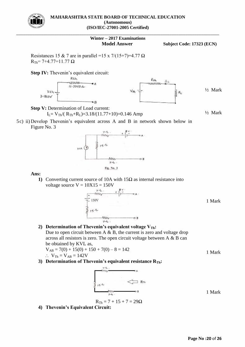
Resistances 15 & 7 are in parallel =15 x 7/(15+7)=4.77 Ω
RTh= 7+4.77=11.77 Ω
Step IV: Thevenin’s equivalent circuit:
Step V: Determination of Load current:
IL= VTh/( RTh+RL)=3.18/(11.77+10)=0.146 Amp
½ Mark
½ Mark
5 c) ii) Develop Thevenin’s equivalent across A and B in network shown below in
Figure No. 3
Ans:
1) Converting current source of 10A with 15Ω as internal resistance into
voltage source V = 10X15 = 150V
2) Determination of Thevenin’s equivalent voltage VTh:
Due to open circuit between A & B, the current is zero and voltage drop
across all resistors is zero. The open circuit voltage between A & B can
be obtained by KVL as,
VAB = 7(0) + 15(0) + 150 + 7(0) – 8 = 142
VTh = VAB = 142V
3) Determination of Thevenin’s equivalent resistance RTh:
RTh = 7 + 15 + 7 = 29Ω
4) Thevenin’s Equivalent Circuit:
1 Mark
1 Mark
1 Mark

MAHARASHTRA STATE BOARD OF TECHNICAL EDUCATION
(Autonomous)
(ISO/IEC-27001-2005 Certified) __________________________________________________________________________________________
Winter – 2017 Examinations
Model Answer Subject Code: 17323 (ECN)
Page No :21 of 26
1 Mark
6 Attempt any FOUR of the following 16
6 a) Calculate current through 10Ω resistance in the network shown in Figure No. 4
using superposition theorem.
Ans:
A) Consider 5 V source only:
.
Resistances of 10 & 20 are in parallel = 10 x20/(10+20) = 6.667Ω
Total current I= 5/(8+6.667)=5/14.667 =0.341 amp
Therefore I’=0.341 × 20/(10+20) = 0.227 amp
I’ = 0.227 amp from B to A
B) Now consider 7 V source only:
Resistances of 10 & 8 are in parallel=10 × 8/(10+8) = 4.44Ω
1 Mark
1 Mark

MAHARASHTRA STATE BOARD OF TECHNICAL EDUCATION
(Autonomous)
(ISO/IEC-27001-2005 Certified) __________________________________________________________________________________________
Winter – 2017 Examinations
Model Answer Subject Code: 17323 (ECN)
Page No :22 of 26
Therefore current I =7/(20+4.44) = 0.286 amp
I” = 0.286 × 8/(10+8) = 0.127 amp from A to B
C) Final Current:
I = I’ - I” from B to A OR I = I” - I’ from A to B
= 0.227 - 0.127 = 0.099 amp from B to A
1 Mark
1 Mark
6 b) Using Norton’s theorem, find current through 4Ω resistance in Figure No. 5
Ans:
Here load branch is 4Ω, hence RL = 4Ω
A) Determination of Norton’s Equivalent Current Source IN:
Remove RL and short the path, now circuit becomes as shown below
Apply Superposition theorem to find out the ISC = IN
(i) Consider 10 V source only
ISC’ = 10/(6+3) =10/9 = 1.11 amp from A to B
1Mark

MAHARASHTRA STATE BOARD OF TECHNICAL EDUCATION
(Autonomous)
(ISO/IEC-27001-2005 Certified) __________________________________________________________________________________________
Winter – 2017 Examinations
Model Answer Subject Code: 17323 (ECN)
Page No :23 of 26
(ii) Consider 6 A source only
ISC” = 6 amp from A to B
ISC = IN = ISC’ + ISC” = 1.11 + 6
IN = ISC = 7.11 amp from A to B
B) Determination of Norton’s Equivalent Resistance RN:
Now calculate RN = RTh
RN = RAB = 6+3 = 9 Ω
Norton’s equivalent circuit becomes
Therefore current through RL is IL= 7.11 x 9/(9+4)
IL = 4.922 amp
1 Mark
1Mark
1Mark
6 c) Find current through 8Ω resistance using nodal analysis in Figure No. 6.
Ans:
1 Mark

MAHARASHTRA STATE BOARD OF TECHNICAL EDUCATION
(Autonomous)
(ISO/IEC-27001-2005 Certified) __________________________________________________________________________________________
Winter – 2017 Examinations
Model Answer Subject Code: 17323 (ECN)
Page No :24 of 26
By applying KCL to Node A
I1+I2+I3=0
Current flowing through resistance 8 Ω =
1 Mark
1 Mark
1 Mark
6 d) Find the value of RL to transfer maximum power in the network shown in Figure
No. 7
Ans:
Maximum power will be transferred when load resistance is equal to internal
resistance i.e. RL= RTH
Resistances of 6 & 4 are in parallel = 6×4/(6+4)= 2.4 Ω and circuit is simplified
as
RTH=2.4+8= 10.4 Ω
Hence in the given circuit maximum power will be transferred when
RL= Rth=10.4Ω
1 Mark
1 Mark
1 Mark
1 Mark

MAHARASHTRA STATE BOARD OF TECHNICAL EDUCATION
(Autonomous)
(ISO/IEC-27001-2005 Certified) __________________________________________________________________________________________
Winter – 2017 Examinations
Model Answer Subject Code: 17323 (ECN)
Page No :25 of 26
6 e) Explain concept of initial and final conditions in switching circuits. For the
elements R, L and C.
Ans:
Concept of initial and final conditions:
For the three basic circuit elements the initial and final conditions are used in
following way:
i) Resistor:
At any time it acts like resistor only, with no change in condition.
ii) Inductor:
The current through an inductor cannot change instantly. If the inductor
current is zero just before switching, then whatever may be the applied
voltage, just after switching the inductor current will remain zero. i.e the
inductor must be acting as open-circuit at instant t = 0. If the inductor current
is I0 before switching, then just after switching the inductor current will remain
same as I0, and having stored energy hence it is represented by a current
source of value I0 in parallel with open circuit.
As time passes the inductor current slowly rises and finally it becomes
constant. Therefore the voltage across the inductor falls to zero*
+. The presence of current with zero voltage exhibits short circuit condition.
Therefore, under steady-state constant current condition, the inductor is
represented by a short circuit. If the initial inductor current is non-zero I0,
making it as energy source, then finally inductor is represented by current
source I0 in parallel with a short circuit.
iii) Capacitor:
The voltage across capacitor cannot change instantly. If the capacitor voltage
is zero initially just before switching, then whatever may be the current
flowing, just after switching the capacitor voltage will remain zero. i.e the
capacitor must be acting as short-circuit at instant t = 0. If capacitor is
previously charged to some voltage V0, then also after switching at t = 0, the
voltage across capacitor remains same V0. Since the energy is stored in the
capacitor, it is represented by a voltage source V0 in series with short-circuit.
As time passes the capacitor voltage slowly rises and finally it becomes
constant. Therefore the current through the capacitor falls to zero*
+. The presence of voltage with zero current exhibits open circuit
condition. Therefore, under steady-state constant voltage condition, the
capacitor is represented by a open circuit. If the initial capacitor voltage is
non-zero V0, making it as energy source, then finally capacitor is represented
by voltage source V0 in series with an open-circuit.
The initial and final conditions are summarized in following table:
Element and condition
at
t = 0-
Initial Condition at
t = 0+
Final Condition at
t =
1 Mark
1 Mark
1 Mark
1 Mark
For table

MAHARASHTRA STATE BOARD OF TECHNICAL EDUCATION
(Autonomous)
(ISO/IEC-27001-2005 Certified) __________________________________________________________________________________________
Winter – 2017 Examinations
Model Answer Subject Code: 17323 (ECN)
Page No :26 of 26
6 f) Give the expression for star to delta and delta to star transformation.
Ans:
Star to Delta Transformation:
Delta to Star Transformation:
1 Mark
½ Mark for
each equation
= 1½ Marks
½ Mark for
each equation
= 1½ Marks