manual: pc20n sm fimi en - archive.org
TRANSCRIPT

SERVICE MANUAL
HIGH RESOLUTION GRAPHICS MONITOR
FC 16N/FC 20N

Technical Operations Manual
_ Philips High Resolution Graphics Monitors
Models C16-N and C20-N- |

Table of Contents
Part I: Monitor Operations
1 Mo mitor Overview ......cccccscssssssssserecosecsncesscsesssssnssensnsonsosessonenes Besa tietsesied
1.1 Block Diagram... Wisdicaeddccstaavacstavsculesseoeseeemsess: a peactenticess oes emia 1-1
1.2 Monitor Specifications ...........-ccrer sessoncassseqnensenconsneasossnsscsnconenesagees 1-3
2 Power Supply & Degauss Circuitry savccevesssscssecccccensossssscccccesonaseseesesoneeees 2-1
2.1 Power Supply .........ccsssssccseesssssonssersrseerses es tissaia saeuuiswabedavineseayyeedoneets 2-1
2.2 CHOPPED -sscccccceseesconsnnnessssssnanannnnansnnnnnnnnrenscncegcnnenonnnereneeresessenennsssstet%4 2-3
9 Degaussing CUrCUIt ...eccccoccccccscseccersncesersscsescessassnscoscsenseensorsees veteussocees 2-6
3 Deflection Board . vceencavsccssccscesevsocssensocassnsonasssnsoocessssseseesseessenesessesencessseneee
3.1 Horizontal Deflection icant int peal sui ss seu a bade asguscuuabonaaausssaunteocees’s
3.2 ERT Stabilization Circutit ........ssssssscseeseresessesrsnenerersnessensncsees Pere
3.3 Vertical Deflection .............ssssssscescrssreesnecers sisi ahealidedelgauaaeusesseuaiiess
3.4 Arrxiliary Services .....cccssssssssseserssensasnnsssesceenenens Ss ucto cages eens scenes
4 Video Preamplifier Board .. sensccccceccsecsesoncccuccssossnscooocaccossasasceessseen sees
4.1 Video Preamplifiers........sussscvssessesersseee ee ee eee
4.2 Synchronization ........cssscosersseseessssssneereeersseesnnsenscnssenenssnscenssessenseesseste
5 Video Output Stages (Socket Board) .....-..sssccervessesrnsensnsessesensensereesoore
5.1 Fimal Video Stage ..........sssscsrsssssssssessnsssenssessenssonssensenenegsacessaresernsnnss
5.2 Black Level Adjustment and Individual Beam Limiting dacetsanss
5.3 Flashover Protection .......-..sssssssssssssernsssseresvsesrasecensenonassssnrecnnssernnse
6 Dynamic Focus Board .....-..ssvsosssssvsssnseenrennsssesseconneenssnnsonsennsensrensennesees ene
Part II: Adjustment Procedures
7 Equipment Needed for Adjustments .....ccccssrssssnesvcescessencnncassensencsnencenees
8 Synchronization . -oonssenassosccsrenseocssconcsocsssscnsssoooccocsroosnsssesssseessseeeeeesesecese eee
9 EHT Stabilization re
wl 3-1 3-3 3-4 3-4 4-1 4-1 4-2
5-1 5-1 5-1 5-1
6-1
10 Geometry —___cocsommeumesadeneees entnnuenssssssensunssssesesersssssansnsscsensnsesennenssscsensnssnoeee LOSE
11 Chromaticity ... shih sccipseetdte alec enete cea ncae aca cae caceea nate seed 11-1
| 12 FOCUS ..cccccccrcrorecece aches eae estates 12-1
13 Troubleshooting ..........-cscecsssscsssssecescereenenssssscsenssseenensseseseseansononseseseneerees 13-1
13.1 OVEIVIEW ..ccccceccesesnccsnscccencccsssencsersscscscareseseesenrs ones weeds Dspace oaetes 13-1
13.2 Indicators ....sssssrseseceeemerseesnreeernrees sosssscneesonnnenececenngnnceceecenennnscenmantt 13-1
Appendix A: Monitor or iestancaseessorecs Se ae camera scat eaeaaeaeee
——— B: Layout Dingeatnge tee Sees wesegaseues

Preface
This Technical Operations Manual is divided into three major parts:
e PartI- Monitor Operations
e Part Il - Adjustment Procedures
e Appendix
Part I, Chapters 1-6, describes the major components of the monitor, includ-
ing a monitor overview and circuit descriptions for each of the major com-
ponent blocks. |
Part II, Chapters 7-13, provides instructions for adjusting the monitor’s con-
trols and includes a chapter on troubleshooting.
Appendix A presents a series of diagrams describing monitor dimensions, —
control locations, and how to access and replace monitor component boards.
= B contains layout diagrams for the monitor’s five component
oards.
Inserted in the back of the manual is a monitor circuit diagram which is
referenced throughout the document. |

Table of Figures
Monitor Block Diagram ..........ccscsscsssssesscsessessesecssssesessecessesereesereseess 1-2 Power Supply & Degauss Circuitry Block Diagram ............0.-0s. 2-2 Chopper Block Diagram ..............0.. I scestooecsecaleeicet hoes icessscabnssenscadeuss 2-4 Deflection Board Circuit Diagram ........scccsscsssssscsosssssessesecesssseess 2-5 ENT Stabilization Circuit Diagram ..........cscsccecsscsscesseseccesssesecerseees 3-3 Dynamic Focus Board Circuit Diagram .0.....-essssccsccceessecsessessseene O° 1
Appendix A: Monitor Diagrams
A-1 A-2 A-3 A-4 A-5 A-6 A-7 A-8 A-9 A-10 A-11 A-12
Appendix B: Layout Diagrams
Monitor Mechanical Dimensions C16-N ......c.ssssssssscessssececssucceeess A-1 Monitor Mechanical Dimensions C20-N .u.....tescsssesssscesescceccscseeaee A-2 Removing the Pedestal C16-N .....csssssessscssssssscssssssscescesesasesassesecsess A-3 Removing the Back Cover C16-N ....cssssssssssssrsssessssetsesececesneseters A-4 Removing the Back Cover C20-N u..ccessscsscsscssescsssnscescesascesecsesesacees A-5
- Removing the Top Metal Cover C16-N & C20-N ..........000. sieaueeO Top Accessible Controls C16-N & C20-N wuccceccsescsccssecsssssssesesseeee A-7 Side and Back Controls C16-N & C20-N uu. .eessssscessesesecscsssesceess A-8 Replacing the Power Supply C16-N & C20-N ooeceecescsesssesceseeces A-9 Replacing the Video Preamplifier Board C16-N & C20-N ....A-10 Replacing the CRT Socket Board C16-N & C20-N .u..ecesesssseene A-11 Replacing the Deflection Board C16-N & C20-N ...cecccceseseseees A-12
Power Supply Chopper Board Deflection Board Video Preamplifier Board Socket Board |
Insert: Monitor Circuit Diagram

1 Monitor Overview
The C16-N and C20-N are high resolution color monitors specifically — _ designed for CAD/CAM applications to display graphic and alphanumeric information with a resolution of up to 1280 x 1024 pixels. The monitors are in a plastic cabinet with a tilt/swivel base.
1.1 Block Diagram
The block diagram of the monitor is shown in Figure 1-1.
The electronic circuits are divided among the following blocks:
e: POWER SUPPLY and DEGAUSS CIRCUITRY e DEFLECTION BOARD e VIDEO PREAMPLIFIER BOARD e CRT SOCKET BOARD e DYNAMIC FOCUS BOARD (only for C20-N)
Each of the blocks are described in Chapters 2 through Chapter 6.
il

: POWER MAINS | SUPPLY
CONTRO DYNAM ot BOARDS gee
{ONLY FOR C20)
Figure 1-1. Monitor Block Diagram
42 4 | , | |

1.2 Monitor Specifications
‘Refer to Appendix A for dimensional diagrams for the C16-N and C20-N
monitors.
1.2.1 Picture Tube
M48KDB56 X 40 (20") M38JFJ37 X 31 (16")
© 16" and 20" high resolution color tube coil assembly
90° deflection angle
0.28 (16") and 0.31 (20") trio dot pitch
29 mm neck diameter |
P22 phosphor, medium-short persistance
CIE chromaticity coordinates: X;=0.618 Xg=0.280 Xp =0.152
Yr=0.350 Yg=0.605 Yb = 0.063
white coordinates: X=0.281 +/- 0.02
Y =0.311 +/- 0.02
White coordinates are measured at the center of the CRT face on a white
window equal to 25% of total picture. |
The contrast control is set to 30 FL. *
The brightness control is set to the threshold of raster extinction.
e Brightness
1. Normal intensity mode: 30-35 FL at 0.7Vpp video input signal.
Brightness is measured at the center of the CRT face on a white window
equal to 25% of total picture with the contrast control set to maximum
and brightness control set to the threshold of raster extinction.
2. Uniformity: Maximum variation from center to edge is <or = 40%
(monotonic). Brightness is measured on a full white page with brightness
control set to the threshold of raster extinction and the contrast control set
at 20 FL at the screen’s center. | |
-Misconvergence: 0.15 in the center 5
0.35mm within a circle diameter equal to the image height
0.45mm in the corners |
Color purity: No color impurity for each of the R,G,B colors
1-3

1-4
1.2.2 Deflection
Horizontal
Frequency range: 48 to 64 kHz Blanking time: > 3.5 usec Retrace time: 2.8 usec
Vertical
Frequency range: 50 to 120 Hz Blanking time: 39 lines — Retrace time: 550 usec
Synchronization
Composite sync on green (0.3Vpp) 75 ohm input impedance
Geometry
With nominal video inputs pincushion barrel trapezium shall fall within a 3mm band formed by two concentric rectangles.
Linearity
Difference between displayed character sizes: a. worst case - Ey= 10% b. between adjacent characters - Ey=5%
[ Ey = (max size - min size / max size) x 100] _
Jitter, hum: not visible
1.23 Video
RGB inputs: 75 ohm, analog with sync on green
amplitudes:
video pulse: min 0.65V - max 0.75V - typical 0.7V sync pulse: min 0.27V- max 0.33V - typical 0.3V
Resolution: up to 1280 x 1024
Bandwidth: 110 MHz (at -3dB) linear
Rise and fall times: < or = 5 nsec
- Overshoot: max 8%

1.2.4 Power Supply
e AC input Range A 92-132V
Range B 184-264V Range select accessible by the user
e Mains frequency: 47/63 Hz
e Switching frequency: 43 Hz +/- 2 Hz
@ In-rush current limitation: 50A/2 usec
e Max. consumption: 120W
1.2.5 Controls
e External:
Brightness, Contrast, Manual Degauss, and Power On/Off
e Internal: |
H-PH: _V-Hold: © Height: V-Cent: S-Pin: V-Lin: Width: H-Lin: H-Cent: Serv: Trap:
1.2.6 Input Connectors
Horizontal Phase Vertical Frequency Vertical Size Vertical Shift East/West Pincushion Vertical Linearity Horizontal Size , - Horizontal Linearity Horizontal Shift Service Switch (collapsing Vertical Deflection) Trapezoidal Corrections -
¢ Signals: BNC (75 ohm)
* AC power: CEE 22-6A
1.2.7 Safety
e UL, CSA, DHHS, VDE, PTB, TUV approved
1.2.8 EMI/RFI
° VDE0871/6.78 class B approved |
FCC-15J class B (approved on Philips system)
1-5

1.2.9 Reliability
s MTBF: more than 25,000 hours (
25°C | 7
including CRT) as per MIL-HDBK 217D at
1.2.10 Environmental Conditions
e Operating ambient temperature: 0°C to +40°C
e Storage temperature: -40°C to +65°C
Humidity: 5% to 90% RH (non-condensing)
1-6

2 Power Supply and Degaussing Circuitry
This chapter describes the circuitry of the Power Supply and the Degauss Coil. Figure 2-1 presents a simplified block diagram of these components.
2.1 Power Supply
— power supply works at a fixed frequency of about 43 KHz in flyback mode. |
The mains voltage, rectified (R1) and filtered (F1), is applied to the power —
transformer (T1) which, by the switching power transistor (Q1), transfers the
voltages and the energy necessary for proper operation to the secondary side.
The mains voltage range is selected by an external voltage selector slide
switch. In the 110V range, the bridge rectifier acts as a doubler circuit, and
in the 220V range, the bridge rectifier acts as a normal rectifier circuit.
An auxiliary voltage (Vaux) is also obtained from the primary side of the
transformer which supplies the Pulse Width Modulator (PWM) circuits
(based on the TDA 1060 IC), the driver stage, and the automatic-manual
degaussing circuitry. During startup of the power supply, the auxiliary volt-
age is not present, and the voltage necessary for the PWM is derived directly
from the rectified mains. |
The startup time is determined by an R-C network; the power supply can
only be restarted after the R-C network has been discharged.
On the secondary side of the power transformer, the square waveforms are
rectified and filtered (RF2, RF3), providing the following output voltages:
+64.5 V, +30V, +14.5V and +6V. ——
The +64.5V output is sensed and subtracted from a stabilized reference
voltage. The error signal is amplified and sent to the PWM circuit via an
opto-coupler, where it is compared to a triangular waveform at fixed fre-
quency. The resulting square waveform modulates the duty cycle in propor-
tion to the error signal in order to keep the output voltage constant at
+ 64.5V against mains voltage and load variations.
_ This square waveform is then amplified by the driver stage (transistor Q2 and driver transformer T2) and is applied to the power transistor T1, thereby
closing the feedback loop. | |
There are two protection thresholds. The primary current is sensed by resis-
tor RS. If the first protection threshold is exceeded, the duty cycle is con-
tained (thus limiting the output power). If the current increases even further
and surpasses the second threshold, the power supply is switched off.
If the higher output voltages (+64.5V and +30V) are short-circuited, the
primary current increases causing the power supply to be switched off.

sae (ake AULINDYTO
ONISSNV930
WANVH
9
| T
JTAVWOLNY
||
HOLV
IOSTOLd0
>
NOLINGHSNAd ONISSNV930
—WONVH
(OS0T VOL)
SJIYLINIUID
WMd
>.
S109
INISSNV930
0193735
$91d/39VIIOA WANtW3EXD
Figure 2-1. Power Supply and Degauss Circuitry Block Diagram
2-2

If the lower output voltages (+ 14.5 V and + 6V) are short-circuited, the primary current does not reach the turn-off threshold due to the lower power; for this reason, these outputs are short-circuit protected by a fuse. (An LED after the fuse indicates if the voltage is available on the output.)
In series with the +6V output, the resistor produces negative current feed- back in order to limit current variation.
An OVP circuit in the classic crowbar configuration senses the 30V and + 14.5V output voltages. The +30V output voltage is short-circuited by an SCR whenever the sensed voltage exceeds + 17.5V.
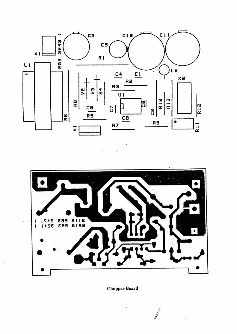
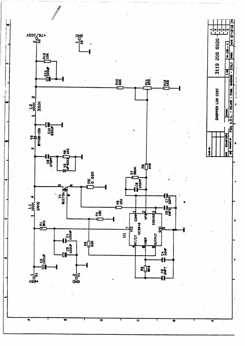
2.2 Chopper
Figure 2-2 presents a simplified chopper block diagram, and Figure 2-3 is a circuit diagram of the chopper.
A chopper circuit is mounted on the power supply and provides an output voltage which can be adjusted by a multi-turn trimmer from 76.5V to 102V. The horizontal deflection stage needs an input voltage proportional to the line frequency. In this way, a single power supply unit can be used for the whole family of monitors from 48 to 64 KHz.
The chopper contains a boost switching regulator working at a fixed frequen- cy of about 75KHz, a power inductor L, a power mosfet Q, a rectifier diode D, an output filter F, anda PWM. The +64.5Vdc input voltage comes from the power supply.
When the mosfet is turned on, the input voltage is applied across the power inductor, which stores the energy.
When the mosfet is turned off, the energy stored in the inductor creates a voltage which switches on the diode and transfers the energy to the output filter and then to the load. Additional energy is also transferred from the input directly to the output during the diode conduction time.
The +64.5V input voltage is applied to the PWM circuitry (based on IC | UC3842) via the resistor R.
The output voltage is sensed and is sent to the PWM where it is subtracted from a stabilized reference voltage.
The duty cycle of the PWM square waveform is modulated in porportion to the error signal and current amplitude in order to keep the output voltage constant against input voltage and load variations.
This square waveform drives the power mosfet, thus closing the feedback loop. When a short circuit occurs at the output, the input supply voltage is overloaded and the power supply is switched off.

24 | |
14 []*
ty |
id i
ACOUt+/AG
‘SL+
(2PBEON)
AYLINOYID
WMd
AG ‘bSt
Figure 2-2. Chopper Block Diagram
2-4

AzOt/9Le ex ar
youl dee
G4nt 43
99
4d008
¥O9S
Tt
63
ant ety
; /
ent
ong
i
—
1)
| 6u
3°
|
coud
Q
z=
rs)
font
. suas
W890
YY
. Su
fee
oY
4 5
yze
|,
ofu
5
e
" ons
coor
VEL2NG
ey
au
2A
:
| t
CT
|
fx
et
“,
-dd0LP
69
snoot
anoze
so
'T
O39
fF
0S3
-92AAG
t
HNEE
ur
el
t7
2.3 Degaussing Circuit
The automatic and manual degaussing circuitry supplies current (via the
PTC) to the degaussing coils mounted on the CRT for about ten seconds.
The cutrent supply is limited to ten seconds in order to allow the PTC to
cool off again and to remove the small residual demagnetizing current which
could affect spot landing. After approximately five minutes, the external
manual degaussing controls can be used again.
The degaussing circuitry consists of an R-C network, a comparator, an opto-
coupled triac driver and a triac, which connects the selected PTC to the
mains.
The R-C circuit determines the on-time of the triac.
Upon startup, the comparator drives the triac via the opto-coupler. When
the R-C network reaches its trip point, the comparator inhibits the opto-
coupler from driving the triac. | |
If the PTC is cold, the unit can be degaussed by simply discharging the R-C
network with an external pushbutton. |

3 Deflection Board
The deflection board contains the following circuits:
e Horizontal Deflection with EHT Generation
e ENT Stabilization Circuit
e Vertical Deflection
Refer to the Monitor Circuit Diagram included with this manual.
3.1 Horizontal Deflection
3.1.1 Horizontal Driver And Output Stage
The horizontal or composite synchronization signal coming from the video
preamplifier board is applied to pin 11 of IC Ul (TDA 2595/V7).
The local horizontal oscillator in IC U1 is locked by the input synchroniza-
tion signal. There are two phase loops.
The first phase loop compares the phase between the synchronization pulse
and the oscillator. The range of this phase comparator is limited in order to
prevent damage to the deflection circuitry at synchronization frequencies
beyond the acceptable range. |
The second phase loop compares the phase between the oscillator and the
horizontal flyback pulse which is derived from pin 7 of the line output trans-
former and applied to pin 2 of the IC U1. This loop compensates for storage
time variations in the horizontal deflection transistor VS. |
Resistor R13 will pull pin 4 of U1 high when transistor V4 does not conduct.
When driver transistor V4 conducts, a primary current will flow through the
driver transformer T1. 3 |
The secondary winding on this transformer supplies a negative base current
to the output transistor, V5. The base storage charge is first removed by this
negative current, after which, the output transistor actually ceases to con-
duct. The slope of this negative current is determined by the leakage induc-
tance of the driver transformer and the negative drive voltage, which 1s the
sum of the transformer drive voltage and the voltage across the base
capacitor C24. After the storage time, the base emitter voltage is driven into
negative breakdown. During this time, called the zenering time, the collec-
tor and the base current decrease to zero and turn-off is complete.
As soon as pin 4 of U1 is pulled low, the base voltage of V4 will fall below
the emitter voltage and V4 will be switched off. When the primary current
in T1 is interrupted, the magnetizing current in the secondary winding ap-
pears as an almost constant positive base current and V5 is turned on. |

R21 prevents undesired conduction of V5 caused by ringing in the driver stage. C17 is a speed-up capacitor.
ae V4 collector peak voltage is limited by the damping network R18 and ©
18.
The supply voltage for the horizontal scan is derived from the power supply
and is connected to the line output transformer T5 at pin 6.
3.1.2 Diode Modulator
| The diode modulator has two functions:
e horizontal amplitude adjustment
e east/west pincushion and keystone correction
3.1.2.1 Horizontal Amplitude Adjustment |
Since the average voltage across a coil has to be OV, the sum of the voltages across C29 (S-correction capacitor) and C32 (modulator filter capacitor) has to be equal to the supply voltage. | |
The width adjustment, pincushion and keystone correction circuits vary the voltage across C32, which in turn causes an identical and inverted variation
on C29, equivalent to the scan voltage for the horizontal deflection coil.
This means that a DC variation on C24 will result in a different supply volt- age for the horizontal deflection coils and therefore will affect the horizontal
amplitude. |
The advantage of this type of modulator is that the EHT is independent of the horizontal amplitude. |
3.1.2.2 East/West Pincushion Correction
The east/west pincushion correction is needed to obtain straight left and right sides of the picture. The required shape of this correction signal is a
parabola which is created by integrating the vertical sawtooth signal (as avail-
able on resistors R92-R93--see vertical deflection stage, Section 3.3).
The sawtooth voltage is applied to a circuit built around a QUAD OP-AMP (U3 - LM324) which generates the waveforms for east/west pincushion (R110) and keystone correction (R123); these waveforms are then applied
_ via the power transistor V51 to C32 for proper horizontal correction. -
This signal is sent to capacitor C32 which is the same capacitor to which the
amplitude DC-voltage is applied. In this way, a parabola-shaped deflection
current waveform is obtained without modulating the EHT.

3.2 EHT Stabilization Circuit
Because of the internal impedance of the EHT transformer, the size of the
displayed picture varies with brightness. For good picture stability, as re- —
quired Z a high resolution monitor, an EHT stabilization circuit is incor-
porate |
A block diagram of the EHT Stabilization circuit is shown in Figure 3-1.
An error amplifier compares a fraction of the EHT voltage, derived from a
voltage divider (bleeder resistor inside EHT transformer) with an adjustable
reference voltage (R52) and generates a variable supply voltage for the
power stage. ,
The power stage is a resonant flyback converter (V19, V21, C36, T4) which
generates a correction voltage between 0 and 2.000 Vdc which in turn is ap-
plied to the bottom of the EHT winding. |
| _lP9 ERROR |
] i 7 AMPLIFIER POWER STAGE
oy | REFERENCE NOG TREE VOLTAGE
CORRECTION VOLTAGE
Figure 3-1. EHT Stabilization Circuit Diagram
3-3

3.3 Vertical Deflection
The key component for the vertical deflection is IC U2 (TDA 2653A).
The oscillator is synchronized on pin 2 with a positive sync pulse coming
_ from the sync separator. The free running frequency of the oscillator can be
adjusted with potentiometer R67. |
The actual vertical ramp is generated by an external RC network on pin 11.
_ Resistor R69 charges C41 and C42 from the 30V rail.
During blanking, the capacitors are fully discharged by an internal transistor.
The sawtooth ramp is internally buffered and appears on pin 3. At the begin- |
ning of scan, this signal is almost 0V.
Without negative bias current, the initial part of the sawtooth would be
slightly distorted. To prevent this distortion, pin 3 is connected to a negative
bias voltage via resistor R64.
During flyback, the supply voltage (pin 5) is doubled by a pulse lifter (pin 7). As soon as the inputs to the error amplifier (pin 4 and pin 10) become equal, —
the pulse lifter is deactivated and the scan will start. |
The vertical deflection coils are driven by an AC-coupled current amplifier.
The linearity of the vertical deflection can be adjusted with R82.
The vertical amplitude can be adjusted with R89.
Vertical centering of the raster is obtained with R101, adding an adjustable
DC current to the vertical deflection current. |
3.4 Auxiliary Services
3.4.1 Grid 1 Circuitry and Beam Current Limiter
The function of beam current limiter (BCL) is accomplished by transistor
V26. Normally, V26 is bottomed.
As soon as the EHT current exceeds the total current flowing through R55,
V26 comes out of bottoming and its collector goes negative.
This voltage is sent to the remaining part of the BCL circuit located on the
video preamaplifier board where it is buffered by V511.
Via diode V512, normally non-conducting, this voltage pulls Vel instantly to
a more negative voltage when the picture is too bright. |
3-4

R55 is calculated to give a maximum average beam current of 600 uA at max-
imum video signal.
3.4.2 Deflection guard circuit
The purpose of the deflection guard circuit is to prevent spot burn of the
CRT if the monitor is switched off or if the deflection fails.
A three transistor circuit monitors both the horizontal and the vertical
deflection.
A 1nF capacitor (C39) is charged during scan and discharged by the presence of proper horizontal flyback pulses. As long as the resulting saw- tooth does not exceed the 6.2V of a zener diode, no action is taken. ,
The vertical guard is identical, except that the value of capacitor C40 is 1luF.
If either deflection ceases, the collector of V41 goes low on the next scan and will cause the grid 1 drive on the video board to become very negative. This cuts off the picture completely, overruling the actual video drive on the
cathodes. :
3.4.3 X-ray Protection
IC U1, R11, and associated components around the horizontal oscillator
form the X-ray protection circuitry. |
The flyback voltage from pin 4 of the line output transformer is rectified and filtered by V3, C15, and C16. : | 2
Part of this voltage is applied to pin 8 of U1, and when it exceeds a certain level, U1 is blocked, switching off the monitor.
The trip threshold is regulated by R11 in such a way that under no cir- cumstances can the EHT exceed 29 KV.


4 Video Preamplifier Board
Refer to the Monitor Circuit Diagram included with this manual.
?
4.1 Video Preamplifiers
The three video preamplifiers are located on the Video Preamplifer Board together with sync separator and grid 1 circuitry. :
The video input signal for each amplifier coming from an external BNC con- nector is terminated by a 75 ohm resistor.
The nominal input amplitude is 0.7 Vpp for the red and blue. The green sig- nal has an amplitude of 1 Vpp which includes 0.7 Vpp for the video and 0.3 Vpp for the composite sync.
The description will be given only for the red amplifier since the other two are identical. _ |
Component numbers in brackets refer to green and blue channels.
The signal enters the differential input section of the video preamplifier U401 (U431, U461) MC 1496 on pin 4.
The second part of the MC 1496, together with the dual transistor U503 (LM394) forms a four quadrant multiplier (known as a Gilbert cell). One LM 394 is used for all the three channels. |
This configuration is very suitable for obtaining the individual gain setting for both the color balance adjustment potentiometer R403 (R433, R463) and the cold contrast control (potentiometer R800, transistor V504) to achieve very good grey scale tracking.
The output amplifier consists of output transistors V404 and V405 used as a Darlington.
The output current of this stage is sent to the final stage located on the CRT socket board, explained in Chapter 5.
For optimum video performance, the video output signal (which is AC-_
coupled to the video amplifier) needs to be referenced to a fixed DC volt- age. This is achieved by an active black level clamp circuit, transistors V403,
| vaes} V407 and diode V408 (V433, V436, V437, V438 - V463, V466, V467, 468). |
This circuit is activated during the horizontal back porch time and controls the base bias voltage of V404 (V434, V464) by charging or discharging the coupling capacitor, keeping the black level at the desired value.

The grid 1 drive is a combination of four different functions:
1. Black Level Control (also called "brightness control")
Adjust the external potentiometer R801 to change the grid 1 voltage (nominal
cut off level -37V). It can therefore compensate for changes in the ambient light
levels, drift during warm-up and during life of the CRT.
. Blanking
A vertical pulse is superimposed on VG1 via capacitor C522. This suppresses
the retrace lines. 7
. Total Beam Current Limiter
The total beam current limiter information from the deflection board is buffered
by transistor .V511. If the picture becomes too bright, VG1 is pulled down to a
more negative level by via diode V512, which is normally non-conducting.
. Spot Protection |
As explained previously, the deflection guard circuit generates a protection sig-
nal that puils VG1 fully negative, thus blocking any light spot on the screen.
- This safety precaution will not only work at any deflection failure or power
switch-off, but also if the protection signal line itself becomes accidentally open-
circuited or grounded. | *
4.2 Synchronization
The aim of this circuit is to subtract the horizontal and vertical synchroniza-
tion pulses from the composite green video signal. |
The video signal is fed via a buffer stage V505 to the sync separator
V506/V50 where the composite sync is separated from the video. The com-
posite sync is then fed to the sync processor IC on the deflection board.

5 Video Output Stages (Socket Board) Refer to the Monitor Circuit Diagram included with this manual.
5.1 Final Video Stage
The final stage of the video amplifier is composed of transistor V602 (V612, V622) which is connected in common-base configuration. It converts the ~ current signal coming from the preamplifier into voltage signals sufficient to drive the cathodes of the CRT. | ;
5.2 Black Level Adjustment and Individual Beam Limiting
Because of spreads in cut-off levels among the three cathodes in any color CRT, the black level on each cathode must be adjustable over a range of about 20V to account for this differential cut-off spread.
For this purpose, a DC level shift is provided for each channel, allowing for cut-off adjustments and individual beam current limiting functions. The cir- cuit is built around V606 (V616, V626) and associated components. This cir- cuit keeps the coupling capacitor C603 (C613, C623) biased with an adjus- table DC voltage, thereby creating a DC shift in the video output signal without affecting the dynamic range of the final stage.
This circuit also acts as an individual beam current limiter: R608 (R618, R628) carries a constant current Ibeam, which is the sum of the beam cur- rent and the emitter current of V606 (V616, V626).
If the beam current should exceed Ilim, diode V607 (V617, V627) will open and the extra current will charge C603 (C613, C623), causing the video sig- nal to be shifted above the cut-off point and the beam current to be reduced.
5.3 Flashover Protection
The video amplifier is protected against flashover from the CRT electrodes by a neon lamp V609 (V619, V629) which acts as a spark gap between cathode and ground. |
A limiting network composed of resistor R609 (R619, R629) and diode V601 (V611, V621) prevents extra currents and voltages from reaching the video amplifier.

Flashover protections from other CRT electrodes (G1, G2 and heater) are
obtained by spark gaps in the form of cuts in the PCB.
G1 is further protected by V632, and G3 has a built-in discharger in the sock-
et. | | |
The passive components on the electrodes (R631, R633, C636, C637, C638, L631, L632, L633) are used for decoupling and filtering purposes.

6 Dynamic Focus Board (C20-N)
Figure 6-1 shows the Dynamic Focus Board circuitry. (This board is only used on the 20" monitor.) :
The C20-N series of monitors employs a new CRT with a special gun called DAF (Dynamic Astigmatic F on.
This new gun has two focusing electrodes; a dynamic correction voltage is ap- plied to one of the electrodes.
The dynamic correction voltage is the sum of line and field frequency
parabolas which are synchronized to the horizontal and vertical flyback pul-
Ses, -
Out To Crt Block
|
X —x508-
Figure 6-1. Dynamic Focus Board Circuit Diagram


Socket . Board

mn i | ard
; ( ' 7
w a Be 2 far > L- oo lo | a
= PoP Fw VM = a o E = = s[ ~ a 3 aa = = = ; |™ gC) a! 13 C636 S| |2la|q- C613 a =12 | s' |2/8/2 [jag PP P 1S wf | V615 3 = Gs ; —_ R616 [= oa mw
2 = _ 2 Cea7 — wo} om = v612 a pe <'> ww
me ~wJ
: V632 - a {= R613 a =.= = L612 | on
| X684 zs \ R617 Pr X685 a us = = ees
| ™ C615 se R688 Is
x | a a
ig SL] oss / (28 Ss 4 fad} PRES
Gn ~ a CO, R6aS | — 2
R627 ee 7 7 Cj & wm a” o V631 «a
— 229) eegu
TT 9 1e9u
te9 -{+— 129A 8e9u
8
Rm V6e2 _
| C626
Socket Board
€agu /
489u
a5


Video Preamplifier Board
8219 253 3168.3
€099 ie
Zt @) ose O1@)) a< (B) rs) oO QO : “~ ‘er 2 = si | © LOVA 907A EDTA Oo O74 oO
Esdehdag = 1S 2 107 ~l07VH o eI 7) x S| ee eo? Ce x es “z Siva ro) a oO =| 5 o 207A, | | toa = 6079) | = S = ©] wid 807A ~ © ~ Lo7g — a ed Re are | eo o Zi73 PS =) a} =} & < @2 S| Ziva |g 2073 (a SO7A 079 S074 z 3 + “S070 + bis, 9074 rT) | = 3079 L179 Oc. ae S LEVA SEYA EEXA eo 2E9M coe 5 73749 an ps |= EL7D m 3 IE o ZE7
zt PE ey s77a om 5 s| ~ EAL | teva —— 6€79; | 3 & x ol wl SETA mv LEVY nr wi ow ~~ <ZI9 CUS RS: a ~ 277) = S| 2] al o ol + wn oo TEVA 4 ——m pet
“5778 Sry 8975 x =| 5 9€79 L779 mi | © LOVA S9%A ESYA 2994 579 — Si [6 c97) Wee Ne |S _ =. 3 os or o ny «= 7D -|9 a - —e ik: Si >< > - S| x | ZO7A e874 BETH e595 ,%| © n $
ol wl 897A om 2 i994 = ro ol S © wis S :
w
oc 2 799A | Pm c som | 9955 ———o LL7a S979 so7vd yy St “F595 ee 6174 $97 L709 S| > 9979 sect ££79 cou NN __ SES fi7) 0S 0Sa—~CéC SS g0Su = 578s “7058 —«—« _90u 5 cOSA E0Sa = O |) |) 9782 sya ZOSu , = ©
LZSA _f&Sy__ ai 70 i) 2 rae ~_ 7s © zO0S2 re — SISA 9ES¥ leSy wn “Wert n| 2 = s 3 2 =a = ms) —tISd 5085 idss S g9€S9 2 ie > ~ 9758 = ater e759 BSH | | ajay +4228 S24 —19sa © Ni CC) TEP B A 8 “ssa 3 |) ° \ 7 7S mTx-t0 > oo > = pa eS) €SS) wm YT in cood ys ow ZES) 2 99Sa ce ~ ZS ZSA VP! wn as sl) > S59 2 SISA > tse, pea |B “ rae al = ee ax see OR at bs Al | alanis 2 3] Sista) 2 o| ~sse- ( )e 9555 x ~ OO" Be 2 | eiciel > é7Su VISA" 27Sy___s sSYSs—(‘iéiS Xe. e 2 \7Su eso > a5 | (Ys
aera — xcL_|< =) oo to 8 o zsy_ ss be = a a a


O fe) GS O
O O
Deflection Board
x
253 3243
INSPE EAS CLIle baSE E€eS e:S8
: AS Chopper Board


S PELE CSzZ GizE
Power Supply

7 Equipment Needed For Adjustments
The following equipment is necessary to perform the adjustments described in Chapters 8-12.
° Programmable pattern generator (Quantum 801C, Opix, Astro, etc.) or a
test pattern program from the host computer
_e Luminance meter
e Metric rule
e Screwdrivers of different sizes
e Degaussing tool
If you are using a programmable pattern generator, be sure you know the exact timing specification to which the monitor must be adjusted, and then set up the generator. (Follow the generator operating instructions.)
If you are using the host computer as a generator, you need a test pattern program.
The minimum set of patterns is as follows:
e crosshatch
e white page
e black page
e red, green, blue, and white central rectangles ~
Refer to the diagrams in Appendix A for instructions on accessing the monitor’s controls.
To access service controls, remove the plastic rear enclosure. (See the con- trol location shown in Figure A-3.)
To access cut-off, focus, screen, and dynamic focus (for C20-N) controls, you must also remove the top metal cover. (See Figure A-4.)
Note
Before you start making any adjustments, the monitor must be warmed up for at least 20 minutes. This ensures that all three electron guns are at a stable temperature which is especially critical when you perform chromaticity adjustments.
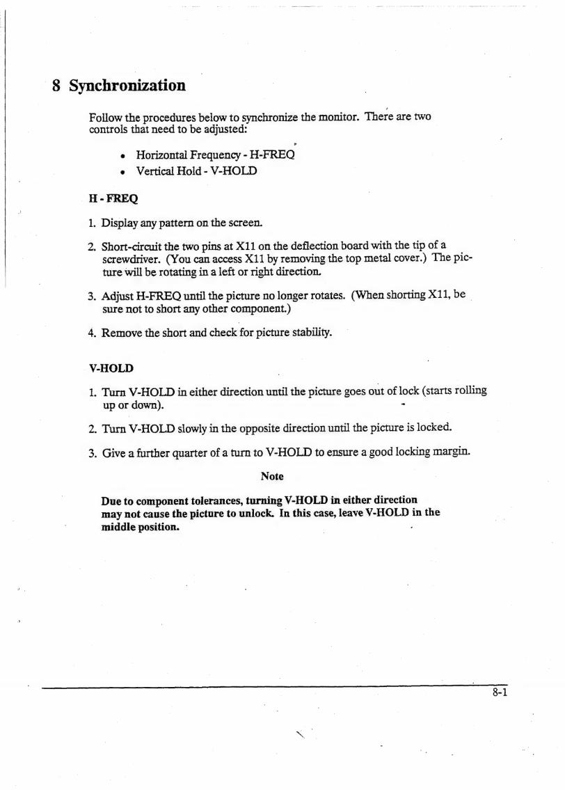
8 Synchronization
Follow the procedures below to synchronize the monitor. There are two controls that need to be adjusted:
e Horizontal Frequency - H-FREQ
e Vertical Hold - V-HOLD
H- FREQ
. Display any pattern on the screen.
. Short-circuit the two pins at X11 on the deflection board with the tip of a
screwdriver. (You can access X11 by removing the top metal cover.) The pic-
ture will be rotating in a left or right direction.
. Adjust H-FREO until the picture no longer rotates. (When shorting X11, be |
sure not to short any other component.)
. Remove the short and check for picture stability.
V-HOLD
L; Turn V-HOLD in either direction until the picture goes out of lock (starts rolling
up or down). -
. Turn V-HOLD slowly in the opposite direction until the picture is locked.
. Give a further quarter of a turn to V-HOLD to ensure a good locking margin.
Note
Due to component tolerances, turning V-HOLD in either direction
may not cause the picture to unlock. In this case, leave V-HOLD in the
middle position.

9 EHT Stabilization C16-N and C20-N monitors are provided with an EHT stabilization circuit for good picture stability. As the adjustment of this circuit affects picture
size, it must be performed before geometry adjustment.
Two adjustment procedures are described below. The first procedure is
more precise but needs an oscilloscope. The second procedure is simple but still produces good results. |
_ Procedure |
1.
2.
Display any pattern on the screen.
Reduce contrast, brightness and, if necessary, screen voltage until the screen is
completely dark.
. Connect the probe of the oscilloscope to the collector (tab) of V21 (BU806) on
the deflection board.
. Adjust the EHT stabilization resistor (R52) to read a peak to peak voltage of
about 30V on V21.
. Remove the probe.
. Put the monitor in normal brightness conditions (raster just visible).
. Display an all white pattern and check that the picture size does not change when
going from minimum to maximum contrast and brightness.
Procedure 2
1. Turn the EHT stabilization resistor (R52) fully counterclockwise.
bi
>.
Display a crosshatch.
Put brightness at minimum to completely blank the background raster. (If neces-
sary, reduce the screen voltage.) | | | |
. Reduce the contrast until you can just barely see the white lines. |
. Turn the EHT stabilization resistor until the picture size is reduced by about 3 ©
mm (1.5mm per side) on the 20" monitor, or 2 mm (1mm per side) on the 16"
monitor. | |
9-1

6. Set the monitor to normal brightness.
7. Display an all white pattern and check that the picture size doe
going from minimum to maximum contrast and brightness. s not change when

10 Geometry
This chapter describes the complete setting-up procedure, starting from an unadjusted monitor. If you have to perform only small readjustments, find the appropriate starting point in the procedure below.
Controls involved in the geometry adjustments are:
e width
° height
e e/w pincushion
e trapezium/keystone
e Horizontal phase (H. phase)
¢ Horizontal center (H. center) e Horizontal linearity (H. linearity)
e Vertical center (V. center)
e Vertical linearity (V. linearity)
Start putting all of these controls in the central position except for H. linearity, which should be positioned for minimum correction (maximum pic- ture width).
Now display a centering or a crosshatch pattern and adjust the controls fol- lowing this sequence: ©
1. Adjust H. phase to center the picture in the raster. ;
2. Adjust H. center and V. center so that the picture is centered in the bezel opening.
3. Adjust H. and V. linearity. If you are using a crosshatch, check that the boxes have
the same width and height all over the screen. If you are using a centering pat-
tern, check that the left and right halves have the same width, and check that the
top and bottom halves have the same height. |
Linearity adjustment affects picture centering, so now repeat step 2.
4. Adjust width and height to the required values. This will not affect the previous
adjustments. | : |
5. Adjust e/w pincushion until the left and right sides of the picture are perfectly straight. | |
6. Adjust trapezium/keystone until the left and right sides of the picture are parallel.
7. If necessary, readjust the picture width.
10-1

11 Chromaticity
In acolor CRT, white light is obtained by the addition of certain amounts of red, green, and blue light.
Chromaticity adjustment is necessary to align the emission of the three guns _ of acolor CRT to the desired level. The adjustment is performed in two steps: 7
1. Cut-off Adjustment
The purpose of this operation is to align the three guns to the same threshold of emission, so they start to emit electrons simultaneously.
A. Display a black page on the screen (i.e., only sync - no video). If you cannot
display a black page, turn the brightness to minimum and internal controls
for minimum light output (R,G,B cut-off CCW, R, G, B gain CW, C-lim
CCW). Switch off the monitor. | |
B. Turn the service switch on the deflection board to to its central position. (This
will collapse the vertical deflection without activating spot burn protection,
so a horizontal line can be displayed.) Turn the screen voltage control to
the minimum setting on the monitor (fully CCW), and let it warm up for
five minutes. | |
C. Increase the screen voltage slowly until you see a line across the screen.
Remember what color it is. Reduce the screen voltage untit the line disap-
pears. |
D. Repeat the above operation for the remaining two colors using the cor-
responding cut-off control, instead of screen voltage control.
E. Now increase the brightness slightly with the external control until you Just
see a white line across the screen. If the line is not white, repeat steps C and
D more carefully.
F. Switch off the monitor, turn the service switch to either the left or right posi-
tion, switch on again, and check for presence of the raster using the bright-
ness control.
11-1

11-2
2. Color Balance Adjustment
The purpose of this adjustment is to get the correct white color temperature on the screen.
To perform this adjustment, you need a luminance meter and a reference monitor (i.¢., a monitor which you are sure is perfectly adjusted) for calibration.
The calibration procedure is as follows:
A. Switch on the reference monitor and let it warm up for at least 20 minutes. Set the contrast control to maximum and the brightness control to the
threshold of extinction of background raster.
_ B.. Display red, green, and blue central rectangles; read and take note of the luminance for each of these patterns. _
C. Now you have the reference values you can use these to adjust any monitor. Keep these values together with your luminance meter; it is recommended that you check the calibration of the luminance meter every two or three weeks.
D. On the monitor, put R-gain, G-gain, and B-gain to the minimum setting (CW), contrast control to maximum, and brightness control to the threshold of extinction of background raster.
FE. Display a green central box and put green gain to maximum; measure the _ brightness and sesh it to the reference value for green using the C- lim con-
trol.
F, Display a red central box and adjust the brightness t to the reference value with R-gain. Repeat for blue. |
G. Display a white box and check that there is no color aiteration (i.e., reddish or bluish, etc.), turning the contrast control from minimum to maximum. If necessary, repeat the procedure.

12 Focus >
hie adjust the focus on your monitor, follow the appropriate proc
edure
elow. —
Non DAF Models _(C16-N)
1. Display a crosshatch or a screenful of characters.
2. Adjust focus for maximum picture sharpness.
DAF Models_(C€20-N)
To adjust the focus correctly, follow these steps:
1. Display a green crosshatch and adjust focus 2 for ma
ximum sharpness of the verti-
cal lines. (It will also affect the horizontal lines, but that does not
matter.)
2. Adjust focus 1 for maximum sharpness of the horizont
al lines. (It will not affect
the vertical lines.)
12-1
we IE
oo
ta ate
An
Ze +1
tae
ee mee
ere
teens
tt
Meswies
Meetnne
vbr
a
w
v
Ld
| 82-23-20
aive]
emo]
AAT
- ONNORVS
‘OaVd
- ONVIIN
= 1
up
tid
smoctwi
lofes
fre
|
eae
0c09
B0¢e
ETITE
. ee eee Pee
4S09
MO")
YaddOHD
‘ adze
[sant
AZ0T/SZ+
cule

13 Troubleshooting
13.1 Overview
When you encounter a problem but can still see a picture on the screen, the
problem usually involves control readjustment. If there was a Serious |
monitor failure, a protection circuit would blank the screen. —
Before changing any FRU, check to see if it is possible to solve the problem —
by readjusting the related controls.
13.2 Indicators
The monitor has built-in indicators which can help you to understand the
problem. When you do not see a picture, look at these indicators in the fol-
lowing order. Once you have determined that the indicator in question 1s
working properly, go on to the next indicator. |
1. Noise
If the monitor emits a crackling noise whether it is off or on, this means that
either the EHT has been applied to the anode of the CRT at power on, or that
the EHT is going down at power off. If you hear the noise at power on but not at
power off, it means that the X-ray protection on the deflection board has been
activated because the EHT has reached a dangerous level. The problem could
be a failure in the SMPS (output voltage too high) or in the deflection (e.g.,
monitor not synchronized and working at too low a frequency).
2. Front Panel LED
If on, it means that mains voltage is reaching the SMPS. It does not necessarily
mean that the SMPS is working properly.
If off, it means that mains voltage is not present. Possible causes and suggested
actions are: | .
Cause Action |
mains absent at AC outlet It is not a monitor problem.
bad power cord Replace power cord.
fuse blown | Replace the fuse. If it blows again,
replace the smps FRU.
ET
13-1

3, SMPS High Voltage Output LED
Tf on, it means that the regulated output voltage of the SMPS is present. It does
not necessarily mean that the SMPS is correctly adjusted. :
If off, either of the following is possible:
a. The SMPS protection has been activated because of a short circuit on the out-
put. In this case, disconnect the supply connectors from the other boards |
‘one at a time and switch the monitor on again. If the SMPS starts working,
the FRU which has been disconnected is bad. | |
b. The SMPS is bad.
4. SMPS Low Voltage LEDs
The 6V and 14.5V outputs of the SMPS have a series fuse. If one of the low volt- —
age LEDs is off but the high voltage one is on, it means that the SMPS is work-
ing correctly, but one fuse +s blown because of an overload or a short on the cor-
responding output. In this case, before changing the SMPS, you have to find the
bad FRU. The 6V line is only supplied to the socket board, while the 14.5 V is
sent to the deflection and socket boards.
5. Vertical Deflection LED
If on, it means that the vertical deflection is working. It does nét necessarily
mean that it is correctly adjusted.
If off, the vertical deflection is not working, the EHT is absent, the spot burn
protection is activated, and the screen is blanked. In this case, check the cabling
(especially the horizontal yoke connection); if all is correct, replace the deflec-
tion board. |
6. Heater
If the heater is on, a reddish light is emitted from the neck of the CRT when
- looking through the holes in the top metal cover. | |
If you do not see the heater, but the 6V LED on the SMPS is on, check the ca-
bling and the socket board mounting on the neck of the CRT. If everything is
correct, there is a failed component on the CRT socket board, or the CRT itself
isbad. | |
If all the indicators are on, but you do not see any picture, there is probably a
failure in the spot burn protection circuit. In this case, the CRT is always
blanked. (This is the self-protection feature of the circuit.) Replace the video
preamplifier board. |
I 13-2

Appendix A

coh
rere
ee
Gale
EN
teeainh
eae
ao
Skee
Se
EEE
©
4
oe
90h
Figure A-1. Monitor Mechanical Dimensions C16-N_

925
322
Figure A-2. Monitor Mechanical Dimensions C20-N
a A-2 9

aj
O 7 © 2 ©
TTT
(QU Ga
¢ \&
REMOVING OF THE PEDESTAL
1-Unscrew Item (A)
o-Push backwards the pedestal _
3-Remove the pedestal from the cabinet.
Figure A-3. Removing the Pedestal - C16-N
A-3


Remove the screws A
29-LIft the top side of the
1
er chassis and remove
Figure A-6. Removing the Top Metal Cover C16-N & C20-N
A-6 ©

screen —
focus A:
focus {
o! nomic FOCUS
(Only €20-N)
Figure A-7. TOP Accessi
ble Controls - C16-N &
C20-N

Wem ~A~DMhWN
Red Gain Green Gain Blue Gain Horizontal Phase Horizontal Freq. EHT Stabilization Horizontal Centering Horizontal Linearity Vertical Hold
10 - E/W Pincushion 11 - Height 12 - Trapezium/Keystone 13-Width 14 - Vertical Centering 15 - Serv. 16 - Vertical Linearity | 17-C. Lim
Figure A-8. Side and Back Controls - C1l6-N & C20-N
x

REPLACEMENT OF THE POWER SUPPLY
1-Remove the 5 screws (4) and the < screws (8)
2-Disconnect the plugs (Ka) (Ke) (xe)(xt) (Xa) (Ki) (x1) (Ka)
S-Pull out the power supply unit.
To remount the power supply unit,reverse the previous procedure * :
Figure A-9, Replacing the Power Supply - C16-N & C20-N

So ean <a
yn ql | © SS = Cr ed
REPLACEMENT OF THE VIDEO UNIT
1-Remove the screws (see replacement of CRT socket).
2-Disconnect the plugs turn down the video unit.
S)LIEILIEIR’) © © GS 3-Remove the video Sige aor
To install the video unit,reverse the previous procedure.
_ Figure A-10. Replacing the Video Preamplifier Board - C16-N & C20-N
A-10

REPLACEMENT OF THE CRT SOCKET UNIT
1-Remove the screws _
2-Turn down the video unit.
eo ie nes DOOOOOSOE and the wires F)€2) (see replacement of deflection unit)
A=CUt or remove the fixing compound between socket
and CRT glass. : |
5-Pull back the complete CRT socket unit.
To remount the CRT socket unit.reverse the previous
orocedure. | |
Figure A-11. Replacing the CRT Socket Board - C16-N & C20-N
~ A-11

_ REPLACEMENT OF DEFLECTION UNIT
1-Remove the 2 screws A) |
2-Pull up the board. |
3-Disconnect plugs (x) (3 3 no.2 5)
wires 1) plus ENT cable.
4-Remove the unit. ~ |
To Install the deflection unit, revers the previous
procedure. | ‘ |
Figure A-12. Replacing the Deflection Board - C16-N & C20-N

§
B endix pe p A
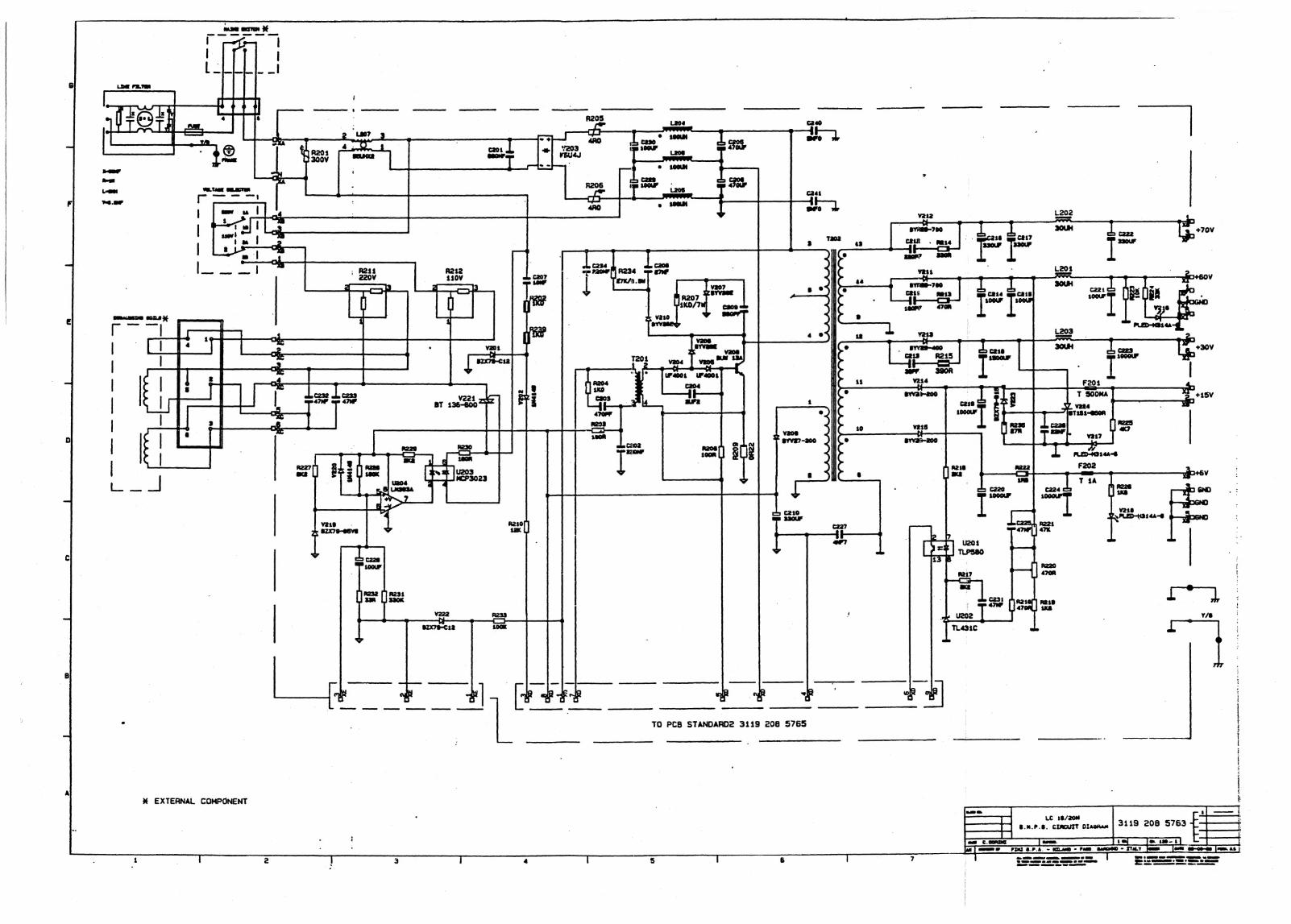
% EXTERNAL COMPONENT
ee CREED AREER Re
TO PCB STANDARDe 3119 208 5765
SN TR LTT EEE
ee ee as
a
eee eee LOT ret t
3 é ¥
H &, E
LC 36/20"
S.m.P.8. CIACUTT OlagAan
A OMS <a mes ee ES
€0 & it) et) 1oF (enw
- OCR ee mee ewe emen ove - ; < ee pot: ede eee Sannegee —aeagemmnen
e oo we ~ . 6 o . , | a
Ct2,4. i
’
4