master ee3102 design proposal - samex entaboutme.samexent.com/.../ee3102designproposal.pdf ·...
TRANSCRIPT

EE3102 Design Proposal
AM Radio
Design Team #11
Samuel Annor Erik Newman Eliot Estrine
Brian Teravskis

Table of Contents System Specifications ................................................................................................ 3 System Block Diagram and Description ..................................................................... 3 Breakdown of Group 11 Tasks ................................................................................... 4 RF-Mixer Subsystem .................................................................................................. 6
Subsystem Specification ...................................................................................... 6 Subsystem Description ........................................................................................ 6 Simulations .......................................................................................................... 8 Prototype Test Results ....................................................................................... 12 Bill of Materials ................................................................................................... 13
RF-IF Amplification and Demodulation Subsystem .................................................. 14 Subsystem Simulations ...................................................................................... 16
AF Subsystem .......................................................................................................... 18 Subsystem Specification .................................................................................... 18 Subsystem Description ...................................................................................... 18 Subsystem Simulations ...................................................................................... 21 Subsystem Bill of Materials ................................................................................ 22
Power Supply Subsystem ......................................................................................... 22 Subsystem Specifications .................................................................................. 22 Subsystem Description ...................................................................................... 23 Subsystem Bill of Materials ................................................................................ 24
Summary/Conclusions .............................................................................................. 24 Unresolved Problems ......................................................................................... 24 Possible Solutions to Problems ......................................................................... 25 Work remaining schedule .................................................................................. 26

System Specifications • Single frequency reception of 1.4 MHz • 1/8 Watt audio output to an 8-ohm load with 5 microvolt RF signal input at 50%
amplitude modulation (provides 115 dB of gain) • Low cost (less than $60.) • Minimal tuning • Selective in the reception of only 1 AM BCB station (10 KHz channel width)
System Block Diagram and Description
Antenna
Speaker
Volume Control
AF Amplifier
RF-IF Amplifier
AM Detector-
Demodulator
IF Filter455 KHz
LocalOscillator
1.855 MHz
MixerRF Filter1.4 MHz
RF-Mixer Subsystem
RF-IF Subsystem AF Subsystem
V
V3
V2
V1
Transformer
Rectifier
Filter
RegulatorSwitch
Power Supply Subsystem
120 VAC
Subsystem Voltages
Power Indicator
Figure 1: AM Radio Block Diagram
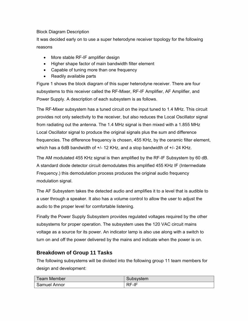
Block Diagram Description
It was decided early on to use a super heterodyne receiver topology for the following
reasons
• More stable RF-IF amplifier design • Higher shape factor of main bandwidth filter element • Capable of tuning more than one frequency • Readily available parts
Figure 1 shows the block diagram of this super heterodyne receiver. There are four
subsystems to this receiver called the RF-Mixer, RF-IF Amplifier, AF Amplifier, and
Power Supply. A description of each subsystem is as follows.
The RF-Mixer subsystem has a tuned circuit on the input tuned to 1.4 MHz. This circuit
provides not only selectivity to the receiver, but also reduces the Local Oscillator signal
from radiating out the antenna. The 1.4 MHz signal is then mixed with a 1.855 MHz
Local Oscillator signal to produce the original signals plus the sum and difference
frequencies. The difference frequency is chosen, 455 KHz, by the ceramic filter element,
which has a 6dB bandwidth of +/- 12 KHz, and a stop bandwidth of +/- 24 KHz.
The AM modulated 455 KHz signal is then amplified by the RF-IF Subsystem by 60 dB.
A standard diode detector circuit demodulates this amplified 455 KHz IF (Intermediate
Frequency.) this demodulation process produces the original audio frequency
modulation signal.
The AF Subsystem takes the detected audio and amplifies it to a level that is audible to
a user through a speaker. It also has a volume control to allow the user to adjust the
audio to the proper level for comfortable listening.
Finally the Power Supply Subsystem provides regulated voltages required by the other
subsystems for proper operation. The subsystem uses the 120 VAC circuit mains
voltage as a source for its power. An indicator lamp is also use along with a switch to
turn on and off the power delivered by the mains and indicate when the power is on.
Breakdown of Group 11 Tasks The following subsystems will be divided into the following group 11 team members for
design and development:
Team Member Subsystem Samuel Annor RF-IF

Erik Newman Power Supply Eliot Estrine AF Brian Teravskis RF-Mixer

RF-Mixer Subsystem
Subsystem Specification • Provide at least 13 dB of conversion gain of the input RF signal • Provide 20 KHz of signal selectivity • Minimize radiated LO signal • LO tunes to 1.855 MHz • IF frequency of 455 KHz • Optional – provide tuning of a segment of the AM broadcast band
Subsystem Description To meet these specifications, and to minimize the cost and development time it was
decided to use the SA612 Integrated Circuit by Philips Semiconductor. This IC uses a
Gilbert-Cell Doubly Balanced Mixer, which provides a conversion gain of 14 dB at 100
MHz, and increases as the frequency decreases. The SA612 also has an internally pre-
biased transistor that can be used as a Local Oscillator.
Figure 2 shows the proposed circuit using the SA612 Gilbert Cell Mixer Integrated Circuit
in the RF-Mixer Subsystem. The Gilbert cell is a cross-coupled differential amplifier
where the gain is controlled by varying the emitter bias current. If a modulating signal is
applied to the emitter bias control the result is a highly linear control of the amplitude of
the RF input voltage. The Gilbert cell configuration used in the SA612 provides a Double
Balanced Modulator. This kind of modulator suppresses the original frequency
components of the mixing process so that only the sum and difference frequency is
present on the output. The suppressions reduces the harmonic content of the output and
eases t he design of any post mixing filtering.
The oscillator section of the SA612 is nothing more than a pre-biased transistor
providing base and emitter connectivity to the external circuitry. It is important to note
that the external circuitry must not alter the bias to this transistor, and often capacitors
are required to isolate the internal DC bias from the external circuitry. There are several
oscillator topologies that can be used with this internal transistor; in this design a Colpitts
Oscillator circuit is employed due to both the stability of the circuit as well as the limited
availability of tapped inductors. An external oscillator may be used with the SA612, but a
limit of 200-300 millivolts must be maintained to prevent overdriving the part.
The SA612 is a good mixer, but has its limitations. The ability of the mixer to handle a
wide dynamic range of RF inputs signals are limited, and therefore usually not desirable
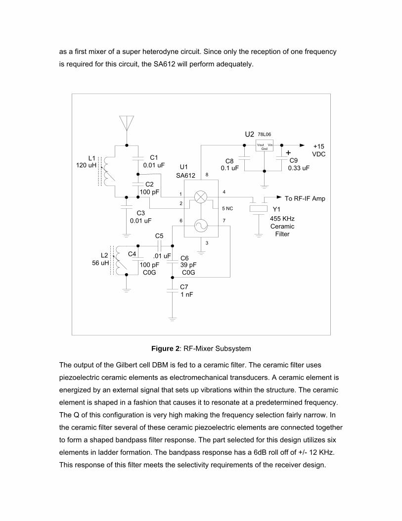
as a first mixer of a super heterodyne circuit. Since only the reception of one frequency
is required for this circuit, the SA612 will perform adequately.
56 uH 100 pFC0G
.01 uF39 pFC0G
1 nF
120 uH
C2100 pF
78L06
VinVoutGnd
0.1 uF 0.33 uFSA612
To RF-IF Amp
+15 VDC
455 KHzCeramic
Filter
U1
C4
C5
C6
C7
C8
Y1
L1
L2
C9C10.01 uF
+
U2
C30.01 uF
1
2
6 7
4
8
3
5 NC
Figure 2: RF-Mixer Subsystem
The output of the Gilbert cell DBM is fed to a ceramic filter. The ceramic filter uses
piezoelectric ceramic elements as electromechanical transducers. A ceramic element is
energized by an external signal that sets up vibrations within the structure. The ceramic
element is shaped in a fashion that causes it to resonate at a predetermined frequency.
The Q of this configuration is very high making the frequency selection fairly narrow. In
the ceramic filter several of these ceramic piezoelectric elements are connected together
to form a shaped bandpass filter response. The part selected for this design utilizes six
elements in ladder formation. The bandpass response has a 6dB roll off of +/- 12 KHz.
This response of this filter meets the selectivity requirements of the receiver design.

Simulations
Front End Tuned Circuit
The SA612 has pre-biased circuitry that must be isolated from external references. The
data sheet recommended a front-end tuned circuit that was adopted for this design and
referenced in Figure 3. This tuned circuit has a center frequency of 1.4 MHz, and has
approximately –30 dB attenuation at 455 KHz and –13 dB attenuation at 1.855 MHz.
This attenuation should minimize the LO and IF frequencies, as well as any other higher
harmonics, from radiating out of the antenna. The antenna has high impedance at 1.4
MHz, and therefore will not load down the tuned circuit when connected directly. Figure
4 shows the LTSpice schematic and simulation of this tuned circuit.
L1120e-6
C1
0.01µ
V1
AC 1Rser=10000
C2
100pC3
0.01µ
.ac dec 40 10000 10000000
Schematic
10KHz 100KHz 1MHz 10MHz-88dB-80dB-72dB-64dB-56dB-48dB-40dB-32dB-24dB-16dB
-8dB0dB8dB
16dB
-160° -140° -120° -100°
-80° -60° -40° -20°
0° 20° 40° 60° 80°
100° V(n002)-V(n003)

Frequency Response
Figure 4: Front-end Tuned Circuit Simulation
Gilbert Cell Mixer
No Spice model of the SA612A could be found, and therefore the equivalent circuit was
used to estimate the amount of conversion gain the mixer would produce at 455 KHz.
The SA612A product specification sheet has an equivalent circuit in figure 4, but there
are internal bias voltages and certain resistors values that are not shown. A best guess
was made using voltage sources, and a current source for the current mirror
(represented by a resistor in the equivalent circuit.) A VHF BJT transistor was used
(2N5089) in the simulation as the SA612A operates up to 500 MHz input frequency.
Figure 3 shows the circuit used in the LTSpice simulator.
The results of the simulation are shown in the FFT of the output waveform at the
collector of Q3. The output frequency is marked and measured at –88.5 dB. With an
input voltage of 5 microvolts, or -106 dB, the conversion gain is 17.5 dB.
Q12N5089
Q22N5089
Q32N5089
Q42N5089
Q52N5089
Q62N5089
R11500
R21500
I1
2e-3
R31500
R41500
Rser=0V1
6
RFSINE(0 5e-6 1.400e6)
V3
.5
V4
.5
R51000
R61000
Rser=500
LO
SINE(0 .2 1.855e6)
R71000
R81000
Vcc
Vcc
Bia
s1
Bia
s1
Bia
s1
Bia
s2
Bia
s2
Bia
s2
.tran 0 100us 0 1e-7
Figure 3: Gilbert Cell Mixer Simulation Schematic
There are many assumptions in this simulation that impact the accuracy as the bias
voltages and current greatly impact the conversion gain, and it is not know what the

manufacturer of the part uses. It is safe to say that a conversion gain of 14 dB or better
(specified in the data sheet) can be realized in the circuit, and therefore meets the
design requirements of the subsystem.
100KHz 1MHz 10MHz160dB 150dB 140dB 130dB 120dB 110dB 100dB -90dB -80dB -70dB -60dB -50dB -40dB V(n001)
455 KHz -88.5 dB
Figure 4: Gilbert Cell Mixer Output FFT
Colpitts Oscillator
As in the Gilbert cell simulation above, the SA612A does not give all of the details
concerning the oscillator BJT parameters. Again, the SA612A oscillator section is
capable of sustaining oscillations up to 200 MHZ, and therefore the simulation uses the
same BJT as was used in the Gilbert cell simulation (2N5089.) Figure 5 shows the circuit
utilized in the simulation, and eventually in the design.

Q12N5089
R118k
R225k
V1
6
L156µH
C1
100p
C2
39pF
C3
.001µF
C4
.01µF
VCC
VCC
.tran 0 100e-3 99.050e-03 10ns
.ic I(L1)=1e-6
Figure 5: Colpitts Oscillator Simulation Schematic
Figures 6 shows the startup, sustained, and FFT transient simulation of the oscillator
used for this design.
0µs 2µs 4µs 6µs 8µs 10µs 12µs 14µs5.44V
5.52V
5.60V
5.68V
5.76V
5.84V
5.92V
6.00V
6.08V
6.16V
6.24V
6.32VV(n002)
Oscillator Startup

44.5µs 45.5µs 46.5µs 47.5µs 48.5µs 49.5µs5.52V
5.60V
5.68V
5.76V
5.84V
5.92V
6.00V
6.08V
6.16V
6.24V
6.32VV(n002)
Oscillator Sustained
100KHz 1MHz-130dB-120dB-110dB-100dB
-90dB-80dB-70dB-60dB-50dB-40dB-30dB-20dB-10dB
V(n001)
Oscillator Spectral Plot
Figure 6: Colpitts Oscillator Simulation Results
Prototype Test Results There were only two of the four tests that were done before this document. Table 1 lists
the test that were required, what was expected as a result, and the measured value.
Measurement Expected Value Measured Result

Mixer conversion gain 14 dB @ 455 KHz 5dB @ 455 KHz
Mixer oscillator frequency 1.855 MHz 1.470 to 1.987 MHz
Mixer oscillator amplitude 200 mVp-p 220 mVp-p
IF selectivity – 3dB roll off 20 KHz 13 KHz
LO front end leakage -30 dB from LO level Not measured
Table 1: RF-Mixer Specification Measurements
The mixer was probably driven into gain compression to make the conversion gain
measurement, as a fairly high voltage input was required to get a reading on the output.
Once the RF-IF amplifier gain is determined the conversion gain will be measured again
at the output of the RF-IF amplifier.
The oscillator coil adjustment will span the AM broadcast band from 1.125 MHz to 1.542
MHz. Just before completing the measurements it was tuned to 1.4 MHz for a final test
in the lab at a later date.
The LO leakage requires a spectrum analyzer connected to the antenna. The plan is to
use the spectrum analyzer in the lab to perform the measurement, but there was not
enough time to complete this before this document was due. It will also be measured at
a later date.
Bill of Materials
Part Number Supplier Qty Each Total RefDes Description
81-CFWLA455KCFA-B0 Mouser 1 $3.35 $3.35 CF1 Filter, Ceramic, 455 KHz
TK2418-ND Digi-Key 1 $4.20 $4.20 L1 COIL 120UH TYPE 7P
TK2414-ND Digi-Key 1 $4.31 $4.31 L2 COIL 56UH TYPE 7PH
568-2089-5-ND Digi-Key 1 $1.75 $1.75 U1 IC MIXER/OSC DOUBLE-BAL 8-DIP
497-1010-ND Digi-Key 1 $0.72 $0.72 U2 78L06 IC POSITIVE REGULATOR 6V TO-92
P4849-ND Digi-Key 2 $0.11 $0.22 C2, C4 CAP 100PF 200V 5% CER RADIAL C0G
495-1007-1-ND Digi-Key 1 $0.16 $0.16 C6 CAP 39PF 100V 5% CER MONO C0G
P4951-ND Digi-Key 3 $0.13 $0.39 C1, C3, C5 .010UF 50V 10% MONOLIT CERM CAP X7R
P4923-ND Digi-Key 1 $0.12 $0.12 C8 .1UF 50V 10% MONOLIT CERM CAP X7R
P4937-ND Digi-Key 1 $0.12 $0.12 C7 CAP 1000PF 50V CERAMIC MONO 5% C0G
P928-ND Digi-Key 1 $0.18 $0.18 C9 KG RAD ALUM ELEC CAP 0.33MFD 50V
RF-Mixer Subsection Total $15.52

RF-IF Amplification and Demodulation Subsystem
Figure 7a: Voltage Feedback Amplifier Configuration in a non-inverting Close-Loop
configuration.
Even though the current feedback amplifier is easier to design than the voltage feedback
amplifier since all it takes is for it to have correct feedback impedance is selected, the
voltage feedback amplifier is used here.
The voltage feedback amplifier is the most abundant amplifier on the market due to their
used in several high speed as well as precision applications. Since the preferred frame
of reference for most analog designers is the voltage feedback amplifier, the stability
analysis begins with the topology shown in Figure 7a. This simplified block diagram
illustrates many of the key characteristics needed in a frequency analysis of the voltage
feedback amplifier. Starting with the input segment of the amplifier, the inputs to the
voltage feedback amplifier are evenly matched. In most cases, the input bias currents
are very close to being the same magnitude and the difference between the two input
bias currents is usually small. Additionally, the input impedances of the amplifier are

close to equal and relatively high. A small error voltage at the input of the amplifier is
gained by the open-loop gain, AOL(s), which is usually fairly high.
The open-loop gain is frequency dependent and starts rolling off at a relatively low
frequency. The resulting open-loop voltage output is the product of the open-loop gain
times the input voltage error.
As expected, the calculation in Figure 1b proves that the closed-loop DC gain is equal to
1 + RF/RIN. At low frequencies the open-loop gain of the amplifier is sufficiently high to
allow for ignoring the gain error. As frequency increases, AOL(s) begins to decrease and
finally becomes the dominant controlling factor in the gain of the circuit. The calculation
of the intersection of the open-loop gain, AOL(s) and the noise gain (also called 1/),
GN = (1 + ZF/ZIN), gives a close approximation to the bandwidth of the closed-loop
amplifier circuit. Gain peaking, which is caused by the phase response of the amplifier
and the feedback circuit, can increase the bandwidth of the closed-loop system at the
expense of decreased stability. The criterion for stability is determined where the closed-
loop noise gain intersects the open-loop gain of the amplifier. Generally, if the phase
margin, at that frequency, is smaller than a theoretical 45 degrees, the circuit can
oscillate given part-to-part variation. A conservative phase margin is more like 60
degrees for flat frequency response.
Fig 7b: Transfer function of the voltage feedback amplifier in a non-inverting
configuration.

The open-loop gain plot of the amplifier assumes a single pole system. As the closed-
loop gain increases, the closed-loop bandwidth decreases.
Matched inputs may or may not be a benefit when using voltage feedback amplifiers. In
addition, offset voltages and offset currents are relatively low compared to the current
feedback amplifier topology. A possible disadvantage of the voltage feedback amplifier is
the very close relationship between the bandwidth and closed-loop gain however in the
AM radio RF amplification such disadvantages are minimized.
V5
15Vdc
0
R1
33k
V
V2
15Vdc
V4
15Vdc
R2
1k
0
0
R7
1k
V
0
U2
AD826/AD+in
-in
V+
V-
Vout2
1
9950
46
R6
33k
0
V1
15Vdc
U3
AD826/AD+in
-in
V+
V-
Vout2
1
9950
46
V325e-6Vac0Vdc
Fig 2a The 2 cascaded inverting voltage amplifier.
Apart from choosing the voltage amplifier for this application, the type of operational
amplifier (Op-Amp) that was chosen Analog Devices’ AD826 op-amp because it has the
GBWP or the Unity Gain Bandwidth of 50MHz.
This will give a close-loop gain close of about 30dB (thus choosing R1=33k and R2=1k
and since dBkk
RR
Av 37.3033133
2
1 =−=−=−= ) from each stage with a carrier
frequency of 455 kHz. From the Bode plot below one can see that the gain is very close
to constant gain and with about a gain of 60db
Subsystem Simulations

Fig 2b The Frequency Response of the output of the cascaded amplifier.
The next was to design the detector circuit which is shown in figure 3a.
R5
10k
R3
1kC2
10n
R4
10M
0
C1
10n
0
V0
0
0
Vmod
FREQ = 1kVAMPL = 0.5VOFF = 0.024
V60Vac15Vdc
Vcar
FREQ = 455kVAMPL = 0.024VOFF = 0
0
D2
D1N5711
Fig 3a Detector circuit.
The detector consists of a Schottky diode with a RC network in front of it. However we
could have had a precise rectifier circuits like the one that is based on the AD8037
which is a clamping operational amplifier. This circuit does not use any diodes to provide
rectification. Problem is it is expensive ($8.00), requires a two rail power supply, and
surface mount is the only thing available at Digi-Key. Very undesirable..
So due to the above reason, the Schottky diode is only 41 cents or so and will do a great
job since with a pull up resistor, of 10MΩ, and a DC supply, of 15V, will ensure that the
1N5711 is always turn on.
From fig 3a, a simple modulator circuit is used to generate the AM consisting of a
Multiplier and the modulating signal and the carrier signal as done in PSpice. A
sinusoidal source at a frequency of 455 kHz is used to represent the carrier signal and a

second source at a frequency of 1 kHz is used to represent the modulating signal. Notice
that the peak amplitude for the carrier is set to 24mvolt, the estimated amplitude of
output signal of the RF amplifier. A typical broadcast
AM signal includes the carrier as well as the sidebands in the transmission. To get such
a double sideband transmitted carrier signal (DSB-TC) we must bias or offset the
modulating signal by a value equal to the carrier's peak voltage.
Fig 3b, Generated AM signal
AF Subsystem
Subsystem Specification • Audible at 6 feet
Subsystem Description The audio amplification subsystem produces the audio output of the entire system. The
input signal is in the range of several millivolts, this value is far to low to drive a speaker
and produce an audible output, and must be amplified. For the output of the radio to be
audible, approximately 1/8th of a watt must be delivered to the speaker. To accomplish
this, the overall gain of the audio amplifier subsystem must be around 45 to 60 dB. In
addition, the circuit must be able to provide significant amount of current to the load
without altering its performance. Finally, this subsystem will be responsible for the
volume control requirements of the radio.

U4
LM386
INN0
INP1
BYP
2G
13
G8
4
OUT 5
VS6
GN
D7
R18
V115Vdc
U5
LM741
+3
-2
V+7
V-4
OUT 6
OS1 1
OS25
V2.0015Vac0Vdc V3
15Vdc
R2
330k
R3
10k
R4150
C1
100uF
C2.047uF
Audio OutputInput fromdecoder stage
Speaker
VV
I
V
Figure 1: The two stage circuit used to produce the audio output. The gain of the circuit
shown is 330.
The output load of this subsystem is an 8 ohm speaker. In addition for the output to be
audible, approximately 1/8th of a watt must be delivered to the speaker. For an 8 ohm
speaker, the current required is:
I = sqrt(P/R) = sqrt((1/8 watts) / (8 ohms)) = 125 mA
A LM741 can provide a maximum of 40 mA and therefore is inadequate for this
application. The output stage also uses an RC network to create a band pass filter and
filter out any signals outside the normal audible range which may have been caused by
noise or resonance effects. The upper cutoff frequency was chosen to be 30 kHz while
the lower cutoff frequency was chosen to be 200 Hz. The speaker itself has a frequency
range of 450 Hz to 13 kHz, so it will provide additional band pass characteristics to the
subsystem.
The primary device used in this subsystem is the LM386 audio power amplifier. This
device has several advantages over the standard operational amplifiers used in lab and
elsewhere in this project. The first, and primary reason for choosing this amplifier, is that
it is able to produce a large output current. In addition, this device only requires a single
power supply. The model chosen was the LM386N-3 because its voltage requirement
closely matched those of other components used in the project. The LM386 uses
internal feedback resistors to produce a gain of 20 without any external resistors.
However, the gain can be varied up to 200 by using external components. Downsides of
this device include lower maximum gain, and a lower gain bandwidth product than other
amplifiers. However, because this stage is only required to amplify audio frequencies,
the lower gain bandwidth did not affect the design.
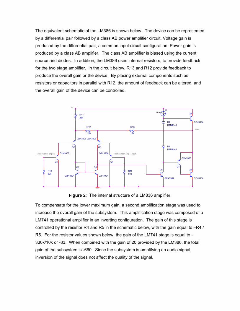
The equivalent schematic of the LM386 is shown below. The device can be represented
by a differential pair followed by a class AB power amplifier circuit. Voltage gain is
produced by the differential pair, a common input circuit configuration. Power gain is
produced by a class AB amplifier. The class AB amplifier is biased using the current
source and diodes. In addition, the LM386 uses internal resistors, to provide feedback
for the two stage amplifier. In the circuit below, R13 and R12 provide feedback to
produce the overall gain or the device. By placing external components such as
resistors or capacitors in parallel with R12, the amount of feedback can be altered, and
the overall gain of the device can be controlled.
Vout
D2D1N4148
Q4
Q2N3906
Q1
Q2N3906
R13
15k
R1430k
Q9
Q2N3904
Q3
Q2N3906
I11mAdc
Q8
Q2N3904
Inverting Input
Q5
Q2N3904
Q6
Q2N3904
D1D1N4148
Q2
Q2N3906
Vs
R12
1.5k
R1550k
Q11
Q2N3906
Q10
Q2N3904
R1150k
NonInverting Input
Figure 2: The internal structure of a LM836 amplifier.
To compensate for the lower maximum gain, a second amplification stage was used to
increase the overall gain of the subsystem. This amplification stage was composed of a
LM741 operational amplifier in an inverting configuration. The gain of this stage is
controlled by the resistor R4 and R5 in the schematic below, with the gain equal to –R4 /
R5. For the resistor values shown below, the gain of the LM741 stage is equal to -
330k/10k or -33. When combined with the gain of 20 provided by the LM386, the total
gain of the subsystem is -660. Since the subsystem is amplifying an audio signal,
inversion of the signal does not affect the quality of the signal.

A potentiometer is used between the LM741 and the LM386 to provide volume control.
By varying the potentiometer, a user can control the voltage division that occurs between
the two stages. If no voltage division occurs, the output will be at maximum value,
however, if the potentiometer is altered, the output volume can be linearly reduced to
nothing.
The functionality of the subsystem was tested using PSpice. The circuit shown above
was simulated, and produced the output shown below. The high pass cutoff frequency
was found to be 197 Hz, while the low pass cutoff frequency was found to be 29.85 kHz.
These numbers are consistent with what was predicted for the circuit. By limiting the
bandwidth of the device, high and low frequency noise can be filtered out to produce a
clearer sound.
Subsystem Simulations
To simulate the LM386 audio amplifier, a new PSpice device and model had to be
created. The model is based on a Spice model created by Dave Dilatush, and made
publicly available.
Figure 3: PSpice simulation of the Audio Amplifier subsystem

The mid-band gain of the subsystem was 678, or 56.4dB. The maximum voltage output
was 1.018 volts for a 1.5mV input. This value was very close to the predicted mid-band
gain of 660. This gain is necessary to produce the 1/8th of a watt power output needed
for the output to be audible. The simulation also showed that the subsystem drew 64mA
of current from the positive voltage supply. This value is within the limits of the power
supply. These results show that the audio amplifier subsystem is predicted to meet the
design requirements.
Prototype test results were very promising. The LM386 operated as expected, and the
gain was found to be almost exactly 20 when no external components were used, and
increasable to 200 is a 10 uF capacitor was placed across the gain pins, shorting the
feedback resistor. However, the LM386 drew more current than expected, especially
when configured for a larger gain. To counteract this, it was decided to use a LM741
gain stage and allow the LM386 to operate at its minimum gain level. This combination
was effective because the total gain of the subsystem could be varied as easily as
adjusting the gain of an inverting amplifier. In addition, this two amplifier configuration
reduced the current draw of the subsystem while maintaining the required gain.
Subsystem Bill of Materials
Part Number Supplier Quantity Cost Total Cost RefDes Description
LM386N-4-ND 1 0.94 0.94 LM741CNNS-ND 1 0.84 0.84 604-1055-ND 2 0.39 0.78 Storeroom 1 0.1 0.1 Storeroom 3 0.09 0.27 102-1186-ND 1 3.5 3.5 Storeroom 1 0.9 0.9 Audio Amp Sub Section Total 7.33
Power Supply Subsystem
Subsystem Specifications
• Power available is standard 110V rms 60Hz
• Power on indicator light

• Power On/Off switch
• Power drawn from source can not exceed 10 watts
• Voltage needed is +15V and -15V
Subsystem Description
The power supply is the most flexible of the subsystems. Due to the power supplies
flexibility and the other subsystems limited options, the power supply was designed to
meet the requirements of the other subsystems.
The power supply uses a peak rectifier circuit with a smoothing capacitor. The peak
rectifier consists of a diode bridge which operates as follows: During the positive half-
cycles vs will be positive and travel through the load. During the negative half-cycles –vs
will be positive and travel through the load. When both the positive and negative half-
cycles travel through the load in the same direction it allows for Vout to be always
positive. The RF-IF Amplifier required the +/- 15 volts so we designed the transformer
bridge rectifier circuit to output two positive 20 Vac lines. Then after regulation we invert
one of the lines to get the desired negative 15 volts.
The voltage regulator was chosen for its output voltage and its current capability. The
amount of current needed was used mostly by the speaker which is about 250mA.
Choosing the MC78M15AC gave a 500mA positive voltage regulation with a 15 volt
output voltage.
One limitation of using the diode bridge is a voltage drop of 1 volt per leg due to the
current passing through two diodes for each half cycle. Also the voltage regulator
needed Vout to be 2 volts higher than Vin. Thus we needed a transformer outputting
greater than 18 volts.
A filter capacitor is used for smoothing the output of the rectifier voltage. In order to pick
an appropriate capacitor value four things are needed: Vp (peak voltage), Vr (ripple
voltage), f (frequency, and R (resistance). The needed capacitor is picked using this
equation:
C=Vp/(Vr*f*R). The audio amp uses approximately 250mA of current which gives a
resistance of about 60 ohms. With the other subsystems taking very little current and all
of the subsystems being in parallel we use the 60 ohms for the resistance value.

V1
110Vac, 60Hz
0C10.1u
U2
MC78M15C/TO
IN1
OUT2
U2
MC78M15C/TO
IN1 OUT 2
C20.1u
- +
U3
MB2S
2
3
4
1
- +
MB2S
2
3
4
1
T3
TRANSFORMER CT
0
-15Volts
+15Volts
0
0
C3u
C4u
0
0
Subsystem Bill of Materials
Part Number Supplier Qty Cost Total Cost RefDes Description
595-1139-ND Digikey 1 10.69 10.69 XFRMR PWR 115V 40VCT 500MA
Digikey 2 Capacitor IC-LM7815T Storeroom 2 0.39 0.78 500mA 15V Regulator CT-35-.1 Storeroom 2 .21 .42 C1,C2 Resin Dipped 0.1uF 35V
Summary/Conclusions The circuit appears to function as it stands, and also receives KLBB as designed. There
are a few issues that need to be addressed in the following sections to refine the design,
and improve the quality of the received signals.
Unresolved Problems 1. Audio amplifier tends to become unstable when the potentiometer is above ½ its
range.
2. The audio amplifier tends to distort the signal badly at larger input levels
3. Possible thermal issues with the LM386 amplifier
4. There is a lot of noise on the signal coming from the RF-IF amplifier
5. The AM detector distorts the signal at low levels
6. The RF-Mixer input tuned circuit is not peaking as it should

7. When factoring in all of the external parts and hardware we are getting close to
the $60 limit
Possible Solutions to Problems 1. This is possibly caused by limitations on the input voltage for the LM386 audio
amplifier. In order to prevent this, the gain provided by the LM386 and LM741
amplifier stages will have to be altered so as to reduce the input to the LM386
while maintaining the same overall subsystem gain. It may also be possible to
add a limiter circuit (consisting of four resistors and two diodes) to reduce the
gain of the LM741 stage when a stronger signal is applied.
2. For the audio amplifier subsystem, future work will focus on improving the quality
of sound produced by the speaker. When driven using a sinusoidal input test
signal, the audio amplifier distorts the top half of the sine wave. This is possibly
because the LM741 stage shares its positive voltage supply with LM386, while its
negative supply voltage is much less loaded. If this is the cause, then the
amplifier stages will need to be better isolated from the power supply.
3. In addition, the power consumption of the subsystem will be addressed. The
LM386 currently produces noticeable heat, even when drawing less than 100mA.
Over short periods of time, this does not present a problem. However, if
operating for an extended period of time in an enclosed container, the amount of
heat produced by the LM386 may become significant. One methods of
addressing this is to add a heat sink to the LM386. Since this component is
responsible for the vast majority of the current draw of the entire system, it is the
only device that heats up significantly. However, a heat sink would have to fit
within the physical constraints of the system. The audio amplifier subsystem
uses several large components such as capacitors, a potentiometer, and a
speaker which take up significant space surrounding the LM386. In addition, a
small amount of air circulation would have to be added, possibly with several
small holes or a vent.
4. The specification for the AD826 RF-IF amplifier is very specific about the layout
of the PC board around the part. It stressed the importance of keeping the inputs
and outputs as separated as possible, and keeping the feedback resistors close
to the device. While the prototype board kept feedback resistors close to the pins

of the part, the small IC mounting boards were just cut from a small PC board
with a Dremel tool. These cuts resulted in the two amplifier sections having their
pins close together, and this might be the reason for the noise observed. The
specification also stressed having both electrolytic and ceramic capacitors
directly connected to the power supplies to keep the voltage stable for low and
high frequency noise. Further power supply decoupling measure might be
required.
5. It appears that the diode is being pulled to some rail limit, and higher input
signals pull it away from that limit. Either the resistor across the capacitor is
responsible for this pulling, or the RF-IF amplifier offset voltage is pulling the
voltage level from ground. More simulation is required to understand the problem
fully. One possible solution is to use a capacitor to block the DC offset voltage on
the RF-IF amplifier from affecting this circuit. As stated earlier, higher input
signals reduce this problem, and the KLBB signal in the lab appeared high
enough to work for this application, and therefore the problem might be
overstated for this design.
6. A lower impedance of the mixer input might swamp the input tuned circuit, and
therefore lowering the Q of the circuit. The specification sheet states that the
input resistance is 1.5 K-ohms. The coil is supposed to have a Q of 80, and that
would result in a resistance (XL/R) of 1.055 K-ohms. The 1.5 K-ohms would be in
parallel with this value and so would broaden the bandpass to an effective Q of
1.7, or a bandwidth of 820 KHz. See next numbered item for possible solution.
7. Some components could be cut to reduce cost. In particular the tuned input
circuit could be removed, as it is not working correctly. This would cut $5.00 from
the circuit cost. Some of the components were priced from the Digi-Key catalog
at the low quantity values (higher dollar amount,) and the stockroom’s prices are
lower as they probably purchase in higher quantities or have an arrangement
with Digi-key for a lower price break. Redoing the pricing of all of the items may
also reduce the cost
Work remaining schedule Table 2 shows the remaining schedule to complete the project.
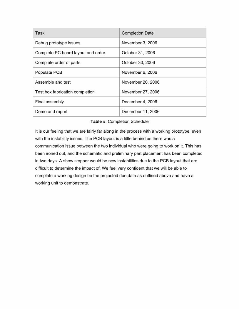
Task Completion Date
Debug prototype issues November 3, 2006
Complete PC board layout and order October 31, 2006
Complete order of parts October 30, 2006
Populate PCB November 6, 2006
Assemble and test November 20, 2006
Test box fabrication completion November 27, 2006
Final assembly December 4, 2006
Demo and report December 11, 2006
Table #: Completion Schedule
It is our feeling that we are fairly far along in the process with a working prototype, even
with the instability issues. The PCB layout is a little behind as there was a
communication issue between the two individual who were going to work on it. This has
been ironed out, and the schematic and preliminary part placement has been completed
in two days. A show stopper would be new instabilities due to the PCB layout that are
difficult to determine the impact of. We feel very confident that we will be able to
complete a working design be the projected due date as outlined above and have a
working unit to demonstrate.