master_thesis_staggered pattern.pdf
TRANSCRIPT

A METHODOLOGY FOR DESIGNING STAGGERED PATTERN
CHARGE COLLECTORS
A Thesis
Presented to
The Academic Faculty
by
Blake Ryan Marshall
In Partial Fulfillment
of the Requirements for the Degree
Master of Science in the
School of Electrical and Computer Engineering
Georgia Institute of Technology
May 2012

A METHODOLOGY FOR DESIGNING STAGGERED PATTERN
CHARGE COLLECTORS
Approved by:
Professor Greg Durgin, Advisor
School of Electrical and Computer Engineering
Georgia Institute of Technology
Professor Andrew Peterson
School of Electrical and Computer Engineering
Georgia Institute of Technology
Professor Paul Steffes
School of Electrical and Computer Engineering
Georgia Institute of Technology
Date Approved: February 10, 2012

To my parents, Joe and Maria, and my brother, Austin

iv
ACKNOWLEDGEMENTS
I wish to thank my family for all their support throughout my education,
specifically, my parents, Joe and Maria, and my brother, Austin. I would also like to
thank Dr. Edward Wheeler for inspiring me to attend graduate school and study
electromagnetics. A special thanks to my committee, Dr. Andrew Peterson and Dr. Paul
Steffes, for dedicating their time and resources to reading my thesis. Finally, I would like
to thank my advisor, Dr. Greg Durgin as well as the students in the Propagation Group
for all of their assistance throughout writing this thesis.

v
TABLE OF CONTENTS
Page
ACKNOWLEDGEMENTS iv
LIST OF TABLES vii
LIST OF FIGURES viii
SUMMARY x
CHAPTERS
I Introduction 1
1.1 Introduction to RFID 1
1.2 Basic Operation of RFID Systems 3
1.3 Introduction to Staggered Pattern Charge Pumps 6
II Staggered Pattern Charge Collector Theory 12
2.1 Basic Patch Antenna Theory 12
2.2 Staggered Pattern Array Beam Steering 16
2.3 Staggered Pattern Beam Optimization 20
2.4 Dickson Charge Pump 25
III Staggered Pattern Charge Collector Design Example 29
3.1 Patch Antenna Design 30
3.2 Staggered Pattern Design Example 33
3.3 Charge Pump Design Example 38
IV Staggered Pattern Charge Collector Example Simulation 40
4.1 Patch Antenna Simulation – CST/HFSS 40
4.2 Staggered Pattern Array Simulation - ADS 49
4.3 Charge Pump Simulation - LTSpice 52

vi
V Conclusion 58
APPENDIX A: Staggered Pattern Array Factor Variation Plots 61
APPENDIX B: Staggered Pattern – Single Array – Simulated Radiation Pattern with
Phase Shift Varied 65
APPENDIX C: Matlab Code for Finding Half-Power Beamwidth and IPCG 69
REFERENCES 78

vii
LIST OF TABLES
Page
Table 1: Integrated Power Conversion Gain Comparison 22
Table 2: Optimization Table for Staggered Pattern Charge Collecting Arrays 23
Table 3: Patch Design Example Properties 33
Table 4: Trace Impedance and Width for Design Example 34
Table 5: Comparison of IPCG of Antenna Simulations 42

viii
LIST OF FIGURES
Page
Figure 1: Basic Energy Harvesting Block Diagram 2
Figure 2: Basic RFID System Diagram 4
Figure 3: Staggered Pattern Array Basic Outline 9
Figure 4: Schematic of One Side of the Staggered Pattern Charge Collector 10
Figure 5: Example Staggered Pattern Array Factor Radiation Pattern 11
Figure 6: Rectangular Patch Layout 13
Figure 7: Basic rectangular Patch Radiation Pattern 15
Figure 8: Matching Techniques for Microstrip Patch Antennas 16
Figure 9: Beam Steering of Two-Element Linear Array 18
Figure 10: Staggered Pattern Array with Patch Antennas – 170 Degree Phase Shift 24
Figure 11: Dickson Charge Pump Schematic (4 Stage Example) 26
Figure 12: Lumped Element Circuit Model of Staggered Pattern Array and
Charge Pump 27
Figure 13: Four Layer PCB Diagram 29
Figure 14: Patch Antenna Design Example Layout 31
Figure 15: Patch Antenna Design Example Layout with Inset 32
Figure 16: Staggered Pattern Design Example Model 33
Figure 17: Staggered Pattern Radiation Pattern for Phase Difference of 160 Degrees
Between Sub-Arrays 36
Figure 18: Design Example of Staggered Pattern Layout 37
Figure 19: Designed 10 Stage Dickson Charge Pump 39
Figure 20: Patch Antenna Simulation Geometry 43
Figure 21: S11 Resonance for Single Patch Antenna 44

ix
Figure 22: 3-Dimensional Radiation Pattern of a Single Patch 45
Figure 23: 2-D Radiation Pattern of a Single Patch 46
Figure 24: 3-D and 2-D Radiation Pattern of a 2-Element Linear Array of Patches 47
Figure 25: 2-D Radiation Pattern for 2-Element Linear Array of Patches with 120
Degree Phase Difference 48
Figure 26: Staggered pattern Array ADS Schematic 50
Figure 27: S11 for Staggered Pattern Array with 50 Ohm Loads 51
Figure 28: Capacitor Parasitic Model 52
Figure 29: Diode Packaging Model for SOT-203 (2 Diodes per Package) 53
Figure 30: 10 Stage Charge Pump DC Voltage Output without Source Impedance 55
Figure 31: 10 Stage Charge Pump with Matching Circuitry for 50 Ohm Source
Impedance 56
Figure 32: Complete Staggered Pattern Charge Collector Layout 57

x
SUMMARY
With higher frequencies now being used in RFID systems, antennas are becoming
much smaller resulting in more space on tags that can be used for innovative array
designs to harvest more wireless energy. This master’s thesis outlines and details a new
methodology for designing and simulating the staggered pattern charge collector, a
technique to improve harvesting wireless energy. Staggered pattern charge collectors
enable RFID tag’s to produce a higher DC voltage from a charge pump circuit by
creatively using multiple arrays to increase the antenna power conversion gain without
limiting the half power beamwidth. This thesis discusses the basics of patch antennas and
charge pumps as well as an optimization technique for the staggered pattern array by
maximizing integrated power conversion gain (IPCG). An example of a staggered pattern
charge collector is fully specified from design through simulation, in preparation for
fabrication. This methodology allows for the staggered pattern charge collectors to be
designed, simulated, and fabricated quickly and effectively.

1
CHAPTER 1
INTRODUCTION
1.1 Introduction to RFID
Radio Frequency Identification (RFID) has rapidly integrated into our world
spanning a gamut of applications. Security access, shipment tracking, animal chipping
and pharmaceutical sales are all common uses for RFID and the list continues to grow.
Many applications prefer RFID to other solutions such as bar code scanning due to
limited space and directional scanning. With RFID, the tag only needs to be in the
general vicinity of the reader, but a bar code scanner, for example, can only “see” the tag
by directly passing the reader over the tag in line of sight.
For example, take the application of tollbooths for vehicles. Before RFID-enabled
tollbooths, there would be an attendant or a bowl to collect the change from each driver
in order to access the toll road. This system resulted in huge lines of cars waiting to pass
through a manual gate one by one. If one person is not prepared or cannot pay, the entire
line must wait. Now, RFID technology allows vehicles to simply pass through an
archway where there is an RFID reader. This reader identifies your vehicle as it passes
through and adds the charge to a personal account stored in a remote database. Supposing
that another technology had been implemented, such as bar code scanning, each car
would still have to stop, resulting in continued long lines of cars. Each car would have to
be stopped and scanned before it could continue on its journey.
For an RFID system in this application, the RFID tag in the car could be quite
large and contain a battery. In other applications such as tracking runners in a race, large
bulky RFID tags are not feasible. In these situations, it is imperative to have a low profile

2
system without the constraint of having a power source located on the tag. For a low
power tag without batteries, one of the best option for power is RF energy harvesting.
The idea behind energy harvesting is utilizing the transmitted wireless power from the
RFID reader to power the tag itself. The benefits of this technique are obvious as there is
no longer a need to have an on board power supply. This reduces weight, size, cost, and
need to replace the battery itself. On the other hand, the disadvantages include
complexity of design and low received power efficiencies.
The current techniques for an energy harvesting device are based upon an antenna
and some flavor of energy harvesting circuitry as shown in Figure 1. This is very sound
in theory but the resulting DC voltage is often not high enough or does not provide
sufficient power to handle many devices. For example, harvesting energy from a 100kW
radio station at 954 kHz with a 6-stage Dickson charge pump can only produce 520 mV
DC at 15 kilometers away. In half an hour, the circuit is only able to harvest 60.2μJ,
which is only high enough to power very simple, low power devices [1].
Figure 1: Basic Energy Harvesting Block Diagram
To increase the DC voltage available at the RFID tag circuitry and harvest more
overall energy, different techniques can be used in conjunction with the same basic
concepts. Some focus on improving the communication or modulation scheme. For
example, a power optimized waveform (POW) alters the modulation waveform to
produce a higher peak voltage while maintaining the same power level [2]. This has a
minimal effect on performance of the RFID systems but dramatically improves the
energy that can be harvested by increasing the DC output voltage. Other methods try to
RFID
Antenna
Energy Harvesting Circuitry
DC Voltage

3
improve the gain of the antennas by not using simply one array but different types of
arrays. One example of such a technique is pattern strobing, where the antenna, or an
array of antennas, creates a very high gain but narrow beam and shifts it around until the
source of the wireless power is "found". When the wireless power source is "found", the
antenna main beam stays focused on the point to get the highest possible DC voltage out
of the energy harvesting circuitry [2]. This can be compared to the game of hide-and-seek
in the sense that it is easier to find someone hiding in a large, dark room with a spotlight
than it is to find them in the same room barely lit all over. There are many other creative
schemes, not belabored in this introduction, which try to improve wireless energy
harvesting by various means.
In this thesis, a methodology for designing and building a staggered pattern array
is developed. Staggered pattern arrays are a creative implementation of multiple antenna
arrays to increase the power conversion gain without narrowing the main beam by using
two or more offset arrays [2].
1.2 Basic Operation of RFID Systems
A basic RFID system consists of a tag and a reader, where the reader is hard
wired to a computer/chip and power supply. When a tag gets within range of the reader,
the reader sends out wireless signals and the tag returns wireless information containing
its ID. The reader then sends the information to the computer/chip for processing.
Because the reader is hard-wired to a power supply, there are few limits on its processing
capabilities. The basics of an RFID system as explained above are shown in Figure 2.

4
Figure 2: Basic RFID System Diagram
RFID tags can be grouped into two general categories: active and passive. Active
tags are powered by internal means, like a battery, and passive tags harvest RF energy.
Active tags tend to be bulkier and more expensive, due to the power source, than their
passive counterparts, which only require some basic energy harvesting circuitry to power
the system. Passive tags typically cannot provide the same power and range capabilities
as active tags, so their applications tend to be for short range and simple communication.
For example, a passive tag should not be used when any complicated operations on a
microcontroller must be performed on tag since the microcontroller must draw a high
current. A passive tag often only powers a simple microcontroller to flip a switch,
creating an open-circuit or short-circuit to vary the antenna feed reflection coefficient.
The reader can identify the tag’s ID based on the wireless signal reflected from the tag
being a positive or negative reflection [15]. Since the microcontroller only needs to flip a
switch, the microcontroller draws very little power and can run off a low DC voltage. In
addition, since the reader's RF signal is modulated and backscattered, the tag does not
need to provide the antenna with its own RF signal to relay the information back to the
reader. This application is ideal for an energy harvesting circuit. Active tags are not
discussed in this thesis because they do not require energy harvesting circuitry, but it is
important to understand which kind is better suited for a certain application.
RFID Reader
Data Processor
RFID Tag
Energy
Harvesting
Circuit
Microcontroller

5
As discussed earlier, passive tags have three main sections: an antenna, an energy
harvesting circuit, and a microcontroller. In the energy harvesting circuitry, a charge
pump converts an AC signal to a DC voltage that powers the microcontroller. There are
many charge pump topologies such as the Buck converter or the Cockcroft-Walton
Voltage Multiplier [4]. These all have their benefits and tradeoffs, but for this application
the Dickson charge pump topology is used. The topology is comprised of several stages
of shunt capacitors connected with series diodes. Each stage has a capacitor that holds
charge. As more capacitor and diode stages are added, the DC voltage on the output
increases, theoretically [4].
The antenna is equally as important when harvesting wireless energy. It is
responsible for receiving the wireless information and power and converting it to a wired
propagation signal. For most RFID tags, the patch antenna or another printed antenna is
used for its low-profile design as well as having about 7 dB gain and a fairly large half
power beamwidth at approximately 60 degrees. Its 7 dB gain over a large beamwidth
makes it a strong choice for energy harvesting since it not highly directional but has a
gain five times that of an isotropic antenna [5].
Finally, the microcontroller is a crucial part of the RFID tag and sets the required
DC voltage and power. For this methodology of designing staggered pattern charge
collectors, it is not important to specify a particular microcontroller, but having an
estimate of the required DC voltage and power is necessary. Most microcontrollers used
in low power RFID applications will have DC operating voltages around 1 to 3.5 V and
the current draw ranges from 0.5 μA to 100 μA during peak power operation [16].
Although the staggered pattern charge pump will increase the amount of energy
harvested, picking a low-power microcontroller is still a primary design consideration for
a passive tag.

6
1.3 Introduction to Staggered Pattern Charge Pumps
Passive tags are preferred over active tags for their small form factor and low
cost, but they are limited by their power consumption. So the question becomes: how can
designs improve the efficiency of the charge pumps and harvest more of the RF energy.
The staggered pattern charge pump is one possible technique to improve wireless energy
harvesting by increasing power conversion gain without lowering the beamwidth.
When RFID began, low frequencies were predominantly used for their low
propagation loss, and batteries were used to power the tags. When the battery-less tag
was introduced, inductive coupling was the most efficient way to transmit power
wirelessly but required very close proximity [6]. Since then, the frequency has continued
to increase, making antennas and feed traces much smaller, in turn, creating more space
for antenna and array designs. In addition to creating more space, higher frequency
systems can also give a boost to the received power. The power conversion gain is
defined as the gain of the antennas as used in the link budget equation in (1). Upon first
glance at a basic link budget, it appears that increased frequency decreases the received
power due to the shrinking wavelength term in the denominator of (1). In actuality, the
antenna power conversion gains cancel out the loss and make power received
proportional to the square of frequency as shown by substituting (2) into the two power
conversion gain terms in (1).
𝑃𝑅𝑋 = 𝑃𝑇𝑋 + 𝐺𝑇𝑋 + 𝐺𝑅𝑋 − 20 log10 4𝜋𝑅
𝜆 (1)
𝐺𝑑𝑖𝑟 𝑎𝑛𝑡 ∝1
𝜆2 (2)
where:
PRX = Power Received (dBm)
PTX = Power Transmitted (dBm)

7
GTX = Gain of Transmitter Antenna (dB)
GRX = Gain of Receiver Antenna (dB)
R = Distance Between Antennas (m)
λ = Wavelength (m)
If two directional antennas are used, the received power actually increases with
frequency. This realization makes using antennas nearly as efficient as inductive coupling
for power and it also, obviously, adds range to your device. So, increasing the frequency
actually increases the power received by the antenna according to the equations below.
Higher received power correlates to a higher AC voltage entering the charge pump,
which in turn creates a higher DC voltage at the output of the charge pump. The higher
DC charge pump voltage allows for a higher power microcontroller to be used which is
capable of more complex operations.
In addition to improved power transfer, the increase in frequency has made the
antennas smaller. This has created space for more creative ways to implement antenna
arrays such as the staggered pattern shown topologically in Figure 3 and as a schematic in
Figure 4. The staggered pattern charge pump uses two arrays of patch antennas and two
charge pumps which terminate on a common capacitor. The final stage of charge pump A
and charge pump B is a single shared capacitor which is connected in parallel with the
load. The term “staggered” is used to show that each antenna array main beam is offset
on either side from the normal direction. An equal but opposite phase difference between
the feeds to each antenna array creates an angle offset in the antenna pattern to each side
from the normal direction. Obviously, according to array theory, a single array’s pattern
is narrowed and the gain is increased [5]. A high gain helps improve the DC voltage
output, but only if the beam is aimed at the reader. Otherwise, very little power is
transferred and the tag cannot operate. By adding a second array and pushing the main
beam of each array to either side of the normal direction, effectively, the two beams with
a higher gain form a larger half power beamwidth as shown in Figure 5. The blue dashed

8
pattern comes from the top array (Patch1 and Patch 2) and the red solid pattern comes
from the bottom array (Patch 3 and Patch 4).
In summary, the staggered pattern design benefits from an increase in power
conversion gain of the antenna system to feed the charge pump, while negating the
disadvantage of a narrower beamwidth by using a second offset array adjacent to it. The
higher power conversion gain corresponds to a higher AC voltage entering the charge
pump which in turn allows for a higher DC voltage on the output of the charge pump and
much higher conversion efficiency. Although there are major benefits, the staggered
pattern charge pump does leave a larger footprint on the tag than a single small antenna.
The higher power conversion gain of the antenna allows the tag to move farther away and
to use a microcontroller with higher power consumption resulting in a more capable
passive tag.
This thesis outlines a methodology for designing staggered pattern charge pumps
by analyzing antenna design, array design, charge pump operations and non-linear
impedance matching. It discusses theory, design, and, finally, simulation.

9
Figure 3: Staggered Pattern Array Basic Outline

10
Figure 4: Schematic of One Side of the Staggered Pattern Charge Collector
Staggered Pattern Antenna Array
Charge Pump

11
Figure 5: Example Staggered Pattern Array Factor Radiation
Pattern

12
CHAPTER 2
STAGGERED PATTERN CHARGE COLLECTOR THEORY
This section presents some basic theory for single patch antennas and investigates
the theory behind staggered pattern collectors. The staggered pattern array uses four
patch antennas in two arrays to create a unique pattern for energy harvesting. The patch
antenna, staggered pattern array, and the charge pump are all introduced through explicit
equations.
The idea of a staggered pattern charge collector has been documented but the
equations governing the array design are not. This chapter presents these equations and
optimizes the staggered pattern array for integrated power conversion gain which can be
used in every staggered pattern charge collector design.
2.1 Basic Patch Antenna Theory
The patch antenna is a popular choice in most RFID systems today for their low
profile, low cost, and easy manufacturability. For many passive, low profile tags, it is a
necessity for the antenna to be easy to produce and to mount [7]. For example, key card
access using RFID is a popular application where it is imperative that the antenna
maintain the sleek form of the card. If a large, highly directional antenna were used, it
would be very difficult to mount on the card. In addition, the antenna must also have a
strong power conversion gain and a broad half power beamwidth, which are tradeoffs in
conventional antenna design. Patch antennas are an elegant choice, but there are some
limitations to the patch antennas including narrow bandwidth and a high impedance,
which can make design more difficult [7].
13
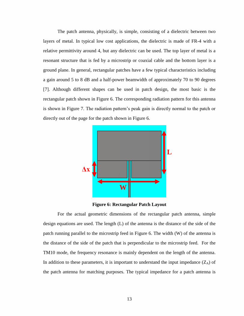
The patch antenna, physically, is simple, consisting of a dielectric between two
layers of metal. In typical low cost applications, the dielectric is made of FR-4 with a
relative permittivity around 4, but any dielectric can be used. The top layer of metal is a
resonant structure that is fed by a microstrip or coaxial cable and the bottom layer is a
ground plane. In general, rectangular patches have a few typical characteristics including
a gain around 5 to 8 dB and a half-power beamwidth of approximately 70 to 90 degrees
[7]. Although different shapes can be used in patch design, the most basic is the
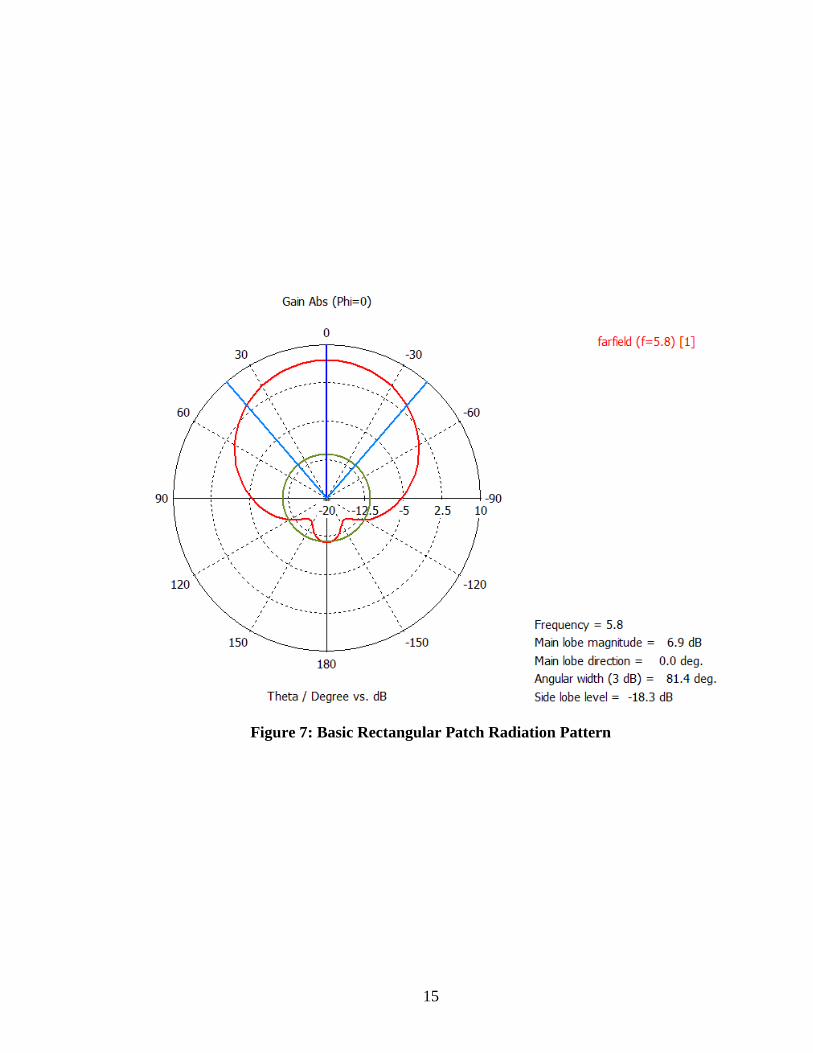
rectangular patch shown in Figure 6. The corresponding radiation pattern for this antenna
is shown in Figure 7. The radiation pattern’s peak gain is directly normal to the patch or
directly out of the page for the patch shown in Figure 6.
Figure 6: Rectangular Patch Layout
For the actual geometric dimensions of the rectangular patch antenna, simple
design equations are used. The length (L) of the antenna is the distance of the side of the
patch running parallel to the microstrip feed in Figure 6. The width (W) of the antenna is
the distance of the side of the patch that is perpendicular to the microstrip feed. For the
TM10 mode, the frequency resonance is mainly dependent on the length of the antenna.
In addition to these parameters, it is important to understand the input impedance (ZA) of
the patch antenna for matching purposes. The typical impedance for a patch antenna is
W
L
Δx

14
between 100 and 300 Ohms while the bandwidth (B) can vary dramatically depending on
relative permittivity (εr), substrate thickness (t), and free space wavelength (λ) [8].
𝐿 = 0.49𝜆
𝜀𝑟 (3)
𝑍𝐴 = 90𝜀𝑟
2
𝜀𝑟−1
𝐿
𝑊
2
(4)
𝐵 = 3.77𝜀𝑟−1
𝜀𝑟2
𝑊
𝐿
𝑡
𝜆 ,
𝑡
𝜆≪ 1 (5)
Equally as important as the antenna design is the feeding structure. The feeding
structure transfers the power from the antenna to circuitry. If the feed does not match the
impedance of the antenna with that of the circuitry, maximum power cannot be
transferred to the circuitry. There are many feeding structures including, but not limited
to, coaxial probe feed, aperture coupled feed, L-band capacitivly-coupled feed, and a
microstrip feed [9]. This thesis only investigates the microstrip feed but the other feed
structures may better fit certain applications for the patch antenna.
The microstrip feed is one of the simplest because it is only a microstrip
transmission line connected to the patch as previously shown in Figure 6. Standard
microstrip transmission line has a 50 Ohm impedance which is unacceptable for a direct
connection to a patch antenna where the impedance is normally between 100 and 300
Ohms [8]. Without a reasonable matching network, the reflection coefficient ranges from
about 30% to 70%, which results in poor power transfer. Two basic techniques for
matching antennas with microstrip feeds are investigated: the quarter-wave transformer
and the inset feed.
The quarter-wave transformer adds an extra quarter wavelength to the feed line
with an intrinsic impedance set to the geometric mean of the real impedances trying to be
matched. For example, a 300 Ohm antenna and a 50 Ohm trace require a 122.5 Ohm
quarter-wave length trace to perfectly match the two lines.
15
Figure 7: Basic Rectangular Patch Radiation Pattern

16
This matching technique when used for matching a feed line to an antenna has no
effect on pattern radiation at all but does take up more space on the PCB. As for the inset
feed, the patch must have an inset cut to allow the trace to run deeper into the patch,
which saves space but may distort the radiation pattern [8].
𝑄𝑢𝑎𝑟𝑡𝑒𝑟 𝑊𝑎𝑣𝑒 𝑇𝑟𝑎𝑛𝑠𝑓𝑜𝑟𝑚𝑒𝑟: 𝑍0′ = 𝑍𝐴𝑍𝑜 (6)
𝐼𝑛𝑠𝑒𝑡 𝐹𝑒𝑒𝑑: 𝑍0′ = 𝑍𝐴𝑐𝑜𝑠
2 𝜋Δ𝑥
𝐿 (7)
Figure 8: Matching Techniques for Microstrip Patch Antennas
Overall, any feed structure and matching network can be used for the staggered
pattern charge collector. The design for a feed structure should be judged depending on
the application and what constraints are presented.
2.2 Staggered Pattern Array Beam Steering
The staggered pattern array, as discussed in the introduction, consists of a pair of
two-element linear arrays with different lengths feeding each antenna. By symmetry of
the staggered pattern charge collector, if the theory of one array is well defined, the
second array is simply the mirror image of the other array; therefore, this section focuses
on only one of the arrays. For a maximum gain in the broadside direction, the two patch
antennas should be separated by a half wavelength as shown in Figure 9 [5].
Quarter Wave Length
Inset Feed
Δx
Zo ZA ZA Zo

17
𝑥1 + 𝑥2 =𝜆
2 (8)
The difference in the lengths creates the phase shift in the feeds (φ) that steers the main
beam of the radiation pattern. To add intuition, assume that a plane wave is incident on
the array from an oblique angle. The closer antenna to the source will receive the wireless
signal first and the farther antenna will receive the wireless signal after a time delay. For
maximum constructive interference, both signals should be completely in phase;
therefore the farther antenna should have a shorter path to the T-connection than the
closer antenna as shown in Figure 9. Note that Figure 9 only shows one array of the
staggered pattern charge collector. Therefore, the radiation pattern steers toward the
antenna with a longer feed as some function of the phase difference between the feeds.
𝑥1 − 𝑥2 = 𝑓 𝜑 (9)
Next, solve for the function dependent on the phase difference, f(φ). First, the time delay
between the feeds is related to the propagation velocity by (10) and (11).
𝑣𝑝 =𝑐
𝜀𝑟 (10)
𝑡1 − 𝑡2 =(𝑥1−𝑥2)
𝑣𝑝 (11)
From this time delay, the phase shift (radians) in the feeds is found simply by multiplying
by the frequency in radians per second. By substitution, (8) and (13) define the lengths.
𝛥𝜑 = 2𝜋𝑓 𝑡1 − 𝑡2 (12)
∆𝜑 =2𝜋𝑓
𝑣𝑝 𝑥1 − 𝑥2 (13)
In summary, since the phase offset in the feeds is now equivalent to some Δx
offset in the length, the standard linear array equation can be used to model the staggered
pattern with the phase shift term [8].

18
Figure 9: Beam Steering of Two-Element Linear Array

19
As previously defined, the staggered pattern uses a pair of two-element arrays
with a phase shift, where the array factor is multiplied with the element factor to create
the radiation pattern. The main lobe is directly normal to the patches when no phase shift
is present. But, if a phase shift is included, each array steers each beam to either side of
the normal direction. The array factor for a single array is given in (14) [5]:
𝐴𝐹 = 𝑎𝑛𝑁𝑛=1 𝑒𝑗 𝑛−1 (𝑘𝑑𝑐𝑜𝑠 𝛾 +𝛽) (14)
where:
an = amplitude factor (constant for symmetrical feeds)
N = number of elements
k = propagation constant (rad/m)
d = array element separation (m)
γ = angle of incidence (rad)
β = feed phase difference (rad)
Recall, there are two arrays, Array A and Array B, each steer their respective
beams to equal but opposite angles from the normal line. So, instead of one array having
a phase difference in the feeds of φ, let charge pump A have a phase difference of
positive φ/2 and charge pump B has a phase difference of –φ/2. By finding the patterns
and overlaying them, the combined pattern can be seen. However, the worst case
condition assumes only one array is on at a time, so the array with the higher power
conversion gain at each angle is assumed to be on. For example, if charge pump A has a
higher power conversion gain, charge pump B is assumed to harvest no energy. In
simulation, this results in taking the maximum of the superposition of the two radiation
patterns. These theoretical plots assist with intuition about how phase difference causes
steering, but to find the actual optimized value for the staggered pattern charge pump, a
numerical simulation involving the antenna factor must be performed. A variation of the
phase difference with the respective array pattern is shown in Appendix A.
20
2.3 Staggered Pattern Beam Optimization
The staggered pattern technique is effective to harvest energy, but the next
question is how to harvest the most RF energy. The optimal angle for steering the beams
is one at which the coverage area and the power conversion gain are maximized. A better
model including some of the antenna pattern characteristics must be developed for
optimization of the staggered pattern array.
An explicit mathematical solution should be used for the patch antenna which
depends on propagation constant (β) and the width of the patch (W) [8]. The
mathematical model of the patch radiation pattern is shown in (15).
𝑓 𝜃 = cos 𝜃sin
𝛽𝑊
2sin 𝜃
𝛽𝑊
2sin 𝜃
(15)
The patch radiation pattern can be referred to as the antenna factor (f(θ)) while the array
factor (AF(θ)) was discussed in 2.2 Staggered Pattern Beam Steering. For an overall
radiation pattern, the square of the product of the array factor and the antenna factor is
used as shown in (16).
𝐺 𝜃 = 𝐹 𝜃 2 = 𝑓 𝜃 𝐴𝐹 𝜃 2 (16)
A benchmark must be developed before any attempt to optimize is possible. As
the phase difference between the antennas is varied, the beamwidth increases but the
beams spread farther apart. For the staggered pattern charge collector, the highest power
conversion gain for the largest amount of possible coverage area is ideal, therefore both
values should be included in the benchmark. The reason for a large beamwidth is because
the source of the wireless power is unknown, and the reason for high power conversion
gain is for a higher AC voltage to the charge pump, which in turn results in a higher DC
voltage output. For an optimization value, the integrated power conversion gain (IPCG) is
computed as the integration of the power conversion gain over the beamwidth. The PCG
is defined in (17) and should be maximized.

21
For the comparison, two different parameters of the antennas including half power
beamwidth and IPCG are shown. The power conversion gain values and beamwidths are
reported with reference to a patch antenna standardized with a unity peak gain. The half
power beamwidth is obtained by finding the two angles that correlate to half power on
the radiation pattern then taking their difference. The IPCG of each is found by
integrating over the beamwidth according to (17), which is used as the optimization
factor.
𝐼𝑃𝐶𝐺 = 𝐺 𝜃 𝑑𝜃𝐵𝑊
(17)
The mathematical simulation results are shown in Table 2 and Figure 10. A phase
difference higher than a 110 degrees and less than 180 degrees resulted in a high
optimization value and approximately 110 degrees resulted in the highest optimization
value. The total radiation pattern when the phase difference is 110 degrees is shown in
Figure 10. It has a beamwidth close to a single patch at 70 degrees but an IPCG of nearly
double that of a single patch. For a two-element antenna array without the staggered
pattern, the integrated power conversion gain is 1.21 with a beamwidth of 50 degrees. If
the single patch, two-element array, and staggered pattern array are all compared by
IPCG, the staggered pattern is vastly superior as shown in Table 1. Although the
beamwidth is reduced by the array, the second array allows for both an increase in power
conversion gain and the superimposed beamwidth. The two-element array keeps IPCG
approximately unchanged as expected from traditional array theory, but by staggering a
second antenna array the IPCG is greatly increased by 38% improvement over the single
patch. Therefore, the staggered pattern array is clearly superior to a single patch antenna
or a two-element array for energy harvesting. In Table 2, the optimization table is shown
to optimize IPCG in terms phase difference between the arrays (φ). Note that there are
abrupt jumps in the IPCG due to the radiation pattern being plotted every 5 degrees, so
the beamwidths are rounded to the nearest factor of ten.

22
Table 1: Integrated Power Conversion Gain Comparison
Single Patch Two-Element Patch
Array Staggered Pattern
Array
Integrated Power Conversion Gain
(IPCG) 1.19 1.21 1.64
By using the optimization information from Table 2 in conjunction with equations
(8) and (13), the lengths of x1 and x2 can be determined. The same values with x1 and x2
switched are used for the second array in the staggered pattern charge pump. For a
particular example of solving for these values, Chapter 3 should be examined.

23
Table 2: Optimization Table for Staggered Pattern Charge Collecting Arrays
Phase Difference (β) (degrees)
Single Patch IPCG SPCC IPCG
IPCG Beamwidth (degrees)
IPCG Beamwidth (degrees)
0 1.19 80 1.21 50
10 1.19 80 1.24 50
20 1.19 80 1.28 50
30 1.19 80 1.31 50
40 1.19 80 1.33 50
50 1.19 80 1.48 60
60 1.19 80 1.50 60
70 1.19 80 1.51 60
80 1.19 80 1.53 60
90 1.19 80 1.53 60
100 1.19 80 1.53 60
110 1.19 80 1.64 70
120 1.19 80 1.63 70
130 1.19 80 1.62 70
140 1.19 80 1.60 70
150 1.19 80 1.58 70
160 1.19 80 1.55 70
170 1.19 80 1.61 80
180 1.19 80 1.58 80

24
Figure 10: Staggered Pattern Array with Patch Antennas – 170 Degree Phase Shift

25
2.4 Dickson Charge Pump
The Dickson charge pump was first described in 1976 by John Dickson as a DC-
DC voltage multiplier [4]. Today, it can be used as an AC-DC charge pump that is
effective as an energy harvesting circuitry. Although the circuit appears simple, there are
many complications that arise due to non-linearities in the diodes, so a designer must
often work with modeling tools to iterate the circuit design numerically. This makes
“matching” an antenna system to a charge pump very difficult. If the charge pump were
linear, a simple complex conjugate match to the charge pump would provide maximum
power transfer. Instead, a more empirical tuning technique is used due to the non-
linearities [4].
In Figure 11, the Dickson charge pump for AC to DC operation is shown. The
charge pump is made up of stages with each containing a diode in series and a shunt
capacitor. Cout and RL will be models of the load for this application, namely, a
microcontroller. The microcontroller input impedance characteristics can be found on the
specification sheet.
During charge pump operation, each capacitor stores charge and pushes the
charge through each of the diodes to the next capacitor to the right. A two case analysis
can be performed to show this conclusion when the input voltage is positive and when the
input voltage is negative. When the input is below zero, C1 and C3 starts charging from
the ground and current is pulled up through the first and third diode. When the input
moves above zero, the charge is pushed from C1 on to C2 and from C3 to Cout. Then, the
cycle repeats again and charge continues to build on Cout until a DC steady state is
reached on Cout. Once steady state is reached, the process continues to a lesser degree
holding a DC voltage on the output with a small ripple [3].

26
AC
RLCoutC1 C2 C3
Figure 11: Dickson Charge Pump Schematic (4 Stage Example)
The equations derived by Dickson use two square waves on the input instead of
an AC source and a ground as shown in Figure 11. The equations are still valid for the
AC-DC case as long as the frequency is low enough that the capacitor can fully charge
after each cycle. This is an assumption that is made to use the following equation for the
output voltage [4]:
𝑉𝑜𝑢𝑡 = 𝑁+1 𝑉𝑖𝑛 −𝑉𝑡
1+𝑁
𝑓𝐶𝑅𝐿
(18)
There are a few results that should be noticed upon looking at this equation. First,
with a high frequency and fairly large RL and CL, as the number of stages (N) increases,
the output voltage continues to increase. Also, with each additional stage, an additional
threshold voltage of the diode (Vt) is subtracted from the input voltage. If too many
stages are connected, the threshold voltage drops will completely kill the input voltage
leaving no voltage on the output. Clearly, the number of stages will have to be designed
based on how large of an input voltage is possible [3].
To find the input voltage to the charge pump for a staggered pattern array, we
plug transmitter gain (GT), receiver power conversion gain (GR), power transmitted (PT),
wavelength (λ), and distance apart (r) into the link budget equation.
𝑃𝑅𝑋 = 𝑃𝑇𝑋 + 𝐺𝑇𝑋 + 𝐺𝑅𝑋 − 20 log10 4𝜋𝑅
𝜆 (1)

27
At this point, assumptions or approximations need to be made about the
application for the system including: the farthest distance the tag will be away from the
reader, the gain of the transmitter, and the power transmitting. The frequency should have
already been chosen from the antenna and the gains can be found during simulation.
After all of these have been determined, the power received is determined, which can be
used to find an equivalent voltage source (Vant) to represent the antenna. (19) shows the
equation for the circuit model below given the power received (PRX) and the impedance
of the antenna (Zant) which we assume to be 50 Ohms.
𝑉𝑎𝑛𝑡 = 2𝑃𝑅𝑋𝑍𝑎𝑛𝑡 (19)
Figure 12: Lumped Element Circuit Model of Staggered Pattern Array and Charge
Pump
With the circuit model in Figure 12, the charge pump gets the maximum voltage
across it when the real part of its impedance is infinite and there is no imaginary part [3].
Since the impedance of the charge pump is unknown and can vary depending on the
voltage or frequency that it sees, a series inductor and shunt capacitor should be added to
the model, so they can be varied to make the best possible match for the non-linear
circuitry. In addition, if the design is at a high frequency such as 5.8GHz, the parasitics of
the packaging for the diodes and capacitors should be added. This model will be further
discussed in the design section of this thesis. The model for the charge pump is now
complete and has been mathematically related to the staggered pattern array.
50 Ohm
Charge
Pump
Impedance Vant

28
Overall, the analysis of a staggered pattern charge pumps may be broken into
three parts: the patch, the array, and the charge pump. The theory behind the staggered
pattern charge collector is well defined and can now be designed and simulated for a
specific application.

29
CHAPTER 3
STAGGERED PATTERN CHARGE COLLECTOR DESIGN
EXAMPLE
This chapter focuses on the design of a staggered pattern charge collector. It
outlines all the steps required to fully design and specify all dimensions and components.
The design is an example so many values that could vary are picked and specified for this
example. The general equations used are from Chapter 2 Theory. The general design for a
staggered pattern charge pump should be performed in the following order:
1. Design Single Patch Antenna
2. Design Staggered Pattern Array
3. Design Dickson Charge Pump
The staggered pattern charge collector designed in this chapter will operate at 5.8GHz
using a 4 layer board with the geometry shown in Figure 13.
Figure 13: Four Layer PCB Diagram
The antennas and traces are placed on the top layer of copper with the 2nd
layer serving as
a ground plane. Another technique is to put the antennas on the bottom layer and use the
third layer as the ground plane. The antennas would radiate from the bottom and the rest
of the circuitry would operate on the top layer. In this case, the antennas would be fed

30
from vias instead of the microstrip as used in this example. The benefit of placing the
antennas on the bottom layer is that the antenna radiation patterns are unaffected by the
circuitry. As for the physical dimensions of the board, the substrate between the first and
second layers has a thickness of 9.3 mil (0.23622 mm) [10]. The relative permittivity is
found to be 3.9 from previously manufactured PCB. The disadvantage is the complexity
of the design since the via may not be exactly 50 Ohms.
3.1 Patch Antenna Design Example
The patch antenna design is very straightforward and the equations from the
theory chapter can be used [8]. However, for this example, a slightly different set
equations that can be used to create an antenna that radiates efficiently and ensures a
fairly small patch width. First, let us define our variables as stated below under the
assumption that W/h > 1 so the subsequent equations are valid [5].
W = width of patch
L = length of patch
ΔL = adjustment length
h = dielectric thickness
fr = resonant frequency
εr = relative permittivity
εeff = effective relative permittivity
For an efficient radiator, (20) defines the width of the patch given the resonant frequency
of 5.8 GHz, relative permittivity of 3.9, and the velocity of propagation as 3(108) meters
per second [5].
𝑊 =𝑣0
2𝑓𝑟
2
𝜀𝑟+1 (20)
Next, let us find the effective relative permittivity, which takes into account that some
fields on the patch antenna are in the dielectric while others are in the air. Given the
board layout, the dielectric thickness is 0.236 mm for an antenna on the top layer [10].

31
The width of the patch was found from (20) and (21) shows that the effective permittivity
is about 2.56 [11].
𝜀𝑒𝑓𝑓 =𝜀𝑟+1
2+
𝜀𝑟−1
2 1 + 12
𝑊 −
1
2 (21)
Now, using the width of the patch, the dielectric thickness, and the effective permittivity,
the length adjustment is found. The ideal length for the resonant patch antenna is a half
wavelength if all the fields were internal to the dielectric, but with some fields outside of
the dielectric, the length must be adjusted. Using (22) and (23), we find the length of the
patch to be 16 mm [5].
𝛥𝐿
= 0.412
𝜀𝑒𝑓𝑓 +0.3 (𝑊
+0.264)
𝜀𝑒𝑓𝑓 +0.258 (𝑊
+0.8)
(22)
𝐿 =𝜆
2− 2𝛥𝐿 (23)
From the design above, we have found the width and length of the patch antenna that will
be used for the staggered pattern array. Figure 14 shows a very basic layout of the patch
where the length (L) is 16 mm and the width (W) is 16.5 mm.
Figure 14: Patch Antenna Design Example Layout
After designing for resonance at 5.8 GHz, the impedance of the patch should be
found so feed and matching structures can be developed. The microstrip feed is being
used in this case with an inset to match the patch antenna to the 50 Ohm transmission
line. Before solving for the inset and trace impedance, let us find the impedance of the
W
L

32
patch. The input impedance of the patch is given by (4) and found to be about 445 Ohms
[8].
𝑍𝐴 = 90𝜀𝑟
2
𝜀𝑟−1
𝐿
𝑊
2
(4)
Clearly, this impedance is much larger than the 50 Ohm microstrip feed and must be
matched properly for full power transfer to and from the patch antenna. Note that the
width (W) could be increased to make the impedance 50 Ohms, but this creates a much
larger footprint for the staggered array.
As earlier stated, this example design will use an inset matching technique but the
quarter wave transformer is just as valid. Recall, the inset technique has the microstrip
feed run deeper into the patch a certain distance (Δx) to match the antenna impedance to
the feed. For this design example, a 50 Ohm feed (Zo’) and a 445 Ohm antenna (ZA) need
to be matched using (7).
𝑍0′ = 𝑍𝐴𝑐𝑜𝑠
2 𝜋Δ𝑥
𝐿 (7)
Now, after solving for Δx, we have found that the trace must enter the patch antenna 6.3
mm to match the antenna with a 50 Ohm trace.
Figure 15: Patch Antenna Design Example Layout with Inset
Table 3 summarizes all the values found for the patch which will be used as the design
example continues to the staggered pattern array portion.
W
L
Δx

33
Table 3: Patch Design Example Properties
Patch Property Value
Resonant Frequency 5.8 GHz
Length 16 mm
Width 16.5 mm
Antenna Impedance 445 Ohms
Inset 6.3 mm
Input Impedance with Inset 50 Ohms
3.2 Staggered Pattern Design Example
For the staggered pattern design portion, let us treat the antennas as 50 Ohm loads
and use the model in Figure 16. The input impedance to the entire staggered pattern
should remain 50 Ohms to ensure maximum power transfer through the entire system.
Figure 16: Staggered Pattern Design Example Model
Notice that ZA and ZB were set to 50 Ohms in the patch design and a T-connection is used
to feed the charge pump. Therefore, Z1 sees ZA in parallel with ZB so Z1 must be 25 Ohms
to keep the entire system matched. The output impedance needs to be 50 Ohms so a
quarter wave transformer should be added after Z1 [12]. If all these techniques are done
correctly, the output impedance should be 50 Ohms. Also, with all the impedances
matched perfectly, the lengths of the traces do not matter except for the lengths that steer
the beam.
50 Ohm Load
50 Ohm Load
Z1
ZA
ZB

34
With the T connection and the quarter wave transformer, the system will require
three unique trace sizes. One, obviously, must be 50 Ohms. The second is used between
the quarter wave transformer and the T connection (Z1) where the impedance is two 50
Ohm loads in parallel resulting in a 25 Ohm impedance. Finally, one trace size must be
used for the quarter wave transformer to transform the 25 Ohm line back to 50 Ohms
which from (6) results in a 35 Ohm trace. A better design that may or may not be possible
would be to use 100 Ohm traces from the patches since the patches have high impedances
and the trace after the T-connection would be 50 Ohms already. This not only decreases
the inset on the patches, but also eliminates the need for the quarter wave transformer at
the output. For a thicker board, this may be possible and optimal, but in this design
example, the 100 Ohm traces are too thin for fabrication.
𝑍 =60
𝜀𝑒𝑓𝑓ln
8
𝑊0+
𝑊0
4 𝑓𝑜𝑟
𝑊0
≤ 1 (24)
𝑍 =120𝜋
𝜀𝑒𝑓𝑓 𝑊0
+ 1.393 + 0.667 ln
𝑊0
+ 1.444 𝑓𝑜𝑟
𝑊0
> 1 (25)
From (24) and (25), the widths for each of the traces can be found and are summarized in
Table 4.
Table 4: Trace Impedance and Width for Design Example
Trace Impedance Trace Width
50 0.57 mm
25 1.57 mm
35 0.99 mm
With the trace widths set and the patch antennas designed, the final step before
the charge pump is to design the lengths that create the staggered pattern (x1 and x2).
Recall from the Theory chapter equations (8) and (13) which were derived from two
conditions:

35
1. The array produces a maximum gain when the antennas are separated by half
a wavelength.
2. A phase difference in the feeds results in a beam that is steered by an angle to
one side of the normal direction.
Also, recall that the optimized phase difference between antennas is between 110 and 180
degrees. Let us design the example for a 160 degree phase difference between the arrays.
𝜋
180(
160
2 𝑑𝑒𝑔𝑟𝑒𝑒𝑠) = ∆𝜑 =
2𝜋𝑓
𝑣𝑝 𝑥1 − 𝑥2 (13)
𝑥1 + 𝑥2 =𝜆
2 (8)
The velocity of propagation (vp) is the speed of light divided by the square root of the
relative permittivity (εr) while the wavelength (λ) in (8) is found for air. Therefore x1 is
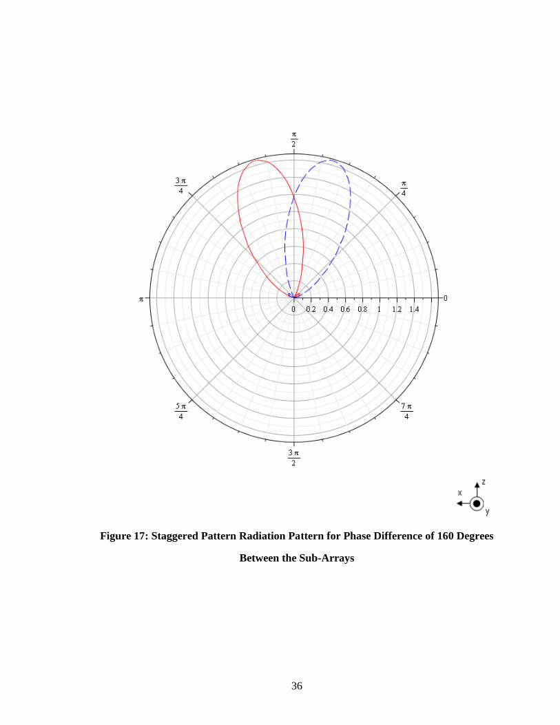
18.8 mm and x2 is 7.1 mm. The expected gain pattern for these lengths is shown in Figure
17. The blue gain pattern is from the top array in Figure 18 and the red gain pattern is
from the bottom array.
In summary, the patch and the staggered pattern array are now fully designed and
only the charge pump remains. In Figure 18, the layout of an entire staggered pattern
array designed for 5.8 GHz, a 50 Ohm load, and a phase difference of 160 degrees
between antennas with all lengths and widths is identified.
36
Figure 17: Staggered Pattern Radiation Pattern for Phase Difference of 160 Degrees
Between the Sub-Arrays

37
Figure 18: Design Example of Staggered Pattern Layout
Charge Pump 1
16.5 mm
18.8 mm 7.1 mm
16 mm
6.3 mm
0.57 mm
Charge Pump 2
1.57 mm
0.99 mm

38
3.3 Charge Pump Design Example
Finally, the Dickson charge pump must be fully defined for the entire staggered
pattern charge pump tag to be complete. For the Dickson charge pump, the number of
stages, capacitor size, and diode must all be defined. The input to the charge pump is the
positive-going wave from the array and the output of the system is a DC voltage (Vout)
which drives a load. The input voltage is defined by the voltage output of the staggered
pattern array and the output voltage is defined by the load that must be driven, such as a
microcontroller.
For this design example, Texas Instruments’ MSP430F2013 microcontroller will
be used as the load. The input resistance is 2 kOhms with a capacitance of 27 pF and a
required DC operating voltage of 2.2 V. The input voltage is defined by (1) with some
assumptions about the power transmitted (Pt), gain of the transmitter antenna (Gt), and
the maximum distance of operation (r). Let us assume to be transmitting 30 dBm of
power from an antenna with a gain of 6 dB at a maximum of 0.5 meter away. Also,
instead of simulating to find the tag's antenna power conversion gain (GRX), the patch
antenna has a gain at about 6 dB and an array of two elements separated by half a
wavelength should give an additional 3 dB. Therefore, the receiver should have a power
conversion gain around 9 dB. Using the link budget shown in (1), the power received
(PRX) is found to be 3.3 dBm.
3.3 𝑑𝐵𝑚 = 30 + 6 + 9 − 20 log10 4𝜋(0.5)
0.052 (1)
Now, if the power is converted to Watts, the received power is 2.15 mW which
can, then, be expressed as a voltage (VA) as given in (26). Therefore, the input voltage
(Vin) is a 500 mV AC signal with a frequency 5.8GHz.
𝑉𝐴 = 2 𝑃𝑅 𝑍 = 2 2.46𝑚 50 = 0.5 𝑉 (19)
The input voltage is 500 mV and the design goal of the charge pump is a 2.2 V DC signal
on the output to power a load. In order to use the output voltage equation to design for the

39
number of stages (N), the diode and capacitors must be chosen. The diode should have a
low turn on threshold (Vt) to ensure the diodes get turned on during each cycle. One
microwave diode has a threshold voltage of 100 mV which is low enough for this
application. The capacitors should be chosen to ensure that they can charge and discharge
quickly, because they need to charge and discharge faster than a single period. The period
of a 5.8 GHz signal is 0.2 ns, so choosing 1 pF capacitors results in a time constant of 50
ps. This gives the capacitors enough time to charge and discharge over one period [4].
Finally, the output voltage equation can be used and shown in (18) to find the
number of stages by taking the largest integer of the number. For the 2.2 V output, the
Dickson charge pump requires 10 stages [13].
𝑉𝑜𝑢𝑡 = 𝑁+1 𝑉𝑖𝑛 −𝑉𝑡
1+𝑁
𝑓𝐶𝑅𝐿
(18)
The final design schematic of the charge pump is shown in Figure 19 and replaces each
of the charge pumps' boxes shown in Figure 18. This completes the design of a staggered
pattern charge pump and the simulation portion begins. Keep in mind during simulation
that these values are all ideal and that many values will need to be adjusted.
Figure 19: Designed 10 Stage Dickson Charge Pump

40
CHAPTER 4
STAGGERED PATTERN CHARGE COLLECTOR EXAMPLE
SIMULATION
The final step before layout and fabrication is simulation. Simulation eliminates
all the assumptions used in the design equations and confirms or adjusts the design so it
works when fabricated. The process of simulation for a staggered pattern charge pump
uses three different types of simulations: antenna simulation, microwave circuit
simulation, and circuit simulation. The antenna simulation is for the patch antenna and
uses ANSYS High Frequency Structure Simulator (HFSS), CST Microwave Studio
(CST), or a similar electromagnetic numerical solver. The microwave simulation includes
the staggered pattern array with all the traces, arrays, and antennas which will be done
with Agilent Advanced Design System (ADS). Finally, the circuit simulation will be
performed in LTSpice. By combining all these simulations, the staggered pattern charge
pump is simulated from wireless input signal to the DC voltage powering the
microcontroller.
4.1 Patch Antenna Simulation – CST/HFSS
The patch antenna designed in the previous chapter is simulated using CST.
Initially, the simulation should use the same parameters as found in the design but may
quickly change if the simulation does not yield the correct results. Upon the first
simulation with the design parameters, the resonance was found near 5 GHz, which
means the antenna needs to be shortened according to (3) because the wavelength
shortens as the resonant frequency increases [5]. The length of the antenna is adjusted to
12.1 mm and the inset can also be recalculated to be 4.3 mm to create the maximum
41
power transfer and minimize S11. S11 should be, at the very least, under -10 dB so 90%
of the power gets through. With the final geometry shown in Figure 20, the S11 is found
to be about -16 dB at 5.8 GHz and the peak power conversion gain is 6.9 dB, which are
shown in Figures 21 and 22, respectively.
The S11 plot shows resonance at 5.8 GHz, but notice how quickly the S11 jumps
back to 0 dB. This means that a small variation in fabrication could result in an antenna
that does not work at 5.8 GHz. One solution is to choose a thicker substrate which would
increase the patch bandwidth; the patch, however, is an inherently narrowband structure.
In this example, the bandwidth of 26 kHz is considered sufficient for this antenna [8].
Also, the half power beamwidth can be found by looking at a constant x plane as shown
in Figure 23. The beamwidth is about 80 degrees as we had optimized it to be in the
theory section.
After the single patch is simulated and operating as expected, the next step is to
find the radiation pattern of a two-element array. Since the optimal distance apart for a
broadside fire array is a half wavelength, two patches with resonance at 5.8 GHz should
be separated by 25.9 mm. This increases the power conversion gain but limits the
beamwidth as shown in Figure 24. The additional power conversion gain is the beneficial
while the loss of beamwidth is counteracted by the second array staggered in the opposite
direction. In Figure 25, the phase difference of 120 degrees is chosen instead of a large
phase difference, because the beams become steered too far apart, resulting in a decrease
in the power conversion gain at θ = 0 degrees. After adjusting the phase difference, the
gap is closed and the beamwidth becomes about 90 degrees with a peak power
conversion gain of 8.1 dB.
In summary, the patch needed some adjustments to center the resonance at 5.8
GHz and the inset had to be adjusted for maximum power transfer. In addition, the phase
difference between the array elements had to be adjusted to 120 degrees to ensure
maximum coverage. Table 5 shows a summary of the patch, basic array, and staggered

42
pattern array based on beamwidth and the integrated power conversion gain (IPCG). The
IPCG is defined in (17) as the integration of gain over the beamwidth. The staggered
pattern array outperforms both the single patch and simple array dramatically in IPCG.
Table 5: Comparison of IPCG of Antenna Simulations
Single Patch Two-Element Array Staggered Pattern
Array
IPCG 2.82 2.80 3.62
Half Power Beamwidth (degrees)
80 50 90

43
Figure 20: Patch Antenna Simulation Geometry
4.3 mm
16.5 mm
12.1 mm
Substrate Thickness: 0.236 mm
PEC Thickness: 0.03429 mm
0.2 mm

44
Figure 21: S11 Resonance for Single Patch Antenna

45
Figure 22: 3-Dimensional Radiation Pattern of a Single Patch

46
Figure 23: 2-D Radiation Pattern of a Single Patch

47
Figure 24: 3-D and 2-D Radiation Pattern of 2-Element Linear Array of Patches

48
Figure 25: 2-D Radiation Pattern for 2-Element Linear Array of Patches with 120
Degrees Phase Difference

49
4.2 Staggered Pattern Array Simulation - ADS
After simulating the resonant patch at 5.8 GHz and simulating the array with
offset, the simulation is transferred from CST to ADS where the staggered pattern layout
is built. Initially, the antennas are replaced with 50 Ohm loads to simplify the simulation.
Since the antennas are designed to have a 50 Ohm impedance with the inset, the load
replacement is a valid substitution.
Next, the microstrip systems are built according to the widths of the traces and the
lengths of the staggered pattern offset portion from Figure 18, but the offset is now 120
degrees. The lengths feeding each of the antennas are now 17.3 mm and 8.6 mm. The
ADS schematic is shown in Figure 26.
After building the schematic, the S-parameters are simulated to investigate S11 as
shown in Figure 27. Upon first simulation, the S11 is, most likely, not minimized at 5.8
GHz. S11 must be at least lower than -20 dB at the output of each trace at 5.8 GHz,
otherwise the width of each trace needs to be adjusted until the condition is met. Once
S11 is minimized at 5.8 GHz, the schematic can be exported to a layout. Figure 27 shows
S11 with 50 Ohm terminations used to model the antenna loads. Since the S11 is near -30
dB at 5.8GHz, the entire system is matched to 50 Ohms. Notice that from 5 to 7 GHz the
impedance stays close to 50 Ohms. This does not remain true when the antennas are
connected because patches are inherently narrowband. The entire staggered pattern layout
is only matched to 50 Ohms at 5.8 GHz when the antennas replace the 50 Ohm loads.
The new values are the corrected design values. Simulation gives much more
accurate values to what they should actually be for the fabricated staggered pattern
charge collector. These are the values that will be used for fabrication.

50
Figure 26: Staggered Pattern Array ADS Schematic
11.3 mm
8.6 mm

51
freq (5.000GHz to 7.000GHz)
S11
5.5 6.0 6.55.0 7.0
-25
-20
-30
-15
Frequency
Ma
g.
[dB
]
S11
Figure 27: S11 for Staggered Pattern Array with 50 Ohm Loads

52
4.3 Charge Pump Simulation - LTSpice
With the entire staggered pattern array simulated successfully, the charge pump
can be simulated and matched to the 50 Ohm source impedance. As found in the design
example, the 10 stage Dickson charge pump with 1 pF capacitors, as shown in Figure 19,
will meet the load specifications of the microcontroller. These load specifications
include: 27 pF capacitance, 2k Ohm input resistance, and 2.2 V DC output. Using this
information, LTSpice can simulate a circuit model of the charge pump.
First, a diode model is uploaded into LTSpice. The Avago HSMS-286x Series is a
strong candidate for its low turn-on voltage around 100 mV [14]. The characteristic
values of the diode can be added to the LTSpice library. In addition to the characteristic
values of the diode, the parasitics of the packaging should be added to the model. Since
the system is operating at 5.8 GHz, it is important to include parasitics for charge pump
circuitry. Using an application note from the Avago specification sheet, the model for the
SOT-23 package can be used for the diode as shown in Figure 29. In addition, shown in
Figure 28, a model for the capacitor packaging should be included by adding a resistance
and inductance in series where the inductance creates a self-resonance at 10 GHz [17].
For the 1 pF capacitors being used in this 10 stage charge pump, the inductor is 253 pH
and the resistor is 30 mOhms.
Figure 28: Capacitor Parasitic Model

53
Figure 29: Diode Packaging Model for SOT-23 (2 Diodes per Package)

54
By using the diodes and capacitors with their respective parasitic packaging
models, a more complicated 10-stage Dickson charge pump circuit can be evaluated. Due
to the large size of the circuit, a schematic is not included but should contain five of the
diode packages (2 diodes per package) and 10 capacitor models with a load of a 27 pF
capacitor in parallel with a 2 kOhm resistor. When simulated with a 500 mV peak-to-
peak voltage at a frequency of 5.8GHz, the steady state DC voltage reaches about 2.3 V
as expected from the design and shown in Figure 30.
After confirming that the circuit performs power harvesting, the next step is to
add the 50 Ohm source impedance and match the charge pump to the 50 Ohm input.
Since the charge pump has a very low impedance, almost no power transfers to the input
of the charge pump. Since the charge pump has a non-linear impedance with input signal
amplitude, traditional matching techniques do not work. However, if the 50 Ohm source
impedance is transformed to a lower value close to 2.5 Ohm, most of the power transfers
to the charge pump load. To transform the impedance, a quarter wavelength stub tuner is
added before the load. The stubs should have an impedance of the square root of 125, or
about 11.2 Ohms. At 11.2 Ohms, the tuner stub needs to be 2.9 mm wide and have a
length of 6.6 mm which can be adjusted after fabrication for optimal matching. Now, the
model is adjusted from having a 50 Ohm source impedance to having a 2.5 Ohm source
impedance which pushes almost all the source voltage to the terminals of the charge
pump. The DC voltage is still not high enough so the capacitors should be increased to 5
pF to get a higher output voltage. After making these adjustments, the new circuit model
and output voltage are shown in Figure 31. The output voltage reaches steady state
around 2.1 V which is enough to turn on the microcontroller.
With this final piece, the entire staggered pattern charge collector is simulated in
multiple portions and is ready for fabrication. Figure 32 shows the final layout out for the
staggered pattern charge collector at 5.8 GHz producing 2.2 V at the load with an
operational range up to 1 m with the given gains and transmit power.

55
Figure 30: 10 Stage Charge Pump DC Voltage Output without Source Impedance
Charge Pump 500 mVpp
5.8 GHz
Load
2k+jω(27p) Vout

56
Figure 31: Charge Pump with Matching Circuitry for 50 Ohm Source Impedance
Vout Load
2k+jω(27p) Charge Pump 500 mVpp
5.8 GHz
50 Ω λ/4
Tuner

57
Figure 32: Complete Staggered Pattern Charge Collector Layout
Charge Pump 1
16.5 mm
17.3 mm 8.6 mm
12.1
mm
4.3 mm
0.37 mm
Charge Pump 2
1.21 mm
0.81 mm

58
CHAPTER 5
CONCLUSION
With increasing popularity in passive RFID devices, energy harvesting has
become increasingly important. The staggered pattern charge collector is one technique
that can convert more wireless energy into useable DC voltage for on-tag devices. This
thesis has developed a complete methodology for designing, optimizing, and simulating
staggered pattern charge pumps.
The staggered pattern charge pump contains three main portions: the antennas, the
staggered pattern array, and the charge pump. For most applications, a patch antenna is
used in the staggered pattern array. The patch antenna is a narrowband antenna with a
low-profile form making it ideal for many passive RFID tag devices. It has a 7 to 8 dB
peak gain and a wide beamwidth around 80 degrees. The design and simulation is
straightforward and has been demonstrated in this thesis using a 5.8 GHz patch antenna
with a peak gain of 6.9 dB and a beamwidth of 81.5 degrees.
For the staggered pattern array, a new optimization parameter was developed,
defined as the integrated power conversion gain over the beamwidth (IPCG). By finding
the highest value of IPCG, a high power conversion gain over a large area can be
achieved. Traditionally, gain and beamwidth are tradeoffs in antenna array design, but
this is not true for the staggered pattern array. Therefore, the optimal phase difference
between the antennas in the array was found to maximize IPCG. With a patch antenna,
the optimal staggered pattern array has a phase difference of 110 to 180 degrees which
will double the power conversion gain while preserving the half power beamwidth that is
normally greatly reduced in an array. With this theory developed, the staggered pattern
can be designed and simulated. In the simulated example, the phase difference between
the arrays was 120 degrees, which resulted in a beamwidth of about 90 degrees and a

59
peak gain of 8 dB. The higher gain is a benefit from the array while using two arrays that
are staggered benefits the beamwidth dramatically. The combination of these two creates
the ultimate combination for harvesting more wireless energy.
Finally, the theory behind designing charge pumps was introduced. For the
example, a microcontroller load was used that required 2.2 V and had 2kΩ input
resistance and 27 pF input capacitance. By using a simple link budget with a few
assumptions, the voltage seen by the charge pump is found to be 500 mV peak-to-peak.
With this information, the number of stages for the charge pump must be ten. The 10-
stage Dickson charge pump is then modeled with all packaging parasitics since operation
is at a high frequency (5.8 GHz) where parasitics have a noticeable effect. In addition, a
matching stub is added to reduce the source impedance so most of the input voltage gets
to the terminals of the charge pump. With a higher voltage at the input terminals of the
charge pump, the DC output voltage is higher. If the input voltage to the charge pump is
under the threshold voltage for the diode, the Dickson charge pump is unable to operate.
After simulation with the source impedance reduced to 2.5 Ohm, the output voltage is 2.1
V DC and can power the microcontroller.
Overall, the staggered pattern charge collector allows for more efficient energy
harvesting by increasing the power conversion gain and the beamwidth of the antennas.
The charge pump design remains the same, but there is one for each antenna array with a
final shared stage to power the load. The final layout for the 5.8 GHz example is shown
in Figure 32 in the Simulation chapter.
As for future research in staggered pattern charge collectors, larger, more
complicated arrays could be used. For example, a four element array creates an even
narrower main beam but has a very high gain. By using four of these arrays, the
beamwidth can be increased and a much higher IPCG is obtained. The tradeoff is that
more space is taken up on the tag. The four four-element staggered pattern array would

60
have four main beams all offset from each other to create a very high power conversion
gain antenna network with a large beamwidth.
Another area for possible work would be to add an array in the 3rd
dimension on
the plane of the PCB. This would narrow the beam in the other direction and another
staggered pattern which could be used. So in reality, it would be two staggered pattern
arrays in two different spatial directions. It would increase the power conversion gain and
the beamwidth in two dimensions instead of just one. The power conversion gain would
go up twice that of the staggered pattern charge collector described throughout this thesis.
In conclusion, this thesis has produced a methodology for designing staggered
pattern charge pumps to more efficiently harvest wireless energy in RFID systems. By
breaking traditional beamwidth and gain tradeoffs with a second array, the staggered
pattern charge collector can receive at a high power conversion gain over a large area to
more efficiently convert wireless signals into DC power.

61
APPENDIX A
STAGGERED PATTERN ARRAY FACTOR VARIATION PLOTS
Appendix A demonstrates how the array factor varies for the staggered pattern
charge collector as the phase difference in gradually increased. The polar plots show the
maximum of the two array patterns on a linear scale. The antenna set up is the same
staggered pattern configuration as used throughout the thesis. The plots have two array
factors and the maximum of the two array factors is taken and plotted in the table below.
PHASE DIFFERENCE
(DEGREES) ARRAY FACTOR PATTERN
0 DEGREES
10 DEGREES
20 DEGREES

62
30 DEGREES
40 DEGREES
50 DEGREES
60 DEGREES
70 DEGREES

63
80 DEGREES
90 DEGREES
Maple code to generate the plots in Appendix A:
64

65
APPENDIX B
STAGGERED PATTERN – SINGLE ARRAY – SIMULATED
RADIATION PATTERN WITH PHASE SHIFT VARIED
The following table demonstrates the phase shift between the two antennas on a single
array. It is plotted on a dB scale and shows the simulated response of a single array on a
staggered pattern charge pump. The plots show the product of the antenna factor and the
array factor in theory and depict the steering of the main beam as the phase shift
increases. The simulation is half the staggered pattern configuration from Figure
PHASE SHIFT
BETWEEN TWO
ANTENNAS
RESULTING RADIATION PATTERN
10 DEGREES
20 DEGREES

66
30 DEGREES
40 DEGREES
50 DEGREES
60 DEGREES

67
70 DEGREES
80 DEGREES
90 DEGREES
100 DEGREES
110 DEGREES

68
120 DEGREES
130 DEGREES
140 DEGREES

69
APPENDIX C
MATLAB CODE FOR FINDING HALF-POWER BEAMWIDTH AND
IPCG
%--------STAGGERED PATTERN THEORETICAL AND SIMULATION CALCULATOR-
---------
%----------------------------------------------------------------
---------
%////////////////////////////////////////////////////////////////
//////////
% This program takes in simulated data and calculates the
Integrated Power
% Conversion Gain (IPCG). This value is the integration of the
Power
% Conversion Gain which is the "gain" used for the link budget
% equation. This program compares the IPCG and beamwidth (BW) for
a single
% patch,two element array, and the staggered pattern array.
%
% In addition, the second part of the program calculates the
expected
% theoretical IPCG from the patch dimensions and varys the phase
% difference in the feeds to create a "steered" beam.
%
% Directions:
% 1. Add imported data to SummaryData.csv in directory.
% 2. Col 1 = Angle, Col 2 = Single Patch Gain, Col 3 = Two
Element Array
% Gain, Col 4 = Staggered Pattern Array Gain
% 3. Run the program.
% 4. Check the finalarray_simulated for results.
% IPCG BW Normalized IPCG
% Single x x x
%Two Element Array x x x
%Staggered Pattern x x x
%
% This program was created by Blake Marshall of the Georgia Tech
Propagation
% Group.
% Advisor: Greg Durgin
% Date: 2/4/2012
%----------------------------------------------------------------
---------

70
clear all;
clc;
%----------------------------------DATA IMPORTER-----------------
---------
%////////////////////////////////////////////////////////////////
/////////
%Imports data
%Col 1 = Angle
%Col 2 = Single Patch
%Col 3 = Two Element Array
%Col 4 = Staggered Pattern Array 2x2
importfile('SummaryData.csv');
angle = (pi/180)*data(:,1);
angle(length(angle)+1)=angle(1); %connecting lines for plot
dangle=angle(2)-angle(1);
single = data(:,2);
single(length(single)+1)=single(1);
array = data(:,3);
array(length(array)+1)=array(1);
stagPatt_half = data(:,4); %60 Degrees per array
stagPatt_half(length(stagPatt_half)+1)=stagPatt_half(1);
%Mirrors Stagg Patt Radiation Pattern to simulate the 2nd array
% May need to change the +1 on the second loop if data is even or
odd.
i=1;
while i < round(length(stagPatt_half)/2);
stagPatt(i,1)=stagPatt_half(length(stagPatt_half)-i);
i=i+1;
end
while(i < length(stagPatt_half)+1);
stagPatt(i,1)=stagPatt_half(i);
i=i+1;
end
%////////////////////////////////////////////////////////////////
/////////
%---------------------------------END DATA IMPORTER--------------
---------
%-------------------------------PLOTTING TO CHECK DATA-----------
--------
%////////////////////////////////////////////////////////////////
//////////
%figure(1)
%polardb(angle,single-max(single));
%figure(2)
%polardb(angle,array-max(array));
%figure(3)

71
%polardb(angle,stagPatt-max(stagPatt));
%////////////////////////////////////////////////////////////////
/////////
%-----------------------END PLOTTING TO CHECK DATA---------------
---------
%-----------------------FIND BEAMWIDTH AND PEAK GAIN-------------
---------
%////////////////////////////////////////////////////////////////
/////////
%Single Patch
ind = find((single - max(single))==0);
singleMaxAngle = angle(ind)*(180/pi);
peakGain_single = single(ind);
three_dB_single = peakGain_single - 3;
sorted_single = sort(single);
j=1;
while j <= length(sorted_single);
if sorted_single(j) > three_dB_single
closest=j;
break;
end
j=j+1;
end
temp = sorted_single(j);
singleBW_ind = find(single==temp);
single_BW = 2*angle(singleBW_ind(1))*(180/pi);
%Array
ind = find((array - max(array))==0);
arrayMaxAngle = angle(ind)*(180/pi);
peakGain_array = array(ind);
three_dB_array = peakGain_array - 3;
sorted_array = sort(array);
j=1;
while j <= length(sorted_array);
if sorted_array(j) > three_dB_array
closest=j;
break;
end
j=j+1;
end
temp = sorted_array(j);
arrayBW_ind = find(array==temp);
array_BW = 2*angle(arrayBW_ind(1))*(180/pi);

72
%Staggered Pattern Array
ind = find((stagPatt - max(stagPatt))==0);
stagPattMaxAngle = angle(ind)*(180/pi);
peakGain_stagPatt = stagPatt(ind);
three_dB_stagPatt = peakGain_stagPatt - 3;
sorted_stagPatt = sort(stagPatt);
j=1;
while j <= length(sorted_stagPatt);
if sorted_stagPatt(j) > three_dB_stagPatt
closest=j;
break;
end
j=j+1;
end
temp = sorted_stagPatt(j);
stagPattBW_ind = find(stagPatt==temp);
stagPatt_BW = 2*angle(stagPattBW_ind(1))*(180/pi);
%////////////////////////////////////////////////////////////////
/////////
%---------------------END FIND BEAMWIDTH AND PEAK GAIN-----------
---------
%------------------------INTEGRATION OVER BEAMWIDTH--------------
---------
%////////////////////////////////////////////////////////////////
/////////
%Single
i=1;
sum=0;
while i < singleBW_ind;
sum = 10.^(single(i)./20)*dangle+ sum;
i=i+1;
end
single_intBW = 2*sum;
%Array
i=1;
sum=0;
while i < arrayBW_ind;
sum = 10.^(array(i)./20)*dangle + sum;
i=i+1;
end
array_intBW = 2*sum;
%Staggered Pattern Array
i=1;
sum=0;
while i < stagPattBW_ind;
sum = 10.^(stagPatt(i)./20)*dangle + sum;

73
i=i+1;
end
stagPatt_intBW = 2*sum;
%Normalized Results
stagPatt_intBW_norm=stagPatt_intBW/(10^(peakGain_stagPatt(1)/20))
;
array_intBW_norm=array_intBW/(10^(peakGain_array(1)/20));
single_intBW_norm=single_intBW/(10^(peakGain_single(1)/20));
%Final results table
finalarray_simulated(2,2)=single_intBW;
finalarray_simulated(3,2)=array_intBW;
finalarray_simulated(4,2)=stagPatt_intBW;
finalarray_simulated(2,3)=single_BW;
finalarray_simulated(3,3)=array_BW;
finalarray_simulated(4,3)=stagPatt_BW;
finalarray_simulated(2,4)=single_intBW_norm;
finalarray_simulated(3,4)=array_intBW_norm;
finalarray_simulated(4,4)=stagPatt_intBW_norm;
%////////////////////////////////////////////////////////////////
/////////
%---------------------END INTEGRATION OVER BEAMWIDTH-------------
---------
%^^^^^^^^^^^^^^^^^^END OF SIMULATION DATA^^^^^^^^^^^^^^^^^^^^^^^
%***************START THEORY SECTION****************************
%----------------------CONSTANTS---------------------------------
----------
%////////////////////////////////////////////////////////////////
/////////
j=sqrt(-1);
f=5.8e9;
er=3.9;
c=3e8;
v=c/sqrt(er);
lamda=v/f;
n=2;
W=18e-3;
k=(2*pi)/lamda;
d=lamda/2;
%////////////////////////////////////////////////////////////////
/////////

74
%-----------------LOOP VARYING PHASE DIFFERENCE BETWEEN ARRAYS---
--------
%////////////////////////////////////////////////////////////////
///////
beta=0; %Phase difference from one array to
%ground (the 2nd array has -beta offset)
dbeta=5; %Steps that beta takes
while beta <=90
%-------------Creates Array Factor and Radation Pattern------
--------
%////////////////////////////////////////////////////////////////
///
po=1;
AF=0;
while po <= n
temp = j.*(po-1).*k.*d.*cos(angle + 90*(pi/180));
temp2=temp+j.*(po-1).*(pi/180).*beta;
AF=AF+exp(temp2);
po=po+1;
end
%Creates Radiation pattern for Patch
fpatt=(cos(angle).*sin(((k.*W)./2).*sin(angle)))./(((k.*W)./2)...
.*sin(angle));
test=1;
nanarray=isnan(fpatt);
while test<length(nanarray)+1
if nanarray(test)==1
fpatt(test)=1;
end
test=test+1;
end
%Calculate Gain pattern with AF*F(theta)
gainpattern=(abs((AF.*fpatt)).^2)/2;
%erases data under ground plane for patch
err=round(length(fpatt)/4);
while err<= round(3*length(fpatt)/4)
fpatt(err,1)=0;
err=err+1;
end
%erases data under ground plane for array factor
err=round(length(gainpattern)/4);
while err<= round(3*length(gainpattern)/4)
gainpattern(err,1)=0;
err=err+1;
end

75
garp=round(3*length(gainpattern)/4)+1;
garp2=round(3*length(gainpattern)/4)+1;
while garp<=length(gainpattern)
gainpattern_plot(garp) = gainpattern(garp2-
round(length(gainpattern)/2));
garp=garp+1;
garp2=garp2-1;
end
garp=1;
while garp<=round(length(gainpattern)/4)
gainpattern_plot(garp) = gainpattern(garp);
garp=garp+1;
end
%figure((beta/dbeta)+1)
%polar(angle, gainpattern_plot(:));
%////////////////////////////////////////////////////////////////
///
%----------------FIND BEAMWIDTHS AND PEAK GAIN---------------
--------
%////////////////////////////////////////////////////////////////
////
%Single Theory Patch Find -3dB
ind = find((fpatt - max(fpatt))==0);
fpattMaxAngle = angle(ind(1))*(180/pi);
peakGain_fpatt = fpatt(ind(1));
three_dB_fpatt = peakGain_fpatt/2;
sorted_fpatt = sort(fpatt);
q=1;
while q <= length(sorted_fpatt);
if sorted_fpatt(q) > three_dB_fpatt
closest=q;
break;
end
q=q+1;
end
temp = sorted_fpatt(q);
fpattBW_ind = find(fpatt==temp);
fpatt_BW = 2*angle(fpattBW_ind(1))*(180/pi);
ind = find((gainpattern - max(gainpattern))==0);
patternMaxAngle = angle(ind)*(180/pi);
peakGain_pattern = gainpattern(ind);
three_dB_pattern = peakGain_pattern/2;

76
% Use the peak gain as a starting location and
%then find the halfpower point going one direction in the
array then
%the other and check to see if it is passed the normal
direction. If
%passed the normal direction just DOUBLE the first angle. If
above the
%normal angle then subtract and double for BW.
% Find
if ind<length(gainpattern)
q=ind+1;
else
q=1;
end
while q>0;
if gainpattern(q) < three_dB_pattern
first=q;
break;
else
if q < length(gainpattern)
q=q+1;
else
q=0;
end
end
if q==ind
throw(err); % ERRROR NO HALF POWER BEAMWIDTH
end
end
if ind>1
q=ind-1;
else
q=length(gainpattern);
end
while q>0;
if gainpattern(q) < three_dB_pattern
second=q;
break;
else
if q > 1
q=q-1;
else
q=length(gainpattern);
end
end
if q==ind
throw(err); % ERRROR NO HALF POWER BEAMWIDTH

77
end
end
temp = gainpattern(q(1));
patternBW_ind = find(gainpattern==temp);
%Finding Beamwidth of Stagg Patt
if angle(second) > 0
pattern_BW = (angle(first)- angle(second)).*2.*(180/pi);
intint=first;
pattern_intGain = 0;
while angle(intint) < angle(second)
pattern_intGain = pattern_intGain +
gainpattern(intint).*dangle.*2;
intint=intint+1;
end
else
pattern_BW = angle(first).*2.*(180/pi);
intint=first;
pattern_intGain = 0;
while angle(intint) > 0
pattern_intGain = pattern_intGain +
gainpattern(intint).*dangle.*2;
intint=intint-1;
end
end
%////////////////////////////////////////////////////////////////
///
%Single Theoretical Patch
%Integrates over the BW
i=1;
sum=0;
while i < fpattBW_ind;
sum = fpatt(i)*dangle + sum;
i=i+1;
end
fpatt_intBW = 2*sum;
%Final Theoretical Table
final_theo((beta/dbeta)+1, 1) = beta;
final_theo((beta/dbeta)+1, 2) = fpatt_intBW;
final_theo((beta/dbeta)+1,3) = fpatt_BW;
final_theo((beta/dbeta)+1, 4) = pattern_intGain;
final_theo((beta/dbeta)+1,5) = pattern_BW;
%Increase beta for the next table part
beta=beta+dbeta;
end

78
REFERENCES
[1] MASAKI, M. and KOIZUMI, H. “An Experimental Result Using RF Energy
Harvesting Circuit with Dickson Charge Pump,” IEEE International Conference on
Sustainable Energy Technologies, 2010, 4 pages.
[2] DURGIN, G., KOO, G., and LU, Y. “Wireless Without Batteries: Extraordinarily
Low-Powered Microwave Communications,”
http://www.propagation.gatech.edu/Archive/PG_CP_110310_GDD/PG_CP_110310
_GDD.pdf. Technical Report, Propagation Group Georgia Tech, 2010.
[3] TROTTER, M. and DURGIN, G. “Effect of DC to DC Converters on Organic Solar
Cell Arrays for Powering DC Loads,” M.S. Georgia Tech, 2008, 87 page,
http://www.propagation.gatech.edu/Archive/PG_TR_081210_MST/PG_TR_081210
_MST.pdf.
[4] DICKSON, J. F., “On-Chip High Voltage Generation in MNOS Integrated Circuits
Using an Improved Voltage Multiplier Technique,” IEEE Journal of Solid-State
Circuits, Vol SC-11, No. 3, 1976.
[5] BALANIS, C. A., Antenna Theory: Analysis and Design. New York: John Wiley &
Sons, 1997.
[6] SCHOLZ, P, et al., “Analysis of Energy Transmission for Inductively Coupled RFID
Tags,” IEEE International Conference on RFID, Las Vegas, April 2007.
[7] LIN, P, et al., “Design of Patch Antenna for RFID Reader Applications,”
Identification in Communication International Conference, 2009.
[8] STUTZMAN, W. L. and THEILE, G. A., Antenna Theory and Design. New York:
John Wiley & Sons, 1998.
[9] RATHOD, J. M., “Comparative Study of Microstrip Patch Antenna for Wireless
Communication Application,” International Journal for Invention, Vol. 1, No. 2,
June 2010.
[10] Advanced Circuits PrePreg Thickness Chart.
http://www.4pcb.com/media/PrePreg%20Thickness%20chart.pdf

79
[11] BEVELACQUA, P.J., “Microstrip (Patch) Antennas,” http://www.antenna-
theory.com/antennas/patches/antenna.php#fringing. 2008.
[12] POZAR, D. M., Microwave Engineering. New York: John Wiley & Sons, 2004.
[13] ZHANG, M. and LASER, N., “Optimization Design of the Dickson Charge Pump
Circuit with Resistive Load,” Circuits and Systems IEEE, Vol 5, September 2004.
[14] Avago Specification Sheet - HSMS-286x Series
[15] DOBKIN, D. M., The RF in RFID. New York: Elsevier Inc, 2008.
[16] Texas Instruments Microcontroller Specification Sheets – MSP430F2013,
MSP430F2619, MSP430L092, MSP430F5619
[17] American Technical Ceramics – 600S Series Microwave Capacitors
http://atceramics.com/product_specifications.aspx?id=30#ContentPlaceHolder2_Re
peater4_Image1_3